EP3557645B1 - Film packaging structure and display apparatus having same - Google Patents
Film packaging structure and display apparatus having same Download PDFInfo
- Publication number
- EP3557645B1 EP3557645B1 EP18849544.4A EP18849544A EP3557645B1 EP 3557645 B1 EP3557645 B1 EP 3557645B1 EP 18849544 A EP18849544 A EP 18849544A EP 3557645 B1 EP3557645 B1 EP 3557645B1
- Authority
- EP
- European Patent Office
- Prior art keywords
- layer
- inorganic film
- sub
- film layer
- thin
- Prior art date
- Legal status (The legal status is an assumption and is not a legal conclusion. Google has not performed a legal analysis and makes no representation as to the accuracy of the status listed.)
- Active
Links
Images
Classifications
-
- H—ELECTRICITY
- H10—SEMICONDUCTOR DEVICES; ELECTRIC SOLID-STATE DEVICES NOT OTHERWISE PROVIDED FOR
- H10K—ORGANIC ELECTRIC SOLID-STATE DEVICES
- H10K59/00—Integrated devices, or assemblies of multiple devices, comprising at least one organic light-emitting element covered by group H10K50/00
- H10K59/80—Constructional details
- H10K59/87—Passivation; Containers; Encapsulations
- H10K59/873—Encapsulations
- H10K59/8731—Encapsulations multilayered coatings having a repetitive structure, e.g. having multiple organic-inorganic bilayers
-
- H—ELECTRICITY
- H01—ELECTRIC ELEMENTS
- H01L—SEMICONDUCTOR DEVICES NOT COVERED BY CLASS H10
- H01L23/00—Details of semiconductor or other solid state devices
- H01L23/28—Encapsulations, e.g. encapsulating layers, coatings, e.g. for protection
- H01L23/31—Encapsulations, e.g. encapsulating layers, coatings, e.g. for protection characterised by the arrangement or shape
-
- H—ELECTRICITY
- H10—SEMICONDUCTOR DEVICES; ELECTRIC SOLID-STATE DEVICES NOT OTHERWISE PROVIDED FOR
- H10K—ORGANIC ELECTRIC SOLID-STATE DEVICES
- H10K50/00—Organic light-emitting devices
- H10K50/80—Constructional details
- H10K50/84—Passivation; Containers; Encapsulations
- H10K50/844—Encapsulations
- H10K50/8445—Encapsulations multilayered coatings having a repetitive structure, e.g. having multiple organic-inorganic bilayers
-
- H—ELECTRICITY
- H10—SEMICONDUCTOR DEVICES; ELECTRIC SOLID-STATE DEVICES NOT OTHERWISE PROVIDED FOR
- H10K—ORGANIC ELECTRIC SOLID-STATE DEVICES
- H10K71/00—Manufacture or treatment specially adapted for the organic devices covered by this subclass
-
- H—ELECTRICITY
- H10—SEMICONDUCTOR DEVICES; ELECTRIC SOLID-STATE DEVICES NOT OTHERWISE PROVIDED FOR
- H10K—ORGANIC ELECTRIC SOLID-STATE DEVICES
- H10K2101/00—Properties of the organic materials covered by group H10K85/00
- H10K2101/80—Composition varying spatially, e.g. having a spatial gradient
Definitions
- the disclosure relates to the field of display technology, and more particularly, to a thin-film encapsulation structure, a manufacturing method, and a display apparatus therewith.
- the encapsulation technology is a common technology for organic light-emitting diode (OLED).
- OLED organic light-emitting diode
- the object of encapsulating an organic light-emitting diode is to protect the organic light-emitting diode, and more particularly, to prevent a light-emitting layer of the organic light-emitting diode from damages caused by moisture or oxygen.
- OLED is encapsulated by way of encapsulation with glass powders, encapsulation with a cover attached with drying sheets or the like to improve the moisture and oxygen barrier capabilities.
- these encapsulation structures can only be used in rigid displays but not in flexible displays, resulting in limiting the development of flexible display technologies
- US 2015/288811 A1 discloses a flexible organic light emitting display (OLED) device including an organic emitting diode arranged on a flexible substrate, and an encapsulation film covering the organic emitting diode and including a first inorganic layer and an organic layer.
- the first inorganic layer is made of a first material, and at least a portion of the first inorganic layer includes a dopant that increases the surface energy of the doped material compared to that of non-doped material.
- US 2012/912451 A1 discloses a thin film encapsulation method, which applies a PECVD method, deposition thin film on the device surface to separate the devices' active area from the water vapor and oxygen in the air, so as to realize the physical protection and thus to accomplish the device encapsulation, specifically, comprising the following procedures: (1) placing the devices to be encapsulated in the PECVD chamber, and fixing the mask to control the encapsulation area; and (2) depositing the inorganic layer, the polymer layer and the graded composition layer by using the organic silica precursor through the PECVD method under the plasma condition and obtain the required encapsulation structure.
- CN 106 298 848 A discloses an organic light emitting diode display including: a substrate; an organic light emitting diode on the substrate; a capping layer on the organic light emitting diode and including a high refractive layer including an inorganic material having a refractive index that is equal to or greater than about 1.7 and equal to or less than about 6.0; and a thin film encapsulation layer covering the capping layer and the organic light emitting diode.
- US 2017/125732 A1 and US 2011/097533 A1 also disclose thin film encapsulation stacks for OLED devices wherein one inorganic layer in the stack has a graded refractive index.
- the present application provides a thin-film encapsulation structure for improving moisture and oxygen barrier capabilities. Furthermore, the present application further provides a method for manufacturing the same, and a display apparatus with such thin-film encapsulation structure.
- the thin-film encapsulation structure includes a plurality of inorganic film layers and at least one organic film layer which are laminated alternately at one side of an organic light-emitting diode.
- the plurality of inorganic film layers includes N inorganic film layers including a first inorganic film layer to an N-th inorganic film layer arranged sequentially from inside to outside, N ⁇ 2.
- each inorganic film layer has a refractive index increasing gradually from inside to outside.
- the first inorganic film layer includes M sub-layers including a first sub-layer to an M-th sub-layer arranged sequentially from inside to outside, M ⁇ 2.
- the M sub-layers of the first inorganic film layer have refractive indexes increasing sub-layer by sub-layer from the first sub-layer to the M-th sub-layer.
- the M sub-layers of the first inorganic film layer have thicknesses increasing sub-layer by sub-layer from the first sub-layer to the M-th sub-layer.
- Each of the plurality of inorganic film layers has a refractive index increasing gradually from inside to outside.
- the plurality of inorganic film layers has refractive indexes increasing layer by layer from the first inorganic film layer to the N-th inorganic film layer.
- one of the plurality of inorganic film layers positioned closest to the organic light-emitting diode in the thin-film encapsulation structure is the first inorganic film layer.
- the first inorganic film layer has a refractive index ranging from 1.45 to 1.91.
- the refractive index of the first sub-layer of the first inorganic film layer ranges from 1.45 to 1.81.
- one of the plurality of inorganic film layers positioned farthest from the organic light-emitting diode in the thin-film encapsulation structure is the N-th inorganic film layer, and the N-th inorganic film layer has a refractive index ranging from 1.63 to 1.91.
- the method comprises forming N inorganic film layers and at least one organic film layer alternately at one side of an organic light-emitting diode by a deposition method, each inorganic film layer characterized by a refractive index increasing gradually from inside to outside.
- the first inorganic film layer comprises M sub-layers, the M sub-layers comprising a first sub-layer to an M-th sub-layer arranged sequentially from inside to outside, M ⁇ 2, and the forming the first inorganic film layer comprises forming at least one sub-layer of the first inorganic film layer adjacent to the organic light-emitting diode by a deposition method with a relatively lower temperature or a relatively lower power.
- the forming the first inorganic film layer further comprises forming at least one sub-layer of the first inorganic film layer away from the organic light-emitting diode by a deposition method with a relatively higher temperature.
- At least the first inorganic film layer characterized by the refractive index increasing gradually from inside to outside comprises forming the first inorganic film layer to be closest to the organic light-emitting diode.
- a display apparatus including a substrate, a display device and the thin-film encapsulation structure as described above.
- the thin-film encapsulation structure described above includes a plurality of inorganic film layers and an organic film layer which are laminated alternately at one side of the organic light-emitting diode.
- Each inorganic film layer has a refractive index increasing gradually from inside to outside.
- At least one sub-layer of the first inorganic film layer adjacent to the organic light-emitting diode is formed by a deposition method with a relatively lower temperature or a relatively lower power, so as to be able to reduce damage to the organic light-emitting diode during the deposition.
- At least one sub-layer of the first inorganic film layer away from the organic light-emitting diode forms an inorganic layer with a higher refractive index, less deficiencies and a higher density by a deposition method with a relatively higher temperature or a relatively higher power, so as to be able to improve the moisture and oxygen barrier capabilities, considerably improving the storage life of the packaged product.
- the thin-film encapsulation structure of the present disclosure includes a plurality of inorganic film layers and at least one organic film layer laminated alternately at one side of an organic light-emitting diode, for example a display device (such as OLED device).
- the plurality of inorganic film layers includes N inorganic film layers including first to N-th inorganic film layers arranged sequentially from inside to outside, N ⁇ 2.
- each inorganic film layer has a refractive index increasing gradually from inside to outside.
- the refractive index relates to the quality of the inorganic film layer, that is, the denser the thin-film, the higher the refractive index is, thus accordingly the higher the moisture and oxygen barrier capabilities are.
- the refractive index of the first inorganic film layer arranged on the one side of the organic light-emitting diode in the thin-film encapsulation structure is configured to increase gradually from inside to outside.
- At least one sub-layer of the first inorganic film layer adj accnt to the organic light-emitting diode is formed by a deposition method with a relatively lower temperature or a relatively lower power, so as to be able to reduce damage to the organic light-emitting diode during the deposition.
- At least one sub-layer of the first inorganic film layer away from the organic light-emitting diode is formed by a deposition method with a relatively higher temperature, so that the sub-layer of the inorganic film layer has a higher refractive index, less deficiencies and a higher density, to be able to improve the moisture and oxygen barrier capabilities of the encapsulation structure, considerably improving the storage life of the packaged product.
- the first inorganic film layer with the relatively lower refractive index is firstly deposited on and adjacent to the organic light-emitting diode. Since the first inorganic film layer is formed by the deposition under a condition of a lower temperature, for example between 30 °C and 60 °C, and of a lower power set according to the device conditions, so as to reduce damage to the organic light-emitting diode.
- the formed first inorganic film layer adjacent to the organic light-emitting diode covers the organic light-emitting diode, provides a better interface environment for a further inorganic film layer to be deposited next, and further facilitates that the subsequent deposition with a higher temperature is able to prepare the first inorganic film layer having a higher refractive index.
- the first inorganic film layer having the higher refractive index is of higher density and less deficiencies and has higher moisture and oxygen barrier capabilities.
- the method of forming the first inorganic film layer by deposition may be a magnetron sputtering method, an atomic layer deposition method, an electron beam evaporation method, a plasma enhanced chemical vapor deposition method, or the like.
- the first inorganic film layer includes M sub-layers including first to M-th sub-layers arranged sequentially from inside to outside, M ⁇ 2.
- the first inorganic film layer has a refractive index increasing sub-layer by sub-layer from the first sub-layer to the M-th sub-layer.
- the remaining inorganic film layers may be configured as the same.
- the first sub-layer having a relatively lower refractive index is generally prepared by using a process which causes less damage to the organic light-emitting diode. Damage to the organic light-emitting diode can be reduced due to low damaging processes applying the condition parameters such as lower power and lower temperature to the first sub-layer serving as the first encapsulation film.
- a second sub-layer having an increased refractive index is superimposed on a homogeneous film layer having a lower refractive index, i.e., the first sub-layer. Since the second sub-layer and the first sub-layer are homogeneous film layers, the film structures of both the two sub-layers are more compatible and the bonding force is higher.
- the second sub-layer is prepared by using a process with condition parameters such as a higher power and a higher temperature to improve the film quality, reducing the internal defects in the second sub-layer having the higher refractive index, causing the second sub-layer denser and to have higher moisture and oxygen barrier capabilities.
- the process of depositing the second sub-layer does not cause damage to the organic light-emitting diode due to the protection effect from the first sub-layer on the organic light-emitting diode. Therefore, the bonding of the first sub-layer and the second sub-layer can achieve a combined effect of not only improving the moisture and oxygen barrier capabilities, but also avoiding the damage to the OLED device.
- the third sub-layer to the M-th sub-layer having refractive indexes increasing sub-layer by sub-layer are sequentially deposited in a superimposing manner, and the temperature and power during the deposition process can be further increased so as to obtain a higher quality film layer to further improve the moisture and oxygen barrier capabilities.
- the diffusion and extension of defects in the respective sub-layers can be effectively prevented, and the film layer with the higher refractive index is denser and its stress can also be gradually reduced.
- the inorganic material is provided by using a multi-step deposition method to gradually increase the refractive indexes of the same inorganic material by changing the deposition conditions gradually.
- the density of the inorganic material increases gradually, and the internal defects are reduced, so that the first inorganic film layer has a refractive index increasing gradually from inside to outside.
- the inorganic material may be any one of SiOx, SiNx, TiO 2 , Al 2 O 3 , or a mixture thereof.
- an inorganic material is first deposited on one side of the organic light-emitting diode by using a chemical vapor deposition (CVD).
- a first sub-layer having a lower refractive index is firstly generated as a buffer layer, and in turn a homogeneous film layer having a higher refractive index is generated as the second sub-layer with a higher refractive index.
- the first film layer having the lower refractive index is formed by using a process with a low temperature, for example, 50 °C, and with a low power, for example, 300W, to reduce damage to the OLED device at the bottom.
- the second film layer having the higher refractive index is formed by using a process with a high temperature, for example, 80 °C and with a low power, for example, 800W, to improve the film layer quality of the second layer.
- Thicknesses of the first sub-layer to the M-th sub-layer increase gradually.
- the gradual increase in the thicknesses can ensure that the film layer having the higher refractive index and the better density is thicker, and has a better effect of barring moisture and oxygen.
- Each of the inorganic film layers in the thin-film encapsulation structure has a refractive index increasing gradually from inside to outside.
- the thin-film encapsulation structure includes the first inorganic film layer, the first organic layer, and the second inorganic film layer which are sequentially superimposed from inside to outside.
- the first inorganic film layer has a refractive index gradually increasing from inside to outside
- the second inorganic film layer also has a refractive index gradually increasing from inside to outside.
- the second inorganic film layer includes a first sub-layer and a second sub-layer, and the first sub-layer has a refractive index smaller than that of the second sub-layer. Accordingly, the refractive index of the first sub-layer is lower and the first sub-layer can be deposited by using a process with a relatively lower temperature or a lower power, to reduce damage to the first organic layer.
- the refractive index of the second sub-layer is higher and is deposited by using a process with a relatively higher temperature and a higher power, without causing damage to the first organic layer.
- the second sub-layer is formed by using the higher temperature or the higher power and the first sub-layer serves as a buffer layer, so the second sub-layer is denser and has less defects, and higher moisture and oxygen barrier capabilities. Moreover, since the second sub-layer is located on the surface of the encapsulation structure, it is more necessary to configure it to be a thin-film layer having a high refractive index, a high density, and high moisture and oxygen barrier capabilities.
- the encapsulation structure has refractive indexes increasing layer by layer from the first inorganic film layer to the N-th inorganic film layer.
- one of the plurality of inorganic film layers closest to the organic light-emitting diode in the thin-film encapsulation structure is the first inorganic film layer.
- the refractive index of the first sub-layer of the first inorganic film layer is low, and damage to the organic light-emitting diode when preparing the first inorganic film layer can be reduced by using a low damaging process with condition parameters such as a low power and a low temperature.
- the refractive index of the first inorganic film layer ranges from 1.45 to 1.91.
- the refractive index of the first sub-layer of the first inorganic film layer ranges from 1.45 to 1.80.
- the deposition temperature of the first sub-layer of the first inorganic film layer ranges from 30 °C to 60 °C, and a lower power is selected as the deposition power according to the actual conditions of the equipment.
- the inorganic film layer of the plurality of inorganic film layers farthest from the organic light-emitting diode in the thin-film encapsulation structure is the N-th inorganic film layer, and the refractive index of the N-th inorganic film layer ranges from 1.63 to 1.90.
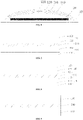
- the display apparatus of the present disclosure includes a substrate 10, a display device 20 and a thin-film encapsulation structure.
- the display device 20 is an organic light-emitting diode.
- the thin-film encapsulation structure is arranged at one side of the display device 20 away from the substrate 10, configured to package this display device 20.
- the thin-film encapsulation structure includes a first inorganic film layer 110, a first organic film layer 210, a second inorganic film layer 120 and a second organic film layer 220 which are laminated sequentially from inside to outside.
- the thin-film encapsulation structure in this example includes a first inorganic film layer 110, a first organic film layer 210 and a second inorganic film layer 120 which are laminated sequentially at one side of the organic light-emitting diode from inside to outside.
- the first inorganic film layer 110 has sequentially from inside to outside a first sub-layer 111 of the first inorganic film layer and a second sub-layer 112 of the first inorganic film layer which are made of silicon nitride.
- the first sub-layer 111 of the first inorganic film layer has a refractive index of 1.78, and a thickness of 200 nm
- the second sub-layer 112 of the first inorganic film layer has a refractive index of 1.85, and a thickness of 800 nm.
- the second inorganic film layer 120 has sequentially from inside to outside a first sub-layer 121 of the second inorganic film layer and a second sub-layer 122 of the second inorganic film layer which are made of silicon nitride.
- the first sub-layer 121 of the second inorganic film layer and the second sub-layer 122 of the second inorganic film layer have refractive indexes of 1.79 and 1.85 respectively, and thicknesses of 200 nm and 800 nm respectively.
- the display apparatus packaged by the thin-film encapsulation structure in this example is measured under a test condition of a high temperature at 60 °C and a high humidity at 90H that the storage life is more than 760h.
- the thin-film encapsulation structure in this example includes a first inorganic film layer 110, a first organic film layer 210 and a second inorganic film layer 120 which are laminated at one side of the organic light-emitting diode sequentially from inside to outside.
- the first inorganic film layer 110 has sequentially from inside to outside a first sub-layer 111 of the first inorganic film layer, a second sub-layer 112 of the first inorganic film layer and a third sub-layer 113 of the first inorganic film layer which are made of silicon nitride.
- the first sub-layer 111 of the first inorganic film layer, the second sub-layer 112 of the first inorganic film layer, and the third sub-layer 113 of the first inorganic film layer have refractive indexes of 1.76, 1.83, and 1.85 respectively, and thicknesses of 100 nm, 400 nm, and 500 nm respectively.
- the second inorganic film layer 120 has sequentially from inside to outside a first sub-layer 121 of the second inorganic film layer, a second sub-layer 122 of the second inorganic film layer and a third sub-layer 123 of the second inorganic film layer which are made of silicon nitride.
- the first sub-layer 121 of the second inorganic film layer, the second sub-layer 122 of the second inorganic film layer, and the third sub-layer 123 of the second inorganic film layer have refractive indexes of 1.76, 1.83, and 1.87 respectively, and thicknesses of 100 nm, 400 nm, and 500 nm respectively.
- the display apparatus packaged by the thin-film encapsulation structure of this example is measured under a test condition at 60 °C and at 90H that the storage life is 870h.
- the thin-film encapsulation structure of this example includes a first inorganic film layer, a first organic film layer and a second inorganic film layer which are laminated at one side of the organic light-emitting diode sequentially from inside to outside.
- the first inorganic film layer has sequentially from inside to outside a first sub-layer of the first inorganic film layer, a second sub-layer of the first inorganic film layer and a third sub-layer of the first inorganic film layer which are made of silicon nitride.
- the first sub-layer of the first inorganic film layer, the second sub-layer of the first inorganic film layer, and the third sub-layer of the first inorganic film layer have refractive indexes of 1.76, 1.83, and 1.85 respectively, and thicknesses of 200 nm, 500 nm, and 600 nm respectively.
- the second inorganic film layer is a sub-layer having a uniform refractive index, which is made of silicon nitride.
- the second inorganic film layer has a refractive index of 1.87 and a thickness of 1000 nm.
- the display apparatus packaged by the thin-film encapsulation structure of this example is measured under a test condition of a high temperature at 60 °C and a high humidity at 90H that the storage life is more than 760h.
- the thin-film encapsulation structure of this example includes a first inorganic film layer, a first organic film layer and a second inorganic film layer which are laminated at one side of the organic light-emitting diode sequentially from inside to outside.
- the first inorganic film layer has sequentially from inside to outside a first sub-layer of the first inorganic film layer and a second sub-layer of the first inorganic film layer which are made of silicon nitride.
- the first sub-layer of the first inorganic film layer and the second sub-layer of the first inorganic film layer have refractive indexes of 1.76 and 1.80 respectively, and thicknesses of 500 nm and 600 nm respectively.
- the second inorganic film layer has sequentially from inside to outside a first sub-layer of the second inorganic film layer and a second sub-layer of the second inorganic film layer which are made of silicon nitride.
- the first sub-layer of the second inorganic film layer and the second sub-layer of the second inorganic film layer have refractive indexes of 1.83 and 1.87 respectively, and thicknesses of 500 nm, 600 nm respectively.
- the display apparatus packaged by the thin-film encapsulation structure of this example is measured under a test condition of a high temperature at 60 °C and a high humidity at 90H that the storage life is more than 760h.
- the thin-film encapsulation structure in this comparative example includes a first inorganic film layer 110, a first organic film layer 210 and a second inorganic film layer 120 which are laminated at one side of the organic light-emitting diode sequentially from inside to outside.
- the first inorganic film layer 110 is an inorganic film layer having a uniform refractive index, which is made of silicon nitride.
- the first inorganic film layer 110 has a uniform refractive index of 1.78, and a thickness of 1,000 nm which is equal to the thickness of the first inorganic film layer in the example 1.
- the second inorganic film layer 120 is an inorganic film layer having a uniform refractive index, which is made of silicon nitride.
- the second inorganic film layer 120 has a uniform refractive index of 1.78, and a thickness of 1,000 nm which is equal to the thickness of the second inorganic film layer in the example 1.
- the display apparatus packaged by the thin-film encapsulation structure of this comparative example is measured under a test condition at 60 °C and at 90H that the storage life is 240h.
- the thin-film encapsulation structure in this comparative example includes a first inorganic film layer, a first organic film layer and a second inorganic film layer which are laminated at one side of the organic light-emitting diode sequentially from inside to outside.
- the first inorganic film layer has sequentially from inside to outside a first sub-layer of the first inorganic film layer and a second sub-layer of the first inorganic film layer which are made of silicon nitride.
- the first sub-layer of the first inorganic film layer and the second sub-layer of the first inorganic film layer have refractive indexes of 1.85 and 1.78 respectively, and thicknesses of 200 nm and 800 nm respectively.
- the second inorganic film layer has sequentially from inside to outside a first sub-layer of the second inorganic film layer and a second sub-layer of the second inorganic film layer which are made of silicon nitride.
- the first sub-layer of the second inorganic film layer and the second sub-layer of the second inorganic film layer have refractive indexes of 1.85 and 1.79 respectively, and thicknesses of 200 nm and 800 nm respectively.
- the display apparatus packaged by the thin-film encapsulation structure of this comparative example is measured under a test condition at 60 °C and at 90H that the storage life is 350h.
- the thin-film encapsulation structure in this comparative example includes a first inorganic film layer, a first organic film layer and a second inorganic film layer which are laminated at one side of the organic light-emitting diode sequentially from inside to outside.
- the first inorganic film layer has sequentially from inside to outside a first sub-layer of the first inorganic film layer, a second sub-layer of the first inorganic film layer and a third sub-layer of the first inorganic film layer which are made of silicon nitride.
- the first sub-layer of the first inorganic film layer, the second sub-layer of the first inorganic film layer, and the third sub-layer of the first inorganic film layer have refractive indexes are of 1.85, 1.83, and 1.76 respectively, and thicknesses of 200 nm, 500 nm, 600 nm respectively.
- the second inorganic film layer is a sub-layer having a uniform refractive index, which is made of silicon nitride.
- the second inorganic film layer has a refractive index of 1.87 and a thickness of 1000 nm.
- the display apparatus packaged by the thin-film encapsulation structure of this comparative example is measured under a test condition at 60 °C and at 90H that the storage life is 380h.
- the thin-film encapsulation structure in this comparative example includes a first inorganic film layer, a first organic film layer and a second inorganic film layer which are laminated at one side of the organic light-emitting diode sequentially from inside to outside.
- the first inorganic film layer has sequentially from inside to outside a first sub-layer of the first inorganic film layer and a second sub-layer of the first inorganic film layer which are made of silicon nitride.
- the first sub-layer of the first inorganic film layer and the second sub-layer of the first inorganic film layer have refractive indexes of 1.80 and 1.76 respectively, and thicknesses of 600 nm and 500 nm respectively.
- the second inorganic film layer has sequentially from inside to outside a first sub-layer of the second inorganic film layer and a second sub-layer of the second inorganic film layer which are made of silicon nitride.
- the first sub-layer of the second inorganic film layer and the second sub-layer of the second inorganic film layer have refractive indexes of 1.87 and 1.83 respectively, and thicknesses of 600 nm and 500 nm respectively.
- the display apparatus packaged by the thin-film encapsulation structure of this example is measured under a test condition of a high temperature at 60 °C and a high humidity at 90H that the storage life is 380h.
- the thin-film encapsulation structure according to the present disclosure have sub-layers with gradually increasing refractive indexes in the case of the same package thickness, so that the density of the inorganic film layer can be increased. Accordingly, as the refractive indexes of the sub-layers are increased gradually, stresses of the sub-layers are reduced sub-layer by sub-layer, which can significantly improve the moisture and oxygen barrier capabilities of the product, and improve the storage life of the product.
- first and second are used merely for illustrative purposes and are not to be construed as indicating or implying relative importance.
Landscapes
- Inorganic Chemistry (AREA)
- Chemical & Material Sciences (AREA)
- Engineering & Computer Science (AREA)
- Physics & Mathematics (AREA)
- Power Engineering (AREA)
- General Physics & Mathematics (AREA)
- Condensed Matter Physics & Semiconductors (AREA)
- Computer Hardware Design (AREA)
- Microelectronics & Electronic Packaging (AREA)
- Optics & Photonics (AREA)
- Manufacturing & Machinery (AREA)
- Electroluminescent Light Sources (AREA)
- Laminated Bodies (AREA)
- Devices For Indicating Variable Information By Combining Individual Elements (AREA)
Applications Claiming Priority (2)
| Application Number | Priority Date | Filing Date | Title |
|---|---|---|---|
| CN201710752001.5A CN109427992B (zh) | 2017-08-28 | 2017-08-28 | 薄膜封装结构及具有其的显示装置 |
| PCT/CN2018/085172 WO2019041866A1 (zh) | 2017-08-28 | 2018-04-28 | 薄膜封装结构及具有其的显示装置 |
Publications (3)
| Publication Number | Publication Date |
|---|---|
| EP3557645A1 EP3557645A1 (en) | 2019-10-23 |
| EP3557645A4 EP3557645A4 (en) | 2020-03-04 |
| EP3557645B1 true EP3557645B1 (en) | 2022-12-07 |
Family
ID=63960618
Family Applications (1)
| Application Number | Title | Priority Date | Filing Date |
|---|---|---|---|
| EP18849544.4A Active EP3557645B1 (en) | 2017-08-28 | 2018-04-28 | Film packaging structure and display apparatus having same |
Country Status (7)
| Country | Link |
|---|---|
| US (1) | US11251402B2 (enExample) |
| EP (1) | EP3557645B1 (enExample) |
| JP (1) | JP6873249B2 (enExample) |
| KR (1) | KR102263856B1 (enExample) |
| CN (1) | CN109427992B (enExample) |
| TW (1) | TWI695462B (enExample) |
| WO (1) | WO2019041866A1 (enExample) |
Families Citing this family (10)
| Publication number | Priority date | Publication date | Assignee | Title |
|---|---|---|---|---|
| CN109103222A (zh) * | 2018-08-20 | 2018-12-28 | 武汉华星光电半导体显示技术有限公司 | 一种oled显示面板以及显示装置 |
| CN111384282B (zh) * | 2018-12-27 | 2021-10-01 | Tcl科技集团股份有限公司 | 封装薄膜及其制备方法和发光显示装置 |
| KR102785782B1 (ko) * | 2019-02-07 | 2025-03-24 | 삼성디스플레이 주식회사 | 양자점 색 변환 필터를 구비하는 유기발광 표시장치 |
| CN110048019A (zh) * | 2019-04-12 | 2019-07-23 | 深圳市华星光电半导体显示技术有限公司 | 柔性oled显示装置及制备方法 |
| CN110504382B (zh) * | 2019-08-26 | 2021-09-28 | 昆山国显光电有限公司 | 一种显示面板和显示装置 |
| CN110970572B (zh) * | 2019-11-14 | 2025-06-17 | 京东方科技集团股份有限公司 | 封装结构、显示面板及显示装置 |
| CN111224016A (zh) * | 2020-01-16 | 2020-06-02 | Oppo广东移动通信有限公司 | 封装膜层、显示屏及电子设备 |
| CN111785768A (zh) * | 2020-08-25 | 2020-10-16 | 京东方科技集团股份有限公司 | 有机发光显示面板、制备方法和显示装置 |
| CN112670331B (zh) * | 2020-12-24 | 2022-08-19 | 武汉天马微电子有限公司 | 一种有机发光显示面板及其封装层制备方法、显示装置 |
| CN115207241A (zh) * | 2021-04-08 | 2022-10-18 | 广东聚华印刷显示技术有限公司 | 封装结构及显示面板 |
Family Cites Families (30)
| Publication number | Priority date | Publication date | Assignee | Title |
|---|---|---|---|---|
| JPWO2005027582A1 (ja) * | 2003-09-10 | 2006-11-24 | 富士通株式会社 | 表示装置及びその製造方法 |
| US7202504B2 (en) | 2004-05-20 | 2007-04-10 | Semiconductor Energy Laboratory Co., Ltd. | Light-emitting element and display device |
| JP5124083B2 (ja) * | 2004-06-09 | 2013-01-23 | 三星ディスプレイ株式會社 | 有機電界発光表示装置及びその製造方法 |
| KR100615221B1 (ko) * | 2004-06-09 | 2006-08-25 | 삼성에스디아이 주식회사 | 유기 전계 발광 표시 장치 및 이의 제조 방법 |
| US7259055B2 (en) * | 2005-02-24 | 2007-08-21 | Sharp Laboratories Of America, Inc. | Method of forming high-luminescence silicon electroluminescence device |
| US7297642B2 (en) | 2005-02-14 | 2007-11-20 | Sharp Laboratories Of America, Inc. | Sputter-deposited rare earth element-doped silicon oxide film with silicon nanocrystals for electroluminescence applications |
| JP4887473B2 (ja) | 2005-06-30 | 2012-02-29 | エルジー ディスプレイ カンパニー リミテッド | 有機el素子及びそれを用いた有機elディスプレイ並びに有機elディスプレイの製造方法 |
| FR2936651B1 (fr) * | 2008-09-30 | 2011-04-08 | Commissariat Energie Atomique | Dispositif optoelectronique organique et son procede d'encapsulation. |
| JP2010244697A (ja) * | 2009-04-01 | 2010-10-28 | Seiko Epson Corp | 有機el装置、有機el装置の製造方法、電子機器 |
| CN101697343B (zh) | 2009-10-27 | 2011-06-15 | 苏州纳科显示技术有限公司 | 一种薄膜封装方法 |
| JP2012216452A (ja) | 2011-04-01 | 2012-11-08 | Hitachi High-Technologies Corp | 光半導体装置およびその製造方法 |
| WO2013065213A1 (ja) | 2011-11-02 | 2013-05-10 | パナソニック株式会社 | 有機発光パネルおよびその製造方法 |
| TWI429526B (zh) | 2011-12-15 | 2014-03-11 | Ind Tech Res Inst | 水氣阻障複合膜及封裝結構 |
| KR20140022683A (ko) | 2012-08-14 | 2014-02-25 | 삼성디스플레이 주식회사 | 유기 발광 장치 및 그 제조 방법 |
| KR102048926B1 (ko) | 2012-11-19 | 2019-11-27 | 삼성디스플레이 주식회사 | 유기 발광 표시 장치 및 이의 제조 방법 |
| KR102010849B1 (ko) * | 2012-12-26 | 2019-08-14 | 엘지디스플레이 주식회사 | 유기발광소자 |
| WO2015029608A1 (ja) * | 2013-08-28 | 2015-03-05 | シャープ株式会社 | エレクトロルミネッセンス装置、及びその製造方法 |
| KR20150052490A (ko) | 2013-11-06 | 2015-05-14 | 삼성디스플레이 주식회사 | 유기발광 표시장치 및 그 제조방법 |
| CN104750285B (zh) | 2013-12-27 | 2019-01-18 | 昆山工研院新型平板显示技术中心有限公司 | 一种触控显示装置及其制备方法 |
| TWI545827B (zh) | 2014-05-23 | 2016-08-11 | 群創光電股份有限公司 | 有機發光二極體顯示面板 |
| TWI565118B (zh) | 2014-11-25 | 2017-01-01 | 財團法人工業技術研究院 | 封裝膜材與電子元件封裝體 |
| EP3034548A1 (en) | 2014-12-18 | 2016-06-22 | Nederlandse Organisatie voor toegepast- natuurwetenschappelijk onderzoek TNO | Barrier film laminate comprising submicron getter particles and electronic device comprising such a laminate |
| KR20160082864A (ko) | 2014-12-29 | 2016-07-11 | 삼성디스플레이 주식회사 | 표시 장치 및 이의 제조 방법 |
| TWI570965B (zh) | 2015-02-26 | 2017-02-11 | 友達光電股份有限公司 | 發光裝置和顯示器 |
| CN106158905A (zh) | 2015-04-21 | 2016-11-23 | 上海和辉光电有限公司 | 发光器件结构及有机发光面板 |
| KR102407115B1 (ko) * | 2015-06-25 | 2022-06-09 | 삼성디스플레이 주식회사 | 유기 발광 표시 장치 |
| KR102201296B1 (ko) * | 2015-10-29 | 2021-01-08 | 엘지디스플레이 주식회사 | 플렉서블 유기발광다이오드 표시장치 및 그 제조 방법 |
| JP2017147191A (ja) * | 2016-02-19 | 2017-08-24 | 株式会社ジャパンディスプレイ | 表示装置、及び表示装置の製造方法 |
| CN106887530B (zh) | 2017-01-20 | 2019-06-21 | 南京国兆光电科技有限公司 | 一种有机电致发光器件的薄膜封装结构及制备方法 |
| CN106816462B (zh) * | 2017-03-28 | 2019-08-02 | 上海天马有机发光显示技术有限公司 | 有机发光二极管显示装置及制造方法 |
-
2017
- 2017-08-28 CN CN201710752001.5A patent/CN109427992B/zh active Active
-
2018
- 2018-04-28 EP EP18849544.4A patent/EP3557645B1/en active Active
- 2018-04-28 JP JP2019538433A patent/JP6873249B2/ja active Active
- 2018-04-28 US US16/328,734 patent/US11251402B2/en active Active
- 2018-04-28 KR KR1020197021219A patent/KR102263856B1/ko active Active
- 2018-04-28 WO PCT/CN2018/085172 patent/WO2019041866A1/zh not_active Ceased
- 2018-05-14 TW TW107116227A patent/TWI695462B/zh active
Also Published As
| Publication number | Publication date |
|---|---|
| KR102263856B1 (ko) | 2021-06-11 |
| EP3557645A4 (en) | 2020-03-04 |
| CN109427992B (zh) | 2019-10-18 |
| US20210336217A1 (en) | 2021-10-28 |
| TWI695462B (zh) | 2020-06-01 |
| JP6873249B2 (ja) | 2021-05-19 |
| KR20190092579A (ko) | 2019-08-07 |
| WO2019041866A1 (zh) | 2019-03-07 |
| JP2020505727A (ja) | 2020-02-20 |
| TW201830611A (zh) | 2018-08-16 |
| CN109427992A (zh) | 2019-03-05 |
| EP3557645A1 (en) | 2019-10-23 |
| US11251402B2 (en) | 2022-02-15 |
Similar Documents
| Publication | Publication Date | Title |
|---|---|---|
| EP3557645B1 (en) | Film packaging structure and display apparatus having same | |
| US8552634B2 (en) | Organic light-emitting display apparatus | |
| US8461760B1 (en) | Thin film encapsulation for flat panel display device and method of manufacturing thin film encapsulation structure | |
| CN1977404B (zh) | 扩散阻挡层和扩散阻挡层的制造方法 | |
| EP2838131B1 (en) | Organic light-emitting display apparatus and method of manufacturing the same | |
| US20160322600A1 (en) | Display module encapsulating structure and preparing method thereof | |
| CN106848088B (zh) | 显示模组封装结构及其制备方法 | |
| CN110571347B (zh) | 一种显示面板及其制备方法 | |
| WO2015085712A1 (zh) | 一种多功能封装膜及显示装置 | |
| WO2015085723A1 (zh) | 有机电致发光显示器件、其制备方法及显示装置 | |
| CN110391349B (zh) | 一种有机发光二极管显示面板及其制作方法 | |
| WO2019127677A1 (zh) | 一种oled薄膜封装结构及封装方法 | |
| WO2020206980A1 (zh) | 柔性oled显示装置及制备方法 | |
| US10454065B1 (en) | OLED device encapsulating method and structure, OLED device, and display screen | |
| US10707450B2 (en) | OLED thin film packaging structure and method | |
| WO2020029351A1 (zh) | 一种复合膜层及制作方法、oled显示面板的制作方法 | |
| CN111952479B (zh) | 柔性薄膜封装oled结构及制作方法 | |
| US11943954B2 (en) | Encapsulation structure and encapsulation method for flexible organic light-emitting diode device | |
| KR102350896B1 (ko) | 유기 발광 표시 장치 및 그 제조 방법 | |
| JPWO2013111218A1 (ja) | 素子構造体及び素子構造体の製造方法 | |
| KR20140111778A (ko) | 투명 가스 배리어성 필름 및 이를 제조하는 방법 |
Legal Events
| Date | Code | Title | Description |
|---|---|---|---|
| STAA | Information on the status of an ep patent application or granted ep patent |
Free format text: STATUS: THE INTERNATIONAL PUBLICATION HAS BEEN MADE |
|
| PUAI | Public reference made under article 153(3) epc to a published international application that has entered the european phase |
Free format text: ORIGINAL CODE: 0009012 |
|
| STAA | Information on the status of an ep patent application or granted ep patent |
Free format text: STATUS: REQUEST FOR EXAMINATION WAS MADE |
|
| 17P | Request for examination filed |
Effective date: 20190718 |
|
| AK | Designated contracting states |
Kind code of ref document: A1 Designated state(s): AL AT BE BG CH CY CZ DE DK EE ES FI FR GB GR HR HU IE IS IT LI LT LU LV MC MK MT NL NO PL PT RO RS SE SI SK SM TR |
|
| AX | Request for extension of the european patent |
Extension state: BA ME |
|
| A4 | Supplementary search report drawn up and despatched |
Effective date: 20200130 |
|
| RIC1 | Information provided on ipc code assigned before grant |
Ipc: H01L 51/50 20060101AFI20200124BHEP Ipc: H01L 51/52 20060101ALI20200124BHEP |
|
| STAA | Information on the status of an ep patent application or granted ep patent |
Free format text: STATUS: EXAMINATION IS IN PROGRESS |
|
| 17Q | First examination report despatched |
Effective date: 20201016 |
|
| DAV | Request for validation of the european patent (deleted) | ||
| DAX | Request for extension of the european patent (deleted) | ||
| GRAP | Despatch of communication of intention to grant a patent |
Free format text: ORIGINAL CODE: EPIDOSNIGR1 |
|
| STAA | Information on the status of an ep patent application or granted ep patent |
Free format text: STATUS: GRANT OF PATENT IS INTENDED |
|
| INTG | Intention to grant announced |
Effective date: 20220830 |
|
| GRAS | Grant fee paid |
Free format text: ORIGINAL CODE: EPIDOSNIGR3 |
|
| GRAA | (expected) grant |
Free format text: ORIGINAL CODE: 0009210 |
|
| STAA | Information on the status of an ep patent application or granted ep patent |
Free format text: STATUS: THE PATENT HAS BEEN GRANTED |
|
| REG | Reference to a national code |
Ref country code: DE Ref legal event code: R079 Ref document number: 602018044075 Country of ref document: DE Free format text: PREVIOUS MAIN CLASS: H01L0051500000 Ipc: H10K0050000000 |
|
| AK | Designated contracting states |
Kind code of ref document: B1 Designated state(s): AL AT BE BG CH CY CZ DE DK EE ES FI FR GB GR HR HU IE IS IT LI LT LU LV MC MK MT NL NO PL PT RO RS SE SI SK SM TR |
|
| REG | Reference to a national code |
Ref country code: GB Ref legal event code: FG4D |
|
| REG | Reference to a national code |
Ref country code: CH Ref legal event code: EP Ref country code: AT Ref legal event code: REF Ref document number: 1536824 Country of ref document: AT Kind code of ref document: T Effective date: 20221215 |
|
| REG | Reference to a national code |
Ref country code: DE Ref legal event code: R096 Ref document number: 602018044075 Country of ref document: DE |
|
| REG | Reference to a national code |
Ref country code: IE Ref legal event code: FG4D |
|
| REG | Reference to a national code |
Ref country code: LT Ref legal event code: MG9D |
|
| REG | Reference to a national code |
Ref country code: NL Ref legal event code: MP Effective date: 20221207 |
|
| PG25 | Lapsed in a contracting state [announced via postgrant information from national office to epo] |
Ref country code: SE Free format text: LAPSE BECAUSE OF FAILURE TO SUBMIT A TRANSLATION OF THE DESCRIPTION OR TO PAY THE FEE WITHIN THE PRESCRIBED TIME-LIMIT Effective date: 20221207 Ref country code: NO Free format text: LAPSE BECAUSE OF FAILURE TO SUBMIT A TRANSLATION OF THE DESCRIPTION OR TO PAY THE FEE WITHIN THE PRESCRIBED TIME-LIMIT Effective date: 20230307 Ref country code: LT Free format text: LAPSE BECAUSE OF FAILURE TO SUBMIT A TRANSLATION OF THE DESCRIPTION OR TO PAY THE FEE WITHIN THE PRESCRIBED TIME-LIMIT Effective date: 20221207 Ref country code: FI Free format text: LAPSE BECAUSE OF FAILURE TO SUBMIT A TRANSLATION OF THE DESCRIPTION OR TO PAY THE FEE WITHIN THE PRESCRIBED TIME-LIMIT Effective date: 20221207 Ref country code: ES Free format text: LAPSE BECAUSE OF FAILURE TO SUBMIT A TRANSLATION OF THE DESCRIPTION OR TO PAY THE FEE WITHIN THE PRESCRIBED TIME-LIMIT Effective date: 20221207 |
|
| REG | Reference to a national code |
Ref country code: AT Ref legal event code: MK05 Ref document number: 1536824 Country of ref document: AT Kind code of ref document: T Effective date: 20221207 |
|
| PG25 | Lapsed in a contracting state [announced via postgrant information from national office to epo] |
Ref country code: RS Free format text: LAPSE BECAUSE OF FAILURE TO SUBMIT A TRANSLATION OF THE DESCRIPTION OR TO PAY THE FEE WITHIN THE PRESCRIBED TIME-LIMIT Effective date: 20221207 Ref country code: PL Free format text: LAPSE BECAUSE OF FAILURE TO SUBMIT A TRANSLATION OF THE DESCRIPTION OR TO PAY THE FEE WITHIN THE PRESCRIBED TIME-LIMIT Effective date: 20221207 Ref country code: LV Free format text: LAPSE BECAUSE OF FAILURE TO SUBMIT A TRANSLATION OF THE DESCRIPTION OR TO PAY THE FEE WITHIN THE PRESCRIBED TIME-LIMIT Effective date: 20221207 Ref country code: HR Free format text: LAPSE BECAUSE OF FAILURE TO SUBMIT A TRANSLATION OF THE DESCRIPTION OR TO PAY THE FEE WITHIN THE PRESCRIBED TIME-LIMIT Effective date: 20221207 Ref country code: GR Free format text: LAPSE BECAUSE OF FAILURE TO SUBMIT A TRANSLATION OF THE DESCRIPTION OR TO PAY THE FEE WITHIN THE PRESCRIBED TIME-LIMIT Effective date: 20230308 |
|
| PG25 | Lapsed in a contracting state [announced via postgrant information from national office to epo] |
Ref country code: NL Free format text: LAPSE BECAUSE OF FAILURE TO SUBMIT A TRANSLATION OF THE DESCRIPTION OR TO PAY THE FEE WITHIN THE PRESCRIBED TIME-LIMIT Effective date: 20221207 |
|
| P01 | Opt-out of the competence of the unified patent court (upc) registered |
Effective date: 20230526 |
|
| PG25 | Lapsed in a contracting state [announced via postgrant information from national office to epo] |
Ref country code: SM Free format text: LAPSE BECAUSE OF FAILURE TO SUBMIT A TRANSLATION OF THE DESCRIPTION OR TO PAY THE FEE WITHIN THE PRESCRIBED TIME-LIMIT Effective date: 20221207 Ref country code: RO Free format text: LAPSE BECAUSE OF FAILURE TO SUBMIT A TRANSLATION OF THE DESCRIPTION OR TO PAY THE FEE WITHIN THE PRESCRIBED TIME-LIMIT Effective date: 20221207 Ref country code: PT Free format text: LAPSE BECAUSE OF FAILURE TO SUBMIT A TRANSLATION OF THE DESCRIPTION OR TO PAY THE FEE WITHIN THE PRESCRIBED TIME-LIMIT Effective date: 20230410 Ref country code: EE Free format text: LAPSE BECAUSE OF FAILURE TO SUBMIT A TRANSLATION OF THE DESCRIPTION OR TO PAY THE FEE WITHIN THE PRESCRIBED TIME-LIMIT Effective date: 20221207 Ref country code: CZ Free format text: LAPSE BECAUSE OF FAILURE TO SUBMIT A TRANSLATION OF THE DESCRIPTION OR TO PAY THE FEE WITHIN THE PRESCRIBED TIME-LIMIT Effective date: 20221207 Ref country code: AT Free format text: LAPSE BECAUSE OF FAILURE TO SUBMIT A TRANSLATION OF THE DESCRIPTION OR TO PAY THE FEE WITHIN THE PRESCRIBED TIME-LIMIT Effective date: 20221207 |
|
| PG25 | Lapsed in a contracting state [announced via postgrant information from national office to epo] |
Ref country code: SK Free format text: LAPSE BECAUSE OF FAILURE TO SUBMIT A TRANSLATION OF THE DESCRIPTION OR TO PAY THE FEE WITHIN THE PRESCRIBED TIME-LIMIT Effective date: 20221207 Ref country code: IS Free format text: LAPSE BECAUSE OF FAILURE TO SUBMIT A TRANSLATION OF THE DESCRIPTION OR TO PAY THE FEE WITHIN THE PRESCRIBED TIME-LIMIT Effective date: 20230407 Ref country code: AL Free format text: LAPSE BECAUSE OF FAILURE TO SUBMIT A TRANSLATION OF THE DESCRIPTION OR TO PAY THE FEE WITHIN THE PRESCRIBED TIME-LIMIT Effective date: 20221207 |
|
| REG | Reference to a national code |
Ref country code: DE Ref legal event code: R097 Ref document number: 602018044075 Country of ref document: DE |
|
| PLBE | No opposition filed within time limit |
Free format text: ORIGINAL CODE: 0009261 |
|
| STAA | Information on the status of an ep patent application or granted ep patent |
Free format text: STATUS: NO OPPOSITION FILED WITHIN TIME LIMIT |
|
| PG25 | Lapsed in a contracting state [announced via postgrant information from national office to epo] |
Ref country code: DK Free format text: LAPSE BECAUSE OF FAILURE TO SUBMIT A TRANSLATION OF THE DESCRIPTION OR TO PAY THE FEE WITHIN THE PRESCRIBED TIME-LIMIT Effective date: 20221207 |
|
| 26N | No opposition filed |
Effective date: 20230908 |
|
| PG25 | Lapsed in a contracting state [announced via postgrant information from national office to epo] |
Ref country code: SI Free format text: LAPSE BECAUSE OF FAILURE TO SUBMIT A TRANSLATION OF THE DESCRIPTION OR TO PAY THE FEE WITHIN THE PRESCRIBED TIME-LIMIT Effective date: 20221207 |
|
| REG | Reference to a national code |
Ref country code: CH Ref legal event code: PL |
|
| PG25 | Lapsed in a contracting state [announced via postgrant information from national office to epo] |
Ref country code: LU Free format text: LAPSE BECAUSE OF NON-PAYMENT OF DUE FEES Effective date: 20230428 |
|
| REG | Reference to a national code |
Ref country code: BE Ref legal event code: MM Effective date: 20230430 |
|
| PG25 | Lapsed in a contracting state [announced via postgrant information from national office to epo] |
Ref country code: MC Free format text: LAPSE BECAUSE OF FAILURE TO SUBMIT A TRANSLATION OF THE DESCRIPTION OR TO PAY THE FEE WITHIN THE PRESCRIBED TIME-LIMIT Effective date: 20221207 |
|
| PG25 | Lapsed in a contracting state [announced via postgrant information from national office to epo] |
Ref country code: MC Free format text: LAPSE BECAUSE OF FAILURE TO SUBMIT A TRANSLATION OF THE DESCRIPTION OR TO PAY THE FEE WITHIN THE PRESCRIBED TIME-LIMIT Effective date: 20221207 Ref country code: LI Free format text: LAPSE BECAUSE OF NON-PAYMENT OF DUE FEES Effective date: 20230430 Ref country code: CH Free format text: LAPSE BECAUSE OF NON-PAYMENT OF DUE FEES Effective date: 20230430 |
|
| REG | Reference to a national code |
Ref country code: IE Ref legal event code: MM4A |
|
| PG25 | Lapsed in a contracting state [announced via postgrant information from national office to epo] |
Ref country code: BE Free format text: LAPSE BECAUSE OF NON-PAYMENT OF DUE FEES Effective date: 20230430 |
|
| PG25 | Lapsed in a contracting state [announced via postgrant information from national office to epo] |
Ref country code: IE Free format text: LAPSE BECAUSE OF NON-PAYMENT OF DUE FEES Effective date: 20230428 |
|
| PG25 | Lapsed in a contracting state [announced via postgrant information from national office to epo] |
Ref country code: IE Free format text: LAPSE BECAUSE OF NON-PAYMENT OF DUE FEES Effective date: 20230428 |
|
| PG25 | Lapsed in a contracting state [announced via postgrant information from national office to epo] |
Ref country code: IT Free format text: LAPSE BECAUSE OF FAILURE TO SUBMIT A TRANSLATION OF THE DESCRIPTION OR TO PAY THE FEE WITHIN THE PRESCRIBED TIME-LIMIT Effective date: 20221207 |
|
| PG25 | Lapsed in a contracting state [announced via postgrant information from national office to epo] |
Ref country code: BG Free format text: LAPSE BECAUSE OF FAILURE TO SUBMIT A TRANSLATION OF THE DESCRIPTION OR TO PAY THE FEE WITHIN THE PRESCRIBED TIME-LIMIT Effective date: 20221207 |
|
| PG25 | Lapsed in a contracting state [announced via postgrant information from national office to epo] |
Ref country code: BG Free format text: LAPSE BECAUSE OF FAILURE TO SUBMIT A TRANSLATION OF THE DESCRIPTION OR TO PAY THE FEE WITHIN THE PRESCRIBED TIME-LIMIT Effective date: 20221207 |
|
| PGFP | Annual fee paid to national office [announced via postgrant information from national office to epo] |
Ref country code: DE Payment date: 20250411 Year of fee payment: 8 |
|
| PGFP | Annual fee paid to national office [announced via postgrant information from national office to epo] |
Ref country code: GB Payment date: 20250417 Year of fee payment: 8 |
|
| PGFP | Annual fee paid to national office [announced via postgrant information from national office to epo] |
Ref country code: FR Payment date: 20250429 Year of fee payment: 8 |
|
| PG25 | Lapsed in a contracting state [announced via postgrant information from national office to epo] |
Ref country code: CY Free format text: LAPSE BECAUSE OF FAILURE TO SUBMIT A TRANSLATION OF THE DESCRIPTION OR TO PAY THE FEE WITHIN THE PRESCRIBED TIME-LIMIT; INVALID AB INITIO Effective date: 20180428 |
|
| PG25 | Lapsed in a contracting state [announced via postgrant information from national office to epo] |
Ref country code: HU Free format text: LAPSE BECAUSE OF FAILURE TO SUBMIT A TRANSLATION OF THE DESCRIPTION OR TO PAY THE FEE WITHIN THE PRESCRIBED TIME-LIMIT; INVALID AB INITIO Effective date: 20180428 |