EP3549249B1 - Variable voltage generator circuit, capacitor and method - Google Patents
Variable voltage generator circuit, capacitor and method Download PDFInfo
- Publication number
- EP3549249B1 EP3549249B1 EP17808423.2A EP17808423A EP3549249B1 EP 3549249 B1 EP3549249 B1 EP 3549249B1 EP 17808423 A EP17808423 A EP 17808423A EP 3549249 B1 EP3549249 B1 EP 3549249B1
- Authority
- EP
- European Patent Office
- Prior art keywords
- converter
- voltage
- capacitor
- circuit
- input capacitor
- Prior art date
- Legal status (The legal status is an assumption and is not a legal conclusion. Google has not performed a legal analysis and makes no representation as to the accuracy of the status listed.)
- Active
Links
Images



Classifications
-
- H—ELECTRICITY
- H02—GENERATION; CONVERSION OR DISTRIBUTION OF ELECTRIC POWER
- H02M—APPARATUS FOR CONVERSION BETWEEN AC AND AC, BETWEEN AC AND DC, OR BETWEEN DC AND DC, AND FOR USE WITH MAINS OR SIMILAR POWER SUPPLY SYSTEMS; CONVERSION OF DC OR AC INPUT POWER INTO SURGE OUTPUT POWER; CONTROL OR REGULATION THEREOF
- H02M3/00—Conversion of DC power input into DC power output
- H02M3/22—Conversion of DC power input into DC power output with intermediate conversion into AC
- H02M3/24—Conversion of DC power input into DC power output with intermediate conversion into AC by static converters
- H02M3/28—Conversion of DC power input into DC power output with intermediate conversion into AC by static converters using discharge tubes with control electrode or semiconductor devices with control electrode to produce the intermediate AC
- H02M3/325—Conversion of DC power input into DC power output with intermediate conversion into AC by static converters using discharge tubes with control electrode or semiconductor devices with control electrode to produce the intermediate AC using devices of a triode or a transistor type requiring continuous application of a control signal
- H02M3/335—Conversion of DC power input into DC power output with intermediate conversion into AC by static converters using discharge tubes with control electrode or semiconductor devices with control electrode to produce the intermediate AC using devices of a triode or a transistor type requiring continuous application of a control signal using semiconductor devices only
- H02M3/33569—Conversion of DC power input into DC power output with intermediate conversion into AC by static converters using discharge tubes with control electrode or semiconductor devices with control electrode to produce the intermediate AC using devices of a triode or a transistor type requiring continuous application of a control signal using semiconductor devices only having several active switching elements
- H02M3/33576—Conversion of DC power input into DC power output with intermediate conversion into AC by static converters using discharge tubes with control electrode or semiconductor devices with control electrode to produce the intermediate AC using devices of a triode or a transistor type requiring continuous application of a control signal using semiconductor devices only having several active switching elements having at least one active switching element at the secondary side of an isolation transformer
- H02M3/33584—Bidirectional converters
-
- H—ELECTRICITY
- H01—ELECTRIC ELEMENTS
- H01J—ELECTRIC DISCHARGE TUBES OR DISCHARGE LAMPS
- H01J37/00—Discharge tubes with provision for introducing objects or material to be exposed to the discharge, e.g. for the purpose of examination or processing thereof
- H01J37/32—Gas-filled discharge tubes
- H01J37/32009—Arrangements for generation of plasma specially adapted for examination or treatment of objects, e.g. plasma sources
- H01J37/32082—Radio frequency generated discharge
- H01J37/32174—Circuits specially adapted for controlling the RF discharge
-
- H—ELECTRICITY
- H02—GENERATION; CONVERSION OR DISTRIBUTION OF ELECTRIC POWER
- H02M—APPARATUS FOR CONVERSION BETWEEN AC AND AC, BETWEEN AC AND DC, OR BETWEEN DC AND DC, AND FOR USE WITH MAINS OR SIMILAR POWER SUPPLY SYSTEMS; CONVERSION OF DC OR AC INPUT POWER INTO SURGE OUTPUT POWER; CONTROL OR REGULATION THEREOF
- H02M1/00—Details of apparatus for conversion
- H02M1/0067—Converter structures employing plural converter units, other than for parallel operation of the units on a single load
- H02M1/007—Plural converter units in cascade
-
- H—ELECTRICITY
- H02—GENERATION; CONVERSION OR DISTRIBUTION OF ELECTRIC POWER
- H02M—APPARATUS FOR CONVERSION BETWEEN AC AND AC, BETWEEN AC AND DC, OR BETWEEN DC AND DC, AND FOR USE WITH MAINS OR SIMILAR POWER SUPPLY SYSTEMS; CONVERSION OF DC OR AC INPUT POWER INTO SURGE OUTPUT POWER; CONTROL OR REGULATION THEREOF
- H02M1/00—Details of apparatus for conversion
- H02M1/42—Circuits or arrangements for compensating for or adjusting power factor in converters or inverters
- H02M1/4208—Arrangements for improving power factor of AC input
- H02M1/4225—Arrangements for improving power factor of AC input using a non-isolated boost converter
-
- H—ELECTRICITY
- H02—GENERATION; CONVERSION OR DISTRIBUTION OF ELECTRIC POWER
- H02M—APPARATUS FOR CONVERSION BETWEEN AC AND AC, BETWEEN AC AND DC, OR BETWEEN DC AND DC, AND FOR USE WITH MAINS OR SIMILAR POWER SUPPLY SYSTEMS; CONVERSION OF DC OR AC INPUT POWER INTO SURGE OUTPUT POWER; CONTROL OR REGULATION THEREOF
- H02M3/00—Conversion of DC power input into DC power output
- H02M3/02—Conversion of DC power input into DC power output without intermediate conversion into AC
- H02M3/04—Conversion of DC power input into DC power output without intermediate conversion into AC by static converters
- H02M3/10—Conversion of DC power input into DC power output without intermediate conversion into AC by static converters using discharge tubes with control electrode or semiconductor devices with control electrode
- H02M3/145—Conversion of DC power input into DC power output without intermediate conversion into AC by static converters using discharge tubes with control electrode or semiconductor devices with control electrode using devices of a triode or transistor type requiring continuous application of a control signal
- H02M3/155—Conversion of DC power input into DC power output without intermediate conversion into AC by static converters using discharge tubes with control electrode or semiconductor devices with control electrode using devices of a triode or transistor type requiring continuous application of a control signal using semiconductor devices only
- H02M3/156—Conversion of DC power input into DC power output without intermediate conversion into AC by static converters using discharge tubes with control electrode or semiconductor devices with control electrode using devices of a triode or transistor type requiring continuous application of a control signal using semiconductor devices only with automatic control of output voltage or current, e.g. switching regulators
- H02M3/158—Conversion of DC power input into DC power output without intermediate conversion into AC by static converters using discharge tubes with control electrode or semiconductor devices with control electrode using devices of a triode or transistor type requiring continuous application of a control signal using semiconductor devices only with automatic control of output voltage or current, e.g. switching regulators including plural semiconductor devices as final control devices for a single load
-
- H—ELECTRICITY
- H02—GENERATION; CONVERSION OR DISTRIBUTION OF ELECTRIC POWER
- H02N—ELECTRIC MACHINES NOT OTHERWISE PROVIDED FOR
- H02N2/00—Electric machines in general using piezoelectric effect, electrostriction or magnetostriction
- H02N2/02—Electric machines in general using piezoelectric effect, electrostriction or magnetostriction producing linear motion, e.g. actuators; Linear positioners ; Linear motors
- H02N2/06—Drive circuits; Control arrangements or methods
- H02N2/065—Large signal circuits, e.g. final stages
-
- Y—GENERAL TAGGING OF NEW TECHNOLOGICAL DEVELOPMENTS; GENERAL TAGGING OF CROSS-SECTIONAL TECHNOLOGIES SPANNING OVER SEVERAL SECTIONS OF THE IPC; TECHNICAL SUBJECTS COVERED BY FORMER USPC CROSS-REFERENCE ART COLLECTIONS [XRACs] AND DIGESTS
- Y02—TECHNOLOGIES OR APPLICATIONS FOR MITIGATION OR ADAPTATION AGAINST CLIMATE CHANGE
- Y02B—CLIMATE CHANGE MITIGATION TECHNOLOGIES RELATED TO BUILDINGS, e.g. HOUSING, HOUSE APPLIANCES OR RELATED END-USER APPLICATIONS
- Y02B70/00—Technologies for an efficient end-user side electric power management and consumption
- Y02B70/10—Technologies improving the efficiency by using switched-mode power supplies [SMPS], i.e. efficient power electronics conversion e.g. power factor correction or reduction of losses in power supplies or efficient standby modes
Definitions
- the invention relates to the field of high-voltage, fast variable DC voltage source.
- it relates to the field of providing fast dynamic high- voltage DC control voltages to devices which present a capacitive load, but which consume little or no energy.
- variable power capacitor which can be used to provide a highly dynamic RF power supply, such as may be required for plasma chambers used for plasma etching or deposition, for example.
- the variable power capacitor has a paraelectric dielectric material with a variable permittivity which may be varied by applying a large electric field or a large DC voltage across the dielectric material.
- Control electrodes are provided for this purpose. By varying the voltage on the control electrodes, it is possible to change the capacitance of the variable capacitor very fast and accurately. This in turn permits a highly responsive impedance matching of the radiofrequency (RF) power supply to a plasma processing chamber, which in turn improves control and feature resolution of the plasma process (eg etching or deposition process).
- RF radiofrequency
- a DC power supply comprising an auxiliary converter applied for steering the charge from an offline storage element is used.
- the auxiliary converter allows the main DC-DC converter energy storage to be relatively small, yet allowing the system to deal with sudden changes in supply current caused by pulsing.
- US 2015/048718 describes a capacitive actuator connected to an output of an apparatus which is formed with a capacitor connected between an input and a reference potential, with a full bridge with four power switching elements connected in parallel with the capacitor.
- a control circuit first turns on the first and third power switching elements. Current then flows from the first capacitor via a coil connected between the bridge paths and energy is stored in the coil. When a maximum current value is reached, the first and third power switching elements are switched off and magnetic energy stored in the coil decays due to current flow via the diodes of the second and fourth power switching elements. This charges the capacitive actuator.
- the capacitive actuator is charged to a predefined voltage by possible repeated switching of the first and third power switching elements.
- the applied DC voltage should advantageously be capable of being varied between a high voltage (for example more than 1kV, more than 3kV, or more than 5kV) and a low voltage (eg 0V) very quickly (eg within 10ms, or 1ms or 100ps, or 10 ps or less), ie at a high rate of as much as 10 5 V/s or more, or 10 6 V/s or more, or 10 7 V/s or more, or 10 8 V/s or more.
- a high voltage for example more than 1kV, more than 3kV, or more than 5kV
- a low voltage eg 0V
- control electrodes, and the dielectric between them, form a load capacitance for the applied DC voltage, so the control voltage source should preferably be capable of charging or discharging the load capacitance through the full voltage range (eg from 0V to 5kV or vice versa) in this short time.
- piezo-actuators can be used in applications such as high-speed switching. Accelerations of 10000g or more can be achieved if the applied driver voltage can be varied quickly enough. To this end, the driver voltage may need to be varied through a large voltage range (eg 1kV or more) in a very short time (eg 1ms or less, or 0.1ms or less, or 0.01ms or less).
- a large voltage range eg 1kV or more
- a very short time eg 1ms or less, or 0.1ms or less, or 0.01ms or less.
- the capacitance of a capacitive load such as that presented by a piezo actuator or by the dielectric between the control electrodes of the variable power capacitor mentioned above may be of the order of 10pF to 100nF, or more than 100nF, for example. It is a non- trivial task to charge and discharge such a capacitive load with large voltage ranges when the charge/discharge time is very short. The problem is further compounded by any lossy elements in the control voltage generator circuitry. In applications such as the fast variable capacitor for plasma generation or the piezo actuators described above, it is advantageous to be able to vary the output voltage not only very rapidly, but also with a high precision.
- a two-stage power converter is known from US20110090717 , in which an unregulated LLC converter is controlled by pulse-width modulating a buck-boost converter to adjust an input voltage of the LLC converter using feedback from the output voltage of the LLC converter, such that the output is maintained at a constant voltage such as 400V from an input voltage of 140V.
- the circuit is designed to provide smooth power with constant input and output voltages and with an energy transfer between the input and output which is as efficient as possible, because the circuit is required to work for example at 2500W.
- the circuit described in US20110090717 is a large and robust circuit comprising components dimensioned to sustain operation at the specified high working power ratings, and the circuit would not be suitable for generating rapidly and precisely variable output voltages from 0V to eg 5kV or higher, with negligible net power consumption (ie with very high power efficiency), as specified for the applications described above.
- the circuit of US20110090717 would not be capable of generating an output voltage range which included very low voltages, approaching 0V.
- the present invention aims to overcome at least some of the above disadvantages of prior art variable control voltage generation circuits.
- a variable voltage generator circuit according to the invention is described in claim 1
- a variable capacitor according to the invention is described in claim 9
- a method according to the invention is described in claim 10.
- Variants of the circuit and method of the invention are described in dependent claims 2-8 and 11 to 13.
- a bidirectional DC-DC converter is used to vary the output voltage by varying its voltage amplification factor while keeping the input voltage more or less steady.
- An input capacitor provides a reservoir of charge which can be used to charge the capacitive load when the control input signal determines that the output voltage is to be increased, and the load capacitance is discharged back to the input capacitor when the output voltage is to be decreased. The charge is thus transferred back and forth to charge and discharge the load capacitance as required by the particular application (eg the dielectric between the control electrodes of a variable power capacitor used for supplying power to a plasma chamber).
- the circuit thus has low overall losses, because most of the electrical energy is recovered whenever the output voltage is to be decreased.
- the circuit can be implemented with relatively small components, and it means that the control input signal can be used to accurately and rapidly set the value for generating the desired instantaneous output voltage. Furthermore, the amplified output voltage follows the control input signal without the need for any further control inputs, such as feedback from the output voltage.
- the steering signal which may be a pulse width modulation signal applied to the switching control of the buck-boost converter
- the circuit allows charge to move between the upstream input capacitance and the downstream load capacitance, with low losses, such that the overall power consumption of the voltage supply circuit is substantially limited to only the losses.
- the instantaneous power transfer in the circuit may sometimes be large, particularly during large, fast output voltage swings, the large current values are transient and the circuit components need only be dimensioned for very modest overall power transfer. Because the variable capacitor (or the piezo actuator) draws very little (eg substantially zero) net power, the overall net power transfer through the voltage supply circuit is very low, ie substantially zero.
- the components of the input circuit also referred to as the top-up circuit, need only be dimensioned to supply enough power for this net power requirement, and to compensate for losses incurred as the current flows back and forth between the upstream and downstream capacitances.
- a variable capacitor 1 such as that known from WO2016034241A1 is illustrated schematically in figure 1 .
- the example capacitor 1 comprises a block or plate of paraelectric dielectric material 7 and two main capacitor electrodes 5 and capacitor leads 4.
- the capacitance of the device can be varied by applying an electric field across the dielectric 7. This can be achieved by connecting a variable voltage source V c to control electrodes 6 at connection terminals 2 and 3. Varying the control voltage V c causes the permittivity of the part of the dielectric 7 between the control electrodes 6 to vary, thus altering the capacitance of the capacitor 1 between the capacitor electrodes 5.
- variable capacitor It is a significant advantage of this kind of variable capacitor that the capacitance can be varied very rapidly. This makes the capacitor useful for applications such as plasma generation, in which highly responsive impedance matching is required which can be achieved by fast adjustment of such kinds of variable capacitors by changing the applied high voltage.
- a suitable control voltage generator circuit is required, which is capable of providing the large voltage range, varying from low or zero voltage to high voltage (eg 1kV, 3kV, 5kV, or up to 6kV or more), and the high speed required.
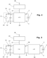
- Figures 2 to 6 show, in various levels of detail, schematic views of an example voltage supply circuit according to the invention, designed to fulfill the requirements described above for supplying a rapidly-variable high voltage for the control electrodes of the variable capacitor described.
- an input capacitor 12 on the upstream (left) side of the circuit is maintained charged at supply voltage V Cin (voltage at circuit node 17) by DC voltage source 11 at V s via diode 15.
- the circuit 10 is designed to charge the input capacitor 12 to voltage V s when the voltage V Cin on the capacitor falls below V s .
- This "top-up" charging of the input capacitor 12 replenishes electrical energy which is lost due to losses which arise when charge is moved back and forth by the bidirectional DC-DC converter circuit 20 between the input capacitor and the load capacitance 1.
- V Cin is normally equal to or a little higher than V s , depending on the circuit components and the application requirements.
- V Cin will be greater than V s when the input capacitor is already at Vs and is to be charged using charge from the load capacitance 1.
- the input capacitor 12 is advantageously selected to have a capacitance much greater than that of the load capacitance 1, so that even a sudden large decrease in V c will only require a modest increase of V Cin above V s in order to charge the input capacitor 12 with the charge returning from the load capacitance.
- the input capacitance 12 may preferably have a capacitance value of at least 50 times, or more preferably at least 100 times, or more preferably 200 times, or more preferably 500 times the capacitance value of the load capacitance 1, for example.
- the load capacitance is substantially purely capacitive (it may have a reactance which is at least 100 times as great as its resistance, for example).
- the bidirectional DC-DC converter circuit 20 has a variable voltage amplification factor G which is controlled by control input signal 27 from control unit 25.
- the term voltage conversion factor is taken to refer to the instantaneous voltage amplification provided by the DC-DC converter 20 in the forward (ie upstream-to-downstream, left-to-right, input-to-output) direction.
- the voltage conversion factor in the reverse direction is similar to the forward conversion factor, but in the inverse (reciprocal) sense.
- Control unit 25 may be required to translate a control input 26, which may indicate an instantaneous requirement of the application (eg a plasma chamber), into a control input signal 27 for setting the appropriate value of G for outputting the required output voltage V c .
- the control unit 25 may include some detailed application data (for example stored as algorithms or in fast look-up-table form) for mapping an instruction 26 into a suitable value of G for carrying out the instruction 26.
- the matchbox may call for the capacitor 1 to change capacitance suddenly from a first given value to a second, quite different value.
- control unit may be provided with data for calculating or otherwise determining what new value of V c is required in order to effect the new capacitance of the variable capacitor 1, and what value of G is required in order to change the output voltage V c to this new value.
- the required value of G is then encoded into control input signal 27 and used to change the voltage conversion factor of the DC-DC converter, whereupon a flow of charge takes place between input capacitor 12 and load capacitance 1, depending on whether the output voltage V c is to be increased or decreased.
- the capacitance between the control electrodes 6 may be the same as, or different from the capacitance between the principal electrodes 5, depending on the construction of the capacitor.
- Figure 3 shows an example variant of the circuit of figure 2 .
- the variable bidirectional DC-DC converter 20 is implemented as two converter stages 28 and 30, both of which are bidirectional, and which together perform the same function as the DC-DC converter circuit 20 of figure 2 .
- Variable bidirectional DC-DC circuit 28 generates a variable steering voltage with a conversion factor g determined by the control input signal 27.
- Constant bidirectional DC-DC converter circuit 30 has a constant voltage conversion factor K, where g x K is equivalent to the factor G of the circuit of figure 2 .
- the control unit 25 is not shown in figures 4 to 6 , but is assumed to be present in order to actuate at least some of the switches or switchable components in the detailed circuits of figures 4 to 6 .
- the control unit controls the switching components of the buck- boost converter 28, for example.
- the switching of the LLC converter preferably does not require any variable or programmed control, since it preferably operates with a substantially constant switching regime.
- FIG. 4 shows an example implementation of the circuit of figure 3 .
- a buck-boost converter 28 comprising switching elements 21, 22, an inductor 23 and capacitor 24 serves to generate a steering voltage V P at circuit node 29.
- Steering voltage V P is set by varying a switching duty cycle of the switching elements 21 and 22 under control of the control input signal (not shown).
- the instantaneous value of V P may be thought of as being proportional to V Cin multiplied by the "on" fraction of the duty cycle of the upper switching means 21.
- buck-boost converter acts as a buck converter in the forward direction (reducing the voltage V Cin to V P ) and as a boost converter in the reverse direction (amplifying the voltage V P to V Cin ).
- the steering voltage V P can be varied from a low or substantially zero value to a high value, substantially V Cin .
- the minimum of V p , V P (min) is preferably less than 25% of V Cin , or more preferably less than 10% of V n.
- the maximum of V p , V P (max) is preferably greater than 75% of V Cin , or more preferably greater than 90% of V Cin .
- variable capacitor 1 described above, for example, would typically have its greatest capacitance value when the control voltage V c is zero. In this case, it is advantageous to be able to reduce V P , and thereby V c , to 0V in order to maximise the available capacitance value of the variable capacitor 1.
- a single buck-boost converter circuit 28 is shown in figures 4 to 6 . However, two or more such circuits could be connected in parallel in order to distribute power over multiple interleaved slices and in order to reduce an amount of ripple or fluctuation in the value of V P .
- the values of the inductor 23 and the capacitor 24 are preferably small, in order to permit fast operation (eg 150 kHz or more), so the capacitor 24 does not provide a significant smoothing function.
- the constant DC-DC converter (represented as block 30 in Figures 3 to 6 ) may have a voltage amplification factor of 10 or more, in which case a ripple in V P may be magnified tenfold in V c . Interleaving multiple buck-boost converter circuit slices can help to mitigate such ripple in the output Vc.
- the bidirectional DC-DC converter 30 is implemented as a bidirectional synchronous resonant LLC converter as shown in figures 5 and 6 , having a substantially constant switching regime and predetermined voltage amplification characteristics, operating in a synchronous, soft-switched mode at or near the converter's resonant frequency.
- the amplification characteristics may be substantially linear or non-linear, but the transfer function should preferably be stable and predictable.
- the downstream voltage V c of the DC-DC converter 30 need not be used as a control parameter for controlling the buck-boost converter 28, as will be explained below.
- the control voltage generator circuit shown in figures 4 to 6 is controlled by one or more control units (not shown), which may be implemented in hardware and/or software.
- a control unit provides a pulse-width modulation (PWM) control signal to the bidirectional (buck-boost) converter circuit 28.
- PWM pulse-width modulation
- the control unit for providing the buck-boost control signal may calculate the PWM duty ratio based on parameters of the particular application for which the control voltage generator circuit is used.
- a control unit of the impedance matching apparatus may issue a capacitance value parameter instruction for the capacitor 1.
- the buck- boost control signal can be calculated which will result in the required capacitance value of the capacitor 1, taking into account different operating conditions (eg temperature).
- a similar control path can be implemented in that the buck- boost control signal can be calculated based on previously-obtained performance information mapping PWM duty cycle values to the resulting physical behaviour parameters of the actuator, under different operating conditions (eg temperature, humidity, physical load type etc).
- the switching elements are shown in figures 4 to 6 variously as symbolic switches or as silicon-based MOSFET transistors.
- the elements shown as switches may for example be implemented as MOSFETs or Gallium Nitride (GaN) transistors or Silicon Carbide (SiC) transistors if actively switched, or as diodes or diode-connected transistors if operating synchronously with other switched components.
- the DC-DC converter 30 shown in figure 6 may be configured such that the downstream side rectification circuit comprises soft- switched transistors 34 and 35, while the upstream side rectification circuit (shown as transistors 36, 37, 38, 39) comprises simple diodes or diode-connected transistors. In this case, the upstream side rectification circuit follows the switching of the downstream side circuit synchronously, as a slave arrangement.
- the DC-DC converter circuit 30 may advantageously operate synchronously, and preferably at a substantially constant operating (switching) frequency.
- the bidirectional converter circuit 28 may also be configured to operate at a substantially constant switching frequency. This frequency may be different from the operating frequency of the DC-DC converter circuit 30, or it may be selected to the same as the operating frequency of the DC-DC converter circuit 30.
- the latter variant has the advantage of reducing ripple in VP, and may mean that the capacitor 24 is not required at all, or only as a small component, since in this case energy can be transferred back and forth synchronously between the input capacitor 12 and load capacitor 1.
- FIG. 6 shows an implementation of the input circuit 10 using a power factor correction (PFC) circuit to generate a constant supply voltage V s from a range of input voltages applied to input 16.
- Capacitor 12 at the output of the PFC (10) may advantageously be a large capacitor capable of storing a big charge which moves back and forth through the circuit during dynamic operation when the output voltage V c changes significantly.
- Such capacitors could for example include electrolytic or/and specialized foil capacitors.
- the input circuit 10 may be constructed using components with a much lower power rating than would be needed for delivering the total amount of power delivered to the load capacitance 1.
- the power rating of the input circuit 10 may for example be lower than 15% of the quantity (C x f x U 2 ), where C is the load capacitance, f is the operating frequency of the converter circuit 20, and U is the maximum permitted voltage swing within one switching cycle of the converter circuit 20.
- the various operating parameters may be for example in the following ranges:
- the operating parameters may be for example:
- the operating parameters may be for example:
- the operating parameters may be for example:
- control voltage generator circuit of the invention has been described above with reference to two example applications of a capacitor 1 and a piezo actuator.
- the circuit can be used in other applications, in particular applications which require high efficiency (low net power consumption), high voltage, and high speed operation with a fast control response.
Landscapes
- Engineering & Computer Science (AREA)
- Power Engineering (AREA)
- Physics & Mathematics (AREA)
- Plasma & Fusion (AREA)
- Chemical & Material Sciences (AREA)
- Analytical Chemistry (AREA)
- Dc-Dc Converters (AREA)
Applications Claiming Priority (2)
| Application Number | Priority Date | Filing Date | Title |
|---|---|---|---|
| EP16201548 | 2016-11-30 | ||
| PCT/EP2017/080888 WO2018100014A1 (en) | 2016-11-30 | 2017-11-29 | Variable voltage generator circuit, capacitor and method |
Publications (2)
| Publication Number | Publication Date |
|---|---|
| EP3549249A1 EP3549249A1 (en) | 2019-10-09 |
| EP3549249B1 true EP3549249B1 (en) | 2024-02-14 |
Family
ID=57442598
Family Applications (1)
| Application Number | Title | Priority Date | Filing Date |
|---|---|---|---|
| EP17808423.2A Active EP3549249B1 (en) | 2016-11-30 | 2017-11-29 | Variable voltage generator circuit, capacitor and method |
Country Status (7)
| Country | Link |
|---|---|
| US (1) | US11496059B2 (https=) |
| EP (1) | EP3549249B1 (https=) |
| JP (1) | JP7065850B2 (https=) |
| KR (1) | KR102423387B1 (https=) |
| CN (1) | CN110291707B (https=) |
| TW (1) | TWI738930B (https=) |
| WO (1) | WO2018100014A1 (https=) |
Families Citing this family (9)
| Publication number | Priority date | Publication date | Assignee | Title |
|---|---|---|---|---|
| CN109460104B (zh) * | 2018-12-03 | 2020-11-06 | 惠科股份有限公司 | 一种电压调节电路、电压调节装置以及显示装置 |
| CN110208583B (zh) * | 2019-05-06 | 2022-02-18 | 福建星云电子股份有限公司 | 一种基于电芯充放电的涟波电流发生装置 |
| TWI688847B (zh) * | 2019-07-16 | 2020-03-21 | 致茂電子股份有限公司 | 電壓維持電路 |
| CN112242704B (zh) * | 2019-07-16 | 2023-09-29 | 致茂电子(苏州)有限公司 | 电压维持电路 |
| US11133784B2 (en) * | 2019-12-10 | 2021-09-28 | xMEMS Labs, Inc. | Method of driving circuit with energy recycle capability |
| DE102019135497B4 (de) * | 2019-12-20 | 2021-11-11 | Nova Plasma Ltd | Piezoelektrischer Plasmagenerator und Verfahren zum Betrieb eines piezoelektrischen Plasmagenerators |
| US20230087705A1 (en) * | 2021-09-21 | 2023-03-23 | Apple Inc. | Integrated standby power supply |
| US20240014728A1 (en) * | 2022-07-08 | 2024-01-11 | Holding Zero, LLC | Bidirectional buck-boost controller |
| US11961684B1 (en) * | 2023-08-02 | 2024-04-16 | King Faisal University | Energy storage in a minimized variable capacitance system using capacitor with distance-movable plates |
Citations (1)
| Publication number | Priority date | Publication date | Assignee | Title |
|---|---|---|---|---|
| US20150048718A1 (en) * | 2012-03-22 | 2015-02-19 | Continental Automotive Gmbh | Method for operating a capacitive actuator |
Family Cites Families (25)
| Publication number | Priority date | Publication date | Assignee | Title |
|---|---|---|---|---|
| KR100521120B1 (ko) * | 1998-02-13 | 2005-10-12 | 가부시끼가이샤 히다치 세이사꾸쇼 | 반도체소자의 표면처리방법 및 장치 |
| JP3232511B2 (ja) | 1999-03-23 | 2001-11-26 | 株式会社ハイデン研究所 | 高周波高圧電源 |
| CN1241316C (zh) | 1999-07-13 | 2006-02-08 | 东京电子株式会社 | 产生感性耦合的等离子的射频电源 |
| JP4468840B2 (ja) * | 2005-02-25 | 2010-05-26 | 三菱電機株式会社 | 電力変換装置 |
| TWI362817B (en) * | 2007-11-27 | 2012-04-21 | Upi Semiconductor Corp | Dc/dc converters and related methods |
| FR2925789A1 (fr) * | 2007-12-20 | 2009-06-26 | Commissariat Energie Atomique | Convertisseur electrique a capacite variable |
| JP4743222B2 (ja) * | 2008-04-25 | 2011-08-10 | ソニー株式会社 | 可変容量素子及び、電子機器 |
| FR2937479B1 (fr) * | 2008-10-21 | 2010-10-29 | Schneider Toshiba Inverter | Dispositif de recuperation d'energie dans un variateur de vitesse |
| KR101031217B1 (ko) | 2009-10-21 | 2011-04-27 | 주식회사 오리엔트전자 | 고정 시비율로 동작하는 llc 공진 컨버터를 사용한 2단 방식 절연형 양방향 dc/dc 전력변환기 |
| CN102598468A (zh) * | 2010-09-10 | 2012-07-18 | 松下电器产业株式会社 | 电力控制装置、电力控制方法及电力供给系统 |
| JP5785710B2 (ja) * | 2010-12-14 | 2015-09-30 | ローム株式会社 | Dc/dcコンバータならびにそれを用いた電源装置および電子機器 |
| US9762115B2 (en) | 2011-02-03 | 2017-09-12 | Viswa N. Sharma | Bidirectional multimode power converter |
| JP5673168B2 (ja) * | 2011-02-08 | 2015-02-18 | 富士電機株式会社 | 電力変換装置 |
| JP5877648B2 (ja) * | 2011-03-23 | 2016-03-08 | 北陸電力株式会社 | 分散型電源システム |
| US9155156B2 (en) * | 2011-07-06 | 2015-10-06 | Allegro Microsystems, Llc | Electronic circuits and techniques for improving a short duty cycle behavior of a DC-DC converter driving a load |
| JP5432969B2 (ja) | 2011-10-31 | 2014-03-05 | シャープ株式会社 | Dc/dcコンバータ、ソーラー充電システム、及び移動体 |
| JP6292497B2 (ja) * | 2013-03-18 | 2018-03-14 | パナソニックIpマネジメント株式会社 | 電力変換器、パワーコンディショナ |
| CN105340166B (zh) * | 2013-07-11 | 2017-09-19 | 三菱电机株式会社 | Dc/dc变换器 |
| CN104638904B (zh) * | 2013-11-06 | 2018-01-19 | 意法半导体研发(深圳)有限公司 | 峰值电流模式dc‑dc转换器 |
| US20150174693A1 (en) | 2013-11-19 | 2015-06-25 | Aaron Astle | Welder With Active Linear DC Filtering Circuit |
| WO2015192133A2 (en) * | 2014-06-13 | 2015-12-17 | University Of Maryland | An integrated dual-output grid-to-vehicle (g2v) and vehicle-to-grid (v2g) onboard charger for plug-in electric vehicles |
| US11011350B2 (en) | 2014-09-04 | 2021-05-18 | Comet Ag | Variable power capacitor for RF power applications |
| US9419551B2 (en) * | 2014-09-17 | 2016-08-16 | Arm Limited | Motor driver and a method of operating thereof |
| DE102014016076A1 (de) | 2014-10-29 | 2015-08-13 | Audi Ag | DC/DC-Wandler für ein Kraftfahrzeug |
| US9627961B1 (en) * | 2015-12-11 | 2017-04-18 | National Chung Shan Institute Of Science And Technology | Mixed power supply device with a merging network switch |
-
2017
- 2017-11-29 JP JP2019528809A patent/JP7065850B2/ja active Active
- 2017-11-29 EP EP17808423.2A patent/EP3549249B1/en active Active
- 2017-11-29 KR KR1020197018618A patent/KR102423387B1/ko active Active
- 2017-11-29 WO PCT/EP2017/080888 patent/WO2018100014A1/en not_active Ceased
- 2017-11-29 CN CN201780073043.4A patent/CN110291707B/zh active Active
- 2017-11-29 US US16/465,415 patent/US11496059B2/en active Active
- 2017-11-29 TW TW106141679A patent/TWI738930B/zh active
Patent Citations (1)
| Publication number | Priority date | Publication date | Assignee | Title |
|---|---|---|---|---|
| US20150048718A1 (en) * | 2012-03-22 | 2015-02-19 | Continental Automotive Gmbh | Method for operating a capacitive actuator |
Non-Patent Citations (1)
| Title |
|---|
| HUANG LINA ET AL: "Analytical Switching Cycle Modeling of Bidirectional High-Voltage Flyback Converter for Capacitive Load Considering Core Loss Effect", IEEE TRANSACTIONS ON POWER ELECTRONICS, INSTITUTE OF ELECTRICAL AND ELECTRONICS ENGINEERS, USA, vol. 31, no. 1, 1 January 2016 (2016-01-01), pages 470 - 487, XP011669915, ISSN: 0885-8993, [retrieved on 20150921], DOI: 10.1109/TPEL.2015.2410796 * |
Also Published As
| Publication number | Publication date |
|---|---|
| TW201832038A (zh) | 2018-09-01 |
| JP2019537419A (ja) | 2019-12-19 |
| EP3549249A1 (en) | 2019-10-09 |
| KR20190089039A (ko) | 2019-07-29 |
| TWI738930B (zh) | 2021-09-11 |
| CN110291707B (zh) | 2022-04-29 |
| KR102423387B1 (ko) | 2022-07-20 |
| CN110291707A (zh) | 2019-09-27 |
| WO2018100014A1 (en) | 2018-06-07 |
| US20200007047A1 (en) | 2020-01-02 |
| JP7065850B2 (ja) | 2022-05-12 |
| US11496059B2 (en) | 2022-11-08 |
Similar Documents
| Publication | Publication Date | Title |
|---|---|---|
| EP3549249B1 (en) | Variable voltage generator circuit, capacitor and method | |
| CN104734509B (zh) | 用于功率转换器的系统和方法 | |
| KR101637650B1 (ko) | 직류-직류 변환기 | |
| US9929658B2 (en) | Controlling a switched mode power supply with maximised power efficiency | |
| US11967897B2 (en) | Suppression of rebalancing currents in a switched-capacitor network | |
| JP2019537419A5 (https=) | ||
| Qian et al. | Effect of combined output capacitors for stability of buck converters with constant on-time control | |
| US20040046527A1 (en) | Apparatus and method for charging and discharging a capacitor to a predetermined setpoint | |
| KR101804773B1 (ko) | 리플 제거 기능을 구비한 교류-직류 컨버터 회로 | |
| CN215452789U (zh) | 一种高升压比dc-dc升压电路 | |
| Kapat et al. | Null response to a large signal transient in an augmented dc-dc converter: A geometric approach | |
| KR101673662B1 (ko) | 직류-직류 변환기 | |
| Patmal et al. | A Modified V 2 Control Scheme For Load Rapid Transient Response with Nonlinear Control Feature of a Cascaded Pulsed Load Power Supply | |
| CN113489316A (zh) | 一种高升压比dc-dc升压电路 | |
| KR101971788B1 (ko) | 직류 배전 시스템 안정화 장치 | |
| Neyens et al. | Implementation of an augmented boost converter for improved load transient response | |
| Goudanaikar et al. | Interleaved High Step up Dc-Dc Converter with PID Controller | |
| Gu et al. | Using magnetic coupling to improve the bandwidth and phase margin of boost converters | |
| WO2014133188A1 (en) | Switching regulator | |
| KR20120003155A (ko) | Dc-dc 부스트 컨버터 회로와 그 구동 방법 | |
| JP4421479B2 (ja) | コンデンサをあらかじめ定めた設定ポイントまで充電および放電するための装置および方法 | |
| Steinke et al. | Control method and prototyping of the Multistage Stacked Boost Architecture (MSBA) | |
| Huang et al. | Energy Efficiency Investigation of Bidirectional High Voltage Flyback Converter for DEAP Actuator | |
| KR20150022579A (ko) | 전원 장치 |
Legal Events
| Date | Code | Title | Description |
|---|---|---|---|
| STAA | Information on the status of an ep patent application or granted ep patent |
Free format text: STATUS: UNKNOWN |
|
| STAA | Information on the status of an ep patent application or granted ep patent |
Free format text: STATUS: THE INTERNATIONAL PUBLICATION HAS BEEN MADE |
|
| PUAI | Public reference made under article 153(3) epc to a published international application that has entered the european phase |
Free format text: ORIGINAL CODE: 0009012 |
|
| STAA | Information on the status of an ep patent application or granted ep patent |
Free format text: STATUS: REQUEST FOR EXAMINATION WAS MADE |
|
| 17P | Request for examination filed |
Effective date: 20190701 |
|
| AK | Designated contracting states |
Kind code of ref document: A1 Designated state(s): AL AT BE BG CH CY CZ DE DK EE ES FI FR GB GR HR HU IE IS IT LI LT LU LV MC MK MT NL NO PL PT RO RS SE SI SK SM TR |
|
| AX | Request for extension of the european patent |
Extension state: BA ME |
|
| DAV | Request for validation of the european patent (deleted) | ||
| DAX | Request for extension of the european patent (deleted) | ||
| STAA | Information on the status of an ep patent application or granted ep patent |
Free format text: STATUS: EXAMINATION IS IN PROGRESS |
|
| 17Q | First examination report despatched |
Effective date: 20200312 |
|
| 17Q | First examination report despatched |
Effective date: 20200416 |
|
| RIC1 | Information provided on ipc code assigned before grant |
Ipc: H02N 2/06 20060101ALN20230731BHEP Ipc: H02M 3/158 20060101ALN20230731BHEP Ipc: H02M 1/42 20070101ALN20230731BHEP Ipc: H02M 1/00 20060101ALN20230731BHEP Ipc: H01J 37/32 20060101ALN20230731BHEP Ipc: H02M 3/335 20060101AFI20230731BHEP |
|
| RIC1 | Information provided on ipc code assigned before grant |
Ipc: H02N 2/06 20060101ALN20230813BHEP Ipc: H02M 3/158 20060101ALN20230813BHEP Ipc: H02M 1/42 20070101ALN20230813BHEP Ipc: H02M 1/00 20060101ALN20230813BHEP Ipc: H01J 37/32 20060101ALN20230813BHEP Ipc: H02M 3/335 20060101AFI20230813BHEP |
|
| GRAP | Despatch of communication of intention to grant a patent |
Free format text: ORIGINAL CODE: EPIDOSNIGR1 |
|
| STAA | Information on the status of an ep patent application or granted ep patent |
Free format text: STATUS: GRANT OF PATENT IS INTENDED |
|
| RIC1 | Information provided on ipc code assigned before grant |
Ipc: H02N 2/06 20060101ALN20230906BHEP Ipc: H02M 3/158 20060101ALN20230906BHEP Ipc: H02M 1/42 20070101ALN20230906BHEP Ipc: H02M 1/00 20060101ALN20230906BHEP Ipc: H01J 37/32 20060101ALN20230906BHEP Ipc: H02M 3/335 20060101AFI20230906BHEP |
|
| INTG | Intention to grant announced |
Effective date: 20230926 |
|
| P01 | Opt-out of the competence of the unified patent court (upc) registered |
Effective date: 20231017 |
|
| GRAS | Grant fee paid |
Free format text: ORIGINAL CODE: EPIDOSNIGR3 |
|
| GRAA | (expected) grant |
Free format text: ORIGINAL CODE: 0009210 |
|
| STAA | Information on the status of an ep patent application or granted ep patent |
Free format text: STATUS: THE PATENT HAS BEEN GRANTED |
|
| AK | Designated contracting states |
Kind code of ref document: B1 Designated state(s): AL AT BE BG CH CY CZ DE DK EE ES FI FR GB GR HR HU IE IS IT LI LT LU LV MC MK MT NL NO PL PT RO RS SE SI SK SM TR |
|
| REG | Reference to a national code |
Ref country code: GB Ref legal event code: FG4D |
|
| REG | Reference to a national code |
Ref country code: CH Ref legal event code: EP |
|
| REG | Reference to a national code |
Ref country code: DE Ref legal event code: R096 Ref document number: 602017079179 Country of ref document: DE |
|
| REG | Reference to a national code |
Ref country code: IE Ref legal event code: FG4D |
|
| REG | Reference to a national code |
Ref country code: LT Ref legal event code: MG9D |
|
| REG | Reference to a national code |
Ref country code: NL Ref legal event code: MP Effective date: 20240214 |
|
| PG25 | Lapsed in a contracting state [announced via postgrant information from national office to epo] |
Ref country code: IS Free format text: LAPSE BECAUSE OF FAILURE TO SUBMIT A TRANSLATION OF THE DESCRIPTION OR TO PAY THE FEE WITHIN THE PRESCRIBED TIME-LIMIT Effective date: 20240614 |
|
| PG25 | Lapsed in a contracting state [announced via postgrant information from national office to epo] |
Ref country code: LT Free format text: LAPSE BECAUSE OF FAILURE TO SUBMIT A TRANSLATION OF THE DESCRIPTION OR TO PAY THE FEE WITHIN THE PRESCRIBED TIME-LIMIT Effective date: 20240214 |
|
| PG25 | Lapsed in a contracting state [announced via postgrant information from national office to epo] |
Ref country code: GR Free format text: LAPSE BECAUSE OF FAILURE TO SUBMIT A TRANSLATION OF THE DESCRIPTION OR TO PAY THE FEE WITHIN THE PRESCRIBED TIME-LIMIT Effective date: 20240515 |
|
| REG | Reference to a national code |
Ref country code: AT Ref legal event code: MK05 Ref document number: 1657918 Country of ref document: AT Kind code of ref document: T Effective date: 20240214 |
|
| PG25 | Lapsed in a contracting state [announced via postgrant information from national office to epo] |
Ref country code: NL Free format text: LAPSE BECAUSE OF FAILURE TO SUBMIT A TRANSLATION OF THE DESCRIPTION OR TO PAY THE FEE WITHIN THE PRESCRIBED TIME-LIMIT Effective date: 20240214 Ref country code: HR Free format text: LAPSE BECAUSE OF FAILURE TO SUBMIT A TRANSLATION OF THE DESCRIPTION OR TO PAY THE FEE WITHIN THE PRESCRIBED TIME-LIMIT Effective date: 20240214 Ref country code: RS Free format text: LAPSE BECAUSE OF FAILURE TO SUBMIT A TRANSLATION OF THE DESCRIPTION OR TO PAY THE FEE WITHIN THE PRESCRIBED TIME-LIMIT Effective date: 20240514 |
|
| PG25 | Lapsed in a contracting state [announced via postgrant information from national office to epo] |
Ref country code: ES Free format text: LAPSE BECAUSE OF FAILURE TO SUBMIT A TRANSLATION OF THE DESCRIPTION OR TO PAY THE FEE WITHIN THE PRESCRIBED TIME-LIMIT Effective date: 20240214 |
|
| PG25 | Lapsed in a contracting state [announced via postgrant information from national office to epo] |
Ref country code: AT Free format text: LAPSE BECAUSE OF FAILURE TO SUBMIT A TRANSLATION OF THE DESCRIPTION OR TO PAY THE FEE WITHIN THE PRESCRIBED TIME-LIMIT Effective date: 20240214 |
|
| PG25 | Lapsed in a contracting state [announced via postgrant information from national office to epo] |
Ref country code: RS Free format text: LAPSE BECAUSE OF FAILURE TO SUBMIT A TRANSLATION OF THE DESCRIPTION OR TO PAY THE FEE WITHIN THE PRESCRIBED TIME-LIMIT Effective date: 20240514 Ref country code: NO Free format text: LAPSE BECAUSE OF FAILURE TO SUBMIT A TRANSLATION OF THE DESCRIPTION OR TO PAY THE FEE WITHIN THE PRESCRIBED TIME-LIMIT Effective date: 20240514 Ref country code: NL Free format text: LAPSE BECAUSE OF FAILURE TO SUBMIT A TRANSLATION OF THE DESCRIPTION OR TO PAY THE FEE WITHIN THE PRESCRIBED TIME-LIMIT Effective date: 20240214 Ref country code: LT Free format text: LAPSE BECAUSE OF FAILURE TO SUBMIT A TRANSLATION OF THE DESCRIPTION OR TO PAY THE FEE WITHIN THE PRESCRIBED TIME-LIMIT Effective date: 20240214 Ref country code: IS Free format text: LAPSE BECAUSE OF FAILURE TO SUBMIT A TRANSLATION OF THE DESCRIPTION OR TO PAY THE FEE WITHIN THE PRESCRIBED TIME-LIMIT Effective date: 20240614 Ref country code: HR Free format text: LAPSE BECAUSE OF FAILURE TO SUBMIT A TRANSLATION OF THE DESCRIPTION OR TO PAY THE FEE WITHIN THE PRESCRIBED TIME-LIMIT Effective date: 20240214 Ref country code: GR Free format text: LAPSE BECAUSE OF FAILURE TO SUBMIT A TRANSLATION OF THE DESCRIPTION OR TO PAY THE FEE WITHIN THE PRESCRIBED TIME-LIMIT Effective date: 20240515 Ref country code: FI Free format text: LAPSE BECAUSE OF FAILURE TO SUBMIT A TRANSLATION OF THE DESCRIPTION OR TO PAY THE FEE WITHIN THE PRESCRIBED TIME-LIMIT Effective date: 20240214 Ref country code: ES Free format text: LAPSE BECAUSE OF FAILURE TO SUBMIT A TRANSLATION OF THE DESCRIPTION OR TO PAY THE FEE WITHIN THE PRESCRIBED TIME-LIMIT Effective date: 20240214 Ref country code: BG Free format text: LAPSE BECAUSE OF FAILURE TO SUBMIT A TRANSLATION OF THE DESCRIPTION OR TO PAY THE FEE WITHIN THE PRESCRIBED TIME-LIMIT Effective date: 20240214 Ref country code: AT Free format text: LAPSE BECAUSE OF FAILURE TO SUBMIT A TRANSLATION OF THE DESCRIPTION OR TO PAY THE FEE WITHIN THE PRESCRIBED TIME-LIMIT Effective date: 20240214 |
|
| PG25 | Lapsed in a contracting state [announced via postgrant information from national office to epo] |
Ref country code: PT Free format text: LAPSE BECAUSE OF FAILURE TO SUBMIT A TRANSLATION OF THE DESCRIPTION OR TO PAY THE FEE WITHIN THE PRESCRIBED TIME-LIMIT Effective date: 20240614 Ref country code: PL Free format text: LAPSE BECAUSE OF FAILURE TO SUBMIT A TRANSLATION OF THE DESCRIPTION OR TO PAY THE FEE WITHIN THE PRESCRIBED TIME-LIMIT Effective date: 20240214 |
|
| PG25 | Lapsed in a contracting state [announced via postgrant information from national office to epo] |
Ref country code: SE Free format text: LAPSE BECAUSE OF FAILURE TO SUBMIT A TRANSLATION OF THE DESCRIPTION OR TO PAY THE FEE WITHIN THE PRESCRIBED TIME-LIMIT Effective date: 20240214 Ref country code: PT Free format text: LAPSE BECAUSE OF FAILURE TO SUBMIT A TRANSLATION OF THE DESCRIPTION OR TO PAY THE FEE WITHIN THE PRESCRIBED TIME-LIMIT Effective date: 20240614 Ref country code: PL Free format text: LAPSE BECAUSE OF FAILURE TO SUBMIT A TRANSLATION OF THE DESCRIPTION OR TO PAY THE FEE WITHIN THE PRESCRIBED TIME-LIMIT Effective date: 20240214 Ref country code: LV Free format text: LAPSE BECAUSE OF FAILURE TO SUBMIT A TRANSLATION OF THE DESCRIPTION OR TO PAY THE FEE WITHIN THE PRESCRIBED TIME-LIMIT Effective date: 20240214 |
|
| PG25 | Lapsed in a contracting state [announced via postgrant information from national office to epo] |
Ref country code: DK Free format text: LAPSE BECAUSE OF FAILURE TO SUBMIT A TRANSLATION OF THE DESCRIPTION OR TO PAY THE FEE WITHIN THE PRESCRIBED TIME-LIMIT Effective date: 20240214 |
|
| PG25 | Lapsed in a contracting state [announced via postgrant information from national office to epo] |
Ref country code: SM Free format text: LAPSE BECAUSE OF FAILURE TO SUBMIT A TRANSLATION OF THE DESCRIPTION OR TO PAY THE FEE WITHIN THE PRESCRIBED TIME-LIMIT Effective date: 20240214 |
|
| PG25 | Lapsed in a contracting state [announced via postgrant information from national office to epo] |
Ref country code: EE Free format text: LAPSE BECAUSE OF FAILURE TO SUBMIT A TRANSLATION OF THE DESCRIPTION OR TO PAY THE FEE WITHIN THE PRESCRIBED TIME-LIMIT Effective date: 20240214 Ref country code: CZ Free format text: LAPSE BECAUSE OF FAILURE TO SUBMIT A TRANSLATION OF THE DESCRIPTION OR TO PAY THE FEE WITHIN THE PRESCRIBED TIME-LIMIT Effective date: 20240214 |
|
| PG25 | Lapsed in a contracting state [announced via postgrant information from national office to epo] |
Ref country code: SK Free format text: LAPSE BECAUSE OF FAILURE TO SUBMIT A TRANSLATION OF THE DESCRIPTION OR TO PAY THE FEE WITHIN THE PRESCRIBED TIME-LIMIT Effective date: 20240214 |
|
| PG25 | Lapsed in a contracting state [announced via postgrant information from national office to epo] |
Ref country code: SM Free format text: LAPSE BECAUSE OF FAILURE TO SUBMIT A TRANSLATION OF THE DESCRIPTION OR TO PAY THE FEE WITHIN THE PRESCRIBED TIME-LIMIT Effective date: 20240214 Ref country code: SK Free format text: LAPSE BECAUSE OF FAILURE TO SUBMIT A TRANSLATION OF THE DESCRIPTION OR TO PAY THE FEE WITHIN THE PRESCRIBED TIME-LIMIT Effective date: 20240214 Ref country code: RO Free format text: LAPSE BECAUSE OF FAILURE TO SUBMIT A TRANSLATION OF THE DESCRIPTION OR TO PAY THE FEE WITHIN THE PRESCRIBED TIME-LIMIT Effective date: 20240214 Ref country code: EE Free format text: LAPSE BECAUSE OF FAILURE TO SUBMIT A TRANSLATION OF THE DESCRIPTION OR TO PAY THE FEE WITHIN THE PRESCRIBED TIME-LIMIT Effective date: 20240214 Ref country code: DK Free format text: LAPSE BECAUSE OF FAILURE TO SUBMIT A TRANSLATION OF THE DESCRIPTION OR TO PAY THE FEE WITHIN THE PRESCRIBED TIME-LIMIT Effective date: 20240214 Ref country code: CZ Free format text: LAPSE BECAUSE OF FAILURE TO SUBMIT A TRANSLATION OF THE DESCRIPTION OR TO PAY THE FEE WITHIN THE PRESCRIBED TIME-LIMIT Effective date: 20240214 |
|
| REG | Reference to a national code |
Ref country code: DE Ref legal event code: R097 Ref document number: 602017079179 Country of ref document: DE |
|
| PG25 | Lapsed in a contracting state [announced via postgrant information from national office to epo] |
Ref country code: IT Free format text: LAPSE BECAUSE OF FAILURE TO SUBMIT A TRANSLATION OF THE DESCRIPTION OR TO PAY THE FEE WITHIN THE PRESCRIBED TIME-LIMIT Effective date: 20240214 |
|
| PLBE | No opposition filed within time limit |
Free format text: ORIGINAL CODE: 0009261 |
|
| STAA | Information on the status of an ep patent application or granted ep patent |
Free format text: STATUS: NO OPPOSITION FILED WITHIN TIME LIMIT |
|
| PG25 | Lapsed in a contracting state [announced via postgrant information from national office to epo] |
Ref country code: IT Free format text: LAPSE BECAUSE OF FAILURE TO SUBMIT A TRANSLATION OF THE DESCRIPTION OR TO PAY THE FEE WITHIN THE PRESCRIBED TIME-LIMIT Effective date: 20240214 |
|
| 26N | No opposition filed |
Effective date: 20241115 |
|
| PG25 | Lapsed in a contracting state [announced via postgrant information from national office to epo] |
Ref country code: SI Free format text: LAPSE BECAUSE OF FAILURE TO SUBMIT A TRANSLATION OF THE DESCRIPTION OR TO PAY THE FEE WITHIN THE PRESCRIBED TIME-LIMIT Effective date: 20240214 |
|
| PG25 | Lapsed in a contracting state [announced via postgrant information from national office to epo] |
Ref country code: MC Free format text: LAPSE BECAUSE OF FAILURE TO SUBMIT A TRANSLATION OF THE DESCRIPTION OR TO PAY THE FEE WITHIN THE PRESCRIBED TIME-LIMIT Effective date: 20240214 |
|
| PG25 | Lapsed in a contracting state [announced via postgrant information from national office to epo] |
Ref country code: LU Free format text: LAPSE BECAUSE OF NON-PAYMENT OF DUE FEES Effective date: 20241129 |
|
| REG | Reference to a national code |
Ref country code: BE Ref legal event code: MM Effective date: 20241130 |
|
| PG25 | Lapsed in a contracting state [announced via postgrant information from national office to epo] |
Ref country code: BE Free format text: LAPSE BECAUSE OF NON-PAYMENT OF DUE FEES Effective date: 20241130 |
|
| PG25 | Lapsed in a contracting state [announced via postgrant information from national office to epo] |
Ref country code: IE Free format text: LAPSE BECAUSE OF NON-PAYMENT OF DUE FEES Effective date: 20241129 |
|
| REG | Reference to a national code |
Ref country code: CH Ref legal event code: U11 Free format text: ST27 STATUS EVENT CODE: U-0-0-U10-U11 (AS PROVIDED BY THE NATIONAL OFFICE) Effective date: 20251201 |
|
| PGFP | Annual fee paid to national office [announced via postgrant information from national office to epo] |
Ref country code: DE Payment date: 20251117 Year of fee payment: 9 |
|
| PGFP | Annual fee paid to national office [announced via postgrant information from national office to epo] |
Ref country code: GB Payment date: 20251120 Year of fee payment: 9 |
|
| PGFP | Annual fee paid to national office [announced via postgrant information from national office to epo] |
Ref country code: FR Payment date: 20251120 Year of fee payment: 9 |
|
| PGFP | Annual fee paid to national office [announced via postgrant information from national office to epo] |
Ref country code: CH Payment date: 20251201 Year of fee payment: 9 |
|
| PG25 | Lapsed in a contracting state [announced via postgrant information from national office to epo] |
Ref country code: HU Free format text: LAPSE BECAUSE OF FAILURE TO SUBMIT A TRANSLATION OF THE DESCRIPTION OR TO PAY THE FEE WITHIN THE PRESCRIBED TIME-LIMIT; INVALID AB INITIO Effective date: 20171129 |
|
| PG25 | Lapsed in a contracting state [announced via postgrant information from national office to epo] |
Ref country code: CY Free format text: LAPSE BECAUSE OF FAILURE TO SUBMIT A TRANSLATION OF THE DESCRIPTION OR TO PAY THE FEE WITHIN THE PRESCRIBED TIME-LIMIT; INVALID AB INITIO Effective date: 20171129 |