EP3540794B1 - Light-emitting device - Google Patents
Light-emitting device Download PDFInfo
- Publication number
- EP3540794B1 EP3540794B1 EP19172258.6A EP19172258A EP3540794B1 EP 3540794 B1 EP3540794 B1 EP 3540794B1 EP 19172258 A EP19172258 A EP 19172258A EP 3540794 B1 EP3540794 B1 EP 3540794B1
- Authority
- EP
- European Patent Office
- Prior art keywords
- light
- emitting element
- fluorescent
- emitting device
- support body
- Prior art date
- Legal status (The legal status is an assumption and is not a legal conclusion. Google has not performed a legal analysis and makes no representation as to the accuracy of the status listed.)
- Active
Links
- 239000011521 glass Substances 0.000 claims description 97
- 238000006243 chemical reaction Methods 0.000 claims description 65
- NJPPVKZQTLUDBO-UHFFFAOYSA-N novaluron Chemical compound C1=C(Cl)C(OC(F)(F)C(OC(F)(F)F)F)=CC=C1NC(=O)NC(=O)C1=C(F)C=CC=C1F NJPPVKZQTLUDBO-UHFFFAOYSA-N 0.000 claims description 9
- 239000007769 metal material Substances 0.000 claims description 2
- 239000000126 substance Substances 0.000 description 77
- 239000013307 optical fiber Substances 0.000 description 19
- 239000007787 solid Substances 0.000 description 16
- 230000000694 effects Effects 0.000 description 10
- 239000000463 material Substances 0.000 description 10
- 238000007789 sealing Methods 0.000 description 9
- -1 alkaline-earth metal boric acid halogen Chemical class 0.000 description 5
- 239000003086 colorant Substances 0.000 description 5
- 239000000470 constituent Substances 0.000 description 5
- 238000002844 melting Methods 0.000 description 5
- 230000002093 peripheral effect Effects 0.000 description 5
- 230000005855 radiation Effects 0.000 description 5
- 239000004065 semiconductor Substances 0.000 description 5
- VYPSYNLAJGMNEJ-UHFFFAOYSA-N Silicium dioxide Chemical compound O=[Si]=O VYPSYNLAJGMNEJ-UHFFFAOYSA-N 0.000 description 4
- 238000009792 diffusion process Methods 0.000 description 4
- 230000005284 excitation Effects 0.000 description 4
- 229910052747 lanthanoid Inorganic materials 0.000 description 4
- 150000002602 lanthanoids Chemical class 0.000 description 4
- 238000003780 insertion Methods 0.000 description 3
- 230000037431 insertion Effects 0.000 description 3
- 230000001678 irradiating effect Effects 0.000 description 3
- 238000000034 method Methods 0.000 description 3
- 239000000203 mixture Substances 0.000 description 3
- 150000004767 nitrides Chemical class 0.000 description 3
- 229920005989 resin Polymers 0.000 description 3
- 239000011347 resin Substances 0.000 description 3
- 239000000758 substrate Substances 0.000 description 3
- 229910002704 AlGaN Inorganic materials 0.000 description 2
- 229910052581 Si3N4 Inorganic materials 0.000 description 2
- GWEVSGVZZGPLCZ-UHFFFAOYSA-N Titan oxide Chemical compound O=[Ti]=O GWEVSGVZZGPLCZ-UHFFFAOYSA-N 0.000 description 2
- MCMNRKCIXSYSNV-UHFFFAOYSA-N Zirconium dioxide Chemical compound O=[Zr]=O MCMNRKCIXSYSNV-UHFFFAOYSA-N 0.000 description 2
- 229910052784 alkaline earth metal Inorganic materials 0.000 description 2
- 239000011230 binding agent Substances 0.000 description 2
- 229910052736 halogen Inorganic materials 0.000 description 2
- 239000004973 liquid crystal related substance Substances 0.000 description 2
- 238000004519 manufacturing process Methods 0.000 description 2
- 229910052751 metal Inorganic materials 0.000 description 2
- 239000002184 metal Substances 0.000 description 2
- ZKATWMILCYLAPD-UHFFFAOYSA-N niobium pentoxide Chemical compound O=[Nb](=O)O[Nb](=O)=O ZKATWMILCYLAPD-UHFFFAOYSA-N 0.000 description 2
- 229910052761 rare earth metal Inorganic materials 0.000 description 2
- 239000000377 silicon dioxide Substances 0.000 description 2
- 229910019655 synthetic inorganic crystalline material Inorganic materials 0.000 description 2
- 229920000178 Acrylic resin Polymers 0.000 description 1
- 239000004925 Acrylic resin Substances 0.000 description 1
- 229910017083 AlN Inorganic materials 0.000 description 1
- 229910052684 Cerium Inorganic materials 0.000 description 1
- 229910052693 Europium Inorganic materials 0.000 description 1
- BPQQTUXANYXVAA-UHFFFAOYSA-N Orthosilicate Chemical compound [O-][Si]([O-])([O-])[O-] BPQQTUXANYXVAA-UHFFFAOYSA-N 0.000 description 1
- OAICVXFJPJFONN-UHFFFAOYSA-N Phosphorus Chemical compound [P] OAICVXFJPJFONN-UHFFFAOYSA-N 0.000 description 1
- 229910004541 SiN Inorganic materials 0.000 description 1
- UCKMPCXJQFINFW-UHFFFAOYSA-N Sulphide Chemical compound [S-2] UCKMPCXJQFINFW-UHFFFAOYSA-N 0.000 description 1
- 229920001807 Urea-formaldehyde Polymers 0.000 description 1
- 230000002411 adverse Effects 0.000 description 1
- PNEYBMLMFCGWSK-UHFFFAOYSA-N aluminium oxide Inorganic materials [O-2].[O-2].[O-2].[Al+3].[Al+3] PNEYBMLMFCGWSK-UHFFFAOYSA-N 0.000 description 1
- 229910052586 apatite Inorganic materials 0.000 description 1
- 239000004327 boric acid Substances 0.000 description 1
- 239000003795 chemical substances by application Substances 0.000 description 1
- 238000005253 cladding Methods 0.000 description 1
- 229910052681 coesite Inorganic materials 0.000 description 1
- 150000001875 compounds Chemical class 0.000 description 1
- 229910052593 corundum Inorganic materials 0.000 description 1
- 229910052906 cristobalite Inorganic materials 0.000 description 1
- 239000013078 crystal Substances 0.000 description 1
- 230000003247 decreasing effect Effects 0.000 description 1
- 230000001419 dependent effect Effects 0.000 description 1
- 238000000295 emission spectrum Methods 0.000 description 1
- 230000002708 enhancing effect Effects 0.000 description 1
- 239000003822 epoxy resin Substances 0.000 description 1
- 230000001747 exhibiting effect Effects 0.000 description 1
- CJNBYAVZURUTKZ-UHFFFAOYSA-N hafnium(IV) oxide Inorganic materials O=[Hf]=O CJNBYAVZURUTKZ-UHFFFAOYSA-N 0.000 description 1
- 150000002367 halogens Chemical class 0.000 description 1
- 238000005286 illumination Methods 0.000 description 1
- 239000012535 impurity Substances 0.000 description 1
- 239000011261 inert gas Substances 0.000 description 1
- 229910021432 inorganic complex Inorganic materials 0.000 description 1
- 229910010272 inorganic material Inorganic materials 0.000 description 1
- 239000011147 inorganic material Substances 0.000 description 1
- 229910001635 magnesium fluoride Inorganic materials 0.000 description 1
- CPLXHLVBOLITMK-UHFFFAOYSA-N magnesium oxide Inorganic materials [Mg]=O CPLXHLVBOLITMK-UHFFFAOYSA-N 0.000 description 1
- 238000002488 metal-organic chemical vapour deposition Methods 0.000 description 1
- 239000006060 molten glass Substances 0.000 description 1
- 230000007935 neutral effect Effects 0.000 description 1
- TWNQGVIAIRXVLR-UHFFFAOYSA-N oxo(oxoalumanyloxy)alumane Chemical compound O=[Al]O[Al]=O TWNQGVIAIRXVLR-UHFFFAOYSA-N 0.000 description 1
- VSIIXMUUUJUKCM-UHFFFAOYSA-D pentacalcium;fluoride;triphosphate Chemical compound [F-].[Ca+2].[Ca+2].[Ca+2].[Ca+2].[Ca+2].[O-]P([O-])([O-])=O.[O-]P([O-])([O-])=O.[O-]P([O-])([O-])=O VSIIXMUUUJUKCM-UHFFFAOYSA-D 0.000 description 1
- 229920000647 polyepoxide Polymers 0.000 description 1
- 229910052594 sapphire Inorganic materials 0.000 description 1
- 239000010980 sapphire Substances 0.000 description 1
- 235000012239 silicon dioxide Nutrition 0.000 description 1
- HQVNEWCFYHHQES-UHFFFAOYSA-N silicon nitride Chemical compound N12[Si]34N5[Si]62N3[Si]51N64 HQVNEWCFYHHQES-UHFFFAOYSA-N 0.000 description 1
- 229920002050 silicone resin Polymers 0.000 description 1
- 238000001228 spectrum Methods 0.000 description 1
- 229910052682 stishovite Inorganic materials 0.000 description 1
- 229910052723 transition metal Inorganic materials 0.000 description 1
- 150000003624 transition metals Chemical class 0.000 description 1
- 229910052905 tridymite Inorganic materials 0.000 description 1
- 238000003466 welding Methods 0.000 description 1
- 229910001845 yogo sapphire Inorganic materials 0.000 description 1
- 229910019901 yttrium aluminum garnet Inorganic materials 0.000 description 1
- XLOMVQKBTHCTTD-UHFFFAOYSA-N zinc oxide Inorganic materials [Zn]=O XLOMVQKBTHCTTD-UHFFFAOYSA-N 0.000 description 1
Images


Classifications
-
- H—ELECTRICITY
- H01—ELECTRIC ELEMENTS
- H01L—SEMICONDUCTOR DEVICES NOT COVERED BY CLASS H10
- H01L33/00—Semiconductor devices with at least one potential-jump barrier or surface barrier specially adapted for light emission; Processes or apparatus specially adapted for the manufacture or treatment thereof or of parts thereof; Details thereof
- H01L33/48—Semiconductor devices with at least one potential-jump barrier or surface barrier specially adapted for light emission; Processes or apparatus specially adapted for the manufacture or treatment thereof or of parts thereof; Details thereof characterised by the semiconductor body packages
- H01L33/483—Containers
-
- H—ELECTRICITY
- H01—ELECTRIC ELEMENTS
- H01L—SEMICONDUCTOR DEVICES NOT COVERED BY CLASS H10
- H01L33/00—Semiconductor devices with at least one potential-jump barrier or surface barrier specially adapted for light emission; Processes or apparatus specially adapted for the manufacture or treatment thereof or of parts thereof; Details thereof
- H01L33/48—Semiconductor devices with at least one potential-jump barrier or surface barrier specially adapted for light emission; Processes or apparatus specially adapted for the manufacture or treatment thereof or of parts thereof; Details thereof characterised by the semiconductor body packages
- H01L33/50—Wavelength conversion elements
- H01L33/507—Wavelength conversion elements the elements being in intimate contact with parts other than the semiconductor body or integrated with parts other than the semiconductor body
-
- H—ELECTRICITY
- H01—ELECTRIC ELEMENTS
- H01S—DEVICES USING THE PROCESS OF LIGHT AMPLIFICATION BY STIMULATED EMISSION OF RADIATION [LASER] TO AMPLIFY OR GENERATE LIGHT; DEVICES USING STIMULATED EMISSION OF ELECTROMAGNETIC RADIATION IN WAVE RANGES OTHER THAN OPTICAL
- H01S5/00—Semiconductor lasers
- H01S5/005—Optical components external to the laser cavity, specially adapted therefor, e.g. for homogenisation or merging of the beams or for manipulating laser pulses, e.g. pulse shaping
- H01S5/0087—Optical components external to the laser cavity, specially adapted therefor, e.g. for homogenisation or merging of the beams or for manipulating laser pulses, e.g. pulse shaping for illuminating phosphorescent or fluorescent materials, e.g. using optical arrangements specifically adapted for guiding or shaping laser beams illuminating these materials
-
- H—ELECTRICITY
- H01—ELECTRIC ELEMENTS
- H01S—DEVICES USING THE PROCESS OF LIGHT AMPLIFICATION BY STIMULATED EMISSION OF RADIATION [LASER] TO AMPLIFY OR GENERATE LIGHT; DEVICES USING STIMULATED EMISSION OF ELECTROMAGNETIC RADIATION IN WAVE RANGES OTHER THAN OPTICAL
- H01S5/00—Semiconductor lasers
- H01S5/02—Structural details or components not essential to laser action
- H01S5/022—Mountings; Housings
- H01S5/0225—Out-coupling of light
- H01S5/02257—Out-coupling of light using windows, e.g. specially adapted for back-reflecting light to a detector inside the housing
-
- H—ELECTRICITY
- H01—ELECTRIC ELEMENTS
- H01L—SEMICONDUCTOR DEVICES NOT COVERED BY CLASS H10
- H01L33/00—Semiconductor devices with at least one potential-jump barrier or surface barrier specially adapted for light emission; Processes or apparatus specially adapted for the manufacture or treatment thereof or of parts thereof; Details thereof
- H01L33/48—Semiconductor devices with at least one potential-jump barrier or surface barrier specially adapted for light emission; Processes or apparatus specially adapted for the manufacture or treatment thereof or of parts thereof; Details thereof characterised by the semiconductor body packages
- H01L33/50—Wavelength conversion elements
- H01L33/505—Wavelength conversion elements characterised by the shape, e.g. plate or foil
-
- H—ELECTRICITY
- H01—ELECTRIC ELEMENTS
- H01S—DEVICES USING THE PROCESS OF LIGHT AMPLIFICATION BY STIMULATED EMISSION OF RADIATION [LASER] TO AMPLIFY OR GENERATE LIGHT; DEVICES USING STIMULATED EMISSION OF ELECTROMAGNETIC RADIATION IN WAVE RANGES OTHER THAN OPTICAL
- H01S5/00—Semiconductor lasers
- H01S5/005—Optical components external to the laser cavity, specially adapted therefor, e.g. for homogenisation or merging of the beams or for manipulating laser pulses, e.g. pulse shaping
-
- H—ELECTRICITY
- H01—ELECTRIC ELEMENTS
- H01S—DEVICES USING THE PROCESS OF LIGHT AMPLIFICATION BY STIMULATED EMISSION OF RADIATION [LASER] TO AMPLIFY OR GENERATE LIGHT; DEVICES USING STIMULATED EMISSION OF ELECTROMAGNETIC RADIATION IN WAVE RANGES OTHER THAN OPTICAL
- H01S5/00—Semiconductor lasers
- H01S5/02—Structural details or components not essential to laser action
- H01S5/022—Mountings; Housings
- H01S5/02208—Mountings; Housings characterised by the shape of the housings
- H01S5/02212—Can-type, e.g. TO-CAN housings with emission along or parallel to symmetry axis
-
- H—ELECTRICITY
- H01—ELECTRIC ELEMENTS
- H01S—DEVICES USING THE PROCESS OF LIGHT AMPLIFICATION BY STIMULATED EMISSION OF RADIATION [LASER] TO AMPLIFY OR GENERATE LIGHT; DEVICES USING STIMULATED EMISSION OF ELECTROMAGNETIC RADIATION IN WAVE RANGES OTHER THAN OPTICAL
- H01S5/00—Semiconductor lasers
- H01S5/02—Structural details or components not essential to laser action
- H01S5/022—Mountings; Housings
- H01S5/02218—Material of the housings; Filling of the housings
- H01S5/02234—Resin-filled housings; the housings being made of resin
-
- H—ELECTRICITY
- H01—ELECTRIC ELEMENTS
- H01S—DEVICES USING THE PROCESS OF LIGHT AMPLIFICATION BY STIMULATED EMISSION OF RADIATION [LASER] TO AMPLIFY OR GENERATE LIGHT; DEVICES USING STIMULATED EMISSION OF ELECTROMAGNETIC RADIATION IN WAVE RANGES OTHER THAN OPTICAL
- H01S5/00—Semiconductor lasers
- H01S5/02—Structural details or components not essential to laser action
- H01S5/022—Mountings; Housings
- H01S5/0225—Out-coupling of light
- H01S5/02251—Out-coupling of light using optical fibres
-
- H—ELECTRICITY
- H01—ELECTRIC ELEMENTS
- H01S—DEVICES USING THE PROCESS OF LIGHT AMPLIFICATION BY STIMULATED EMISSION OF RADIATION [LASER] TO AMPLIFY OR GENERATE LIGHT; DEVICES USING STIMULATED EMISSION OF ELECTROMAGNETIC RADIATION IN WAVE RANGES OTHER THAN OPTICAL
- H01S5/00—Semiconductor lasers
- H01S5/02—Structural details or components not essential to laser action
- H01S5/022—Mountings; Housings
- H01S5/0225—Out-coupling of light
- H01S5/02253—Out-coupling of light using lenses
-
- H—ELECTRICITY
- H01—ELECTRIC ELEMENTS
- H01S—DEVICES USING THE PROCESS OF LIGHT AMPLIFICATION BY STIMULATED EMISSION OF RADIATION [LASER] TO AMPLIFY OR GENERATE LIGHT; DEVICES USING STIMULATED EMISSION OF ELECTROMAGNETIC RADIATION IN WAVE RANGES OTHER THAN OPTICAL
- H01S5/00—Semiconductor lasers
- H01S5/40—Arrangement of two or more semiconductor lasers, not provided for in groups H01S5/02 - H01S5/30
- H01S5/4025—Array arrangements, e.g. constituted by discrete laser diodes or laser bar
Definitions
- the present invention relates to a light-emitting device, and more particularly, to a structural arrangement of a wavelength conversion member in a light-emitting device in which a chip of a laser diode is used as a light-emitting element.
- a light-emitting device in which a chip of a laser diode (LD) or a light-emitting diode (LED) is used as a light-emitting element is small in size, is of low power consumption, and has a long service life. Hence, such a light-emitting device is used in a wide range of the fields, e.g., backlight of a liquid crystal display, onboard use, and the like.
- Light emitted by such light-emitting elements is monochromatic light of limited colors such as red, green, and blue.
- Such light-emitting elements are sometimes used in combination with a fluorescent substance for converting the monochromatic light into light of a different wavelength.
- a light-emitting device in which light from a light-emitting element directly output to the outside, light emitted by the light-emitting element, and wavelength-converted light emitted by a fluorescent substance are color-mixed with one another, thereby emitting white-colored light.
- an LED device having a shell-like shape whose surface is equipped or covered with a translucent covering member or a translucent covering layer containing a fluorescent substance for wavelength conversion; a material of the translucent covering member or the covering layer; and a fluorescent substance contained in the material, and the like.
- Jpn. Pat. Appln. KOKAI Publication No. 2003-258308 it is disclosed that light emitted by an LED is converted into light of another color by a color conversion member made of glass into which an inorganic fluorescent substance is added and dispersed, and that in a use in which glass is required to have a high mechanical strength, it is desirable that a thickness of the glass be 0.2 mm or larger, from the viewpoint of mechanical strength.
- a white light-emitting device in which a fluorescent composition is placed such that the composition receives light from an LD, and the fluorescent composition emits light having a wavelength longer than the light from the LD.
- Jpn. Pat. Appln. KOKAI Publication No. 2003-295319 a light source device is disclosed in which laser light is absorbed by a fluorescent substance and which emits incoherent light.
- US 2004/066815 A1 discloses a light emitting device comprising a side wall portion, a semiconductor laser chip and a fluorescent layer.
- the side wall portion has a concave interior surface, on which the fluorescent layer is provided.
- a surface-emitting LED light source is disclosed in JP 2001 243821 A , wherein the LED light source has a dome shaped reflecting body with a phosphor layer.
- US 6 730 939 32 B2 discloses another LED light source, including a parallel arrangement of an LED relative to a support structure.
- the present invention has been contrived by eagerly repeating studies on a method of utilizing a fluorescent substance that receives light from a light-emitting element, and an object thereof is to provide a light-emitting device capable of enhancing luminance of light from a light-emitting element, and outputting the light to the outside.
- a light-emitting device comprising a support body, a light-emitting element constituted by a laser diode mounted on the support body, a cylindrical reflector fixed to the support body and provided with a light reflection surface on its inner surface surrounding the light-emitting element, and a cap provided at a part thereof with a wavelength conversion member for emitting light having a wavelength different from that of the light emitted by the light-emitting element, the cap being placed on the reflector to cover an opening part of the reflector.
- the wavelength conversion member may further include a diffusion material for diffusing the emitted light from the light-emitting element.
- the cap may be the one in which the wavelength conversion member is held by a translucent member at an outer circumferential surface thereof.
- An example of the cap is the one in which a translucent member holds a circumferential surface of a circular or rectangular fluorescent member placed at a central part, or circumferential surfaces of fluorescent members contiguously arranged at a central part such that the members are integrally combined, which can be manufactured easily.
- planar shape of the wavelength conversion member may be modified in accordance with a cross-sectional beam pattern shape of emitted output light from the light-emitting element on an irradiated surface.
- planar shape of the wavelength conversion member is a shape in which the cross-sectional beam pattern shape of emitted output light from the light-emitting element on the irradiated surface is mostly included.
- the wavelength conversion member by positioning the wavelength conversion member at the central part of the cap and by making the planar shape of the wavelength conversion member substantially coincident with the cross-sectional beam pattern shape of the emitted output light from the light-emitting element on the irradiated surface, the emitted output light is evenly wavelength-converted, thereby obtaining a remarkable advantage that color irregularity of the emitted output light is reduced.
- the planar shape of the wavelength conversion member may not completely coincide with the pattern shape of the beam cross section, and the planar shape may be set slightly larger or smaller than the pattern shape of the beam cross section.
- the planar shape of the wavelength conversion member is made, for example, circular such that the planar shape includes a major axis of the ellipse.
- the wavelength conversion member may have an in-plane deviation in the wavelength conversion capability.
- the amount of the fluorescent substance may be distributed in such a state that the amount of the fluorescent substance is denser at the central part of the pattern shape of the beam cross section than at the peripheral part thereof.
- the light-emitting device may further include a convergent lens which is placed inside the reflector to make light from the light-emitting element converge and the converging light incident on the fluorescent member.
- the cap may be constituted by the fluorescent member in its entirety.
- the light-emitting device may further include a sealing member for sealing the light-emitting element inside the reflector.
- a thermal conductive member may be provided such that it covers the wavelength conversion member at an opening part of the reflector.
- a dielectric film for reflecting light having a wavelength longer than a wavelength of the light from the light-emitting element may be provided such that it covers the opening part of the reflector.
- a first dielectric film for reflecting light having a wavelength longer than a wavelength of the light from the light-emitting element, a thermal conductive member, a wavelength conversion member, and a second dielectric film for reflecting the light from the light-emitting element may be arranged to be stacked one on top of the other in the order mentioned.
- the wavelength conversion member including the fluorescent substance which is excited by the light from the light-emitting element and emits light having a wavelength longer than the wavelength of the light from the light-emitting element, to efficiently wavelength-convert the light from the light-emitting element, and the wavelength-converted light can be efficiently extracted from the light-emitting device.
- the above-mentioned thermal conductive member may be omitted. Further, it is sufficient if the thermal conductive member is thermally connected to the wavelength conversion member so that heat radiation from the wavelength conversion member can be promoted, and the order of the arrangement of the wavelength conversion member and the dielectric films is arbitrary.
- a light-emitting device comprising a support body, a light-emitting element constituted by a laser diode mounted on the support body, a cylindrical receptacle fixed to the support body in such a manner that an inner surface thereof surrounds the light-emitting element, a cup section including a light reflection surface inclined from a light-transmitting aperture, which is produced by partially protruding an inner surface of the receptacle, toward a distal end of an opening part of the receptacle, a cap including a wavelength conversion member in at least a part thereof and provided such that it covers an opening part of the cup section, and a convergent lens placed in the receptacle at a position closer to the light-emitting element side than the cup section and allowing light from the light-emitting element to converge and the converging light to pass through the aperture, thereby making the light incident on the wavelength conversion member.
- the cap may be constituted by a convex lens-like wavelength conversion member. Further, the cap may be the one in which the wavelength conversion member placed at a central part of the cap is held by a translucent member at an outer circumferential surface of the wavelength conversion member.
- a light-emitting device comprising a support body, a light-emitting element constituted by a laser diode mounted on the support body, a cylindrical receptacle fixed to the support body in such a manner that an inner surface thereof surrounds the light-emitting element, a cup fixed to a distal end part of the receptacle at a proximal end part thereof, and including a light reflection surface inclined from a light-transmitting aperture, which is produced by protruding a part of an inner surface thereof, toward a distal end of an opening part thereof, a cap including a wavelength conversion member in at least a part thereof and placed such that it covers an opening part of the cup, and a convergent lens placed in the receptacle at a position closer to the light-emitting element side than the cup section and allowing light from the light-emitting element to converge and the converging light to pass through the aperture, thereby ir
- the cap may be the one in which the wavelength conversion member placed at a central part of the cap is held by a translucent member at an outer circumferential surface of the wavelength conversion member.
- a light-emitting device (no embodiment of the invention) comprising a support body, a light-emitting element constituted by a laser diode mounted on the support body, a cylindrical receptacle fixed to the support body in such a manner that an inner surface thereof surrounds the light-emitting element, a light guide member a proximal end face of which faces and is in contact with an end face of the receptacle surrounding an opening thereof, a wavelength conversion member fixed to a distal end face of the light guide member, and a convergent lens placed in the receptacle at a position closer to the light-emitting element side than the light guide member and making light from the light-emitting element converge and the converging light incident on one end side of the light guide member.
- An aspect of the present invention is a light-emitting device, in particular comprising a support body, a light-emitting element emitting light from a laser diode chip and being mounted on the support body, and a wavelength conversion member mounted on a part of the support body where it receives a peak intensity of the irradiation and emitting light different in wavelengths from light emitted by the light-emitting element when the light-emitting element emits the light.
- an embodiment of a light-emitting device will be described below. However, the present invention is not limited to this embodiment. In the following description, the same or similar parts are denoted by the same reference symbols throughout all the drawings. Further, in the following, an element having high directivity of output emitted light, such as an LD chip or an edge-emitting LED chip, can be used as the light-emitting element.
- an element having high directivity of output emitted light such as an LD chip or an edge-emitting LED chip
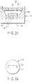
- FIG. 1A is a partial cross-sectional side view schematically showing an example of a light-emitting device (no embodiment of the invention).
- This light-emitting device includes, as main constituent elements, a support body (radiation plate) 11 provided with lead terminals 10, a light-emitting element (an LD chip in this example) 12 mounted on the support body, a translucent covering member 13 covering (sealing) the light-emitting element, a cylindrical reflector 14 which is constituted by, for example, a metallic body, placed to surround the light-emitting element and fixed to the support body, and a cap 15 which is placed to cover an opening part of the reflector and is held at an opening distal end part of the reflector.
- the light-emitting element 12 is mounted on the support body at, for example, a central part thereof, in such a state that the element 12 emits an output emission light in a direction of the opening distal end of the reflector.
- a light reflection surface 14a inclined toward the distal end of the reflector at a peripheral part of the light-emitting element is formed.
- the above-mentioned cap 15 includes, for example, a solid fluorescent member 16 containing a fluorescent substance in at least a part thereof as a wavelength conversion member which is excited by light from the light-emitting element 12, and emits light having a wavelength different in emitting color from the light emitted by the light-emitting device.
- an outer circumferential surface of the disk-like fluorescent member 16 is held by a translucent member 17 as shown in FIG. 1B .
- the output emitted light of the light-emitting element 12 is made directly incident on the fluorescent member 16 at the central part of the cap, and light emitted by the fluorescent substance excited by the incident light is output to the outside in front of the reflector.
- the light emitted by the fluorescent substance may be color-mixed with the output emitted light of the light-emitting element 12. It becomes possible for the light emitted by the fluorescent member 16 in the direction of the support body to pass through the translucent member 17 around the fluorescent member and to be efficiently output to the front of the reflector after being reflected by the light reflection surface 14a and a top surface of the support body, thereby improving the outcoupling efficiency of light.
- a diffusion material for diffusing the emitted output light of the light-emitting element 12 may be mixed in the fluorescent member 16. Thus, the directivity can be improved.
- the directivity of the emitted output light of the light-emitting element 12 is high and thus the area of the fluorescent member 16 to be excited by the light from the light-emitting element 12 can be made small. Consequently, a ratio of the intensity of light to the light emission area becomes larger, and a higher luminance can be achieved. Further, the outer circumference of the fluorescent member 16 is firmly held by the translucent member 17, and hence even when the fluorescent member 16 is irradiated with high-energy light, the fluorescent member does not come off.
- the entire emitted output light of the light-emitting element 12 is uniformly wavelength-converted, and hence there is no possibility of color irregularity being caused at the fluorescent member 16.
- the light-emitting element 12 is a chip of a surface-emitting LED, only a part of the emitted output light illuminates the fluorescent member 16 to be wavelength-converted, and hence there is the possibility of color irregularity being caused between the irradiated part and a peripheral part thereof.
- the plane shape of the fluorescent member 16 is not limited to the circular shape shown in FIG. 1B , and is made to have a shape corresponding to the cross sectional beam pattern shape (for example, an elliptic shape) of the emitted output light from the light-emitting element on the irradiated surface, whereby it becomes possible to make the fluorescent substance emit light efficiently and to obtain output light with high intensity.
- the plane shape of the fluorescent member 16 may be made to completely coincide with the cross sectional beam pattern shape of the emitted output light from the light-emitting element 12 on the irradiated surface.
- the plane shape of the fluorescent member 16 may also be set larger or smaller than the pattern shape of the beam cross section.
- the fluorescent member 16 may have a difference in the wavelength conversion capability in the plane.
- the amount of the fluorescent substance may be distributed in such a state that the amount of the fluorescent substance is denser at the central part of the pattern shape of the beam cross section than at the peripheral part thereof.
- the support body 11 is made of a metallic material or an insulating substrate excellent in thermal conductivity with a plurality of lead terminals 10 attached thereto. It is desirable that a film of high reflectance (not shown) be formed on the surface of the support body.
- the number of light-emitting elements mounted and installed on the support body is arbitrary, and may be one or more.
- a pair of electrodes of the light-emitting element is electrically connected each to a single lead terminal of the support body.
- one of the electrode surfaces of the light-emitting element is connected to one lead terminal by die bonding, and the other electrode surface of the light-emitting element is connected to another lead terminal through a conductive wire.
- the output structure of the light-emitting element is arbitrary and may be, for example, of a surface-emitting, of an edge-emitting, or of a ridge array.
- a light-emitting element for emitting blue light having an emission peak wavelength in the vicinity of 460 nm, a light-emitting element for emitting bluish purple light having an emission peak wavelength in the vicinity of 410 nm, a light-emitting element for emitting ultraviolet light having an emission peak wavelength in the vicinity of 365 nm, and the like can be used.
- the type of the light-emitting element is not particularly limited. However, for example, a light-emitting element having a structure obtained by forming a nitride semiconductor such as InN, AlN, GaN, InGaN, AlGaN, InGaAlN, and the like as a light-emitting layer on a substrate by MOCVD method or the like is used. For example, a light-emitting element having a structure formed by stacking an n-type contact layer made of n-type GaN, an n-type cladding layer made of n-type AlGaN, and a p-type contact layer made of p-type GaN one on top of another in this order on a sapphire substrate is used.
- the emission wavelength of the light-emitting element can be variously selected according to the material of the semiconductor and the mixed crystal ratio thereof. For example, by changing the InGaN content or type of impurities with which the active layer is doped, it is possible to change the emission wavelength from the ultraviolet region to the red region.
- the covering member 13 High transparency for light is required to the covering member in order to allow the light from the light-emitting element to efficiently pass therethrough.
- the covering member also serves to protect the conductive wire.
- translucent resin excellent in weather resistance such as epoxy resin, silicone resin, acrylic resin, urea resin, and the like or glass excellent in light resistance is suitably used.
- the translucent resin contains a diffusing agent such as silicon dioxide or aluminum oxide, it is also possible to lower the directivity of light from the light-emitting element and to make the view angle wider.
- the material of the reflector is not particularly limited, and the light reflection surface 14a can be formed into an arbitrary shape, such as a gradual curve, cup-like shape, or tapered shape.
- the cap includes in at least a part thereof a solid fluorescent member 16 containing a fluorescent substance which is excited by light from the light-emitting element and emits light having a color different from the color of the light emitted by the light-emitting element.
- An example of the cap includes a circular opening at, for example, a central part of a circular ring-like translucent member (for example, translucent member) as shown in FIG. 1B , and the solid fluorescent member 16 containing a fluorescent substance is present at the central opening.
- Solid fluorescent member 16 An example of the solid fluorescent member is that formed by binding a fluorescent substance using a binder such as glass, which is an inorganic material, and hardening the bound fluorescent substance.
- fluorescent glass formed by binding the fluorescent substance with glass is used.
- a fluorescent substance is arranged on a bottom surface of a cap-forming container at, for example, a central part thereof, and after filling the peripheral part with molten glass, the resultant is hardened.
- the fluorescent substance absorbs light from the light-emitting element, and converts the light into light having a different wavelength, and a YAG fluorescent substance, a nitride fluorescent substance, and other fluorescent substances can be used as the fluorescent substance.
- the fluorescent substance is at least one substance selected from, for example, a nitride-based fluorescent substance/oxynitride-based fluorescent substance mainly activated with lanthanoid such as Eu and Ce; an alkaline-earth halogen apatite fluorescent substance, alkaline-earth metal boric acid halogen fluorescent substance, alkaline-earth metal aluminate fluorescent substance, an alkaline-earth silicate, alkaline-earth sulfide, alkaline-earth thiogallate, alkaline-earth silicon nitride, and germanate mainly activated with lanthanoid such as Eu or transition metal such as Mn; a rare-earth aluminate and rare-earth silicate mainly activated with lanthanoid such as Ce; and organic and inorganic complexes mainly activated with lanthanoid such as Eu.
- fluorescent substances fluorescent substances exhibiting emission spectra corresponding to yellow, red, green, and blue when excited by the light from the light-emitting element can be used.
- fluorescent substances having spectra corresponding to neutral colors of these colors e.g., yellow, bluish green, orange, and the like can also be used.
- light-emitting devices having various luminescent colors can be manufactured.
- a GaN-based compound semiconductor which emits blue light when, for example, a GaN-based compound semiconductor which emits blue light is used as a light-emitting element, Y 3 Al 5 O 12 :Ce or (Y 0.8 Gd 0.2 ) 3 Al 5 O 12 :Ce is used as a fluorescent substance, and wavelength conversion is performed by irradiating a YAG fluorescent substance with light from the light-emitting element, it is possible to provide a light-emitting device which emits whitish mixed color obtained by mixing the light from the light-emitting element and light from the fluorescent substance.
- the translucent member is made of, for example, translucent member, regardless of whether or not an HR coat or an AR coat for protection against light emitted by the LD chip is present.
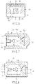
- FIG. 7 is a partial cross-sectional side view schematically showing another example of a light-emitting device (no embodiment of the invention).
- This light-emitting device includes, as main constituent elements, a support body 11 provided with lead terminals 10, a light-emitting element (an LD chip in this example) 12 mounted on the support body at a central part thereof, a translucent covering member 13 covering (sealing) the light-emitting element, a receptacle 71, a convergent lens 72, and a solid fluorescent member 73 containing a fluorescent substance and having a convex lens-like shape.
- the receptacle 71 is constituted by, for example, a cylindrical metallic body, has a proximal side fixed to the periphery of the support body 11, is placed to surround the circumference of the light-emitting element 12, and has a cup section 71a, for example, integral therewith and protruding from an intermediate part of the inner surface.
- a light-transmitting opening (aperture) 71b is formed at the central part thereof, and a light reflection surface 71c having, for example, a hemispherical (or tapered) shape opened on the side of the distal end of the receptacle is formed.
- the fluorescent member 73 is placed to cover the distal end face of the cup section 71a on the side of the opening. Further, the convergent lens 72 is placed within the space in the receptacle at a position closer to the light-emitting element side than the cup section 71a and allows light from the light-emitting element to converge and the light to pass through the aperture 71b so as to make the light incident on the fluorescent member 73.
- the support body 11 and the light-emitting element 12 are the same as those previously described in the first example, and the solid fluorescent member 73 is, for example, fluorescent glass.
- the light reflection surface 71c of the cup section 71a of the receptacle can be formed into an arbitrary shape, such as a gradual curve, cup-like shape, and tapered shape.
- a ratio of a light component (return light) which returns to the light-emitting element side through the small aperture 71b with respect to the total light emitted by the excited fluorescent substance becomes very small, and most of the light emitted by the fluorescent substance is directly output to the front of the receptacle or is reflected by the light reflection surface 71c to be output to the front of the receptacle, thereby achieving high-luminance output emission.
- the load on the fluorescent substance is lowered, the saturation intensity of the excitation light that induces emission is increased, and the luminous efficiency and linearity are improved.
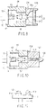
- FIG. 9 is a side view schematically showing an example of a light-emitting device of a solid fluorescent member mounting type according to another example (no embodiment of the invention).
- This light-emitting device includes, as main constituent elements, a support body 11 provided with lead terminals 10, a light-emitting element (an LD chip in this example) 12 mounted on the support body at a central part thereof, a translucent covering member 13 covering (sealing) the light-emitting element, a receptacle 91, a cup 91a formed separately from the receptacle, a convergent lens 92, and a cap 95 provided with a solid fluorescent member 93 at a central part thereof.
- the receptacle 91 is constituted by, for example, a cylindrical metallic body, a distal end part thereof is formed thick, and the cup 91a is fixed (for example, welded) to an end face surrounding an opening of the receptacle 91 in such a state that the cup 91a faces and is in contact with the end face.
- the distal end part of the light reflection surface 91c is provided with a step section 91b at a position near the intermediate part of the cup 91a.
- the cap 95 is fixed to a bottom surface of the step section 91b, and is placed to cover the opening part (inside the distal end at the opening of the receptacle) of the cup 91a.
- the circumferential surface of the disk-like fluorescent member 93 is held by a translucent member 94.
- the cup section 91a can be fixed in the state that an alignment desired for making the light from the convergent lens 92 incident on the small fluorescent member 93 has been achieved. Further, the open distal end part of the receptacle that protrudes from the step section 91b of the cup section 91a serves to increase the directivity of the output light.
- FIG. 10 is a side view schematically showing an example of a light-emitting device of a solid fluorescent member mounting type according to another example (no embodiment of the invention).
- the light-emitting device shown in FIG. 10 differs from the light-emitting device of FIG. 9 described previously in the respect that a light guide 100 formed separately from a receptacle 91 is fixed to an end face of a receptacle surrounding an opening thereof instead of the cup 91a and the cap 95.
- This light guide 100 includes a ferrule 101 made of metal and provided with a thin optical fiber insertion hole at a central part thereof and a flexible light guide member (for example, an optical fiber 102) inserted into the central part of the ferrule.
- a small solid fluorescent member 103 is held at or attached to an end face of the optical fiber 102, and the ferrule is fixed in the state that a proximal end face thereof faces and is in contact with the distal end face of the receptacle surrounding the opening thereof.
- the light guide 100 can be fixed in the state that an alignment desired for making the converging light incident on one end face of the optical fiber 102 has been achieved.
- the light incident on the end face of the optical fiber 102 is further made incident on the fluorescent member 103 at the end face part of the optical fiber through the optical fiber 102, and hence high-luminance output emission can be obtained.
- replacement of the light guide 100, ferrule 101, optical fiber 102, and fluorescent member 103 can be made easily, and a mounting yield is also improved.
- the ferrule 101 may be omitted, and the light guide member may be held such that the proximal end face of the light guide member faces and is in contact with the distal end face of the receptacle surrounding the opening thereof.
- FIG. 11 is a side view schematically showing an example of a solid fluorescent member-mounting type light-emitting device according to another example (no embodiment of the invention).
- the light-emitting device shown in FIG. 11 includes, as main constituent elements, a support body 11 provided with lead terminals 10, a sub-mount 11a placed on the support body, a light-emitting element (an LD chip in this example) 12 mounted on the sub-mount, and a solid fluorescent member (for example, fluorescent glass) 113 placed on the support body 11 and having a hemispherical cross section (lamp-shaped, shell-shaped).
- the light-emitting element 12 is mounted in the state that output light is emitted sideways, and the fluorescent glass 113 is placed to face the light-emitting element 12.
- the light from the light-emitting element 12 is made directly incident on the fluorescent member 113 to excite the fluorescent substance, and the light emitted by the fluorescent substance and the light from the light-emitting element 12 are output to the upward position of the support body 11.
- the number of members used is small, and the number of steps necessary for assembly is also small, and hence high-luminance output emission can be obtained while the manufacturing cost can be reduced.
- the light-emitting element 12 and the fluorescent member 113 are directly arranged on the support body 11, whereby it becomes possible to efficiently radiate heat generated from the light-emitting element 12 and the fluorescent member 113, and the thermal resistance of the heat radiation path is reduced. As a result of this, the load on the light-emitting element 12 and the fluorescent member 113 is decreased, thus improving the luminous efficiency and linearity. Further, the light emitted by the light-emitting element 12 has directivity, and hence it becomes possible to efficiently irradiate the small fluorescent member 113 with light, thereby improving the luminance.
- FIG. 1A schematically shows the structure of a light-emitting device of Example 1.
- This light-emitting device is a specific example of the first example described previously, and includes a support body 11 provided with lead terminals 10, an LD chip 12, translucent resin 13, a cylindrical reflector 14 constituted by, for example, a metallic body, and a cap 15.
- the LD chip 12 is mounted on the support body at, for example, a central part thereof such that it emits output light in the direction of the distal end of the reflector on the side of the opening.
- the cap 15 is provided with a circular opening at a central part of a translucent member plate 17 having a circular ring-like shape, and a solid fluorescent glass 16 is present in the opening at the center.
- a proximal end part of the reflector 14 is fixed to periphery of the support body 11, and periphery of the cap 15 is fixed to a bottom surface of a step section 14b formed on the inside of the distal end part of the reflector.
- the output light emitted by the LD chip 12 is made directly incident on the fluorescent glass 16 at the central part of the cap, and the light emitted by the fluorescent substance excited by the incident light is output to the front of the reflector.
- the area of the fluorescent glass 16 is small, and hence realization of high luminance is enabled.
- FIG. 2A schematically shows the structure of a light-emitting device of Example 2.
- This light-emitting device differs from the light-emitting device previously described with reference to FIG. 1A in the respect that the device includes an LD array in which a plurality of (for example, two) LD chips 12 are arranged and mounted, and a cap 25 is provided with a rectangular opening at a central part thereof as shown in FIG. 2B , and a fluorescent glass 26 is present at the rectangular opening.
- the same effect as that previously described for the light-emitting device with reference to FIGS. 1A and 1B can be obtained. Furthermore, when the fluorescent glass 26 of the cap 25 is provided in accordance with an emergence pattern of the light from the LD chip 12, it becomes possible to make the fluorescent substance efficiently emit light and to obtain high-luminance output light.
- the LD array has a characteristic of emitting light in an irradiation pattern in which the light beam is more expanded in the vertical direction than in the horizontal direction, it is possible to form the fluorescent glass 26 into an elliptic shape in accordance with the characteristic.
- the opening of the cap 25 may be a thin and long opening.
- a plurality of short rectangular openings may be formed in an array in accordance with irradiation patterns of light beams from the LD chips 12, and a fluorescent glass 26 may be arranged at each of the openings.
- FIG. 3 schematically shows the structure of a light-emitting device of Example 3.
- This light-emitting device differs from the light-emitting device previously described with reference to FIG. 1A in the respect that a light reflection surface of a reflector 34 is, for example, hemispherical, and that a convergent lens 33 for making light from an LD chip 12 convergent and the converging light incident on a fluorescent glass 16 (the lens has a focal point at a position of the fluorescent glass 16) is placed within the space surrounded by the reflector 34.
- the same effect as that previously described for the light-emitting device with reference to FIGS. 1A and 1B can be obtained, and further, it is possible to make the light from the LD chip 12 convergent by means of the convergent lens 33 and make the converging light incident on the fluorescent glass 16. This makes it possible to make the fluorescent glass 16 small and enhance the intensity of light for exciting the fluorescent substance, thereby improving the luminance.
- FIG. 4 schematically shows the structure of a light-emitting device of Example 4.
- This light-emitting device differs from the light-emitting device previously described with reference to FIG. 1A in the respect that a solid fluorescent glass 46 constituted only by a fluorescent member and having a disk-like shape is used instead of the cap 15, and that an LD chip 12 is sealed with low-melting glass 47 inside the reflector 14. It is possible that the low-melting glass 47 is not be used and the inside of the reflector 14 is filled with an inorganic binder or inert gas such as N 2 and Ar.
- an inorganic binder or inert gas such as N 2 and Ar.
- the output light emitted by the LD chip 12 is made directly incident on the fluorescent glass 46, and the light emitted by the excited fluorescent substance is output to the outside (the front of the reflector). At this time, the light emitted by the fluorescent substance may be color-mixed with the output light emitted by the LD chip 12. Further, since the fluorescent glass 46 is placed to cover the entire surface of the reflector opening and the light from the LD chip 12 is made incident on the entire surface of the fluorescent substance, the load on the fluorescent substance is lowered and the luminous efficiency and linearity are improved.
- the inside of the reflector 14 is sealed with low-melting glass 47, and hence the refractive index of the fluorescent glass 46 and the refractive index inside the reflector can be matched with each other. As a result of this, it becomes possible to efficiently guide the light from the LD chip 12 to the fluorescent glass 46, which improves the luminance.
- the LD chip 12 is sealed with low-melting glass 47 inside the reflector, and hence it is possible to protect the LD chip 12 from external impact, moisture, and the like.
- the fluorescent glass 46 is placed to cover the entire surface of the opening of the reflector 14, and the light from the LD chip 12 can be made incident on the entire surface of the fluorescent substance, and hence it becomes possible to obtain higher-luminance output light.
- the fluorescent glass 46 is made to be thicker than the peak wavelength (for example, 445 nm) of the output light emitted by the LD chip 12, and hence it is possible for the fluorescent substance to be excited by the light from the LD chip 12 and emit light.
- the thickness of the fluorescent glass 46 is set at about 100 ⁇ m to 500 ⁇ m, a degree of light diffusion is improved, and color irregularity of the emitted output light is reduced.
- FIG. 5 schematically shows the structure of a light-emitting device of Example 5.
- This light-emitting device differs from the light-emitting device previously described with reference to FIG. 4 in the following respects. Sealing using the low-melting glass 47 is not performed. Further, a periphery of a highly thermal conductive member 51 having a plate-like shape is fixed to and held on a bottom surface (distal end face of reflector) of a step section of a reflector 14 so as to cover a distal end face of the reflector 14 surrounding an opening thereof. Further, a disk-like fluorescent glass 46 is laid on the front side of the member 51 so as to be fixed thereto. The arrangement order of the highly thermal conductive member 51 and the fluorescent glass 46 may be reversed.
- the highly thermal conductive member 51 is placed to cover the opening part of the reflector.
- the inside of the reflector is sealed with a double cap structure constituted by the highly thermal conductive member 51 and the fluorescent glass 46, and hence the LD chip 12 is not adversely affected by moisture and the like. Further, it becomes possible to efficiently radiate heat generated from the fluorescent glass 46 by the highly thermal conductive member 51, and hence the load on the fluorescent glass 46 is lowered, and the luminous efficiency and linearity are improved.
- FIG. 6 schematically shows the structure of a light-emitting device of Example 6.
- This light-emitting device differs from the light-emitting device of FIG. 5 described previously in the respect that a functional filter 61 is placed on the undersurface side of a fluorescent glass 46 and between the fluorescent glass 46 and a highly thermal conductive member 51.
- This functional filter 61 is constituted by a multilayer film of dielectric substances having a high reflectance characteristic with respect to light (light having a wavelength longer than that of the excitation light emitted by an LD chip 12) other than the light from the LD chip 12.
- An example of the specific material is a material containing at least one selected from SiO 2 , ZrO 2 , Al 2 O 3 , AlN, ZnO, TiO 2 , SiN, Ta 3 O 5 , MgF 2 , Si 3 N 4 , MgO, HfO 2 , and Nb 2 O 5 .
- the functional filter 61 arranged to cover the opening section of the reflector makes it possible to reflect light returning from the fluorescent glass 46 to the LD chip side and efficiently output light to the front of the reflector.
- the functional filter 61 is placed on the top surface side (front side of the reflector) of the fluorescent glass 46, it becomes possible to reflect any excitation light that was not used to excite the fluorescent substance back towards the fluorescent glass 46 side, thereby improving the outcoupling efficiency of the light.
- FIG. 7 schematically shows the structure of a light-emitting device of Example 7, which is a specific example of the second embodiment described previously.
- This light-emitting device includes a support body 11 provided with lead terminals 10, an LD chip 12 mounted on the support body at a central part thereof, a translucent covering member 13 covering (sealing) the LD chip, a cylindrical receptacle 71 constituted by a metallic body, a convergent lens 72, and a fluorescent glass 73.
- the receptacle 71 is fixed at, for example, the proximal end side thereof to the periphery of the support body 11, and is placed to surround the LD chip 12.
- a cup section 71a integral therewith and protruding from an intermediate part of the inner surface is formed.
- an aperture 71b is formed at the central part thereof, and a light reflection surface 71c having, for example, a hemispherical (or tapered) shape open at the distal end of the receptacle is formed.
- an inner surface of the distal end part of the receptacle and a distal end surface of the cup section form a step section.
- the fluorescent glass 73 having, for example, a convex lens-like shape is placed to cover the surface of the distal end of the cup section 71a surrounding the opening thereof.
- the periphery of the fluorescent glass 73 is fixed to the distal end face (bottom surface of the step section) of the cup section so as to be held.
- the convergent lens 72 is placed within the space inside the receptacle closer to the LD chip side than the cup section 71a. The convergent lens 72 allows the light from the LD chip 12 to converge and the converging light to pass through the aperture 71b so as to make the light incident on the fluorescent glass 73.
- the support body 11 and the LD chip 12 are the same as those previously described in Example 1.
- the light reflection surface 71c of the cup section 71a of the receptacle 71 can be formed into an arbitrary shape, such as a gradual curve, cup-like shape, or tapered shape.
- a ratio of return light (light which passes through the small aperture to return to the LD chip side) with respect to the total light emitted by the excited fluorescent substance becomes very small, and most of the light is directly output to the front of the receptacle or is reflected by the light reflection surface 71c to be output to the front of the receptacle.
- the fluorescent glass 73 in a large size as a cap covering the distal end face of the cup section 71a surrounding the opening such that the front surface of the fluorescent glass 73 having the lens (for example, a convex lens)-like shape protrudes from the distal end of the receptacle.
- the load on the fluorescent substance is lowered, the saturation intensity of the excitation light that induces emission is increased, and the luminous efficiency and linearity are improved.
- FIG. 8 schematically shows the structure of a light-emitting device of Example 8.
- a cap 15 similar to that described in the first embodiment is used in stead of the convex lens-like fluorescent glass 73 of the light-emitting device previously described with reference to FIG. 7 .
- a fluorescent glass 16 is placed at a central part of a disk-like translucent member (for example, a translucent member plate 17) as shown in, for example, FIG. 1B .
- the fluorescent glass 16 by positioning the fluorescent glass 16 in the vicinity of the focal point of a convergent lens 72, it is possible to make the light from the convergent lens 72 incident on the fluorescent glass 16, excite the fluorescent substance, and make the fluorescent substance emit output light to the front of the receptacle.
- the area of the fluorescent glass 16 is small, and hence high luminance can be realized.
- the light emitted by the fluorescent glass 16 to the inside of the cup section 71a to pass through the translucent member plate 17 around the fluorescent glass and efficiently output to the front of the receptacle after being reflected by a light reflection surface 71c of the cup section 71a, thereby improving the outcoupling efficiency of the light.
- FIG. 9 schematically shows the structure of a light-emitting device of Example 9 which is a specific example of the third embodiment described previously.
- This light-emitting device differs from the light-emitting device previously described with reference to FIG. 8 in the respect that a distal end part of a receptacle main body 91 is formed thick, a cup 91a is formed separately from the receptacle main body 91, and the cup 91a is fixed (for example, by welding) to an end face of the receptacle main body 91 surrounding an opening thereof in such a state that the cup 91a faces and is in contact with the end face.
- a step section 91b is formed at a position near the intermediate part of the cup 91a and at the distal end part of the light reflection surface 91c. Further, a cap 95 is fixed to a bottom surface of the step section 91b, and is placed to cover the opening part (inside the distal end at the opening of the receptacle) of the cup 91a.
- the open distal end part of the receptacle that protrudes from the step section of the cup section 91a serves to increase the directivity of the output light.
- FIG. 10 schematically shows the structure of a light-emitting device of Example 10, which is a specific example of the fourth embodiment described previously.
- This light-emitting device differs from the light-emitting device previously described with reference to FIG. 9 in the respect that a light guide 100 formed separately from a receptacle (holding member) 91 is fixed to a periphery of a receptacle surrounding an opening thereof in stead of the cup 91a and the cap 95.
- This light guide 100 includes a ferrule 101 made of metal, and a light guide member (an optical fiber 102 in this example).
- a small fluorescent glass 103 is held at an end face of the optical fiber 102 in the state that the fluorescent glass 103 is pressed against the optical fiber end face side by, for example, a spring (not shown).
- the ferrule 101 is provided with a thin optical fiber insertion hole at a central part thereof, and the optical fiber 102 is inserted into the central part of the ferrule. Further, the ferrule is fixed in the state that a proximal end face of the ferrule faces and is in contact with the distal end face of the receptacle surrounding the opening thereof.
- the light guide 100 can be fixed in the state that alignment with respect to the receptacle 91 has been achieved such that the light, which the convergent lens 92 has made converge, incident on one end face of the optical fiber 102.
- the light incident on the end face of the optical fiber 102 is further made incident on the fluorescent glass 103 at the end face part of the optical fiber through the optical fiber 102, and hence high-luminance output emission can be obtained.
- replacement of the light guide 100, ferrule 101, optical fiber 102, and fluorescent glass 103 can be made easily, and a mounting yield is also improved.
- the optical fiber 102 is thin, the amount of return light from the fluorescent glass 103 on the distal end face side to the LD chip side is small.
- FIG. 11 schematically shows the structure of a light-emitting device of Example 11, which is a specific example of the fifth embodiment described previously.
- This light-emitting device includes a support body 11 provided with lead terminals 10, a sub-mount 11a placed on the support body, an LD chip 12 mounted on the sub-mount in the state that output light is emitted sideways, and a fluorescent glass 113 placed on the support body 11 to face the LD chip 12 and having a hemispherical cross section (lamp-shaped, shell-shaped).
- the light from the LD chip 12 is made directly incident on the fluorescent glass 113 to excite the fluorescent substance, and the light emitted by the fluorescent substance and the light from the LD chip 12 are output upwardly above the support body 11.
- the number of members used is small, and the number of steps necessary for assembly is also small, and hence high-luminance output emission can be obtained while the manufacturing cost can be reduced.
- the LD chip 12 and the fluorescent glass 113 can be directly arranged on the support body 11, whereby it becomes possible to efficiently radiate heat generated from the LD chip 12 and the fluorescent glass 113, and the thermal resistance of the heat radiation path is reduced. As a result of this, the load on the LD chip 12 and the fluorescent glass 113 is lowered, and the luminous efficiency and linearity are improved. Further, the light emitted by the LD chip 12 has directivity, and hence it becomes possible to efficiently irradiate the small fluorescent glass 113 with light, thereby improving the luminance.
- FIG. 12 schematically shows the structure of a light-emitting device of Example 12.
- This light-emitting device differs from the light-emitting device of FIG. 11 described previously in the respect that a flat plate-like fluorescent glass 123 is placed on a support body 11, and an LD chip 12 is mounted on the fluorescent glass 123 in the state that output light of the LD chip is emitted in the downward direction.
- the light from the LD chip 12 is made directly incident on the fluorescent glass 123 below the LD chip 12 so as to excite the fluorescent substance, and the light emitted by the fluorescent substance is output upwardly above the support body.
- the same effect as that previously described for the light-emitting device with reference to FIG. 11 can be obtained.
- FIG. 13 schematically shows the structure of a light-emitting device of an embodiment of the invention.
- This light-emitting device differs from the light-emitting device of FIG. 12 described previously in the respect that an LD chip 12 is directed obliquely downward on a holding pedestal 131 mounted on the support body 11, and light from the LD chip 12 is made directly incident on a fluorescent glass 133 obliquely below the LD chip 12.
- the same effect as that previously described for the light-emitting device with reference to FIG. 11 can be obtained. Further, the light emitted by the fluorescent substance of the fluorescent glass 133 is output in the upward and lateral directions above the support body without being intercepted by the LD chip 12 obliquely above the glass body 133 and the holding pedestal 131, and hence the outcoupling efficiency of the light is improved.
- FIG. 14 schematically shows the structure of a light-emitting device of Example 13.
- a double edge-emitting LD chip 143 is used.
- output light can be obtained from both edges in an arbitrary ratio by controlling the reflectance of each of the mirrors on both edges of the chip.
- the LD chip 142 is mounted on a support body 11 provided with lead terminals 10 in the state that both emission edges faces the right and left sides, and two fluorescent glass 143 having a dome-like (lamp-like, shell-like) shape are arranged on both sides of the LD chip 142 so as to face the LD chip.
- the fluorescent glass 143 can be formed into an arbitrary shape such as a dome-like shape, and a square pillar-like shape. As a result of this, it is possible to make the light from the LD chip 142 directly incident on each of the fluorescent glass 143 on both sides and excite each of the fluorescent glass 143 so as to make each of them emit light.
- the same effect as that previously described for the light-emitting device with reference to FIG. 11 can be obtained. Moreover, the load on the fluorescent substance is lowered, and the luminous efficiency and linearity are improved. Incidentally, by using fluorescent substances different from each other in the two fluorescent glass 143, it is possible to make the fluorescent glass 143 emit light components having wavelengths different from each other without causing the interference of the light components emitted by the two fluorescent glass.
- FIG. 15 schematically shows the structure of a light-emitting device of Example 14.
- an LD chip 12 is mounted on a support body 11 provided with lead terminals 10 such that the LD chip 12 emits output light upwardly above the support body, and flat plate-like fluorescent glass 153 are arranged on both sides or around the LD chip 12.
- a cylindrical reflector 151 is fixed on the support body 11 so as to cover the LD chip 12 and the fluorescent glass 153, and, as a cap for closing the distal end opening of the reflector 151, for example, a glass plate 152 is held thereon.
- a reflection film (not shown) for reflecting light from the LD chip 12 is formed on a part of the inner surface or the entire inner surface of the glass plate 152.
- the light from the LD chip 12 is reflected by the inner surface of the glass plate 152 above the LD chip 12, and the reflected light is made incident on the fluorescent glass 153 to excite the fluorescent substance.
- Light emitted by the fluorescent substance passes through the glass plate 152 and is output upwardly above the support body directly or after being reflected by the inner surface of the reflector 151.
- FIG. 16 schematically shows the structure of a light-emitting device of Example 15.
- an LD chip 12 is mounted on a support body 11 provided with lead terminals 10 such that the LD chip 12 emits output light upwardly above the support body, and a dome-like fluorescent glass 163 is arranged to cover the LD chip 12.
- the light from the LD chip 12 is made incident on the fluorescent glass 163 to excite the fluorescent substance, and the light emitted by the fluorescent substance passes through the fluorescent glass 163 to be output to the outside of the dome directly or after being reflected by the surface of the support body.
- a semiconductor light-emitting device wherein in a semiconductor light-emitting device, light from a laser diode is output to the outside after the luminance of the light being enhanced. It includes a support body 11 provided with lead terminals 10, one or more laser diodes 12 mounted on the support body, a cylindrical reflector 14 fixed to the support body to surround the laser diode(s) and provided with a light reflection surface formed on an inner surface thereof, and a cap 15 placed to cover an opening distal end face of the reflector and held at an opening distal end part of the reflector 14, the cap 15 being provided at a central part thereof with a solid fluorescent member 16 including a fluorescent substance that is excited by the light from the laser diode 12 and emits light different in colors from light emitted by the laser diode 12.
- a light-emitting device comprising a support body; a light-emitting element constituted by a laser diode mounted on the support body; a cylindrical reflector fixed to the support body and provided with a light reflection surface on its inner surface surrounding the light-emitting element; and a cap provided at a part thereof with a wavelength conversion member, the wavelength conversion member emitting light having a wavelength different from that of the light emitted by the light-emitting element when irradiated with light from the light-emitting element, and the cap being placed on the reflector to cover an opening part of the reflector.
- a planar shape of the wavelength conversion member is a shape in which a cross-sectional beam pattern shape of emitted output light from the light-emitting element on an irradiated surface is mostly included.
- the wavelength conversion member is positioned at a central part of the cap and a planar shape of the wavelength conversion member is substantially coincident with a cross-sectional beam pattern shape of emitted output light from the light-emitting element on an irradiated surface.
- a cross-sectional beam pattern shape of emitted output light from the light-emitting element on an irradiated surface is an ellipse and a planar shape of the wavelength conversion member includes a major axis of the ellipse.
- the wavelength conversion member is held by a translucent member at an outer circumference thereof.
- the light-emitting device further may comprise a convergent lens placed inside the reflector to make light from the light-emitting element converge and the converging light incident on the wavelength conversion member; and/or a sealing member for sealing the light-emitting element inside the reflector.
- a thermal conductive member is provided such that it covers the wavelength conversion member at an opening part of the reflector.
- a dielectric film for reflecting light having a wavelength longer than a wavelength of light from the light-emitting element and the wavelength conversion member can be arranged in the order mentioned from the light-emitting element side such that they cover an opening part of the reflector.
- the wavelength conversion member further includes a diffusion material for diffusing emitted light from the light-emitting element.
- a light-emitting device comprising a support body a light-emitting element constituted by a laser diode mounted on the support body; a cylindrical receptacle fixed to the support body in such a manner that an inner surface thereof surrounds the light-emitting element; a cup section including a light reflection surface inclined from a light-transmitting aperture, which is produced by partially protruding an inner surface of the receptacle, toward a distal end of an opening part of the receptacle; a cap including a wavelength conversion member in at least a part thereof and provided such that it covers an opening part of the cup section; and a convergent lens placed in the receptacle at a position closer to the light-emitting element side than the cup section and allowing light from the light-emitting element to converge and the converging light to pass through the aperture, thereby making the light incident on the wavelength conversion member.
- the cap is constituted by a lens-like wavelength conversion member; and/or the wavelength conversion member is held by a translucent member at an outer circumference thereof.
- a light-emitting device comprising a support body; a light-emitting element constituted by a laser diode mounted on the support body; a cylindrical receptacle fixed to the support body in such a manner that an inner surface thereof surrounds the light-emitting element; a cup fixed to a distal end part of the receptacle at a proximal end part thereof and including a light reflection surface inclined from a light-transmitting aperture, which is produced by protruding a part of an inner surface thereof, toward a distal end of an opening part thereof; a cap including a wavelength conversion member in at least a part thereof and placed such that it covers an opening part of the cup; and a convergent lens placed in the receptacle at a position closer to the light-emitting element side than the cup section and allowing light from the light-emitting element to converge and the converging light to pass through the
- the wavelength conversion member is held by a translucent member at an outer circumference thereof.
- a light-emitting device comprising a support body; a light-emitting element constituted by a laser diode mounted on the support body; a cylindrical receptacle fixed to the support body in such a manner that an inner surface thereof surrounds the light-emitting element; a light guide member a proximal end face of which faces and is in contact with an end face of the receptacle surrounding an opening thereof; a wavelength conversion member fixed to a distal end face of the light guide member; and a convergent lens placed in the receptacle at a position closer to the light-emitting element side than the light guide member and making light from the light-emitting element converge and the converging light incident on one end side of the light guide member.
- a holding member provided with a light guide member insertion hole into which the light guide member is inserted, and fixed such that a proximal end face thereof faces and is in contact with a face of the receptacle surrounding an opening thereof.
- a light-emitting device comprising: a support body; a light-emitting element emitting light from a laser diode chip and being mounted on the support body; and a wavelength conversion member mounted on the support body where it receives a peak intensity of irradiation by the light-emitting element and emitting light different in wavelengths from light emitted by the light-emitting element when the light-emitting element emits the light.
- the light-emitting device of the present invention can be applied to a light source for illumination, a light source for various indicators, an onboard light source, a light source for a display, a light source for a backlight of a liquid crystal display, and the like.
Description
- The present invention relates to a light-emitting device, and more particularly, to a structural arrangement of a wavelength conversion member in a light-emitting device in which a chip of a laser diode is used as a light-emitting element.
- A light-emitting device in which a chip of a laser diode (LD) or a light-emitting diode (LED) is used as a light-emitting element is small in size, is of low power consumption, and has a long service life. Hence, such a light-emitting device is used in a wide range of the fields, e.g., backlight of a liquid crystal display, onboard use, and the like. Light emitted by such light-emitting elements is monochromatic light of limited colors such as red, green, and blue. Such light-emitting elements are sometimes used in combination with a fluorescent substance for converting the monochromatic light into light of a different wavelength. For example, a light-emitting device is known in which light from a light-emitting element directly output to the outside, light emitted by the light-emitting element, and wavelength-converted light emitted by a fluorescent substance are color-mixed with one another, thereby emitting white-colored light.
- Incidentally, in Jpn. Pat. Appln. KOKAI Publication No.
11-87784 - Further, in Jpn. Pat. Appln. KOKAI Publication No.
2003-258308 - Further, in Jpn. Pat. Appln. KOKAI Publication No.
2005-20010 - On the other hand, in Jpn. Pat. Appln. KOKAI Publication No.
2003-295319 - Further light-emitting devices are disclosed in
US 2004/066815 A1 ,JP 2001 243821 A US 6 730 939 32 B2 .US 2004/066815 A1 discloses a light emitting device comprising a side wall portion, a semiconductor laser chip and a fluorescent layer. The side wall portion has a concave interior surface, on which the fluorescent layer is provided. A surface-emitting LED light source is disclosed inJP 2001 243821 A US 6 730 939 32 B2 discloses another LED light source, including a parallel arrangement of an LED relative to a support structure. - The present invention has been contrived by eagerly repeating studies on a method of utilizing a fluorescent substance that receives light from a light-emitting element, and an object thereof is to provide a light-emitting device capable of enhancing luminance of light from a light-emitting element, and outputting the light to the outside.
- This object is solved with the light-emitting device having the features of claim 1. Preferred embodiments of the invention are defined in the dependent claims.
- In the present specification, a light-emitting device is described (no embodiment of the invention) comprising a support body, a light-emitting element constituted by a laser diode mounted on the support body, a cylindrical reflector fixed to the support body and provided with a light reflection surface on its inner surface surrounding the light-emitting element, and a cap provided at a part thereof with a wavelength conversion member for emitting light having a wavelength different from that of the light emitted by the light-emitting element, the cap being placed on the reflector to cover an opening part of the reflector.
- Here, the wavelength conversion member may further include a diffusion material for diffusing the emitted light from the light-emitting element. Further, the cap may be the one in which the wavelength conversion member is held by a translucent member at an outer circumferential surface thereof. An example of the cap is the one in which a translucent member holds a circumferential surface of a circular or rectangular fluorescent member placed at a central part, or circumferential surfaces of fluorescent members contiguously arranged at a central part such that the members are integrally combined, which can be manufactured easily.
- Further, the planar shape of the wavelength conversion member may be modified in accordance with a cross-sectional beam pattern shape of emitted output light from the light-emitting element on an irradiated surface. However, the planar shape of the wavelength conversion member is a shape in which the cross-sectional beam pattern shape of emitted output light from the light-emitting element on the irradiated surface is mostly included. In this case, by positioning the wavelength conversion member at the central part of the cap and by making the planar shape of the wavelength conversion member substantially coincident with the cross-sectional beam pattern shape of the emitted output light from the light-emitting element on the irradiated surface, the emitted output light is evenly wavelength-converted, thereby obtaining a remarkable advantage that color irregularity of the emitted output light is reduced. In actual practice, the planar shape of the wavelength conversion member may not completely coincide with the pattern shape of the beam cross section, and the planar shape may be set slightly larger or smaller than the pattern shape of the beam cross section. Incidentally, when the cross-sectional beam pattern shape of the emitted output light from the light-emitting element on the irradiated surface is an ellipse, the planar shape of the wavelength conversion member is made, for example, circular such that the planar shape includes a major axis of the ellipse.
- Further, the wavelength conversion member may have an in-plane deviation in the wavelength conversion capability. For example, the amount of the fluorescent substance may be distributed in such a state that the amount of the fluorescent substance is denser at the central part of the pattern shape of the beam cross section than at the peripheral part thereof.
- Further, the light-emitting device may further include a convergent lens which is placed inside the reflector to make light from the light-emitting element converge and the converging light incident on the fluorescent member. Further, the cap may be constituted by the fluorescent member in its entirety. Further, the light-emitting device may further include a sealing member for sealing the light-emitting element inside the reflector. Further, a thermal conductive member may be provided such that it covers the wavelength conversion member at an opening part of the reflector. Further, a dielectric film for reflecting light having a wavelength longer than a wavelength of the light from the light-emitting element may be provided such that it covers the opening part of the reflector.
- Further, a first dielectric film for reflecting light having a wavelength longer than a wavelength of the light from the light-emitting element, a thermal conductive member, a wavelength conversion member, and a second dielectric film for reflecting the light from the light-emitting element may be arranged to be stacked one on top of the other in the order mentioned. As a result of this, it is possible for the wavelength conversion member including the fluorescent substance, which is excited by the light from the light-emitting element and emits light having a wavelength longer than the wavelength of the light from the light-emitting element, to efficiently wavelength-convert the light from the light-emitting element, and the wavelength-converted light can be efficiently extracted from the light-emitting device. Incidentally, when heat radiation from the reflector is sufficient, the above-mentioned thermal conductive member may be omitted. Further, it is sufficient if the thermal conductive member is thermally connected to the wavelength conversion member so that heat radiation from the wavelength conversion member can be promoted, and the order of the arrangement of the wavelength conversion member and the dielectric films is arbitrary.
- Furthermore, a light-emitting device (no embodiment of the invention) is described, comprising a support body, a light-emitting element constituted by a laser diode mounted on the support body, a cylindrical receptacle fixed to the support body in such a manner that an inner surface thereof surrounds the light-emitting element, a cup section including a light reflection surface inclined from a light-transmitting aperture, which is produced by partially protruding an inner surface of the receptacle, toward a distal end of an opening part of the receptacle, a cap including a wavelength conversion member in at least a part thereof and provided such that it covers an opening part of the cup section, and a convergent lens placed in the receptacle at a position closer to the light-emitting element side than the cup section and allowing light from the light-emitting element to converge and the converging light to pass through the aperture, thereby making the light incident on the wavelength conversion member.
- Here, the cap may be constituted by a convex lens-like wavelength conversion member. Further, the cap may be the one in which the wavelength conversion member placed at a central part of the cap is held by a translucent member at an outer circumferential surface of the wavelength conversion member.
- Furthermore, a light-emitting device (no embodiment of the invention) is described, comprising a support body, a light-emitting element constituted by a laser diode mounted on the support body, a cylindrical receptacle fixed to the support body in such a manner that an inner surface thereof surrounds the light-emitting element, a cup fixed to a distal end part of the receptacle at a proximal end part thereof, and including a light reflection surface inclined from a light-transmitting aperture, which is produced by protruding a part of an inner surface thereof, toward a distal end of an opening part thereof, a cap including a wavelength conversion member in at least a part thereof and placed such that it covers an opening part of the cup, and a convergent lens placed in the receptacle at a position closer to the light-emitting element side than the cup section and allowing light from the light-emitting element to converge and the converging light to pass through the aperture, thereby irradiating the wavelength conversion member.
- Here, the cap may be the one in which the wavelength conversion member placed at a central part of the cap is held by a translucent member at an outer circumferential surface of the wavelength conversion member.
- Furthermore, a light-emitting device (no embodiment of the invention) is described, comprising a support body, a light-emitting element constituted by a laser diode mounted on the support body, a cylindrical receptacle fixed to the support body in such a manner that an inner surface thereof surrounds the light-emitting element, a light guide member a proximal end face of which faces and is in contact with an end face of the receptacle surrounding an opening thereof, a wavelength conversion member fixed to a distal end face of the light guide member, and a convergent lens placed in the receptacle at a position closer to the light-emitting element side than the light guide member and making light from the light-emitting element converge and the converging light incident on one end side of the light guide member.
- An aspect of the present invention is a light-emitting device, in particular comprising a support body, a light-emitting element emitting light from a laser diode chip and being mounted on the support body, and a wavelength conversion member mounted on a part of the support body where it receives a peak intensity of the irradiation and emitting light different in wavelengths from light emitted by the light-emitting element when the light-emitting element emits the light.
-
-
FIG. 1A is a partial cross-sectional side view schematically showing an example of a light-emitting device according to Example 1 (no embodiment of the invention). -
FIG. 1B is a plan view schematically showing an example of a cap used in the light-emitting device ofFIG. 1A (no embodiment of the invention). -
FIG. 2A is a partial cross-sectional side view schematically showing an example of a light-emitting device of Example 2 (no embodiment of the invention). -
FIG. 2B is a plan view schematically showing an example of a cap used in the light-emitting device ofFIG. 2A (no embodiment of the invention). -
FIG. 3 is a partial cross-sectional side view schematically showing an example of a light-emitting device of Example 3 (no embodiment of the invention). -
FIG. 4 is a partial cross-sectional side view schematically showing an example of a light-emitting device of Example 4(no embodiment of the invention). -
FIG. 5 is a partial cross-sectional side view schematically showing an example of a light-emitting device of Example 5 (no embodiment of the invention). -
FIG. 6 is a partial cross-sectional side view schematically showing an example of a light-emitting device of Example 6(no embodiment of the invention). -
FIG. 7 is a partial cross-sectional side view schematically showing an example of a light-emitting device of Example 7(no embodiment of the invention). -
FIG. 8 is a partial cross-sectional side view schematically showing an example of a light-emitting device of Example 8(no embodiment of the invention). -
FIG. 9 is a partial cross-sectional side view schematically showing an example of a light-emitting device of Example 9(no embodiment of the invention). -
FIG. 10 is a partial cross-sectional side view schematically showing an example of a light-emitting device of Example 10(no embodiment of the invention). -
FIG. 11 is a partial cross-sectional side view schematically showing an example of a light-emitting device of Example 11 (no embodiment of the invention). -
FIG. 12 is a partial cross-sectional side view schematically showing an example of a light-emitting device of Example 12 (no embodiment of the invention). -
FIG. 13 is a partial cross-sectional side view schematically showing an example of a light-emitting device of an embodiment of the invention). -
FIG. 14 is a partial cross-sectional side view schematically showing an example of a light-emitting device of Example 13 (no embodiment of the invention). -
FIG. 15 is a partial cross-sectional side view schematically showing an example of a light-emitting device of Example 14 (no embodiment of the invention). -
FIG. 16 is a partial cross-sectional side view schematically showing an example of a light-emitting device of Example 15 (no embodiment of the invention). - An embodiment of a light-emitting device according to the present invention will be described below. However, the present invention is not limited to this embodiment. In the following description, the same or similar parts are denoted by the same reference symbols throughout all the drawings. Further, in the following, an element having high directivity of output emitted light, such as an LD chip or an edge-emitting LED chip, can be used as the light-emitting element.
-
FIG. 1A is a partial cross-sectional side view schematically showing an example of a light-emitting device (no embodiment of the invention). This light-emitting device includes, as main constituent elements, a support body (radiation plate) 11 provided withlead terminals 10, a light-emitting element (an LD chip in this example) 12 mounted on the support body, atranslucent covering member 13 covering (sealing) the light-emitting element, acylindrical reflector 14 which is constituted by, for example, a metallic body, placed to surround the light-emitting element and fixed to the support body, and acap 15 which is placed to cover an opening part of the reflector and is held at an opening distal end part of the reflector. Incidentally, the light-emittingelement 12 is mounted on the support body at, for example, a central part thereof, in such a state that theelement 12 emits an output emission light in a direction of the opening distal end of the reflector. On an inner surface of thereflector 14, alight reflection surface 14a inclined toward the distal end of the reflector at a peripheral part of the light-emitting element is formed. The above-mentionedcap 15 includes, for example, asolid fluorescent member 16 containing a fluorescent substance in at least a part thereof as a wavelength conversion member which is excited by light from the light-emittingelement 12, and emits light having a wavelength different in emitting color from the light emitted by the light-emitting device. In this example, in thecap 15, an outer circumferential surface of the disk-like fluorescent member 16 is held by atranslucent member 17 as shown inFIG. 1B . - As described above, according to this light-emitting device, the output emitted light of the light-emitting
element 12 is made directly incident on thefluorescent member 16 at the central part of the cap, and light emitted by the fluorescent substance excited by the incident light is output to the outside in front of the reflector. At this time, the light emitted by the fluorescent substance may be color-mixed with the output emitted light of the light-emittingelement 12. It becomes possible for the light emitted by thefluorescent member 16 in the direction of the support body to pass through thetranslucent member 17 around the fluorescent member and to be efficiently output to the front of the reflector after being reflected by thelight reflection surface 14a and a top surface of the support body, thereby improving the outcoupling efficiency of light. A diffusion material for diffusing the emitted output light of the light-emittingelement 12 may be mixed in thefluorescent member 16. Thus, the directivity can be improved. - Further, in this example, the directivity of the emitted output light of the light-emitting
element 12 is high and thus the area of thefluorescent member 16 to be excited by the light from the light-emittingelement 12 can be made small. Consequently, a ratio of the intensity of light to the light emission area becomes larger, and a higher luminance can be achieved. Further, the outer circumference of thefluorescent member 16 is firmly held by thetranslucent member 17, and hence even when thefluorescent member 16 is irradiated with high-energy light, the fluorescent member does not come off. - Further, when the plane shape of the
fluorescent member 16 coincides with a cross sectional beam pattern shape of the emitted output light from the light-emittingelement 12 on the irradiated surface, the entire emitted output light of the light-emittingelement 12 is uniformly wavelength-converted, and hence there is no possibility of color irregularity being caused at thefluorescent member 16. Conversely, if the light-emittingelement 12 is a chip of a surface-emitting LED, only a part of the emitted output light illuminates thefluorescent member 16 to be wavelength-converted, and hence there is the possibility of color irregularity being caused between the irradiated part and a peripheral part thereof. - Incidentally, the plane shape of the
fluorescent member 16 is not limited to the circular shape shown inFIG. 1B , and is made to have a shape corresponding to the cross sectional beam pattern shape (for example, an elliptic shape) of the emitted output light from the light-emitting element on the irradiated surface, whereby it becomes possible to make the fluorescent substance emit light efficiently and to obtain output light with high intensity. In this case, the plane shape of thefluorescent member 16 may be made to completely coincide with the cross sectional beam pattern shape of the emitted output light from the light-emittingelement 12 on the irradiated surface. However, the plane shape of thefluorescent member 16 may also be set larger or smaller than the pattern shape of the beam cross section. Further, thefluorescent member 16 may have a difference in the wavelength conversion capability in the plane. For example, the amount of the fluorescent substance may be distributed in such a state that the amount of the fluorescent substance is denser at the central part of the pattern shape of the beam cross section than at the peripheral part thereof. - Each of the constituent elements of the above-mentioned light-emitting device will be described below in detail.
- (Support body 11) The support body is made of a metallic material or an insulating substrate excellent in thermal conductivity with a plurality of
lead terminals 10 attached thereto. It is desirable that a film of high reflectance (not shown) be formed on the surface of the support body. - (Light-emitting element 12) The number of light-emitting elements mounted and installed on the support body is arbitrary, and may be one or more. A pair of electrodes of the light-emitting element is electrically connected each to a single lead terminal of the support body. In this case, one of the electrode surfaces of the light-emitting element is connected to one lead terminal by die bonding, and the other electrode surface of the light-emitting element is connected to another lead terminal through a conductive wire.
- The output structure of the light-emitting element is arbitrary and may be, for example, of a surface-emitting, of an edge-emitting, or of a ridge array. For example, a light-emitting element for emitting blue light having an emission peak wavelength in the vicinity of 460 nm, a light-emitting element for emitting bluish purple light having an emission peak wavelength in the vicinity of 410 nm, a light-emitting element for emitting ultraviolet light having an emission peak wavelength in the vicinity of 365 nm, and the like can be used.
- The type of the light-emitting element is not particularly limited. However, for example, a light-emitting element having a structure obtained by forming a nitride semiconductor such as InN, AlN, GaN, InGaN, AlGaN, InGaAlN, and the like as a light-emitting layer on a substrate by MOCVD method or the like is used. For example, a light-emitting element having a structure formed by stacking an n-type contact layer made of n-type GaN, an n-type cladding layer made of n-type AlGaN, and a p-type contact layer made of p-type GaN one on top of another in this order on a sapphire substrate is used. The emission wavelength of the light-emitting element can be variously selected according to the material of the semiconductor and the mixed crystal ratio thereof. For example, by changing the InGaN content or type of impurities with which the active layer is doped, it is possible to change the emission wavelength from the ultraviolet region to the red region.
- (Covering member 13) High transparency for light is required to the covering member in order to allow the light from the light-emitting element to efficiently pass therethrough. Incidentally, in the structure in which the electrode of the light-emitting element and the terminal on the support body are connected to each other by a conductive wire, the covering member also serves to protect the conductive wire. As a material used for the covering member, translucent resin excellent in weather resistance such as epoxy resin, silicone resin, acrylic resin, urea resin, and the like or glass excellent in light resistance is suitably used. Further, when the translucent resin contains a diffusing agent such as silicon dioxide or aluminum oxide, it is also possible to lower the directivity of light from the light-emitting element and to make the view angle wider.
- (Reflector 14) The material of the reflector is not particularly limited, and the
light reflection surface 14a can be formed into an arbitrary shape, such as a gradual curve, cup-like shape, or tapered shape. - (Cap 15) The cap includes in at least a part thereof a
solid fluorescent member 16 containing a fluorescent substance which is excited by light from the light-emitting element and emits light having a color different from the color of the light emitted by the light-emitting element. An example of the cap includes a circular opening at, for example, a central part of a circular ring-like translucent member (for example, translucent member) as shown inFIG. 1B , and thesolid fluorescent member 16 containing a fluorescent substance is present at the central opening. - (Solid fluorescent member 16) An example of the solid fluorescent member is that formed by binding a fluorescent substance using a binder such as glass, which is an inorganic material, and hardening the bound fluorescent substance. In this example, fluorescent glass formed by binding the fluorescent substance with glass is used. Incidentally, in an example of a method of forming a
cap 15 including afluorescent member 16 at least a part thereof, a fluorescent substance is arranged on a bottom surface of a cap-forming container at, for example, a central part thereof, and after filling the peripheral part with molten glass, the resultant is hardened. - (Fluorescent substance) The fluorescent substance absorbs light from the light-emitting element, and converts the light into light having a different wavelength, and a YAG fluorescent substance, a nitride fluorescent substance, and other fluorescent substances can be used as the fluorescent substance. It is desirable that the fluorescent substance is at least one substance selected from, for example, a nitride-based fluorescent substance/oxynitride-based fluorescent substance mainly activated with lanthanoid such as Eu and Ce; an alkaline-earth halogen apatite fluorescent substance, alkaline-earth metal boric acid halogen fluorescent substance, alkaline-earth metal aluminate fluorescent substance, an alkaline-earth silicate, alkaline-earth sulfide, alkaline-earth thiogallate, alkaline-earth silicon nitride, and germanate mainly activated with lanthanoid such as Eu or transition metal such as Mn; a rare-earth aluminate and rare-earth silicate mainly activated with lanthanoid such as Ce; and organic and inorganic complexes mainly activated with lanthanoid such as Eu.
- As the fluorescent substances, fluorescent substances exhibiting emission spectra corresponding to yellow, red, green, and blue when excited by the light from the light-emitting element can be used. In addition, fluorescent substances having spectra corresponding to neutral colors of these colors, e.g., yellow, bluish green, orange, and the like can also be used. When these fluorescent substances are variously combined with each other, light-emitting devices having various luminescent colors can be manufactured.
- Accordingly, when, for example, a GaN-based compound semiconductor which emits blue light is used as a light-emitting element, Y3Al5O12:Ce or (Y0.8Gd0.2)3Al5O12:Ce is used as a fluorescent substance, and wavelength conversion is performed by irradiating a YAG fluorescent substance with light from the light-emitting element, it is possible to provide a light-emitting device which emits whitish mixed color obtained by mixing the light from the light-emitting element and light from the fluorescent substance.
- (Translucent member 17) The translucent member is made of, for example, translucent member, regardless of whether or not an HR coat or an AR coat for protection against light emitted by the LD chip is present.
-
FIG. 7 is a partial cross-sectional side view schematically showing another example of a light-emitting device (no embodiment of the invention). This light-emitting device includes, as main constituent elements, asupport body 11 provided withlead terminals 10, a light-emitting element (an LD chip in this example) 12 mounted on the support body at a central part thereof, atranslucent covering member 13 covering (sealing) the light-emitting element, areceptacle 71, aconvergent lens 72, and asolid fluorescent member 73 containing a fluorescent substance and having a convex lens-like shape. - The
receptacle 71 is constituted by, for example, a cylindrical metallic body, has a proximal side fixed to the periphery of thesupport body 11, is placed to surround the circumference of the light-emittingelement 12, and has acup section 71a, for example, integral therewith and protruding from an intermediate part of the inner surface. In thecup section 71a, a light-transmitting opening (aperture) 71b is formed at the central part thereof, and alight reflection surface 71c having, for example, a hemispherical (or tapered) shape opened on the side of the distal end of the receptacle is formed. Further, thefluorescent member 73 is placed to cover the distal end face of thecup section 71a on the side of the opening. Further, theconvergent lens 72 is placed within the space in the receptacle at a position closer to the light-emitting element side than thecup section 71a and allows light from the light-emitting element to converge and the light to pass through theaperture 71b so as to make the light incident on thefluorescent member 73. - Here, the
support body 11 and the light-emittingelement 12 are the same as those previously described in the first example, and thesolid fluorescent member 73 is, for example, fluorescent glass. Further, thelight reflection surface 71c of thecup section 71a of the receptacle can be formed into an arbitrary shape, such as a gradual curve, cup-like shape, and tapered shape. - According to the configuration of
FIG. 7 , by positioning theaperture 71b of thecup section 71a in the vicinity of the focal point of theconvergent lens 72, even when theaperture 71b is made small, it is possible to allow the converging light as it is pass through theaperture 71b to excite the fluorescent substance of thefluorescent member 73. At this time, a ratio of a light component (return light) which returns to the light-emitting element side through thesmall aperture 71b with respect to the total light emitted by the excited fluorescent substance becomes very small, and most of the light emitted by the fluorescent substance is directly output to the front of the receptacle or is reflected by thelight reflection surface 71c to be output to the front of the receptacle, thereby achieving high-luminance output emission. Further, it is possible to form thefluorescent member 73 in a large size such that the front surface of thefluorescent member 73, which covers the distal end face of thecup section 71a on the side of opening, protrudes from the distal end of the receptacle. Thus, the load on the fluorescent substance is lowered, the saturation intensity of the excitation light that induces emission is increased, and the luminous efficiency and linearity are improved. -
FIG. 9 is a side view schematically showing an example of a light-emitting device of a solid fluorescent member mounting type according to another example (no embodiment of the invention). This light-emitting device includes, as main constituent elements, asupport body 11 provided withlead terminals 10, a light-emitting element (an LD chip in this example) 12 mounted on the support body at a central part thereof, atranslucent covering member 13 covering (sealing) the light-emitting element, areceptacle 91, acup 91a formed separately from the receptacle, aconvergent lens 92, and acap 95 provided with asolid fluorescent member 93 at a central part thereof. Here, thereceptacle 91 is constituted by, for example, a cylindrical metallic body, a distal end part thereof is formed thick, and thecup 91a is fixed (for example, welded) to an end face surrounding an opening of thereceptacle 91 in such a state that thecup 91a faces and is in contact with the end face. Further, the distal end part of thelight reflection surface 91c is provided with astep section 91b at a position near the intermediate part of thecup 91a. Further, thecap 95 is fixed to a bottom surface of thestep section 91b, and is placed to cover the opening part (inside the distal end at the opening of the receptacle) of thecup 91a. Incidentally, in this example, in thecap 95, the circumferential surface of the disk-like fluorescent member 93 is held by atranslucent member 94. - According to the configuration of
FIG. 9 , even when thefluorescent member 93 at the central part of thecap 95 is made smaller, thecup section 91a can be fixed in the state that an alignment desired for making the light from theconvergent lens 92 incident on thesmall fluorescent member 93 has been achieved. Further, the open distal end part of the receptacle that protrudes from thestep section 91b of thecup section 91a serves to increase the directivity of the output light. -
FIG. 10 is a side view schematically showing an example of a light-emitting device of a solid fluorescent member mounting type according to another example (no embodiment of the invention). The light-emitting device shown inFIG. 10 differs from the light-emitting device ofFIG. 9 described previously in the respect that alight guide 100 formed separately from areceptacle 91 is fixed to an end face of a receptacle surrounding an opening thereof instead of thecup 91a and thecap 95. Thislight guide 100 includes aferrule 101 made of metal and provided with a thin optical fiber insertion hole at a central part thereof and a flexible light guide member (for example, an optical fiber 102) inserted into the central part of the ferrule. Further, a small solidfluorescent member 103 is held at or attached to an end face of theoptical fiber 102, and the ferrule is fixed in the state that a proximal end face thereof faces and is in contact with the distal end face of the receptacle surrounding the opening thereof. - According to the configuration of
FIG. 10 , thelight guide 100 can be fixed in the state that an alignment desired for making the converging light incident on one end face of theoptical fiber 102 has been achieved. The light incident on the end face of theoptical fiber 102 is further made incident on thefluorescent member 103 at the end face part of the optical fiber through theoptical fiber 102, and hence high-luminance output emission can be obtained. Further, replacement of thelight guide 100,ferrule 101,optical fiber 102, andfluorescent member 103 can be made easily, and a mounting yield is also improved. Incidentally, theferrule 101 may be omitted, and the light guide member may be held such that the proximal end face of the light guide member faces and is in contact with the distal end face of the receptacle surrounding the opening thereof. -
FIG. 11 is a side view schematically showing an example of a solid fluorescent member-mounting type light-emitting device according to another example (no embodiment of the invention). The light-emitting device shown inFIG. 11 includes, as main constituent elements, asupport body 11 provided withlead terminals 10, a sub-mount 11a placed on the support body, a light-emitting element (an LD chip in this example) 12 mounted on the sub-mount, and a solid fluorescent member (for example, fluorescent glass) 113 placed on thesupport body 11 and having a hemispherical cross section (lamp-shaped, shell-shaped). In this case, the light-emittingelement 12 is mounted in the state that output light is emitted sideways, and thefluorescent glass 113 is placed to face the light-emittingelement 12. As a result of this, the light from the light-emittingelement 12 is made directly incident on thefluorescent member 113 to excite the fluorescent substance, and the light emitted by the fluorescent substance and the light from the light-emittingelement 12 are output to the upward position of thesupport body 11. - According to the configuration of
FIG. 11 , the number of members used is small, and the number of steps necessary for assembly is also small, and hence high-luminance output emission can be obtained while the manufacturing cost can be reduced. Particularly, the light-emittingelement 12 and thefluorescent member 113 are directly arranged on thesupport body 11, whereby it becomes possible to efficiently radiate heat generated from the light-emittingelement 12 and thefluorescent member 113, and the thermal resistance of the heat radiation path is reduced. As a result of this, the load on the light-emittingelement 12 and thefluorescent member 113 is decreased, thus improving the luminous efficiency and linearity. Further, the light emitted by the light-emittingelement 12 has directivity, and hence it becomes possible to efficiently irradiate thesmall fluorescent member 113 with light, thereby improving the luminance. - Some examples will be described below for a light-emitting device of the present invention.
-
FIG. 1A schematically shows the structure of a light-emitting device of Example 1. This light-emitting device is a specific example of the first example described previously, and includes asupport body 11 provided withlead terminals 10, anLD chip 12,translucent resin 13, acylindrical reflector 14 constituted by, for example, a metallic body, and acap 15. Incidentally, theLD chip 12 is mounted on the support body at, for example, a central part thereof such that it emits output light in the direction of the distal end of the reflector on the side of the opening. - As shown in
FIG. 1B , thecap 15 is provided with a circular opening at a central part of atranslucent member plate 17 having a circular ring-like shape, and asolid fluorescent glass 16 is present in the opening at the center. A proximal end part of thereflector 14 is fixed to periphery of thesupport body 11, and periphery of thecap 15 is fixed to a bottom surface of astep section 14b formed on the inside of the distal end part of the reflector. - According to the configuration of
FIG. 1A , the output light emitted by theLD chip 12 is made directly incident on thefluorescent glass 16 at the central part of the cap, and the light emitted by the fluorescent substance excited by the incident light is output to the front of the reflector. In this case, the area of thefluorescent glass 16 is small, and hence realization of high luminance is enabled. Further, it becomes possible for the light emitted by thefluorescent glass 16 in the direction of the support body to pass through thetranslucent member plate 17 around the fluorescent glass, and be efficiently output to the front of the reflector after being reflected by alight reflection surface 14a and a top surface of the support body, thereby improving the outcoupling efficiency of the light. -
FIG. 2A schematically shows the structure of a light-emitting device of Example 2. This light-emitting device differs from the light-emitting device previously described with reference toFIG. 1A in the respect that the device includes an LD array in which a plurality of (for example, two) LD chips 12 are arranged and mounted, and acap 25 is provided with a rectangular opening at a central part thereof as shown inFIG. 2B , and afluorescent glass 26 is present at the rectangular opening. - According to the configuration of
FIG. 2A , the same effect as that previously described for the light-emitting device with reference toFIGS. 1A and 1B can be obtained. Furthermore, when thefluorescent glass 26 of thecap 25 is provided in accordance with an emergence pattern of the light from theLD chip 12, it becomes possible to make the fluorescent substance efficiently emit light and to obtain high-luminance output light. - When the LD array has a characteristic of emitting light in an irradiation pattern in which the light beam is more expanded in the vertical direction than in the horizontal direction, it is possible to form the
fluorescent glass 26 into an elliptic shape in accordance with the characteristic. Further, the opening of thecap 25 may be a thin and long opening. Alternatively, a plurality of short rectangular openings may be formed in an array in accordance with irradiation patterns of light beams from the LD chips 12, and afluorescent glass 26 may be arranged at each of the openings. -
FIG. 3 schematically shows the structure of a light-emitting device of Example 3. This light-emitting device differs from the light-emitting device previously described with reference toFIG. 1A in the respect that a light reflection surface of areflector 34 is, for example, hemispherical, and that aconvergent lens 33 for making light from anLD chip 12 convergent and the converging light incident on a fluorescent glass 16 (the lens has a focal point at a position of the fluorescent glass 16) is placed within the space surrounded by thereflector 34. - According to the configuration of
FIG. 3 , the same effect as that previously described for the light-emitting device with reference toFIGS. 1A and 1B can be obtained, and further, it is possible to make the light from theLD chip 12 convergent by means of theconvergent lens 33 and make the converging light incident on thefluorescent glass 16. This makes it possible to make thefluorescent glass 16 small and enhance the intensity of light for exciting the fluorescent substance, thereby improving the luminance. -
FIG. 4 schematically shows the structure of a light-emitting device of Example 4. This light-emitting device differs from the light-emitting device previously described with reference toFIG. 1A in the respect that asolid fluorescent glass 46 constituted only by a fluorescent member and having a disk-like shape is used instead of thecap 15, and that anLD chip 12 is sealed with low-meltingglass 47 inside thereflector 14. It is possible that the low-meltingglass 47 is not be used and the inside of thereflector 14 is filled with an inorganic binder or inert gas such as N2 and Ar. - According to the configuration of
FIG. 4 , the output light emitted by theLD chip 12 is made directly incident on thefluorescent glass 46, and the light emitted by the excited fluorescent substance is output to the outside (the front of the reflector). At this time, the light emitted by the fluorescent substance may be color-mixed with the output light emitted by theLD chip 12. Further, since thefluorescent glass 46 is placed to cover the entire surface of the reflector opening and the light from theLD chip 12 is made incident on the entire surface of the fluorescent substance, the load on the fluorescent substance is lowered and the luminous efficiency and linearity are improved. - Further, the inside of the
reflector 14 is sealed with low-meltingglass 47, and hence the refractive index of thefluorescent glass 46 and the refractive index inside the reflector can be matched with each other. As a result of this, it becomes possible to efficiently guide the light from theLD chip 12 to thefluorescent glass 46, which improves the luminance. Further, theLD chip 12 is sealed with low-meltingglass 47 inside the reflector, and hence it is possible to protect theLD chip 12 from external impact, moisture, and the like. Further, thefluorescent glass 46 is placed to cover the entire surface of the opening of thereflector 14, and the light from theLD chip 12 can be made incident on the entire surface of the fluorescent substance, and hence it becomes possible to obtain higher-luminance output light. - Incidentally, the
fluorescent glass 46 is made to be thicker than the peak wavelength (for example, 445 nm) of the output light emitted by theLD chip 12, and hence it is possible for the fluorescent substance to be excited by the light from theLD chip 12 and emit light. By setting the thickness of thefluorescent glass 46 at about 100 µm to 500 µm, a degree of light diffusion is improved, and color irregularity of the emitted output light is reduced. -
FIG. 5 schematically shows the structure of a light-emitting device of Example 5. This light-emitting device differs from the light-emitting device previously described with reference toFIG. 4 in the following respects. Sealing using the low-meltingglass 47 is not performed. Further, a periphery of a highly thermalconductive member 51 having a plate-like shape is fixed to and held on a bottom surface (distal end face of reflector) of a step section of areflector 14 so as to cover a distal end face of thereflector 14 surrounding an opening thereof. Further, a disk-like fluorescent glass 46 is laid on the front side of themember 51 so as to be fixed thereto. The arrangement order of the highly thermalconductive member 51 and thefluorescent glass 46 may be reversed. - According to the configuration of
FIG. 5 , in addition to the same effect as that previously described for the light-emitting device ofFIG. 4 , the following effects can be obtained. The highly thermalconductive member 51 is placed to cover the opening part of the reflector. In this example, the inside of the reflector is sealed with a double cap structure constituted by the highly thermalconductive member 51 and thefluorescent glass 46, and hence theLD chip 12 is not adversely affected by moisture and the like. Further, it becomes possible to efficiently radiate heat generated from thefluorescent glass 46 by the highly thermalconductive member 51, and hence the load on thefluorescent glass 46 is lowered, and the luminous efficiency and linearity are improved. -
FIG. 6 schematically shows the structure of a light-emitting device of Example 6. This light-emitting device differs from the light-emitting device ofFIG. 5 described previously in the respect that afunctional filter 61 is placed on the undersurface side of afluorescent glass 46 and between thefluorescent glass 46 and a highly thermalconductive member 51. Thisfunctional filter 61 is constituted by a multilayer film of dielectric substances having a high reflectance characteristic with respect to light (light having a wavelength longer than that of the excitation light emitted by an LD chip 12) other than the light from theLD chip 12. An example of the specific material is a material containing at least one selected from SiO2, ZrO2, Al2O3, AlN, ZnO, TiO2, SiN, Ta3O5, MgF2, Si3N4, MgO, HfO2, and Nb2O5. - According to the configuration of
FIG. 6 , the same effect as that previously described for the light-emitting device ofFIG. 5 can be obtained. Further, thefunctional filter 61 arranged to cover the opening section of the reflector makes it possible to reflect light returning from thefluorescent glass 46 to the LD chip side and efficiently output light to the front of the reflector. Incidentally, when thefunctional filter 61 is placed on the top surface side (front side of the reflector) of thefluorescent glass 46, it becomes possible to reflect any excitation light that was not used to excite the fluorescent substance back towards thefluorescent glass 46 side, thereby improving the outcoupling efficiency of the light. -
FIG. 7 schematically shows the structure of a light-emitting device of Example 7, which is a specific example of the second embodiment described previously. This light-emitting device includes asupport body 11 provided withlead terminals 10, anLD chip 12 mounted on the support body at a central part thereof, atranslucent covering member 13 covering (sealing) the LD chip, acylindrical receptacle 71 constituted by a metallic body, aconvergent lens 72, and afluorescent glass 73. - The
receptacle 71 is fixed at, for example, the proximal end side thereof to the periphery of thesupport body 11, and is placed to surround theLD chip 12. In thereceptacle 71, acup section 71a integral therewith and protruding from an intermediate part of the inner surface is formed. In thecup section 71a, anaperture 71b is formed at the central part thereof, and alight reflection surface 71c having, for example, a hemispherical (or tapered) shape open at the distal end of the receptacle is formed. Further, an inner surface of the distal end part of the receptacle and a distal end surface of the cup section form a step section. Thefluorescent glass 73 having, for example, a convex lens-like shape is placed to cover the surface of the distal end of thecup section 71a surrounding the opening thereof. The periphery of thefluorescent glass 73 is fixed to the distal end face (bottom surface of the step section) of the cup section so as to be held. Further, theconvergent lens 72 is placed within the space inside the receptacle closer to the LD chip side than thecup section 71a. Theconvergent lens 72 allows the light from theLD chip 12 to converge and the converging light to pass through theaperture 71b so as to make the light incident on thefluorescent glass 73. - Here, the
support body 11 and theLD chip 12 are the same as those previously described in Example 1. Further, thelight reflection surface 71c of thecup section 71a of thereceptacle 71 can be formed into an arbitrary shape, such as a gradual curve, cup-like shape, or tapered shape. - According to the configuration of
FIG. 7 , by positioning theaperture 71b of thecup section 71a of the receptacle in the vicinity of the focal point of theconvergent lens 72, even when theaperture 71b is made small, the converging light as it is can pass through theaperture 71b. As a result of this, it is possible to make the light from theLD chip 12 excite the fluorescent substance of thefluorescent glass 73, and obtain high-luminance output emission. - Accordingly, a ratio of return light (light which passes through the small aperture to return to the LD chip side) with respect to the total light emitted by the excited fluorescent substance becomes very small, and most of the light is directly output to the front of the receptacle or is reflected by the
light reflection surface 71c to be output to the front of the receptacle. - Further, it is possible to form the
fluorescent glass 73 in a large size as a cap covering the distal end face of thecup section 71a surrounding the opening such that the front surface of thefluorescent glass 73 having the lens (for example, a convex lens)-like shape protrudes from the distal end of the receptacle. As a result of this, the load on the fluorescent substance is lowered, the saturation intensity of the excitation light that induces emission is increased, and the luminous efficiency and linearity are improved. -
FIG. 8 schematically shows the structure of a light-emitting device of Example 8. In this light-emitting device, acap 15 similar to that described in the first embodiment is used in stead of the convex lens-like fluorescent glass 73 of the light-emitting device previously described with reference toFIG. 7 . In thiscap 15, afluorescent glass 16 is placed at a central part of a disk-like translucent member (for example, a translucent member plate 17) as shown in, for example,FIG. 1B . - According to the configuration of
FIG. 8 , by positioning thefluorescent glass 16 in the vicinity of the focal point of aconvergent lens 72, it is possible to make the light from theconvergent lens 72 incident on thefluorescent glass 16, excite the fluorescent substance, and make the fluorescent substance emit output light to the front of the receptacle. In this case, the area of thefluorescent glass 16 is small, and hence high luminance can be realized. Further, it becomes possible for the light emitted by thefluorescent glass 16 to the inside of thecup section 71a to pass through thetranslucent member plate 17 around the fluorescent glass and efficiently output to the front of the receptacle after being reflected by alight reflection surface 71c of thecup section 71a, thereby improving the outcoupling efficiency of the light. -
FIG. 9 schematically shows the structure of a light-emitting device of Example 9 which is a specific example of the third embodiment described previously. This light-emitting device differs from the light-emitting device previously described with reference toFIG. 8 in the respect that a distal end part of a receptaclemain body 91 is formed thick, acup 91a is formed separately from the receptaclemain body 91, and thecup 91a is fixed (for example, by welding) to an end face of the receptaclemain body 91 surrounding an opening thereof in such a state that thecup 91a faces and is in contact with the end face. Further, astep section 91b is formed at a position near the intermediate part of thecup 91a and at the distal end part of thelight reflection surface 91c. Further, acap 95 is fixed to a bottom surface of thestep section 91b, and is placed to cover the opening part (inside the distal end at the opening of the receptacle) of thecup 91a. - According to the configuration of
FIG. 9 , even when thefluorescent glass 93 at the central part of thecap 95 is made smaller, it is possible to fix thecup 91a in the state that an alignment desired for making the light from theconvergent lens 92 incident on the smallfluorescent glass 93 has been achieved. Further, the open distal end part of the receptacle that protrudes from the step section of thecup section 91a serves to increase the directivity of the output light. -
FIG. 10 schematically shows the structure of a light-emitting device of Example 10, which is a specific example of the fourth embodiment described previously. This light-emitting device differs from the light-emitting device previously described with reference toFIG. 9 in the respect that alight guide 100 formed separately from a receptacle (holding member) 91 is fixed to a periphery of a receptacle surrounding an opening thereof in stead of thecup 91a and thecap 95. Thislight guide 100 includes aferrule 101 made of metal, and a light guide member (anoptical fiber 102 in this example). Further, a smallfluorescent glass 103 is held at an end face of theoptical fiber 102 in the state that thefluorescent glass 103 is pressed against the optical fiber end face side by, for example, a spring (not shown). Theferrule 101 is provided with a thin optical fiber insertion hole at a central part thereof, and theoptical fiber 102 is inserted into the central part of the ferrule. Further, the ferrule is fixed in the state that a proximal end face of the ferrule faces and is in contact with the distal end face of the receptacle surrounding the opening thereof. - According to the configuration of
FIG. 10 , thelight guide 100 can be fixed in the state that alignment with respect to thereceptacle 91 has been achieved such that the light, which theconvergent lens 92 has made converge, incident on one end face of theoptical fiber 102. The light incident on the end face of theoptical fiber 102 is further made incident on thefluorescent glass 103 at the end face part of the optical fiber through theoptical fiber 102, and hence high-luminance output emission can be obtained. Further, replacement of thelight guide 100,ferrule 101,optical fiber 102, andfluorescent glass 103 can be made easily, and a mounting yield is also improved. Incidentally, since theoptical fiber 102 is thin, the amount of return light from thefluorescent glass 103 on the distal end face side to the LD chip side is small. -
FIG. 11 schematically shows the structure of a light-emitting device of Example 11, which is a specific example of the fifth embodiment described previously. This light-emitting device includes asupport body 11 provided withlead terminals 10, a sub-mount 11a placed on the support body, anLD chip 12 mounted on the sub-mount in the state that output light is emitted sideways, and afluorescent glass 113 placed on thesupport body 11 to face theLD chip 12 and having a hemispherical cross section (lamp-shaped, shell-shaped). As a result of this, the light from theLD chip 12 is made directly incident on thefluorescent glass 113 to excite the fluorescent substance, and the light emitted by the fluorescent substance and the light from theLD chip 12 are output upwardly above thesupport body 11. - According to the configuration of
FIG. 11 , the number of members used is small, and the number of steps necessary for assembly is also small, and hence high-luminance output emission can be obtained while the manufacturing cost can be reduced. Particularly, theLD chip 12 and thefluorescent glass 113 can be directly arranged on thesupport body 11, whereby it becomes possible to efficiently radiate heat generated from theLD chip 12 and thefluorescent glass 113, and the thermal resistance of the heat radiation path is reduced. As a result of this, the load on theLD chip 12 and thefluorescent glass 113 is lowered, and the luminous efficiency and linearity are improved. Further, the light emitted by theLD chip 12 has directivity, and hence it becomes possible to efficiently irradiate the smallfluorescent glass 113 with light, thereby improving the luminance. -
FIG. 12 schematically shows the structure of a light-emitting device of Example 12. This light-emitting device differs from the light-emitting device ofFIG. 11 described previously in the respect that a flat plate-like fluorescent glass 123 is placed on asupport body 11, and anLD chip 12 is mounted on thefluorescent glass 123 in the state that output light of the LD chip is emitted in the downward direction. As a result of this, the light from theLD chip 12 is made directly incident on thefluorescent glass 123 below theLD chip 12 so as to excite the fluorescent substance, and the light emitted by the fluorescent substance is output upwardly above the support body. According to the configuration ofFIG. 12 , the same effect as that previously described for the light-emitting device with reference toFIG. 11 can be obtained. - (Embodiment of the invention)
FIG. 13 schematically shows the structure of a light-emitting device of an embodiment of the invention. This light-emitting device differs from the light-emitting device ofFIG. 12 described previously in the respect that anLD chip 12 is directed obliquely downward on a holdingpedestal 131 mounted on thesupport body 11, and light from theLD chip 12 is made directly incident on afluorescent glass 133 obliquely below theLD chip 12. - According to the configuration of
FIG. 13 , the same effect as that previously described for the light-emitting device with reference toFIG. 11 can be obtained. Further, the light emitted by the fluorescent substance of thefluorescent glass 133 is output in the upward and lateral directions above the support body without being intercepted by theLD chip 12 obliquely above theglass body 133 and the holdingpedestal 131, and hence the outcoupling efficiency of the light is improved. -
FIG. 14 schematically shows the structure of a light-emitting device of Example 13. In this light-emitting device, a double edge-emittingLD chip 143 is used. In the double edge-emittingLD chip 142, output light can be obtained from both edges in an arbitrary ratio by controlling the reflectance of each of the mirrors on both edges of the chip. Further, theLD chip 142 is mounted on asupport body 11 provided withlead terminals 10 in the state that both emission edges faces the right and left sides, and twofluorescent glass 143 having a dome-like (lamp-like, shell-like) shape are arranged on both sides of theLD chip 142 so as to face the LD chip. Thefluorescent glass 143 can be formed into an arbitrary shape such as a dome-like shape, and a square pillar-like shape. As a result of this, it is possible to make the light from theLD chip 142 directly incident on each of thefluorescent glass 143 on both sides and excite each of thefluorescent glass 143 so as to make each of them emit light. - According to the configuration of
FIG. 14 , the same effect as that previously described for the light-emitting device with reference toFIG. 11 can be obtained. Moreover, the load on the fluorescent substance is lowered, and the luminous efficiency and linearity are improved. Incidentally, by using fluorescent substances different from each other in the twofluorescent glass 143, it is possible to make thefluorescent glass 143 emit light components having wavelengths different from each other without causing the interference of the light components emitted by the two fluorescent glass. -
FIG. 15 schematically shows the structure of a light-emitting device of Example 14. In this light-emitting device, anLD chip 12 is mounted on asupport body 11 provided withlead terminals 10 such that theLD chip 12 emits output light upwardly above the support body, and flat plate-like fluorescent glass 153 are arranged on both sides or around theLD chip 12. Further, acylindrical reflector 151 is fixed on thesupport body 11 so as to cover theLD chip 12 and thefluorescent glass 153, and, as a cap for closing the distal end opening of thereflector 151, for example, aglass plate 152 is held thereon. On a part of the inner surface or the entire inner surface of theglass plate 152, a reflection film (not shown) for reflecting light from theLD chip 12 is formed. As a result of this, the light from theLD chip 12 is reflected by the inner surface of theglass plate 152 above theLD chip 12, and the reflected light is made incident on thefluorescent glass 153 to excite the fluorescent substance. Light emitted by the fluorescent substance passes through theglass plate 152 and is output upwardly above the support body directly or after being reflected by the inner surface of thereflector 151. - According to the configuration of
FIG. 15 , the same effect as that previously described for the light-emitting device with reference toFIG. 11 can be obtained, and further the emission surface can be made uniform. -
FIG. 16 schematically shows the structure of a light-emitting device of Example 15. In this light-emitting device, anLD chip 12 is mounted on asupport body 11 provided withlead terminals 10 such that theLD chip 12 emits output light upwardly above the support body, and a dome-like fluorescent glass 163 is arranged to cover theLD chip 12. As a result of this, the light from theLD chip 12 is made incident on thefluorescent glass 163 to excite the fluorescent substance, and the light emitted by the fluorescent substance passes through thefluorescent glass 163 to be output to the outside of the dome directly or after being reflected by the surface of the support body. - According to the configuration of
FIG. 16 , the same effect as that previously described for the light-emitting device with reference toFIG. 11 can be obtained, and moreover, the outcoupling efficiency is improved. - Further features are disclosed, wherein in a semiconductor light-emitting device, light from a laser diode is output to the outside after the luminance of the light being enhanced. It includes a
support body 11 provided withlead terminals 10, one ormore laser diodes 12 mounted on the support body, acylindrical reflector 14 fixed to the support body to surround the laser diode(s) and provided with a light reflection surface formed on an inner surface thereof, and acap 15 placed to cover an opening distal end face of the reflector and held at an opening distal end part of thereflector 14, thecap 15 being provided at a central part thereof with asolid fluorescent member 16 including a fluorescent substance that is excited by the light from thelaser diode 12 and emits light different in colors from light emitted by thelaser diode 12. - According to a further general aspect of the specification, a light-emitting device is described (no embodiment of the invention), comprising a support body; a light-emitting element constituted by a laser diode mounted on the support body; a cylindrical reflector fixed to the support body and provided with a light reflection surface on its inner surface surrounding the light-emitting element; and a cap provided at a part thereof with a wavelength conversion member, the wavelength conversion member emitting light having a wavelength different from that of the light emitted by the light-emitting element when irradiated with light from the light-emitting element, and the cap being placed on the reflector to cover an opening part of the reflector.
- According to an exemplary feature, a planar shape of the wavelength conversion member is a shape in which a cross-sectional beam pattern shape of emitted output light from the light-emitting element on an irradiated surface is mostly included.
- According to a further exemplary feature, the wavelength conversion member is positioned at a central part of the cap and a planar shape of the wavelength conversion member is substantially coincident with a cross-sectional beam pattern shape of emitted output light from the light-emitting element on an irradiated surface.
- According to yet a further exemplary feature, a cross-sectional beam pattern shape of emitted output light from the light-emitting element on an irradiated surface is an ellipse and a planar shape of the wavelength conversion member includes a major axis of the ellipse.
- According to a further exemplary feature, the wavelength conversion member is held by a translucent member at an outer circumference thereof.
- According to other exemplary features, the light-emitting device further may comprise a convergent lens placed inside the reflector to make light from the light-emitting element converge and the converging light incident on the wavelength conversion member; and/or a sealing member for sealing the light-emitting element inside the reflector.
- According to yet a further exemplary feature, a thermal conductive member is provided such that it covers the wavelength conversion member at an opening part of the reflector.
- Advantageously, a dielectric film for reflecting light having a wavelength longer than a wavelength of light from the light-emitting element and the wavelength conversion member can be arranged in the order mentioned from the light-emitting element side such that they cover an opening part of the reflector.
- According to another exemplary feature, the wavelength conversion member further includes a diffusion material for diffusing emitted light from the light-emitting element.
- According to a further general aspect of the present specification, a light-emitting device is described (no embodiment of the invention), comprising a support body a light-emitting element constituted by a laser diode mounted on the support body; a cylindrical receptacle fixed to the support body in such a manner that an inner surface thereof surrounds the light-emitting element; a cup section including a light reflection surface inclined from a light-transmitting aperture, which is produced by partially protruding an inner surface of the receptacle, toward a distal end of an opening part of the receptacle; a cap including a wavelength conversion member in at least a part thereof and provided such that it covers an opening part of the cup section; and a convergent lens placed in the receptacle at a position closer to the light-emitting element side than the cup section and allowing light from the light-emitting element to converge and the converging light to pass through the aperture, thereby making the light incident on the wavelength conversion member.
- According to exemplary features, the cap is constituted by a lens-like wavelength conversion member; and/or the wavelength conversion member is held by a translucent member at an outer circumference thereof.
- According to a further general aspect of the specification, a light-emitting device is described (no embodiment of the invention), comprising a support body; a light-emitting element constituted by a laser diode mounted on the support body; a cylindrical receptacle fixed to the support body in such a manner that an inner surface thereof surrounds the light-emitting element; a cup fixed to a distal end part of the receptacle at a proximal end part thereof and including a light reflection surface inclined from a light-transmitting aperture, which is produced by protruding a part of an inner surface thereof, toward a distal end of an opening part thereof; a cap including a wavelength conversion member in at least a part thereof and placed such that it covers an opening part of the cup; and a convergent lens placed in the receptacle at a position closer to the light-emitting element side than the cup section and allowing light from the light-emitting element to converge and the converging light to pass through the aperture, thereby irradiating the wavelength conversion member with the converging light.
- For example, the wavelength conversion member is held by a translucent member at an outer circumference thereof.
- According to a further general aspect of the present specification, a light-emitting device is described (no embodiment of the invention), comprising a support body; a light-emitting element constituted by a laser diode mounted on the support body; a cylindrical receptacle fixed to the support body in such a manner that an inner surface thereof surrounds the light-emitting element; a light guide member a proximal end face of which faces and is in contact with an end face of the receptacle surrounding an opening thereof; a wavelength conversion member fixed to a distal end face of the light guide member; and a convergent lens placed in the receptacle at a position closer to the light-emitting element side than the light guide member and making light from the light-emitting element converge and the converging light incident on one end side of the light guide member.
- According to an exemplary feature, a holding member provided with a light guide member insertion hole into which the light guide member is inserted, and fixed such that a proximal end face thereof faces and is in contact with a face of the receptacle surrounding an opening thereof.
- According to a general aspect of the invention, a light-emitting device is disclosed, comprising: a support body; a light-emitting element emitting light from a laser diode chip and being mounted on the support body; and a wavelength conversion member mounted on the support body where it receives a peak intensity of irradiation by the light-emitting element and emitting light different in wavelengths from light emitted by the light-emitting element when the light-emitting element emits the light.
- The light-emitting device of the present invention can be applied to a light source for illumination, a light source for various indicators, an onboard light source, a light source for a display, a light source for a backlight of a liquid crystal display, and the like.
Claims (6)
- A light-emitting device comprising:a support body (11);a wavelength conversion member (133) mounted on the support body (11); anda light-emitting element (12) emitting light from a laser diode chip,characterized in thata holding pedestal (131) is mounted on a flat surface of the support body (11),the wavelength conversion member (133) is mounted on the flat surface of the support body (11),the light-emitting element (12) is mounted on a surface of the holding pedestal (131), the surface of the holding pedestal (131) being oblique to the flat surface of the support body (11) on which the wavelength conversion member (133) is mounted, whereinthe light is made directly incident on the wavelength conversion member (133) obliquely below the light-emitting element (12) and the wavelength conversion member (133) receives a peak intensity of irradiation by the light-emitting element (12) and emits light different in wavelength from light emitted by the light-emitting element (12) when the light-emitting element (12) emits the light, andthe light emitted by the wavelength conversion member (133) is output upward above the support body (11).
- The light-emitting device according to claim 1, wherein
the wavelength conversion member (133) is a flat plate-like wavelength conversion member. - The light-emitting device according to claim 1 or 2, wherein
the wavelength conversion member (133) is fluorescent glass. - The light-emitting device according to any one of claims 1 to 3, wherein
the support body (11) is made of a metallic material. - The light-emitting device according to any one of claims 1 to 4, wherein
the wavelength conversion member (133) and the holding pedestal (131) are mounted adjacent to each other on the flat surface of the support body (11). - The light-emitting device according to any one of claims 1 to 5, wherein
a height between the flat surface of the support body (11) and a surface of the light-emitting element (12) from which the light is emitted is greater than a height between the upper surface of the support body (11) and a surface of the wavelength conversion member (133) on which the light is made directly incident.
Applications Claiming Priority (4)
| Application Number | Priority Date | Filing Date | Title |
|---|---|---|---|
| JP2006066400 | 2006-03-10 | ||
| EP07738194.5A EP1995834B1 (en) | 2006-03-10 | 2007-03-09 | Light emitting device |
| PCT/JP2007/054709 WO2007105647A1 (en) | 2006-03-10 | 2007-03-09 | Light emitting device |
| EP17181661.4A EP3264542B1 (en) | 2006-03-10 | 2007-03-09 | Light-emitting device |
Related Parent Applications (3)
| Application Number | Title | Priority Date | Filing Date |
|---|---|---|---|
| EP07738194.5A Division EP1995834B1 (en) | 2006-03-10 | 2007-03-09 | Light emitting device |
| EP17181661.4A Division EP3264542B1 (en) | 2006-03-10 | 2007-03-09 | Light-emitting device |
| EP17181661.4A Division-Into EP3264542B1 (en) | 2006-03-10 | 2007-03-09 | Light-emitting device |
Publications (2)
| Publication Number | Publication Date |
|---|---|
| EP3540794A1 EP3540794A1 (en) | 2019-09-18 |
| EP3540794B1 true EP3540794B1 (en) | 2022-03-30 |
Family
ID=38509470
Family Applications (3)
| Application Number | Title | Priority Date | Filing Date |
|---|---|---|---|
| EP07738194.5A Active EP1995834B1 (en) | 2006-03-10 | 2007-03-09 | Light emitting device |
| EP19172258.6A Active EP3540794B1 (en) | 2006-03-10 | 2007-03-09 | Light-emitting device |
| EP17181661.4A Active EP3264542B1 (en) | 2006-03-10 | 2007-03-09 | Light-emitting device |
Family Applications Before (1)
| Application Number | Title | Priority Date | Filing Date |
|---|---|---|---|
| EP07738194.5A Active EP1995834B1 (en) | 2006-03-10 | 2007-03-09 | Light emitting device |
Family Applications After (1)
| Application Number | Title | Priority Date | Filing Date |
|---|---|---|---|
| EP17181661.4A Active EP3264542B1 (en) | 2006-03-10 | 2007-03-09 | Light-emitting device |
Country Status (4)
| Country | Link |
|---|---|
| US (1) | US8872203B2 (en) |
| EP (3) | EP1995834B1 (en) |
| JP (1) | JP5083205B2 (en) |
| WO (1) | WO2007105647A1 (en) |
Families Citing this family (112)
| Publication number | Priority date | Publication date | Assignee | Title |
|---|---|---|---|---|
| JP5228412B2 (en) * | 2006-11-21 | 2013-07-03 | 日亜化学工業株式会社 | Semiconductor light emitting device |
| JP5228434B2 (en) * | 2007-10-15 | 2013-07-03 | 日亜化学工業株式会社 | Light emitting device |
| JP5071037B2 (en) * | 2007-10-22 | 2012-11-14 | 日亜化学工業株式会社 | Semiconductor laser device |
| JP5076916B2 (en) * | 2008-01-17 | 2012-11-21 | 日亜化学工業株式会社 | Light emitting device |
| JP5495495B2 (en) * | 2008-02-18 | 2014-05-21 | シチズン電子株式会社 | Surface mount type light emitting diode |
| JP2009260053A (en) * | 2008-04-17 | 2009-11-05 | Nichia Corp | Light emitting device |
| JP5223447B2 (en) * | 2008-05-12 | 2013-06-26 | 日亜化学工業株式会社 | Semiconductor light emitting device |
| FR2931478B1 (en) * | 2008-05-26 | 2012-08-03 | Arkema France | PRODUCT FOR PREPARING LACTAMS COMPRISING A PHOTONITROSATION STEP FOLLOWED BY A BECKMANN TRANSPOSITION STEP |
| JPWO2009145141A1 (en) | 2008-05-26 | 2011-10-13 | シャープ株式会社 | Light emitting device |
| JP2009289976A (en) * | 2008-05-29 | 2009-12-10 | Nichia Corp | Light emitting device |
| US8159131B2 (en) * | 2008-06-30 | 2012-04-17 | Bridgelux, Inc. | Light emitting device having a transparent thermally conductive layer |
| JP5431706B2 (en) * | 2008-10-01 | 2014-03-05 | ミネベア株式会社 | Light emitting device |
| WO2010049875A1 (en) * | 2008-10-30 | 2010-05-06 | Koninklijke Philips Electronics N.V. | Laser lighting device |
| WO2010064322A1 (en) * | 2008-12-05 | 2010-06-10 | オリンパス株式会社 | Illuminating apparatus and endoscope apparatus |
| JP5375122B2 (en) * | 2009-01-21 | 2013-12-25 | 株式会社Jvcケンウッド | Light source device, projection display device, and rear projection display device |
| JP2010199357A (en) * | 2009-02-26 | 2010-09-09 | Nichia Corp | Light emitting device and method for manufacturing the same |
| JP4910010B2 (en) | 2009-03-24 | 2012-04-04 | 株式会社東芝 | Semiconductor light emitting device |
| JP2010251686A (en) * | 2009-03-26 | 2010-11-04 | Harison Toshiba Lighting Corp | Light emitting device and method for manufacturing the same |
| US9800017B1 (en) | 2009-05-29 | 2017-10-24 | Soraa Laser Diode, Inc. | Laser device and method for a vehicle |
| JP2011014852A (en) * | 2009-06-05 | 2011-01-20 | Konica Minolta Opto Inc | Light-emitting device |
| JP2011014587A (en) * | 2009-06-30 | 2011-01-20 | Nichia Corp | Light emitting device |
| KR20110007456A (en) * | 2009-07-16 | 2011-01-24 | 주식회사 엑스엘 | Optical module and method for fabricating the same |
| JP2011040494A (en) * | 2009-08-07 | 2011-02-24 | Koito Mfg Co Ltd | Light emitting module |
| JP2011040495A (en) * | 2009-08-07 | 2011-02-24 | Koito Mfg Co Ltd | Light emitting module |
| WO2011040829A1 (en) * | 2009-09-30 | 2011-04-07 | Общество с ограниченной ответственностью "ДиС ПЛЮС" | Light-emitting diode lighting device |
| CN102072463B (en) * | 2009-11-19 | 2015-09-09 | 深圳市光峰光电技术有限公司 | The method of lighting fixture and adjustable colors thereof, light wavelength conversion wheel component |
| JP5478232B2 (en) * | 2009-12-11 | 2014-04-23 | オリンパス株式会社 | Lighting device |
| GB2477569A (en) * | 2010-02-09 | 2011-08-10 | Sharp Kk | Lamp having a phosphor. |
| US9194558B2 (en) | 2010-04-16 | 2015-11-24 | Koninklijke Philips N.V. | Lighting device having laser-excited luminescent material |
| DE102010034054A1 (en) * | 2010-08-11 | 2012-02-16 | Schott Ag | Laser-based white light source |
| JPWO2012053386A1 (en) * | 2010-10-21 | 2014-02-24 | シーシーエス株式会社 | LIGHT EMITTING DEVICE MANUFACTURING METHOD AND LIGHT EMITTING DEVICE |
| JP2012095911A (en) * | 2010-11-04 | 2012-05-24 | Fujifilm Corp | Endoscope and light source device for endoscope |
| JP2012119193A (en) | 2010-12-01 | 2012-06-21 | Sharp Corp | Light-emitting device, vehicular headlamp, lighting device, and vehicle |
| JP2012169049A (en) * | 2011-02-10 | 2012-09-06 | Ushio Inc | Light source device |
| JP5788194B2 (en) | 2011-03-03 | 2015-09-30 | シャープ株式会社 | Light emitting device, lighting device, and vehicle headlamp |
| JP5369201B2 (en) | 2011-04-28 | 2013-12-18 | シャープ株式会社 | Floodlight unit and floodlight device |
| JP6012936B2 (en) | 2011-06-13 | 2016-10-25 | オリンパス株式会社 | Lighting device |
| US9108568B2 (en) | 2011-06-29 | 2015-08-18 | Sharp Kabushiki Kaisha | Light-projecting device, and vehicle headlamp including light-projecting device |
| CN103503178B (en) | 2011-07-12 | 2015-04-29 | 松下电器产业株式会社 | Optical element and semiconductor light-emitting device employing same |
| KR101469249B1 (en) * | 2012-01-03 | 2014-12-09 | 주식회사 엑스엘 | Optical module and method for fabricating the same |
| JP5589007B2 (en) | 2012-01-18 | 2014-09-10 | シャープ株式会社 | Light emitting device, lighting device, and vehicle headlamp |
| JP5939418B2 (en) * | 2012-01-24 | 2016-06-22 | スタンレー電気株式会社 | Vehicle lamp unit |
| US20130208496A1 (en) * | 2012-01-31 | 2013-08-15 | Sharp Kabushiki Kaisha | Illuminating device |
| KR20130104628A (en) * | 2012-03-14 | 2013-09-25 | 서울반도체 주식회사 | Led illumination module |
| DE102012005657B4 (en) | 2012-03-22 | 2020-06-10 | Schott Ag | White light lighting device |
| JP5968682B2 (en) | 2012-05-24 | 2016-08-10 | シャープ株式会社 | Floodlight device and vehicle headlamp |
| US9181177B2 (en) | 2012-06-26 | 2015-11-10 | Toray Industries, Inc. | Method of producing cycloalkanone oxime |
| JP6061130B2 (en) * | 2012-09-27 | 2017-01-18 | スタンレー電気株式会社 | Light emitting device |
| JP6056117B2 (en) * | 2012-12-06 | 2017-01-11 | スタンレー電気株式会社 | Light emitting device and vehicle lamp |
| DE102012223854A1 (en) * | 2012-12-19 | 2014-06-26 | Osram Gmbh | Remote phosphor converter device |
| WO2014125782A1 (en) | 2013-02-18 | 2014-08-21 | 株式会社小糸製作所 | Vehicle light fitting |
| JP6103998B2 (en) * | 2013-03-15 | 2017-03-29 | スタンレー電気株式会社 | Light emitting device |
| JP6146735B2 (en) * | 2013-03-27 | 2017-06-14 | スタンレー電気株式会社 | Semiconductor light emitting device |
| JP5971180B2 (en) * | 2013-04-19 | 2016-08-17 | 日亜化学工業株式会社 | Light emitting device |
| JP6177596B2 (en) | 2013-06-18 | 2017-08-09 | シャープ株式会社 | Light emitting device |
| JP2016154063A (en) * | 2013-06-21 | 2016-08-25 | パナソニックIpマネジメント株式会社 | Wavelength conversion member, light source, and lamp |
| JP2016154062A (en) * | 2013-06-21 | 2016-08-25 | パナソニックIpマネジメント株式会社 | Light source, and vehicle head lamp comprising light source |
| JP6529713B2 (en) * | 2013-09-17 | 2019-06-12 | 日亜化学工業株式会社 | Light emitting device |
| JP2015061010A (en) * | 2013-09-20 | 2015-03-30 | 豊田合成株式会社 | Group iii nitride semiconductor light emitting element, manufacturing method of the same and packaged body manufacturing method |
| JP2014060164A (en) * | 2013-10-28 | 2014-04-03 | Sharp Corp | Light emitting device and lighting device |
| KR101592649B1 (en) * | 2013-12-24 | 2016-02-12 | 현대자동차주식회사 | Laser optical system for head lamp |
| US10374137B2 (en) * | 2014-03-11 | 2019-08-06 | Osram Gmbh | Light converter assemblies with enhanced heat dissipation |
| JP6540050B2 (en) * | 2014-04-09 | 2019-07-10 | 日亜化学工業株式会社 | Light emitting device |
| JP6225812B2 (en) | 2014-04-18 | 2017-11-08 | 日亜化学工業株式会社 | Light emitting device |
| US20150343560A1 (en) * | 2014-06-02 | 2015-12-03 | Fracturelab, Llc | Apparatus and method for controlled laser heating |
| DE112015003040T5 (en) | 2014-06-27 | 2017-03-23 | Keyence Corporation | Photoelectric multi-wavelength meter, confocal meter, interference meter and colorimeter |
| JP2016058624A (en) * | 2014-09-11 | 2016-04-21 | パナソニックIpマネジメント株式会社 | Light-emitting device |
| TW201616683A (en) * | 2014-10-27 | 2016-05-01 | 喆富創新科技股份有限公司 | Light emitting diode module structural and manufacturing method thereof |
| JP2015043109A (en) * | 2014-11-20 | 2015-03-05 | カシオ計算機株式会社 | Light source device, and projector |
| JP6657559B2 (en) * | 2014-12-24 | 2020-03-04 | 日亜化学工業株式会社 | Light emitting device and method of manufacturing the same |
| JP2016162860A (en) * | 2015-02-27 | 2016-09-05 | シチズン電子株式会社 | Led light-emitting device |
| JP6568706B2 (en) * | 2015-04-17 | 2019-08-28 | 株式会社小糸製作所 | Vehicle lighting |
| US10879673B2 (en) | 2015-08-19 | 2020-12-29 | Soraa Laser Diode, Inc. | Integrated white light source using a laser diode and a phosphor in a surface mount device package |
| US10938182B2 (en) | 2015-08-19 | 2021-03-02 | Soraa Laser Diode, Inc. | Specialized integrated light source using a laser diode |
| US11437775B2 (en) * | 2015-08-19 | 2022-09-06 | Kyocera Sld Laser, Inc. | Integrated light source using a laser diode |
| US11437774B2 (en) | 2015-08-19 | 2022-09-06 | Kyocera Sld Laser, Inc. | High-luminous flux laser-based white light source |
| JP6296024B2 (en) * | 2015-08-28 | 2018-03-20 | 日亜化学工業株式会社 | Semiconductor laser device |
| WO2017056469A1 (en) * | 2015-09-29 | 2017-04-06 | パナソニックIpマネジメント株式会社 | Light source device and projection device |
| JP6681694B2 (en) * | 2015-10-30 | 2020-04-15 | スタンレー電気株式会社 | Surface emitting laser device |
| JP6225976B2 (en) * | 2015-10-30 | 2017-11-08 | 日亜化学工業株式会社 | Light emitting device |
| DE102015226636A1 (en) * | 2015-12-23 | 2017-06-29 | Osram Gmbh | LIGHTING DEVICE WITH LASER DIODE AND TRANSDUCER |
| JP2017120864A (en) | 2015-12-28 | 2017-07-06 | 株式会社タムラ製作所 | Light emitting device |
| JP6239016B2 (en) * | 2016-02-04 | 2017-11-29 | オリンパス株式会社 | Light source device and endoscope device |
| JP6565755B2 (en) * | 2016-03-25 | 2019-08-28 | 日亜化学工業株式会社 | Light emitting device |
| JP6940749B2 (en) | 2016-04-28 | 2021-09-29 | 日亜化学工業株式会社 | Light emitting device |
| CN105870296B (en) * | 2016-05-27 | 2018-06-08 | 江苏罗化新材料有限公司 | A kind of high light transmission LED encapsulation structure and technique |
| JP6493308B2 (en) | 2016-05-31 | 2019-04-03 | 日亜化学工業株式会社 | Light emitting device |
| JP6638575B2 (en) * | 2016-06-27 | 2020-01-29 | 日亜化学工業株式会社 | Light emitting device |
| DE102016113470A1 (en) * | 2016-07-21 | 2018-01-25 | Osram Opto Semiconductors Gmbh | LASER COMPONENT |
| JP6780377B2 (en) * | 2016-08-30 | 2020-11-04 | 日亜化学工業株式会社 | Light emitting device |
| WO2018181588A1 (en) * | 2017-03-31 | 2018-10-04 | シャープ株式会社 | Eye-safe light source and method for manufacturing eye-safe light source |
| JP7204667B2 (en) * | 2017-04-20 | 2023-01-16 | トリナミクス ゲゼルシャフト ミット ベシュレンクテル ハフツング | photodetector |
| TWI757315B (en) * | 2017-07-28 | 2022-03-11 | 晶元光電股份有限公司 | Light-emitting device and manufacturing method thereof |
| JP6705462B2 (en) * | 2018-01-30 | 2020-06-03 | 日亜化学工業株式会社 | Light emitting device |
| CN110118397A (en) * | 2018-02-06 | 2019-08-13 | 富泰华工业(深圳)有限公司 | Air cleaning unit |
| JP2019160859A (en) * | 2018-03-08 | 2019-09-19 | 豊田合成株式会社 | Light-emitting device |
| DE102018203694B4 (en) * | 2018-03-12 | 2021-12-23 | OSRAM Opto Semiconductors Gesellschaft mit beschränkter Haftung | Irradiation unit with pump radiation source and conversion element |
| US11231569B2 (en) * | 2018-06-13 | 2022-01-25 | Panasonic Corporation | Light-emitting device and illumination device |
| KR102094402B1 (en) | 2018-08-24 | 2020-03-27 | 주식회사 케이티앤지 | Light emitting element and Aerosol generating device including the same |
| CN109638634A (en) * | 2018-12-14 | 2019-04-16 | 上海灿瑞科技股份有限公司 | A kind of radium-shine light emitting devices |
| US11239637B2 (en) | 2018-12-21 | 2022-02-01 | Kyocera Sld Laser, Inc. | Fiber delivered laser induced white light system |
| US11421843B2 (en) | 2018-12-21 | 2022-08-23 | Kyocera Sld Laser, Inc. | Fiber-delivered laser-induced dynamic light system |
| JP6879290B2 (en) * | 2018-12-26 | 2021-06-02 | 日亜化学工業株式会社 | Light emitting device |
| US11884202B2 (en) | 2019-01-18 | 2024-01-30 | Kyocera Sld Laser, Inc. | Laser-based fiber-coupled white light system |
| JP2020136672A (en) * | 2019-02-21 | 2020-08-31 | シャープ株式会社 | Light-emitting device |
| US11205886B2 (en) * | 2019-03-12 | 2021-12-21 | Nichia Corporation | Method of manufacturing optical member, optical member, and light emitting device |
| CN109980497A (en) * | 2019-04-15 | 2019-07-05 | 上海灿瑞科技股份有限公司 | Laser light light emitting device |
| EP3956925A1 (en) * | 2019-04-18 | 2022-02-23 | Lumileds Holding B.V. | Lighting device |
| WO2021201129A1 (en) | 2020-03-31 | 2021-10-07 | 京セラ株式会社 | Optical converting device, and illuminating system |
| JP7104346B2 (en) | 2020-10-09 | 2022-07-21 | 日亜化学工業株式会社 | Luminescent device |
| JP7113999B1 (en) * | 2021-06-30 | 2022-08-05 | 京セラ株式会社 | lighting equipment |
| WO2023276256A1 (en) * | 2021-06-30 | 2023-01-05 | 京セラ株式会社 | Lighting device |
Family Cites Families (47)
| Publication number | Priority date | Publication date | Assignee | Title |
|---|---|---|---|---|
| JP2578262B2 (en) | 1991-02-22 | 1997-02-05 | 三菱重工業株式会社 | Crawler type wall suction robot |
| JP3084173B2 (en) | 1993-05-27 | 2000-09-04 | シャープ株式会社 | Semiconductor laser device |
| JP2596709B2 (en) * | 1994-04-06 | 1997-04-02 | 都築 省吾 | Illumination light source device using semiconductor laser element |
| JP3687254B2 (en) * | 1996-10-30 | 2005-08-24 | 富士電機ホールディングス株式会社 | Semiconductor laser device and manufacturing method thereof |
| JPH10153720A (en) * | 1996-11-25 | 1998-06-09 | Sony Corp | Optical transmitter and receiver |
| US5813753A (en) * | 1997-05-27 | 1998-09-29 | Philips Electronics North America Corporation | UV/blue led-phosphor device with efficient conversion of UV/blues light to visible light |
| JP4271747B2 (en) | 1997-07-07 | 2009-06-03 | 株式会社朝日ラバー | Translucent coating material for light emitting diode and fluorescent color light source |
| JPH1168164A (en) * | 1997-08-26 | 1999-03-09 | Rohm Co Ltd | Module for two-way light communication |
| JPH1187778A (en) * | 1997-09-02 | 1999-03-30 | Toshiba Corp | Semiconductor light emitting element, semiconductor light emitting device and manufacture thereof |
| US6469322B1 (en) * | 1998-02-06 | 2002-10-22 | General Electric Company | Green emitting phosphor for use in UV light emitting diodes |
| DE10006738C2 (en) * | 2000-02-15 | 2002-01-17 | Osram Opto Semiconductors Gmbh | Light-emitting component with improved light decoupling and method for its production |
| JP4527230B2 (en) * | 2000-02-28 | 2010-08-18 | 三菱電機照明株式会社 | Surface-emitting LED light source |
| US7019335B2 (en) * | 2001-04-17 | 2006-03-28 | Nichia Corporation | Light-emitting apparatus |
| US7091656B2 (en) * | 2001-04-20 | 2006-08-15 | Nichia Corporation | Light emitting device |
| JP2002340698A (en) * | 2001-05-11 | 2002-11-27 | Ohkura Electric Co Ltd | Integrating sphere type optical fiber thermometer |
| TW552726B (en) * | 2001-07-26 | 2003-09-11 | Matsushita Electric Works Ltd | Light emitting device in use of LED |
| JP2003204108A (en) * | 2002-01-10 | 2003-07-18 | Hitachi Ltd | Semiconductor laser module application |
| JP4158012B2 (en) | 2002-03-06 | 2008-10-01 | 日本電気硝子株式会社 | Luminescent color conversion member |
| JP4054594B2 (en) | 2002-04-04 | 2008-02-27 | 日東光学株式会社 | Light source device and projector |
| JP3707688B2 (en) * | 2002-05-31 | 2005-10-19 | スタンレー電気株式会社 | Light emitting device and manufacturing method thereof |
| JP2004128273A (en) * | 2002-10-03 | 2004-04-22 | Sharp Corp | Light emitting element |
| JP4072632B2 (en) * | 2002-11-29 | 2008-04-09 | 豊田合成株式会社 | Light emitting device and light emitting method |
| US7245072B2 (en) * | 2003-01-27 | 2007-07-17 | 3M Innovative Properties Company | Phosphor based light sources having a polymeric long pass reflector |
| US7091653B2 (en) * | 2003-01-27 | 2006-08-15 | 3M Innovative Properties Company | Phosphor based light sources having a non-planar long pass reflector |
| JP4123057B2 (en) * | 2003-05-26 | 2008-07-23 | 松下電工株式会社 | Light emitting device and manufacturing method thereof |
| JP4300888B2 (en) * | 2003-06-11 | 2009-07-22 | 富士ゼロックス株式会社 | Optical wavelength division multiplexing module and optical wavelength division multiplexing communication system using the same |
| US7462983B2 (en) * | 2003-06-27 | 2008-12-09 | Avago Technologies Ecbu Ip (Singapore) Pte. Ltd. | White light emitting device |
| US6903382B2 (en) * | 2003-07-07 | 2005-06-07 | Lightop Technology Co., Ltd. | Light emitting diode mounting structure |
| DE102004063978B4 (en) * | 2003-07-17 | 2019-01-24 | Toyoda Gosei Co., Ltd. | Light-emitting device |
| JP2007507846A (en) * | 2003-10-06 | 2007-03-29 | イルミネーション マネジメント ソリューションズ インコーポレイテッド | Improved light source using light emitting diodes and improved method of collecting energy emitted from light emitting diodes |
| EP1681728B1 (en) * | 2003-10-15 | 2018-11-21 | Nichia Corporation | Light-emitting device |
| JP2005294185A (en) * | 2004-04-05 | 2005-10-20 | Nichia Chem Ind Ltd | Light emitting device |
| US7488432B2 (en) * | 2003-10-28 | 2009-02-10 | Nichia Corporation | Fluorescent material and light-emitting device |
| JP4047266B2 (en) * | 2003-11-19 | 2008-02-13 | 株式会社小糸製作所 | Lamp |
| JP2005166733A (en) * | 2003-11-28 | 2005-06-23 | Matsushita Electric Works Ltd | Light emitting device |
| US7551654B2 (en) * | 2004-03-10 | 2009-06-23 | Panasonic Corporation | Coherent light source and optical system |
| JP4020092B2 (en) * | 2004-03-16 | 2007-12-12 | 住友電気工業株式会社 | Semiconductor light emitting device |
| JP4317478B2 (en) * | 2004-03-31 | 2009-08-19 | 三菱化学株式会社 | Phosphor-type light emitting device and endoscope device using the same as an illumination source |
| WO2005097938A1 (en) * | 2004-03-31 | 2005-10-20 | Nippon Electric Glass Co., Ltd. | Fluorescent substance and light emitting diode |
| JP2005354016A (en) * | 2004-06-08 | 2005-12-22 | Yasaka:Kk | Laser equipment and driver therefor, and laser marking device |
| JP4546176B2 (en) * | 2004-07-16 | 2010-09-15 | 京セラ株式会社 | Light emitting device |
| US7457343B2 (en) * | 2004-11-01 | 2008-11-25 | Avago Technologies Fiber Ip (Singapore) Pte. Ltd. | Lens structure, optical transmitter, and method for producing same |
| JP4401348B2 (en) | 2004-12-28 | 2010-01-20 | シャープ株式会社 | LIGHT EMITTING DEVICE AND LIGHTING DEVICE AND DISPLAY DEVICE USING THE SAME |
| JP2006334269A (en) * | 2005-06-06 | 2006-12-14 | Suitaya:Kk | Golf club |
| JP4761848B2 (en) * | 2005-06-22 | 2011-08-31 | 株式会社東芝 | Semiconductor light emitting device |
| US8106414B2 (en) * | 2006-11-21 | 2012-01-31 | Nichia Corporation | Semiconductor light emitting device |
| JP5228412B2 (en) | 2006-11-21 | 2013-07-03 | 日亜化学工業株式会社 | Semiconductor light emitting device |
-
2007
- 2007-03-09 EP EP07738194.5A patent/EP1995834B1/en active Active
- 2007-03-09 WO PCT/JP2007/054709 patent/WO2007105647A1/en active Application Filing
- 2007-03-09 EP EP19172258.6A patent/EP3540794B1/en active Active
- 2007-03-09 JP JP2008505119A patent/JP5083205B2/en active Active
- 2007-03-09 EP EP17181661.4A patent/EP3264542B1/en active Active
-
2008
- 2008-09-10 US US12/232,101 patent/US8872203B2/en active Active
Also Published As
| Publication number | Publication date |
|---|---|
| EP1995834B1 (en) | 2017-08-30 |
| JP5083205B2 (en) | 2012-11-28 |
| US8872203B2 (en) | 2014-10-28 |
| EP1995834A4 (en) | 2010-11-03 |
| EP1995834A1 (en) | 2008-11-26 |
| EP3264542A1 (en) | 2018-01-03 |
| EP3540794A1 (en) | 2019-09-18 |
| EP3264542B1 (en) | 2019-06-05 |
| JPWO2007105647A1 (en) | 2009-07-30 |
| WO2007105647A1 (en) | 2007-09-20 |
| US20090003400A1 (en) | 2009-01-01 |
Similar Documents
| Publication | Publication Date | Title |
|---|---|---|
| EP3540794B1 (en) | Light-emitting device | |
| US9006761B2 (en) | Light-emitting device | |
| KR100625720B1 (en) | Semiconductor device and optical device using the semiconductor device | |
| JP3991961B2 (en) | Side-emitting type light emitting device | |
| JP5261380B2 (en) | Light emitting device | |
| JP5515992B2 (en) | Light emitting device | |
| JP5076916B2 (en) | Light emitting device | |
| CN108963056B (en) | Light emitting device | |
| KR102607320B1 (en) | Light-emitting device | |
| JP4059293B2 (en) | Light emitting device | |
| JP4747704B2 (en) | Method for manufacturing light emitting device with phosphor layer | |
| JP4930162B2 (en) | Semiconductor light emitting device | |
| JP6665143B2 (en) | Light emitting device manufacturing method | |
| US8461609B2 (en) | Light emitting device package | |
| JP5162955B2 (en) | Semiconductor light emitting device | |
| JP4026659B2 (en) | Side-emitting type light emitting device | |
| JP2022078308A (en) | Light-emitting device | |
| JP7044990B2 (en) | Light emitting device |
Legal Events
| Date | Code | Title | Description |
|---|---|---|---|
| PUAI | Public reference made under article 153(3) epc to a published international application that has entered the european phase |
Free format text: ORIGINAL CODE: 0009012 |
|
| STAA | Information on the status of an ep patent application or granted ep patent |
Free format text: STATUS: REQUEST FOR EXAMINATION WAS MADE |
|
| 17P | Request for examination filed |
Effective date: 20190502 |
|
| AC | Divisional application: reference to earlier application |
Ref document number: 1995834 Country of ref document: EP Kind code of ref document: P Ref document number: 3264542 Country of ref document: EP Kind code of ref document: P |
|
| AK | Designated contracting states |
Kind code of ref document: A1 Designated state(s): AT BE BG CH CY CZ DE DK EE ES FI FR GB GR HU IE IS IT LI LT LU LV MC MT NL PL PT RO SE SI SK TR |
|
| RBV | Designated contracting states (corrected) |
Designated state(s): AT BE BG CH CY CZ DE DK EE ES FI FR GB GR HU IE IS IT LI LT LU LV MC MT NL PL PT RO SE SI SK TR |
|
| GRAP | Despatch of communication of intention to grant a patent |
Free format text: ORIGINAL CODE: EPIDOSNIGR1 |
|
| STAA | Information on the status of an ep patent application or granted ep patent |
Free format text: STATUS: GRANT OF PATENT IS INTENDED |
|
| RIC1 | Information provided on ipc code assigned before grant |
Ipc: H01S 5/02212 20210101ALN20210917BHEP Ipc: H01S 5/40 20060101ALN20210917BHEP Ipc: H01S 5/022 20210101ALN20210917BHEP Ipc: H01S 5/00 20060101ALN20210917BHEP Ipc: H01S 5/02257 20210101ALI20210917BHEP Ipc: H01L 33/50 20100101ALI20210917BHEP Ipc: H01L 33/48 20100101AFI20210917BHEP |
|
| INTG | Intention to grant announced |
Effective date: 20211012 |
|
| GRAS | Grant fee paid |
Free format text: ORIGINAL CODE: EPIDOSNIGR3 |
|
| GRAA | (expected) grant |
Free format text: ORIGINAL CODE: 0009210 |
|
| STAA | Information on the status of an ep patent application or granted ep patent |
Free format text: STATUS: THE PATENT HAS BEEN GRANTED |
|
| AC | Divisional application: reference to earlier application |
Ref document number: 1995834 Country of ref document: EP Kind code of ref document: P Ref document number: 3264542 Country of ref document: EP Kind code of ref document: P |
|
| AK | Designated contracting states |
Kind code of ref document: B1 Designated state(s): AT BE BG CH CY CZ DE DK EE ES FI FR GB GR HU IE IS IT LI LT LU LV MC MT NL PL PT RO SE SI SK TR |
|
| REG | Reference to a national code |
Ref country code: GB Ref legal event code: FG4D |
|
| REG | Reference to a national code |
Ref country code: CH Ref legal event code: EP |
|
| REG | Reference to a national code |
Ref country code: DE Ref legal event code: R096 Ref document number: 602007061473 Country of ref document: DE |
|
| REG | Reference to a national code |
Ref country code: AT Ref legal event code: REF Ref document number: 1480006 Country of ref document: AT Kind code of ref document: T Effective date: 20220415 |
|
| REG | Reference to a national code |
Ref country code: IE Ref legal event code: FG4D |
|
| REG | Reference to a national code |
Ref country code: LT Ref legal event code: MG9D |
|
| PG25 | Lapsed in a contracting state [announced via postgrant information from national office to epo] |
Ref country code: SE Free format text: LAPSE BECAUSE OF FAILURE TO SUBMIT A TRANSLATION OF THE DESCRIPTION OR TO PAY THE FEE WITHIN THE PRESCRIBED TIME-LIMIT Effective date: 20220330 Ref country code: LT Free format text: LAPSE BECAUSE OF FAILURE TO SUBMIT A TRANSLATION OF THE DESCRIPTION OR TO PAY THE FEE WITHIN THE PRESCRIBED TIME-LIMIT Effective date: 20220330 Ref country code: BG Free format text: LAPSE BECAUSE OF FAILURE TO SUBMIT A TRANSLATION OF THE DESCRIPTION OR TO PAY THE FEE WITHIN THE PRESCRIBED TIME-LIMIT Effective date: 20220630 |
|
| REG | Reference to a national code |
Ref country code: NL Ref legal event code: MP Effective date: 20220330 |
|
| REG | Reference to a national code |
Ref country code: AT Ref legal event code: MK05 Ref document number: 1480006 Country of ref document: AT Kind code of ref document: T Effective date: 20220330 |
|
| PG25 | Lapsed in a contracting state [announced via postgrant information from national office to epo] |
Ref country code: LV Free format text: LAPSE BECAUSE OF FAILURE TO SUBMIT A TRANSLATION OF THE DESCRIPTION OR TO PAY THE FEE WITHIN THE PRESCRIBED TIME-LIMIT Effective date: 20220330 Ref country code: GR Free format text: LAPSE BECAUSE OF FAILURE TO SUBMIT A TRANSLATION OF THE DESCRIPTION OR TO PAY THE FEE WITHIN THE PRESCRIBED TIME-LIMIT Effective date: 20220701 Ref country code: FI Free format text: LAPSE BECAUSE OF FAILURE TO SUBMIT A TRANSLATION OF THE DESCRIPTION OR TO PAY THE FEE WITHIN THE PRESCRIBED TIME-LIMIT Effective date: 20220330 |
|
| PG25 | Lapsed in a contracting state [announced via postgrant information from national office to epo] |
Ref country code: NL Free format text: LAPSE BECAUSE OF FAILURE TO SUBMIT A TRANSLATION OF THE DESCRIPTION OR TO PAY THE FEE WITHIN THE PRESCRIBED TIME-LIMIT Effective date: 20220330 |
|
| PG25 | Lapsed in a contracting state [announced via postgrant information from national office to epo] |
Ref country code: SK Free format text: LAPSE BECAUSE OF FAILURE TO SUBMIT A TRANSLATION OF THE DESCRIPTION OR TO PAY THE FEE WITHIN THE PRESCRIBED TIME-LIMIT Effective date: 20220330 Ref country code: RO Free format text: LAPSE BECAUSE OF FAILURE TO SUBMIT A TRANSLATION OF THE DESCRIPTION OR TO PAY THE FEE WITHIN THE PRESCRIBED TIME-LIMIT Effective date: 20220330 Ref country code: PT Free format text: LAPSE BECAUSE OF FAILURE TO SUBMIT A TRANSLATION OF THE DESCRIPTION OR TO PAY THE FEE WITHIN THE PRESCRIBED TIME-LIMIT Effective date: 20220801 Ref country code: ES Free format text: LAPSE BECAUSE OF FAILURE TO SUBMIT A TRANSLATION OF THE DESCRIPTION OR TO PAY THE FEE WITHIN THE PRESCRIBED TIME-LIMIT Effective date: 20220330 Ref country code: EE Free format text: LAPSE BECAUSE OF FAILURE TO SUBMIT A TRANSLATION OF THE DESCRIPTION OR TO PAY THE FEE WITHIN THE PRESCRIBED TIME-LIMIT Effective date: 20220330 Ref country code: CZ Free format text: LAPSE BECAUSE OF FAILURE TO SUBMIT A TRANSLATION OF THE DESCRIPTION OR TO PAY THE FEE WITHIN THE PRESCRIBED TIME-LIMIT Effective date: 20220330 Ref country code: AT Free format text: LAPSE BECAUSE OF FAILURE TO SUBMIT A TRANSLATION OF THE DESCRIPTION OR TO PAY THE FEE WITHIN THE PRESCRIBED TIME-LIMIT Effective date: 20220330 |
|
| PG25 | Lapsed in a contracting state [announced via postgrant information from national office to epo] |
Ref country code: PL Free format text: LAPSE BECAUSE OF FAILURE TO SUBMIT A TRANSLATION OF THE DESCRIPTION OR TO PAY THE FEE WITHIN THE PRESCRIBED TIME-LIMIT Effective date: 20220330 Ref country code: IS Free format text: LAPSE BECAUSE OF FAILURE TO SUBMIT A TRANSLATION OF THE DESCRIPTION OR TO PAY THE FEE WITHIN THE PRESCRIBED TIME-LIMIT Effective date: 20220730 |
|
| REG | Reference to a national code |
Ref country code: DE Ref legal event code: R097 Ref document number: 602007061473 Country of ref document: DE |
|
| PG25 | Lapsed in a contracting state [announced via postgrant information from national office to epo] |
Ref country code: DK Free format text: LAPSE BECAUSE OF FAILURE TO SUBMIT A TRANSLATION OF THE DESCRIPTION OR TO PAY THE FEE WITHIN THE PRESCRIBED TIME-LIMIT Effective date: 20220330 |
|
| PLBE | No opposition filed within time limit |
Free format text: ORIGINAL CODE: 0009261 |
|
| STAA | Information on the status of an ep patent application or granted ep patent |
Free format text: STATUS: NO OPPOSITION FILED WITHIN TIME LIMIT |
|
| 26N | No opposition filed |
Effective date: 20230103 |
|
| PGFP | Annual fee paid to national office [announced via postgrant information from national office to epo] |
Ref country code: FR Payment date: 20230208 Year of fee payment: 17 |
|
| PG25 | Lapsed in a contracting state [announced via postgrant information from national office to epo] |
Ref country code: SI Free format text: LAPSE BECAUSE OF FAILURE TO SUBMIT A TRANSLATION OF THE DESCRIPTION OR TO PAY THE FEE WITHIN THE PRESCRIBED TIME-LIMIT Effective date: 20220330 |
|
| PGFP | Annual fee paid to national office [announced via postgrant information from national office to epo] |
Ref country code: GB Payment date: 20230202 Year of fee payment: 17 Ref country code: DE Payment date: 20230131 Year of fee payment: 17 |
|
| P01 | Opt-out of the competence of the unified patent court (upc) registered |
Effective date: 20230522 |
|
| PG25 | Lapsed in a contracting state [announced via postgrant information from national office to epo] |
Ref country code: IT Free format text: LAPSE BECAUSE OF FAILURE TO SUBMIT A TRANSLATION OF THE DESCRIPTION OR TO PAY THE FEE WITHIN THE PRESCRIBED TIME-LIMIT Effective date: 20220330 |
|
| PG25 | Lapsed in a contracting state [announced via postgrant information from national office to epo] |
Ref country code: MC Free format text: LAPSE BECAUSE OF FAILURE TO SUBMIT A TRANSLATION OF THE DESCRIPTION OR TO PAY THE FEE WITHIN THE PRESCRIBED TIME-LIMIT Effective date: 20220330 |
|
| REG | Reference to a national code |
Ref country code: CH Ref legal event code: PL |
|
| REG | Reference to a national code |
Ref country code: BE Ref legal event code: MM Effective date: 20230331 |
|
| PG25 | Lapsed in a contracting state [announced via postgrant information from national office to epo] |
Ref country code: LU Free format text: LAPSE BECAUSE OF NON-PAYMENT OF DUE FEES Effective date: 20230309 |
|
| REG | Reference to a national code |
Ref country code: IE Ref legal event code: MM4A |
|
| PG25 | Lapsed in a contracting state [announced via postgrant information from national office to epo] |
Ref country code: LI Free format text: LAPSE BECAUSE OF NON-PAYMENT OF DUE FEES Effective date: 20230331 Ref country code: IE Free format text: LAPSE BECAUSE OF NON-PAYMENT OF DUE FEES Effective date: 20230309 Ref country code: CH Free format text: LAPSE BECAUSE OF NON-PAYMENT OF DUE FEES Effective date: 20230331 |
|
| PG25 | Lapsed in a contracting state [announced via postgrant information from national office to epo] |
Ref country code: BE Free format text: LAPSE BECAUSE OF NON-PAYMENT OF DUE FEES Effective date: 20230331 |