EP3526898B1 - High voltage bootstrap sampling circuit - Google Patents
High voltage bootstrap sampling circuit Download PDFInfo
- Publication number
- EP3526898B1 EP3526898B1 EP17791518.8A EP17791518A EP3526898B1 EP 3526898 B1 EP3526898 B1 EP 3526898B1 EP 17791518 A EP17791518 A EP 17791518A EP 3526898 B1 EP3526898 B1 EP 3526898B1
- Authority
- EP
- European Patent Office
- Prior art keywords
- voltage
- coupled
- node
- transistor
- high voltage
- Prior art date
- Legal status (The legal status is an assumption and is not a legal conclusion. Google has not performed a legal analysis and makes no representation as to the accuracy of the status listed.)
- Active
Links
Images


Classifications
-
- G—PHYSICS
- G11—INFORMATION STORAGE
- G11C—STATIC STORES
- G11C27/00—Electric analogue stores, e.g. for storing instantaneous values
- G11C27/02—Sample-and-hold arrangements
- G11C27/024—Sample-and-hold arrangements using a capacitive memory element
- G11C27/026—Sample-and-hold arrangements using a capacitive memory element associated with an amplifier
-
- H—ELECTRICITY
- H03—ELECTRONIC CIRCUITRY
- H03K—PULSE TECHNIQUE
- H03K17/00—Electronic switching or gating, i.e. not by contact-making and –breaking
- H03K17/06—Modifications for ensuring a fully conducting state
- H03K17/063—Modifications for ensuring a fully conducting state in field-effect transistor switches
-
- H—ELECTRICITY
- H03—ELECTRONIC CIRCUITRY
- H03K—PULSE TECHNIQUE
- H03K17/00—Electronic switching or gating, i.e. not by contact-making and –breaking
- H03K17/16—Modifications for eliminating interference voltages or currents
- H03K17/168—Modifications for eliminating interference voltages or currents in composite switches
-
- H—ELECTRICITY
- H03—ELECTRONIC CIRCUITRY
- H03K—PULSE TECHNIQUE
- H03K17/00—Electronic switching or gating, i.e. not by contact-making and –breaking
- H03K17/51—Electronic switching or gating, i.e. not by contact-making and –breaking characterised by the components used
- H03K17/56—Electronic switching or gating, i.e. not by contact-making and –breaking characterised by the components used by the use, as active elements, of semiconductor devices
- H03K17/687—Electronic switching or gating, i.e. not by contact-making and –breaking characterised by the components used by the use, as active elements, of semiconductor devices the devices being field-effect transistors
- H03K17/6871—Electronic switching or gating, i.e. not by contact-making and –breaking characterised by the components used by the use, as active elements, of semiconductor devices the devices being field-effect transistors the output circuit comprising more than one controlled field-effect transistor
- H03K17/6872—Electronic switching or gating, i.e. not by contact-making and –breaking characterised by the components used by the use, as active elements, of semiconductor devices the devices being field-effect transistors the output circuit comprising more than one controlled field-effect transistor using complementary field-effect transistors
-
- H—ELECTRICITY
- H03—ELECTRONIC CIRCUITRY
- H03K—PULSE TECHNIQUE
- H03K17/00—Electronic switching or gating, i.e. not by contact-making and –breaking
- H03K17/08—Modifications for protecting switching circuit against overcurrent or overvoltage
-
- H—ELECTRICITY
- H03—ELECTRONIC CIRCUITRY
- H03K—PULSE TECHNIQUE
- H03K2217/00—Indexing scheme related to electronic switching or gating, i.e. not by contact-making or -breaking covered by H03K17/00
- H03K2217/0054—Gating switches, e.g. pass gates
Definitions
- the present disclosure relates to sampling circuits, and, in particular, for sampling circuits used in higher voltage circuits.
- a shunt resistor is coupled with a measurement device, e.g., a sense (measurement) resistor and a sense amplifier coupled to the sense resistor.
- a measurement device e.g., a sense (measurement) resistor and a sense amplifier coupled to the sense resistor.
- the higher voltage node of the sense resistor may be called “VBUS” and the voltage node on the load side of the sense resistor may be called “VSENSE.”
- the sense amplifier may also include sampling circuits in the analog front-end circuits.
- Such devices may be combined with a microcontroller having an analog-to-digital converter (ADC).
- ADC analog-to-digital converter
- the microcontroller usually operates at a low voltage and, hence, most of its surrounding support circuits are also designed for such a low voltage, for example, 3.3 or 5 VDC.
- the power supply circuit however, often generates a much higher voltage and measuring the current on the high side introduces a high common mode voltage. Using such a measurement circuit to determine the current in a high voltage circuit may, therefore, require a special sampling circuit. Sampling of a high voltage signal with a multiplexer-capable sampling architecture is often desired while not consuming significant power from the input source and not requiring a high-voltage supply.
- a high voltage in such a scenario may be a voltage of up to about 40 VDC, but up to about 70 VDC is anticipated in the near future.
- US Patent Application Publication US 2010/0164597 discloses a bootstrap transistor circuit.
- US Patent US 7,176,742 discloses a bootstrapped switch with an input dynamic range greater than the supply voltage.
- European Patent Application EP 2 173 031 discloses an amplifier arrangement, measurement arrangement and signal processing method.
- European Patent Application EP 2 128 633 discloses a current sense amplifier arrangement and method for measuring a voltage signal.
- a classic bootstrapped sampling switch may be used with high linearity analog-to-digital converters (ADCs) that use a sample and hold circuit to force a fixed Vgs (voltage between the gate and source) of a metal oxide semiconductor field effect transistor (MOSFET) sampling switch.
- ADCs analog-to-digital converters
- MOSFET metal oxide semiconductor field effect transistor
- a 2.7 volt or lower voltage direct current (VDC) supply may be used to sample a 40 VDC or greater, e.g., 70 VDC, common mode (CM) input.
- VDC direct current
- CM common mode
- the sampling circuit maintains allowable Vgs ( ⁇ 5 VDC) on all devices while still being able to sample high voltages, e.g., 70 VDC CM input signals.
- Many such prior technology circuits do not support a multiplexed input.
- each input is used to drive a separate active circuit which generates a low-voltage signal which may then be multiplexed.
- This circuit allows the outputs from a plurality of high voltage transmission gate switches to be connected directly together, thereby removing a primary source of channel-to-channel mismatch (the active buffer / voltage reduction circuit) and enables new methods of error compensation not previously possible.
- this circuit does not consume DC current from what is being measured; there may be a small switched capacitor charging current and there may be some leakage current, but no DC current is drawn from the voltage input being measured (which is a significant differentiator of this circuit from prior technology).
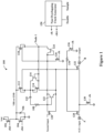
- a high voltage bootstrap sampling circuit may comprise transistors 102, 104, 112, 114, 116, 118, 120, 122, 124, 126, 128, 130, 132 and 136; Zener diode 106, capacitor 110, and resistors 108 and 134. Also included may be a non-overlapping clock generator 150 that may be used to generate low-voltage non-overlapping control signals (clocks), e.g., clock outputs "clk” and "clkb.”
- clocks low-voltage non-overlapping control signals
- Zener diode 106 is not strictly required, but can be included to prevent high-voltage kickback (when the switch transitions to the off-state) from damaging the low-voltage transistors also connected at this node.
- Capacitor 110 may be from about one (1) picofarad (pf) to about 20 pf and may be used to hold the DC voltage which is applied between the GATE and SOURCE of transistors 120, 128, and 132 (the actual switch transistors).
- Resistor 108 may be from about 0 ohms (unused) to about 100k ohms and may be used to slew-limit the off-on transition of the switch.
- Resistor 134 may be from about 0 ohms (unused) to about 100k ohms and may be used to slew-limit the on-off transition of the switch.
- the high voltage multiplexer 100 may accept a 0-32 VDC input at either terminal and provide a 0-32 VDC output, regardless of input voltage. All control voltages may be, for example but are not limited to, 5 VDC, 3.3 VDC or lower.
- the gate and source of switch transistors 120, 128 and 132 are released from GND by taking clk low which turns off transistor 136.
- the Bootstrap voltage input (the voltage driven by transistors 104 and 102) switches from VBS ( ⁇ 5 VDC) to GND.
- Transistor 114 forces VBS, e.g., 5 VDC, across Vgs of NMOS switch transistors 120, 128 and 132, thereby turning on transistors 120, 128 and 132, and making them conductive, whereby the high voltage bootstrap sampling circuit 100 is turned ON.
- VBS e.g., 5 VDC
- All transistors in the circuit are held at less than 5 VDC Vgs at all times (including transient voltages).
- NPN transistors 122 and 116 (which could also be diodes or diode-connected MOSFETs) are only necessary to suppress transient voltages which may exceed 5 VDC during transitions, and may not be necessary in all embodiments.
- a second input path, shown coupled to transistor 120, may be provided to reduce leakage error at high temperatures. The second input path would be driven by the same voltage as NODE A, or a voltage which is substantially similar (e.g., Vsense could be driven by Vbus).
- the Zener diode 106 is for protection against high-voltage kickback and may not be required in certain applications.
- the resistors 108 and 134 are for slew-rate limiting and may not be required for certain applications.
- Bipolar junction transistors (BJT) 116, 122 and 124 may be replaced with metal oxide semiconductor field effect transistor (MOSFET) devices connected in a "diode" configuration.
- Transistors 102 and 104 may be normal low voltage MOSFETs.
- Vdd is the voltage that will be forced across the high-voltage gate-source junction to turn on the switch. It may vary depending on the HV MOSFET technology but is typically between about 2 VDC to about 5 VDC.
- the output voltage node can be driven to a high level by another switch device, e.g., many of these switches can be connected in parallel and the OFF switches aren't damaged by a switched-ON voltage output.
- Switching of the high voltage bootstrap sampling circuit 100 is done without having to use high-voltage control signals.
- An inverter circuit comprising low-voltage transistors 102 and 104, may be controlled by a low-voltage control signal.
- the transistor 118 pulls down NODE 1 from VDD towards GND which provides sufficient voltage to turn on transistor 114.
- the primary switch transistors 120, 128 and 132 are enabled and will continue to boost the source node of these transistors via the floating capacitor 110 (which may be connected between their gate and source nodes via transistor 114) without need of any high-voltage control logic. Recall that transistor 114 is in its conductive "on" state at this point.
- a sacrificial input path comprising transistor(s) 120 (and optional bipolar transistor 122) may be provided to remove leakage current and switching current from the primary input path (transistors 128 and 132).
- the primary path through the switch (high voltage bootstrap sampling circuit 100) comprises two back-to-back HVNFET devices, transistors 128 and 132. It is desirable that all current flows through the primary path and is not diverted.
- a second input path may comprise transistor 120, nominally a replica of the primary path, and also a similar HVNFET, may be used to source the current necessary to drive the switching circuitry parasitic loads including gate capacitance associated with transistors 120, 128 and 132, and parasitic (bottom-plate) capacitance of the capacitor 110 as well as other parasitic loads (interconnections, etc.).
- This second input path also sources most of the device leakage current which can flow through transistors 118 and 124 that would otherwise need to be sourced from the primary path.
- the second input may be driven by a voltage similar in magnitude to that of the primary input coupled to transistor 128. This allows a different path for leakage currents and switching currents versus signal currents, reducing the current requirement from the primary input and shifting it to the secondary (proxy) input.
- the circuit may also be configured without this feature, in which case it looks like the circuit shown in Figure 2 . Also shown in Figure 2 , the diode connected BJTs have been replaced with high-voltage NMOSFET devices.
- the floating capacitor 110 may be alternately driven by either the primary (transistors 128 and 132) or the secondary input path (transistor 120).
- parasitic capacitance may be driven by the primary path for linearity and design simplicity. However, driving it via the second path would reduce loading on the primary input.
- circuit shown in Figure 1 may be used as a transmission-gate switch for high-voltage signals without requiring (1) a high voltage supply or (2) high voltage control signals, and (3) without consuming significant current from the input signal. It may be noted that diodes and overprotection circuitry may or may not be required in an actual implementation depending upon the manufacturing process.
- FIG. 2 depicted is a schematic diagram of a high voltage bootstrap sampling circuit, according to another specific example embodiment of this disclosure.
- the circuit shown in Figure 2 operates in substantially the same way as the circuit shown in Figure 1 and described hereinabove.
- This high voltage multiplexer 100 allows replica DC-offset calibration & offset dithering whereby a measured ⁇ 1 LSB (3 ⁇ V) input offset voltage is provided through the entire system (32 VDC range).
- the various embodiments further allow external resistor-capacitor (RC) filtering of inputs without corrupting measurement.
- Conventional devices warn of external resistors and printed circuit board (PCB) trace resistance corrupting measurements.
- PCB printed circuit board
- An evaluation board including a front-end device may include 100-Ohm series resistors on each input (not required). This allows a system user to place sense resistors close to generating circuitry where they make the most sense.
- FIG. 3 depicted is a schematic diagram of a sampling circuit with a single channel differential-input multiplexer comprising two high-voltage switches.
- a small differential voltage must be measured on top of a large common-mode voltage.
- the common-mode may be from about zero (0) VDC to about 32 VDC.
- the differential signal may be, for example, as small as +/-25 mV, for example, a voltage caused by a current through a sense resistor.
- the supply voltage for this circuit may be, for example but is not limited to, 2.6 VDC.
- eight inputs may be multiplexed, with each one having a different (unknown) common mode voltage V CM .
- the circuit shown in Figure 3 is an example of a switch-multiplexer that may be used in a higher-level system to measure a small differential voltage (at high VCM) and convert it to a larger low-voltage signal.
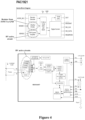
- FIG. 4 depicted are schematic block diagrams of prior technology sampling circuits.
- the prior technology sampling circuits shown in Figure 4 have no high-side voltage rail available, so power is taken from the input signal itself. Power taken from the input being measured is a key parameter.
- the PAC1921 manufactured by the Assignee of the present application uses no multiplexers and takes about 35 microamperes from each input channel.
- the PAC1720 (not shown) manufactured by the Assignee of the present application includes a two-channel multiplexer and takes about 150 microamperes from each input channel.
- a design target may be less than about one microampere with a four-channel multiplexer. A substantial improvement over prior technologies.
- the PAC1921 uses a resistor divider to measure the VBUS voltage (0-32v) by dividing it to a voltage between 0-3v.
- the PAC1921 uses a differential amplifier operating on the VBUS power supply to buffer the small differential voltage between VBUS and VSENSE and drive the resulting signal into a low-voltage ADC.
- the MAX34407 from the block diagram shown in Figure 4 , also includes an active high-voltage buffer operating from the external VBUS power supply.
- Present technology devices such as those shown in Figure 4 : a) comprise a differential input buffer amplifier powered from the high-side input (most common). The present technology amplifiers use DC current from the voltage input being measured and don't work down to zero (0) VDC. A source of channel-to-channel mismatch exists in these present technology devices. It is difficult to make bidirectional input since it is unknown which differential input carries the highest voltage; b) in some present technology devices, the switch transistor is powered from high-side input in such present technology devices and they use DC current from the input to create Vgs for the switch.
- some present technology devices use an AC-coupled switching control, which causes high variability, doesn't lend itself to a multiplexing configuration either, and is difficult to turn off as well (DC leakage can be high); and d) some present technology devices use a resistor-divider at the input, which uses DC current from the input, limits channel-to-channel matching to about 8 bits, and corrupts the signal-to-noise ratio (SNR).
- SNR signal-to-noise ratio
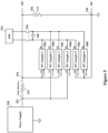
- FIG. 5 depicted is a schematic block diagram of a simplified example application of the high voltage bootstrap sampling circuits shown in Figures 1 and 2 , and adapted to couple current and voltage measurements of a power supply to a sampling circuit analog-to-digital converter (ADC), according the teachings of this disclosure.
- a plurality of high voltage bootstrap sampling circuits 100/200 may be coupled to a current sense resistor 542 and a power supply output voltage measured across a load (resistor) 550. Selected ones of the plurality of high voltage bootstrap sampling circuits 100/200 may connect different voltage nodes 552, 554 and 556 to a sample and hold capacitor 548.
- Two of the plurality of high voltage bootstrap sampling circuits 100/200 may be selected to couple plus and minus voltages of the voltage nodes to be measured to the sample and hold capacitor 548. Then these two bootstrap sampling circuits 100/200 are turned off (disconnected from the sample and hold capacitor 548), and the sample switch 546 is closed. Whereby the sampled voltage stored on the sample and hold capacitor 548 is coupled to a differential input (+/-) of an analog-to-digital convertor (ADC) 544 that may then convert the stored sampled voltage to a digital value that may be coupled to a microcontroller (not shown) for processing thereof.
- ADC analog-to-digital convertor
- the voltage drop across resistor 542 may be measured as either a positive voltage (high voltage sample circuits 100b and 100a enabled) or a negative voltage (high voltage sample circuits 100d and 100c enabled).
- the voltage supplied to the load may be measured as either a positive voltage (high voltage sample circuits 100c and 100e enabled) or a negative voltage (high voltage sample circuits 100a and 100f enabled).
- Bidirectional measurement capability e.g., plus (+) or minus (-) differential voltage measurements, may also be considered a desirable key parameter.
- Prior technology measurement circuits do not easily support bidirectional measurement without significant penalties in power consumption or complexity. It is difficult since one doesn't know which rail may carry the higher voltage potential and prior technology may depend on the higher (more positive) voltage potential for operating power.
- Another way of implementing a multiplexer is to first sample one voltage (VBUS) at node 370 (via switch 374) and store it onto capacitor 378 while the other capacitor 382 is reset to zero volts via switch 380. Then switch the other voltage (VSENSE) on node 372 (via switch 376) onto the capacitor 378 so the operational amplifier 384 will magnify the difference onto capacitor 382 via an N:1 capacitance ratio, for example an 8:1 capacitance ratio but is not limited to a specific capacitance ratio.
- VSENSE voltage
- N:1 capacitance ratio for example an 8:1 capacitance ratio but is not limited to a specific capacitance ratio.
- This high voltage multiplexer 100 allows replica DC-offset calibration & offset dithering wherein a measured ⁇ 1 LSB (3uV) input offset voltage is provided through the entire system (32 VDC range).
- the various embodiments further allow external resistor-capacitor (RC) filtering of inputs without corrupting measurement.
- Conventional devices warn of external resistors and printed circuit board (PCB) trace resistance corrupting measurements.
- PCB printed circuit board
- An evaluation board including a front-end device may include 100-Ohm series resistors on each input (not required). This allows a system user to place sense resistors close to generating circuitry where they make the most sense.
Landscapes
- Electronic Switches (AREA)
Applications Claiming Priority (3)
| Application Number | Priority Date | Filing Date | Title |
|---|---|---|---|
| US201662406881P | 2016-10-11 | 2016-10-11 | |
| US15/729,294 US10163521B2 (en) | 2016-10-11 | 2017-10-10 | High voltage bootstrap sampling circuit |
| PCT/US2017/056050 WO2018071479A1 (en) | 2016-10-11 | 2017-10-11 | High voltage bootstrap sampling circuit |
Publications (2)
| Publication Number | Publication Date |
|---|---|
| EP3526898A1 EP3526898A1 (en) | 2019-08-21 |
| EP3526898B1 true EP3526898B1 (en) | 2024-08-28 |
Family
ID=61829094
Family Applications (1)
| Application Number | Title | Priority Date | Filing Date |
|---|---|---|---|
| EP17791518.8A Active EP3526898B1 (en) | 2016-10-11 | 2017-10-11 | High voltage bootstrap sampling circuit |
Country Status (7)
| Country | Link |
|---|---|
| US (1) | US10163521B2 (enExample) |
| EP (1) | EP3526898B1 (enExample) |
| JP (1) | JP7061110B2 (enExample) |
| KR (1) | KR20190060755A (enExample) |
| CN (1) | CN109643992B (enExample) |
| TW (1) | TW201826711A (enExample) |
| WO (1) | WO2018071479A1 (enExample) |
Families Citing this family (11)
| Publication number | Priority date | Publication date | Assignee | Title |
|---|---|---|---|---|
| US10163521B2 (en) * | 2016-10-11 | 2018-12-25 | Microchip Technology Incorporated | High voltage bootstrap sampling circuit |
| US10686458B1 (en) * | 2017-08-01 | 2020-06-16 | Liming Xiu | Method and apparatus for improving frequency source frequency accuracy and frequency stability |
| US11699993B2 (en) * | 2020-09-15 | 2023-07-11 | Micron Technology, Inc. | Signal sampling with offset calibration |
| CN112636759A (zh) * | 2020-12-31 | 2021-04-09 | 成都思瑞浦微电子科技有限公司 | 一种采样电路 |
| KR102435395B1 (ko) * | 2021-02-25 | 2022-08-22 | 한국항공대학교산학협력단 | 높은 동적 입력 범위를 위한 샘플링 스위치 및 그의 구동 방법 |
| CN116027696B (zh) * | 2021-10-27 | 2024-12-17 | 中车株洲电力机车研究所有限公司 | 模拟量自适应采集装置、轨道交通信号采集系统及芯片 |
| US12512827B2 (en) * | 2022-08-05 | 2025-12-30 | Cirrus Logic Inc. | Beyond-the-rails bootstrapped sampling switch |
| US11979151B2 (en) | 2022-09-20 | 2024-05-07 | Nxp Usa, Inc. | Integrated circuit (IC) having an analog multiplexer (MUX) |
| CN115425958B (zh) * | 2022-11-04 | 2023-02-17 | 西安水木芯邦半导体设计有限公司 | 一种用于控制高压模拟开关的栅源电压保持电路 |
| CN116961655B (zh) * | 2023-09-21 | 2023-12-08 | 电子科技大学 | 一种应用于高精度adc的斩波采样电路 |
| US12470230B2 (en) | 2024-01-23 | 2025-11-11 | Cirrus Logic Inc. | Systems and methods for precharging driver circuitry for an analog-to-digital converter |
Citations (2)
| Publication number | Priority date | Publication date | Assignee | Title |
|---|---|---|---|---|
| EP2128633B1 (en) * | 2008-05-29 | 2012-05-02 | Austriamicrosystems AG | Current-sense amplifier arrangement and method for measuring a voltage signal |
| EP2173031B1 (en) * | 2008-10-01 | 2012-06-06 | Austriamicrosystems AG | Amplifier arrangement, measurement arrangement and signal processing method |
Family Cites Families (35)
| Publication number | Priority date | Publication date | Assignee | Title |
|---|---|---|---|---|
| US5603726A (en) * | 1989-09-22 | 1997-02-18 | Alfred E. Mann Foundation For Scientific Research | Multichannel cochlear implant system including wearable speech processor |
| US5531774A (en) * | 1989-09-22 | 1996-07-02 | Alfred E. Mann Foundation For Scientific Research | Multichannel implantable cochlear stimulator having programmable bipolar, monopolar or multipolar electrode configurations |
| US5938691A (en) * | 1989-09-22 | 1999-08-17 | Alfred E. Mann Foundation | Multichannel implantable cochlear stimulator |
| JPH05286150A (ja) * | 1992-03-05 | 1993-11-02 | Internatl Business Mach Corp <Ibm> | プリントハンマーコイル電流のモニタ回路及び制御回路 |
| US5572155A (en) * | 1994-06-20 | 1996-11-05 | Fuji Photo Film Co., Ltd. | CCD signal read-out circuit free from ailiasing of high-frequency noises |
| EP0729232B1 (en) * | 1995-02-22 | 2003-09-17 | Texas Instruments Incorporated | A high voltage analog switch |
| US6017273A (en) * | 1996-03-26 | 2000-01-25 | Pacific Digital Peripherals, Inc. | Joystick game adapter card for a personal computer |
| US5839959A (en) * | 1996-03-26 | 1998-11-24 | Pacific Digital Peripherals, Inc. | Joystick game adapter card for a personal computer |
| US6078311A (en) * | 1996-03-26 | 2000-06-20 | Pacific Digital Peripherals, Inc. | Joystick game adapter card for a personal computer |
| US6208542B1 (en) * | 1998-06-30 | 2001-03-27 | Sandisk Corporation | Techniques for storing digital data in an analog or multilevel memory |
| US6326740B1 (en) * | 1998-12-22 | 2001-12-04 | Philips Electronics North America Corporation | High frequency electronic ballast for multiple lamp independent operation |
| US6738275B1 (en) * | 1999-11-10 | 2004-05-18 | Electromed Internationale Ltee. | High-voltage x-ray generator |
| US8571179B2 (en) * | 1999-11-10 | 2013-10-29 | Robert Beland | Computed tomography systems |
| FR2818423B1 (fr) * | 2000-12-20 | 2003-04-04 | Chauvin Arnoux | Procede d'acquisition par echantillonage de signaux analogiques et systeme d'acquisition pour la mise en oeuvre de ce procede |
| KR100520682B1 (ko) | 2004-02-25 | 2005-10-11 | 주식회사 하이닉스반도체 | 반도체 소자의 고전압 스위치 회로 |
| US7176742B2 (en) | 2005-03-08 | 2007-02-13 | Texas Instruments Incorporated | Bootstrapped switch with an input dynamic range greater than supply voltage |
| US7479811B2 (en) * | 2005-09-08 | 2009-01-20 | Mediatek Inc. | Sample/hold circuit module |
| US7816951B1 (en) * | 2008-10-10 | 2010-10-19 | National Semiconductor Corporation | Locally boosted top plate sampling for a sampling capacitor |
| US8502594B2 (en) | 2008-12-31 | 2013-08-06 | Linear Technology Corporation | Bootstrap transistor circuit |
| US7952419B1 (en) | 2009-11-16 | 2011-05-31 | Analog Devices, Inc. | Bootstrapped switch circuit |
| CN102098034B (zh) * | 2009-12-15 | 2014-07-30 | 北京中星微电子有限公司 | 自举采样电路 |
| WO2012071733A1 (zh) * | 2010-12-02 | 2012-06-07 | 深圳矽睿芯科技有限公司 | 一种led驱动电源电路、驱动电源和照明装置 |
| US9084333B2 (en) * | 2010-12-08 | 2015-07-14 | Devtech Pte Ltd. | System for monitoring and controlling high intensity discharge (HID) lamps |
| US8299837B1 (en) * | 2011-08-16 | 2012-10-30 | Himax Technologies Limited | Integrator-based common mode stabilization method applied to pseudo-differential switched-capacitor circuit |
| KR20130072804A (ko) * | 2011-12-22 | 2013-07-02 | 에스케이하이닉스 주식회사 | 신호 샘플링 회로 및 이를 포함하는 이미지 센서 |
| US8810301B1 (en) * | 2012-06-22 | 2014-08-19 | Cadence Design Systems, Inc. | System and method for level shifting signals with adjustably controlled frequency response |
| JP6154705B2 (ja) * | 2013-09-24 | 2017-06-28 | 株式会社 日立パワーデバイス | 半導体スイッチ回路、信号処理装置、および、超音波診断装置 |
| US9178413B2 (en) * | 2013-11-19 | 2015-11-03 | Active-Semi, Inc. | Power factor correction autodetect |
| US9287862B2 (en) * | 2013-12-26 | 2016-03-15 | Texas Instruments Incorporated | Bootstrapped sampling switch circuits and systems |
| EP3105832A4 (en) * | 2014-02-14 | 2017-10-11 | Telefonaktiebolaget LM Ericsson (publ) | Power supply electronic circuit |
| US9576679B2 (en) * | 2014-10-09 | 2017-02-21 | Silicon Laboratories Inc. | Multi-stage sample and hold circuit |
| US10148174B2 (en) * | 2016-03-28 | 2018-12-04 | Qualcomm Incorporated | Duty cycle estimator for a switch mode power supply |
| US9906143B1 (en) * | 2016-09-30 | 2018-02-27 | Dell Products L.P. | Systems and methods for diagnostic current shunt and overcurrent protection (OCP) for power supplies |
| US10163521B2 (en) * | 2016-10-11 | 2018-12-25 | Microchip Technology Incorporated | High voltage bootstrap sampling circuit |
| US10034336B1 (en) * | 2017-09-22 | 2018-07-24 | Dialog Semiconductor (Uk) Limited | Controlling output voltage to achieve ultra-low standby power in dim-to-off LED applications |
-
2017
- 2017-10-10 US US15/729,294 patent/US10163521B2/en active Active
- 2017-10-11 JP JP2019506444A patent/JP7061110B2/ja active Active
- 2017-10-11 EP EP17791518.8A patent/EP3526898B1/en active Active
- 2017-10-11 WO PCT/US2017/056050 patent/WO2018071479A1/en not_active Ceased
- 2017-10-11 CN CN201780048465.6A patent/CN109643992B/zh active Active
- 2017-10-11 KR KR1020197003959A patent/KR20190060755A/ko not_active Withdrawn
- 2017-10-11 TW TW106134751A patent/TW201826711A/zh unknown
Patent Citations (2)
| Publication number | Priority date | Publication date | Assignee | Title |
|---|---|---|---|---|
| EP2128633B1 (en) * | 2008-05-29 | 2012-05-02 | Austriamicrosystems AG | Current-sense amplifier arrangement and method for measuring a voltage signal |
| EP2173031B1 (en) * | 2008-10-01 | 2012-06-06 | Austriamicrosystems AG | Amplifier arrangement, measurement arrangement and signal processing method |
Also Published As
| Publication number | Publication date |
|---|---|
| CN109643992B (zh) | 2023-07-25 |
| CN109643992A (zh) | 2019-04-16 |
| JP2019530278A (ja) | 2019-10-17 |
| US20180102180A1 (en) | 2018-04-12 |
| KR20190060755A (ko) | 2019-06-03 |
| EP3526898A1 (en) | 2019-08-21 |
| TW201826711A (zh) | 2018-07-16 |
| WO2018071479A1 (en) | 2018-04-19 |
| JP7061110B2 (ja) | 2022-04-27 |
| US10163521B2 (en) | 2018-12-25 |
Similar Documents
| Publication | Publication Date | Title |
|---|---|---|
| EP3526898B1 (en) | High voltage bootstrap sampling circuit | |
| US10826523B2 (en) | Analog-to-digital converter, measurement arrangement and method for analog-to-digital conversion | |
| US10564186B2 (en) | Current sense amplifier architecture and level shifter | |
| EP2128633B1 (en) | Current-sense amplifier arrangement and method for measuring a voltage signal | |
| US7746260B1 (en) | Multiplying digital-to-analog converter for high speed and low supply voltage | |
| CN108736849B (zh) | 低偏移电流感测放大器 | |
| US20140232387A1 (en) | Magnetic sensor device | |
| EP3621199B1 (en) | Instrumentation amplifier | |
| CN106257837B (zh) | 用于测试差分模/数转换器的方法及其对应系统 | |
| Jiang et al. | A low voltage low 1/f noise CMOS bandgap reference | |
| US10312865B2 (en) | Voltage range extension for difference amplifier | |
| EP3745148B1 (en) | High precision switched capacitor mosfet current measurement technique | |
| US20200186146A1 (en) | Sampling circuit and sampling method | |
| US11088667B2 (en) | Methods and apparatus for a dual mode operational amplifier | |
| US10333394B2 (en) | Switched-capacitor buffer and related methods | |
| JP4117976B2 (ja) | サンプルホールド回路 | |
| KR101939147B1 (ko) | 가변 기준전압 발생회로 및 이를 포함한 아날로그 디지털 변환기 | |
| US9673831B1 (en) | Passive switch having low leakage current | |
| CN118868928A (zh) | 高、低边高压采样接口电路 |
Legal Events
| Date | Code | Title | Description |
|---|---|---|---|
| STAA | Information on the status of an ep patent application or granted ep patent |
Free format text: STATUS: UNKNOWN |
|
| STAA | Information on the status of an ep patent application or granted ep patent |
Free format text: STATUS: THE INTERNATIONAL PUBLICATION HAS BEEN MADE |
|
| PUAI | Public reference made under article 153(3) epc to a published international application that has entered the european phase |
Free format text: ORIGINAL CODE: 0009012 |
|
| STAA | Information on the status of an ep patent application or granted ep patent |
Free format text: STATUS: REQUEST FOR EXAMINATION WAS MADE |
|
| 17P | Request for examination filed |
Effective date: 20190424 |
|
| AK | Designated contracting states |
Kind code of ref document: A1 Designated state(s): AL AT BE BG CH CY CZ DE DK EE ES FI FR GB GR HR HU IE IS IT LI LT LU LV MC MK MT NL NO PL PT RO RS SE SI SK SM TR |
|
| AX | Request for extension of the european patent |
Extension state: BA ME |
|
| DAV | Request for validation of the european patent (deleted) | ||
| DAX | Request for extension of the european patent (deleted) | ||
| STAA | Information on the status of an ep patent application or granted ep patent |
Free format text: STATUS: EXAMINATION IS IN PROGRESS |
|
| 17Q | First examination report despatched |
Effective date: 20200717 |
|
| GRAP | Despatch of communication of intention to grant a patent |
Free format text: ORIGINAL CODE: EPIDOSNIGR1 |
|
| STAA | Information on the status of an ep patent application or granted ep patent |
Free format text: STATUS: GRANT OF PATENT IS INTENDED |
|
| INTG | Intention to grant announced |
Effective date: 20240326 |
|
| RIN1 | Information on inventor provided before grant (corrected) |
Inventor name: MEACHAM, DAN |
|
| GRAS | Grant fee paid |
Free format text: ORIGINAL CODE: EPIDOSNIGR3 |
|
| GRAA | (expected) grant |
Free format text: ORIGINAL CODE: 0009210 |
|
| STAA | Information on the status of an ep patent application or granted ep patent |
Free format text: STATUS: THE PATENT HAS BEEN GRANTED |
|
| AK | Designated contracting states |
Kind code of ref document: B1 Designated state(s): AL AT BE BG CH CY CZ DE DK EE ES FI FR GB GR HR HU IE IS IT LI LT LU LV MC MK MT NL NO PL PT RO RS SE SI SK SM TR |
|
| REG | Reference to a national code |
Ref country code: GB Ref legal event code: FG4D |
|
| REG | Reference to a national code |
Ref country code: CH Ref legal event code: EP |
|
| REG | Reference to a national code |
Ref country code: DE Ref legal event code: R096 Ref document number: 602017084482 Country of ref document: DE |
|
| REG | Reference to a national code |
Ref country code: IE Ref legal event code: FG4D |
|
| REG | Reference to a national code |
Ref country code: LT Ref legal event code: MG9D |
|
| PG25 | Lapsed in a contracting state [announced via postgrant information from national office to epo] |
Ref country code: NO Free format text: LAPSE BECAUSE OF FAILURE TO SUBMIT A TRANSLATION OF THE DESCRIPTION OR TO PAY THE FEE WITHIN THE PRESCRIBED TIME-LIMIT Effective date: 20241128 |
|
| REG | Reference to a national code |
Ref country code: AT Ref legal event code: MK05 Ref document number: 1719084 Country of ref document: AT Kind code of ref document: T Effective date: 20240828 |
|
| PG25 | Lapsed in a contracting state [announced via postgrant information from national office to epo] |
Ref country code: NL Free format text: LAPSE BECAUSE OF FAILURE TO SUBMIT A TRANSLATION OF THE DESCRIPTION OR TO PAY THE FEE WITHIN THE PRESCRIBED TIME-LIMIT Effective date: 20240828 Ref country code: GR Free format text: LAPSE BECAUSE OF FAILURE TO SUBMIT A TRANSLATION OF THE DESCRIPTION OR TO PAY THE FEE WITHIN THE PRESCRIBED TIME-LIMIT Effective date: 20241129 Ref country code: PT Free format text: LAPSE BECAUSE OF FAILURE TO SUBMIT A TRANSLATION OF THE DESCRIPTION OR TO PAY THE FEE WITHIN THE PRESCRIBED TIME-LIMIT Effective date: 20241230 Ref country code: PL Free format text: LAPSE BECAUSE OF FAILURE TO SUBMIT A TRANSLATION OF THE DESCRIPTION OR TO PAY THE FEE WITHIN THE PRESCRIBED TIME-LIMIT Effective date: 20240828 Ref country code: FI Free format text: LAPSE BECAUSE OF FAILURE TO SUBMIT A TRANSLATION OF THE DESCRIPTION OR TO PAY THE FEE WITHIN THE PRESCRIBED TIME-LIMIT Effective date: 20240828 |
|
| PG25 | Lapsed in a contracting state [announced via postgrant information from national office to epo] |
Ref country code: BG Free format text: LAPSE BECAUSE OF FAILURE TO SUBMIT A TRANSLATION OF THE DESCRIPTION OR TO PAY THE FEE WITHIN THE PRESCRIBED TIME-LIMIT Effective date: 20240828 |
|
| PG25 | Lapsed in a contracting state [announced via postgrant information from national office to epo] |
Ref country code: LV Free format text: LAPSE BECAUSE OF FAILURE TO SUBMIT A TRANSLATION OF THE DESCRIPTION OR TO PAY THE FEE WITHIN THE PRESCRIBED TIME-LIMIT Effective date: 20240828 |
|
| REG | Reference to a national code |
Ref country code: NL Ref legal event code: MP Effective date: 20240828 |
|
| PG25 | Lapsed in a contracting state [announced via postgrant information from national office to epo] |
Ref country code: AT Free format text: LAPSE BECAUSE OF FAILURE TO SUBMIT A TRANSLATION OF THE DESCRIPTION OR TO PAY THE FEE WITHIN THE PRESCRIBED TIME-LIMIT Effective date: 20240828 Ref country code: IS Free format text: LAPSE BECAUSE OF FAILURE TO SUBMIT A TRANSLATION OF THE DESCRIPTION OR TO PAY THE FEE WITHIN THE PRESCRIBED TIME-LIMIT Effective date: 20241228 |
|
| PG25 | Lapsed in a contracting state [announced via postgrant information from national office to epo] |
Ref country code: HR Free format text: LAPSE BECAUSE OF FAILURE TO SUBMIT A TRANSLATION OF THE DESCRIPTION OR TO PAY THE FEE WITHIN THE PRESCRIBED TIME-LIMIT Effective date: 20240828 |
|
| PG25 | Lapsed in a contracting state [announced via postgrant information from national office to epo] |
Ref country code: RS Free format text: LAPSE BECAUSE OF FAILURE TO SUBMIT A TRANSLATION OF THE DESCRIPTION OR TO PAY THE FEE WITHIN THE PRESCRIBED TIME-LIMIT Effective date: 20241128 Ref country code: ES Free format text: LAPSE BECAUSE OF FAILURE TO SUBMIT A TRANSLATION OF THE DESCRIPTION OR TO PAY THE FEE WITHIN THE PRESCRIBED TIME-LIMIT Effective date: 20240828 |
|
| PG25 | Lapsed in a contracting state [announced via postgrant information from national office to epo] |
Ref country code: RS Free format text: LAPSE BECAUSE OF FAILURE TO SUBMIT A TRANSLATION OF THE DESCRIPTION OR TO PAY THE FEE WITHIN THE PRESCRIBED TIME-LIMIT Effective date: 20241128 Ref country code: PT Free format text: LAPSE BECAUSE OF FAILURE TO SUBMIT A TRANSLATION OF THE DESCRIPTION OR TO PAY THE FEE WITHIN THE PRESCRIBED TIME-LIMIT Effective date: 20241230 Ref country code: PL Free format text: LAPSE BECAUSE OF FAILURE TO SUBMIT A TRANSLATION OF THE DESCRIPTION OR TO PAY THE FEE WITHIN THE PRESCRIBED TIME-LIMIT Effective date: 20240828 Ref country code: NO Free format text: LAPSE BECAUSE OF FAILURE TO SUBMIT A TRANSLATION OF THE DESCRIPTION OR TO PAY THE FEE WITHIN THE PRESCRIBED TIME-LIMIT Effective date: 20241128 Ref country code: NL Free format text: LAPSE BECAUSE OF FAILURE TO SUBMIT A TRANSLATION OF THE DESCRIPTION OR TO PAY THE FEE WITHIN THE PRESCRIBED TIME-LIMIT Effective date: 20240828 Ref country code: LV Free format text: LAPSE BECAUSE OF FAILURE TO SUBMIT A TRANSLATION OF THE DESCRIPTION OR TO PAY THE FEE WITHIN THE PRESCRIBED TIME-LIMIT Effective date: 20240828 Ref country code: IS Free format text: LAPSE BECAUSE OF FAILURE TO SUBMIT A TRANSLATION OF THE DESCRIPTION OR TO PAY THE FEE WITHIN THE PRESCRIBED TIME-LIMIT Effective date: 20241228 Ref country code: HR Free format text: LAPSE BECAUSE OF FAILURE TO SUBMIT A TRANSLATION OF THE DESCRIPTION OR TO PAY THE FEE WITHIN THE PRESCRIBED TIME-LIMIT Effective date: 20240828 Ref country code: GR Free format text: LAPSE BECAUSE OF FAILURE TO SUBMIT A TRANSLATION OF THE DESCRIPTION OR TO PAY THE FEE WITHIN THE PRESCRIBED TIME-LIMIT Effective date: 20241129 Ref country code: FI Free format text: LAPSE BECAUSE OF FAILURE TO SUBMIT A TRANSLATION OF THE DESCRIPTION OR TO PAY THE FEE WITHIN THE PRESCRIBED TIME-LIMIT Effective date: 20240828 Ref country code: ES Free format text: LAPSE BECAUSE OF FAILURE TO SUBMIT A TRANSLATION OF THE DESCRIPTION OR TO PAY THE FEE WITHIN THE PRESCRIBED TIME-LIMIT Effective date: 20240828 Ref country code: BG Free format text: LAPSE BECAUSE OF FAILURE TO SUBMIT A TRANSLATION OF THE DESCRIPTION OR TO PAY THE FEE WITHIN THE PRESCRIBED TIME-LIMIT Effective date: 20240828 Ref country code: AT Free format text: LAPSE BECAUSE OF FAILURE TO SUBMIT A TRANSLATION OF THE DESCRIPTION OR TO PAY THE FEE WITHIN THE PRESCRIBED TIME-LIMIT Effective date: 20240828 |
|
| PG25 | Lapsed in a contracting state [announced via postgrant information from national office to epo] |
Ref country code: RO Free format text: LAPSE BECAUSE OF FAILURE TO SUBMIT A TRANSLATION OF THE DESCRIPTION OR TO PAY THE FEE WITHIN THE PRESCRIBED TIME-LIMIT Effective date: 20240828 Ref country code: SM Free format text: LAPSE BECAUSE OF FAILURE TO SUBMIT A TRANSLATION OF THE DESCRIPTION OR TO PAY THE FEE WITHIN THE PRESCRIBED TIME-LIMIT Effective date: 20240828 Ref country code: DK Free format text: LAPSE BECAUSE OF FAILURE TO SUBMIT A TRANSLATION OF THE DESCRIPTION OR TO PAY THE FEE WITHIN THE PRESCRIBED TIME-LIMIT Effective date: 20240828 |
|
| PG25 | Lapsed in a contracting state [announced via postgrant information from national office to epo] |
Ref country code: EE Free format text: LAPSE BECAUSE OF FAILURE TO SUBMIT A TRANSLATION OF THE DESCRIPTION OR TO PAY THE FEE WITHIN THE PRESCRIBED TIME-LIMIT Effective date: 20240828 |
|
| PG25 | Lapsed in a contracting state [announced via postgrant information from national office to epo] |
Ref country code: CZ Free format text: LAPSE BECAUSE OF FAILURE TO SUBMIT A TRANSLATION OF THE DESCRIPTION OR TO PAY THE FEE WITHIN THE PRESCRIBED TIME-LIMIT Effective date: 20240828 |
|
| PG25 | Lapsed in a contracting state [announced via postgrant information from national office to epo] |
Ref country code: IT Free format text: LAPSE BECAUSE OF FAILURE TO SUBMIT A TRANSLATION OF THE DESCRIPTION OR TO PAY THE FEE WITHIN THE PRESCRIBED TIME-LIMIT Effective date: 20240828 Ref country code: SK Free format text: LAPSE BECAUSE OF FAILURE TO SUBMIT A TRANSLATION OF THE DESCRIPTION OR TO PAY THE FEE WITHIN THE PRESCRIBED TIME-LIMIT Effective date: 20240828 |
|
| REG | Reference to a national code |
Ref country code: CH Ref legal event code: PL Ref country code: DE Ref legal event code: R097 Ref document number: 602017084482 Country of ref document: DE |
|
| PLBE | No opposition filed within time limit |
Free format text: ORIGINAL CODE: 0009261 |
|
| STAA | Information on the status of an ep patent application or granted ep patent |
Free format text: STATUS: NO OPPOSITION FILED WITHIN TIME LIMIT |
|
| PG25 | Lapsed in a contracting state [announced via postgrant information from national office to epo] |
Ref country code: MC Free format text: LAPSE BECAUSE OF FAILURE TO SUBMIT A TRANSLATION OF THE DESCRIPTION OR TO PAY THE FEE WITHIN THE PRESCRIBED TIME-LIMIT Effective date: 20240828 |
|
| PG25 | Lapsed in a contracting state [announced via postgrant information from national office to epo] |
Ref country code: BE Free format text: LAPSE BECAUSE OF NON-PAYMENT OF DUE FEES Effective date: 20241031 Ref country code: LU Free format text: LAPSE BECAUSE OF NON-PAYMENT OF DUE FEES Effective date: 20241011 |
|
| PG25 | Lapsed in a contracting state [announced via postgrant information from national office to epo] |
Ref country code: FR Free format text: LAPSE BECAUSE OF NON-PAYMENT OF DUE FEES Effective date: 20241028 |
|
| GBPC | Gb: european patent ceased through non-payment of renewal fee |
Effective date: 20241128 |
|
| PG25 | Lapsed in a contracting state [announced via postgrant information from national office to epo] |
Ref country code: CH Free format text: LAPSE BECAUSE OF NON-PAYMENT OF DUE FEES Effective date: 20241031 |
|
| 26N | No opposition filed |
Effective date: 20250530 |
|
| REG | Reference to a national code |
Ref country code: BE Ref legal event code: MM Effective date: 20241031 |
|
| PG25 | Lapsed in a contracting state [announced via postgrant information from national office to epo] |
Ref country code: SE Free format text: LAPSE BECAUSE OF FAILURE TO SUBMIT A TRANSLATION OF THE DESCRIPTION OR TO PAY THE FEE WITHIN THE PRESCRIBED TIME-LIMIT Effective date: 20240828 |
|
| PG25 | Lapsed in a contracting state [announced via postgrant information from national office to epo] |
Ref country code: GB Free format text: LAPSE BECAUSE OF NON-PAYMENT OF DUE FEES Effective date: 20241128 |
|
| PG25 | Lapsed in a contracting state [announced via postgrant information from national office to epo] |
Ref country code: IE Free format text: LAPSE BECAUSE OF NON-PAYMENT OF DUE FEES Effective date: 20241011 |
|
| PGFP | Annual fee paid to national office [announced via postgrant information from national office to epo] |
Ref country code: DE Payment date: 20250923 Year of fee payment: 9 |
|
| PG25 | Lapsed in a contracting state [announced via postgrant information from national office to epo] |
Ref country code: CY Free format text: LAPSE BECAUSE OF FAILURE TO SUBMIT A TRANSLATION OF THE DESCRIPTION OR TO PAY THE FEE WITHIN THE PRESCRIBED TIME-LIMIT; INVALID AB INITIO Effective date: 20171011 |
|
| PG25 | Lapsed in a contracting state [announced via postgrant information from national office to epo] |
Ref country code: HU Free format text: LAPSE BECAUSE OF FAILURE TO SUBMIT A TRANSLATION OF THE DESCRIPTION OR TO PAY THE FEE WITHIN THE PRESCRIBED TIME-LIMIT; INVALID AB INITIO Effective date: 20171011 |