EP3512097B1 - Ausgabeschaltkreis und ausgabeverfahren - Google Patents
Ausgabeschaltkreis und ausgabeverfahren Download PDFInfo
- Publication number
- EP3512097B1 EP3512097B1 EP18199738.8A EP18199738A EP3512097B1 EP 3512097 B1 EP3512097 B1 EP 3512097B1 EP 18199738 A EP18199738 A EP 18199738A EP 3512097 B1 EP3512097 B1 EP 3512097B1
- Authority
- EP
- European Patent Office
- Prior art keywords
- transistor
- current
- turned
- base
- output circuit
- Prior art date
- Legal status (The legal status is an assumption and is not a legal conclusion. Google has not performed a legal analysis and makes no representation as to the accuracy of the status listed.)
- Active
Links
Images



Classifications
-
- H—ELECTRICITY
- H03—ELECTRONIC CIRCUITRY
- H03K—PULSE TECHNIQUE
- H03K17/00—Electronic switching or gating, i.e. not by contact-making and –breaking
- H03K17/04—Modifications for accelerating switching
- H03K17/042—Modifications for accelerating switching by feedback from the output circuit to the control circuit
-
- H—ELECTRICITY
- H03—ELECTRONIC CIRCUITRY
- H03K—PULSE TECHNIQUE
- H03K17/00—Electronic switching or gating, i.e. not by contact-making and –breaking
- H03K17/04—Modifications for accelerating switching
- H03K17/041—Modifications for accelerating switching without feedback from the output circuit to the control circuit
- H03K17/0412—Modifications for accelerating switching without feedback from the output circuit to the control circuit by measures taken in the control circuit
- H03K17/04126—Modifications for accelerating switching without feedback from the output circuit to the control circuit by measures taken in the control circuit in bipolar transistor switches
-
- H—ELECTRICITY
- H03—ELECTRONIC CIRCUITRY
- H03K—PULSE TECHNIQUE
- H03K17/00—Electronic switching or gating, i.e. not by contact-making and –breaking
- H03K17/04—Modifications for accelerating switching
-
- H—ELECTRICITY
- H03—ELECTRONIC CIRCUITRY
- H03K—PULSE TECHNIQUE
- H03K17/00—Electronic switching or gating, i.e. not by contact-making and –breaking
- H03K17/04—Modifications for accelerating switching
- H03K17/041—Modifications for accelerating switching without feedback from the output circuit to the control circuit
- H03K17/0412—Modifications for accelerating switching without feedback from the output circuit to the control circuit by measures taken in the control circuit
- H03K17/0414—Anti-saturation measures
-
- H—ELECTRICITY
- H03—ELECTRONIC CIRCUITRY
- H03K—PULSE TECHNIQUE
- H03K17/00—Electronic switching or gating, i.e. not by contact-making and –breaking
- H03K17/51—Electronic switching or gating, i.e. not by contact-making and –breaking characterised by the components used
- H03K17/56—Electronic switching or gating, i.e. not by contact-making and –breaking characterised by the components used by the use, as active elements, of semiconductor devices
-
- H—ELECTRICITY
- H03—ELECTRONIC CIRCUITRY
- H03K—PULSE TECHNIQUE
- H03K17/00—Electronic switching or gating, i.e. not by contact-making and –breaking
- H03K17/51—Electronic switching or gating, i.e. not by contact-making and –breaking characterised by the components used
- H03K17/56—Electronic switching or gating, i.e. not by contact-making and –breaking characterised by the components used by the use, as active elements, of semiconductor devices
- H03K17/60—Electronic switching or gating, i.e. not by contact-making and –breaking characterised by the components used by the use, as active elements, of semiconductor devices the devices being bipolar transistors
-
- H—ELECTRICITY
- H04—ELECTRIC COMMUNICATION TECHNIQUE
- H04B—TRANSMISSION
- H04B1/00—Details of transmission systems, not covered by a single one of groups H04B3/00 - H04B13/00; Details of transmission systems not characterised by the medium used for transmission
- H04B1/02—Transmitters
- H04B1/04—Circuits
Definitions
- the present invention relates to an output circuit and an output method.
- the following output circuit in which an emitter and a collector of a PNP transistor are connected between a base and an emitter of a base input transistor, when the base input transistor using input signals is turned off, the PNP transistor is driven to be turned on to form a desired current path, and base accumulated charges of the base input transistor are discharged via the PNP transistor (see patent literature 1 [ Japanese Laid-open No. 60-213121 ]).
- the output circuit discharges the base accumulated charges of the base input transistor and forms the current path by one PNP transistor, and thus number of elements can be reduced compared with a case in which circuit elements corresponding to respective purposes are arranged.
- Document US 4 847 520 discloses a circuit for reducing the turn-off transition time of a switching PNP transistor by providing a reverse drive current to the base of the PNP transistor after the drive current has been removed from the base.
- the reverse drive current is generated by an NPN transistor, the emitter of which is connected to the base of the PNP transistor.
- a capacitor coupled to the base of the NPN transistor is charged and during the conducting period of the PNP transistor and discharged after the drive current is removed from the base of the PNP transistor to enable the base of the NPN transistor to be driven above the supply voltage connected to the emitter of the PNP transistor.
- Document US 5 903 425 discloses a control circuit for providing fast turn-off of a PNP transistor with output transient protection.
- An embodiment of the invention provides a current amplifier coupled between a positive voltage supply line and the base of a PNP switching transistor and an input device for providing an input current to the current amplifier.
- the current amplifier provides a transitory reverse drive current to the base of the PNP switching transistor.
- the current amplifier and the input device both include transient blocking junctions that block current flow from a positive voltage transient in excess of the positive supply voltage.
- Document US 5 128 553 discloses an integrated circuit is provided which uses a single drive signal for turning a PNP switching transistor "on” and “off.”
- An NPN transistor provides reverse drive current to the PNP transistor's base. When the drive signal is present, the PNP switching transistor is turned “on” and is driven into saturation. The drive signal during this period also charges an integrated capacitor coupled to the base of the NPN transistor. The drive signal then is removed to turn the PNP transistor “off.” Removal of the drive signal also causes the voltage developed across the capacitor to drive the base of the NPN transistor. This, in turn, causes the NPN transistor to drive the base of the PNP transistor with a reverse drive current, thus speeding up the switching of the PNP transistor from the conducting state to the non-conducting state.
- the output circuit provided with a PNP transistor outputs a collector current of the PNP transistor as communication signals and communicates with an external device, in order to achieve high-speed communication, it is necessary to switch between the ON state and OFF state of the PNP transistor in a short time.
- the PNP transistor has a property that the turn-off time before the OFF state is reached depends on a charge amount accumulated in the base during the ON state (referred to as "base accumulated charge amount” hereinafter).
- the present invention aims to provide an output circuit and an output method capable of shortening the turn-off time of a transistor.
- the output circuit of one aspect of the present invention is an output circuit that outputs communication signals and communicates with an external device and includes: a PNP first transistor, which is capable of outputting a collector current as the communication signals; and a first current source, which is capable of changing a base current of the first transistor, and reduces the base current to a predetermined current value after the first transistor is turned on and before the first transistor is turned off.
- the base current is reduced to the predetermined current value. Accordingly, compared with a case in which the base current is fixed when the first transistor is on, the base accumulated charge amount of the first transistor can be reduced. Therefore, the turn-off time of the first transistor can be shortened, and the decrease in the communication speed with the external device can be suppressed. Besides, compared with a push-pull configuration for example, which is provided with a PNP transistor on a high side and a NPN transistor on a low side, the number of components (number of elements) can be reduced, and the output circuit can be miniaturized.
- the predetermined current value may be 1/r (r is a real number over 2) of the current value of the base current when the first transistor is turned on.
- the predetermined current value is 1/r of the current value of the base current when the first transistor is turned on. Accordingly, an output circuit which reduces the base accumulated charge amount of the first transistor can be easily realized.
- a switch connected between a base and an emitter of the first transistor may be further included, and the switch is turned on when the first transistor is turned off.
- the switch when the first transistor is turned off, the switch is turned on. Accordingly, due to a resistance between the base and the emitter of the first transistor, the base accumulated charge amount of the first transistor can be discharged rapidly. Therefore, the turn-off time of the first transistor can be further shortened.
- a second current source which supplies a constant current to the base of the first transistor when the first transistor is turned off, may be further included.
- the turn-off time of the first transistor can be further shortened.
- a second transistor which is connected to a signal line outputting the communication signals and a reference potential line, and which is turned on when the first transistor is turned off, may be further included.
- the second transistor when the first transistor is turned off, the second transistor is turned on.
- the signal line and the reference potential line are lines connected to an external device, and an inter-line parasitic capacity between the signal line and the reference potential line may be generated.
- the inter-line parasitic capacity causes the time, which is required for the collector potential to reach a Low level after the first transistor is turned off, to be delayed. Therefore, by turning on the second transistor when the first transistor is turned off, the inter-line parasitic capacity between the signal line and the reference potential line can be discharged. Therefore, the time for the collector potential to reach the Low level after the first transistor is turned off can be accelerated.
- a third current source which applies a constant current flows between the signal line and the reference potential line, may be further included.
- a constant current flows between the signal line and the reference potential line. Accordingly, even when the second transistor is turned off, a constant current still flows between the signal line and the reference potential line, and thus the inter-line parasitic capacity between the signal line and the reference potential line can be reduced. Therefore, the time for the collector potential to reach the Low level after the first transistor is turned off can be accelerated.
- the output circuit may have a COM mode for communicating with the external device and a SIO mode for supplying a load current to the external device, and in the SIO mode, the first transistor is capable of outputting the collector current as the load current.
- the first transistor in the SIO mode, is capable of outputting the collector current as the load current. Accordingly, the output circuit can make the two modes compatible, that is, in the COM mode, the output circuit communicates with the external device, and in the SIO mode, the output circuit supplies the load current to a high-load external device.
- the output method of another aspect of the present invention is an output method of an output circuit that outputs communication signals and communicates with an external device, and the output method includes a step in which a first current source, which is capable of changing a base current of a PNP first transistor, reduces the base current to a predetermined current value after the first transistor is turned on and before the first transistor is turned off, wherein the PNP first transistor is capable of outputting a collector current as the communication signals.
- the base current is reduced to the predetermined current value. Accordingly, compared with a case in which the base current is fixed when the first transistor is on, the base accumulated charge amount of the first transistor can be reduced. Therefore, the turn-off time of the first transistor is shortened, and the decrease in the communication speed with the external device can be suppressed. Besides, compared with a push-pull configuration for example, which is provided with a PNP transistor on a high side and a NPN transistor on a low side, the number of components (number of elements) can be reduced, and the output circuit can be miniaturized.
- a step may be further included in which a switch connected between a base and an emitter of the first transistor is turned on when the first transistor is turned off.
- the first transistor switch connected between the base and the emitter of the first transistor is turned on. Accordingly, due to a resistance between the base and the emitter of the first transistor, the base accumulated charge amount of the first transistor can be discharged rapidly. Therefore, the turn-off time of the first transistor can be further shortened.
- a step may be further included in which a second current source supplies a constant current to the base of the first transistor when the first transistor is turned off.
- the turn-off time of the first transistor can be further shortened.
- a step may further included in which a second transistor connected to a signal line outputting the communication signals and a reference potential line is turned on when the first transistor is turned off.
- the second transistor connected to the signal line outputting the communication signals and the reference potential line is turned on.
- the signal line and the reference potential line are lines connected to the external device, and an inter-line parasitic capacity between the signal line and the reference potential line may be generated.
- the inter-line parasitic capacity causes a discharge time to be lengthened when the base accumulated charge amount of the first transistor is discharged. Therefore, by turning on the second transistor when the first transistor is turned off, the inter-line parasitic capacity between the signal line and the reference potential line can be discharged. Therefore, the discharge time of the base accumulated charge amount of the first transistor can be shortened.
- a step may be further included in which a third current source applies a constant current between the signal line and the reference potential line.
- a constant current flows between the signal line and the reference potential line. Accordingly, even when the second transistor is turned off, a constant current still flows between the signal line and the reference potential line, and thus the inter-line parasitic capacity between the signal line and the reference potential line can be reduced. Therefore, the discharge time of the base accumulated charge amount of the first transistor can be shortened.
- the output circuit and the output method capable of shortening the turn-off time of the transistor can be provided.
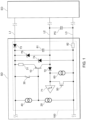
- FIG. 1 is a circuit diagram illustrating a configuration of an output circuit 100 of the embodiment.
- a sensor device SD includes the output circuit 100 as an input-output interface.
- the output circuit 100 is used to output communication signals and communicate with an external device ED.
- the output circuit 100 communicates in accordance with IO-Link that is a communication standard for field apparatus such as a sensor, an actuator and the like.
- IO-Link has a COM mode for performing digital communication of data (information) and a SIO mode for performing digital communication of ON/OFF (binary information).
- the COM mode is used in, for example, a case in which a master machine is connected as the external device ED and data of the sensor device SD is transmitted to the external device ED.
- three kinds of communication speeds namely COM1: 4.8k [bps], COM2: 38.4k [bps], COM1: 230.4k [bps] are specified.
- the SIO mode is used in, for example, a case in which another device machine is connected as the external device ED and a load current is supplied to the external device ED.
- the sensor device SD is connected to the external device ED via a power line L1, a signal line L2, and a reference potential line L3.
- the three lines can be extended up to 20 meters at most.
- the output circuit 100 functions (serves) as an output interface of the sensor device SD, but the present invention is not limited thereto.
- the output circuit 100 may also function (serve) as an input interface of the sensor device SD. In this case, signals are input from the external device ED to the output circuit 100 via the signal line L2.
- the output circuit 100 includes a first transistor 10, a first current source 20, a switch 30, a first resistor 31, a second current source 40, a second transistor 50, a third current source 60, a comparator 71, a first diode 72, a second diode 73, a third diode 74, a fourth diode 75, a capacitor 81, and a second resistor 82.
- the first transistor 10 is configured to be capable of outputting a collector current as a communication signal of the output circuit 100 in the COM mode. Besides, the first transistor 10 is configured to be capable of outputting the collector current as a load current supplied by the output circuit 100 in the SIO mode. Accordingly, the output circuit 100 can make the two modes compatible, that is, in the COM mode, the output circuit 100 communicates with the external device ED, and in the SIO mode, the output circuit 100 supplies the load current to the high-load external device ED.
- the first transistor 10 is a PNP bipolar transistor, and has the switching function and the function of current amplification.
- An emitter of the first transistor 10 is connected to the power line L1 via the first resistor 31.
- the first resistor 31 is used to detect, by a voltage, an over current flowing in the first resistor 31 when the connected load is short circuited, and prevent the damage of the first transistor 10 due to the over current.
- a collector of the first transistor 10 is connected to the signal line L2. Accordingly, the first transistor 10 can output the collector current to the external device ED via the signal line L2. That is, the output circuit 100 is an open-collector output circuit using the first transistor 10.
- the first transistor 10 which is a PNP transistor accumulates a base accumulated charge amount between the base and the emitter in an ON state. Besides, the first transistor 10 has a property that the turn-off time before the OFF state is reached depends on the charge amount.
- the first current source 20 is configured to be capable of changing the base current of the first transistor 10. Specifically, the first current source 20 is connected between the base of the first transistor 10 and the reference potential line L3. The first current source 20 operates based on a control signal input from a control part (not illustrated) of the sensor device SD. Besides, the first current source 20 reduces the base current to a predetermined current value after the first transistor 10 is turned on and before the first transistor 10 is turned off, and the detail is described later.
- the predetermined current value is 1/r of the current value of the base current when the first transistor 10 is turned on (r is a real number over 2).
- One end of the switch 30 is connected to the base of the first transistor 10, and the other end is connected to the power line L1 via the second diode 73. Accordingly, the switch 30 is connected between the base and the emitter of the first transistor 10 via the first resistor 31.
- the switch 30 switches to ON or OFF based on the control signal input from the control part of the sensor device SD. Besides, the switch 30 is turned on when the first transistor 10 is turned off, and the detail is described later.
- the second current source 40 is configured to be capable of supply a constant current to the base of the first transistor 10. Specifically, the second current source 40 is connected between the base of the first transistor 10 and the power line L1 through the second diode 73. The second current source 40 starts or stops supplying a constant current to the base of the first transistor 10 based on the control signal input from the control part of the sensor device SD. Besides, the second current source 40 supplies a constant current to the base of the first transistor 10 when the first transistor 10 is turned off, and the detail is described later.
- the second transistor 50 is an N-channel MOSFET (Meta1-Oxide-Semicdonductor Field-Effect Transistor).
- a drain of the second transistor 50 is connected to the signal line L2 via the first diode 72, and a source is connected to the reference potential line L3 via the second resistor 82.
- the control signal is input from the control part of the sensor device SD to a gate of the second transistor 50, and the second transistor 50 is turned on or off based on a voltage of the control signal.
- the second transistor 50 is turned on when the first transistor is turned off, and the detail is described later.
- the signal line L2 and the reference potential line L3 are lines connected to the external device ED, and the line is 20 meters at most. Therefore, an inter-line parasitic capacity PC exists between the signal line L2 and the reference potential line L3.
- An internal parasitic capacity of the sensor device SD is 1 [nF] at most; in contrast, the inter-line parasitic capacity PC is 3 [nF] at most. Therefore, the inter-line parasitic capacity PC is dominant in the whole parasitic capacity and cannot be ignored.
- the inter-line parasitic capacity PC causes the time, which is required for the collector potential to reach a Low level after the first transistor 10 is turned off, to be delayed.
- the third current source 60 is configured so as to apply a constant current between the signal line L2 and the reference potential line L3. Specifically, the third current source 60 applies a constant current flowing from the signal line L2 to the reference potential line L3.
- the comparator 71 is configured so as to detect a reception signal (reception data) input from the external device ED via the signal line L2.
- the signal line L2 is connected to a non-inverting input terminal, and a reference voltage source is connected to an inverting input terminal.
- the comparator 71 When a voltage value of the reception signal input via the signal line L2 is above the voltage value of the reference voltage source, the comparator 71 outputs a detection signal having a relatively high voltage value (referred to as "H level” hereinafter).
- H level relatively high voltage value
- the comparator 71 outputs a detection signal having a relatively low voltage value (referred to as "L level” hereinafter).
- the first diode 72 is used to prevent an over voltage from being input to the signal line L2.
- the second diode 73 is used to make sure that the current does not flow when the connection to the power line L1 is incorrect (reverse connection protection).
- the third diode 74 is used to absorb the noise generated between the power line L1 and the reference potential line L3 (protection from input of a surge current).
- the fourth diode 75 is used to absorb the noise generated between the power line L1 and the signal line L2 (protection from input of a surge current).
- Zener diodes are usually used as the third diode 74 and the fourth diode 75.
- the capacitor 81 and the second resistor 82 form an integration circuit.
- the capacitor 81 is used to smooth a power supply voltage and is connected to the power line L1 and the reference potential line L3.
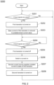
- FIG. 2 is a flowchart illustrating a schematic operation in the COM mode of the output circuit 100.
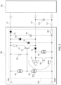
- FIG. 3 is a circuit diagram illustrating the operation when the first transistor 10 is turned on.
- FIG. 4 is a circuit diagram illustrating the operation when the base current of the first transistor 10 is reduced.
- FIG. 5 is a circuit diagram illustrating the operation when the first transistor 10 is turned off.
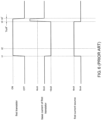
- FIG. 6 is a timing chart illustrating the operation of an existing output circuit.
- FIG. 7 is a timing chart illustrating the operation of the output circuit 100 of the embodiment.
- the sensor device SD when the SIO mode is switched to the COM mode by inputting the control signal from the external device ED via the signal line L2, the sensor device SD performs a COM mode processing S200 shown in FIG. 2 .
- the sensor device SD determines whether an H level signal is output from the output circuit 100 (S201).
- the sensor device SD repeats step S201 until an H level signal is input from the output circuit 100.
- the output circuit 100 outputs an L level signal.
- step S201 When the determination result of step S201 is that an H level signal is output from the output circuit 100, the sensor device SD outputs a control signal to drive the first current source 20, and the first transistor 10 is turned on (S202).
- the first current source 20 starts based on an input control signal Sc1 and sucks the base current of the first transistor 10. That is, a sink current Isink shown by a solid line arrow flows.
- the sink current Isink flows, the potential of the base of the first transistor 10 decreases; as a result, when a voltage Vbe between the base and the emitter is larger than the predetermined value, the first transistor 10 is turned on. Accordingly, the collector current of the first transistor 10 can be output via the signal line L2, and H level signals are output from the output circuit 100.
- the sensor device SD outputs control signals to the first current source 20 in the state that a power supply voltage is applied between the power line L1 and the reference potential line L3, and the first current source 20 reduces the base current to the predetermined current value (S203).
- the first current source 20 reduces the base current to the predetermined current value based on an input control signal Sc2. That is, a sink current Isink' shown by a broken line arrow flows.
- the voltage Vbe between the base and the emitter of the first transistor 10 becomes fixed or substantially fixed regardless of the current value of the base current. Accordingly, when the first transistor 10 is turned on, even if the first current source 20 reduces the base current to the predetermined current value, the ON state of the first transistor 10 is maintained.
- the sensor device SD determines whether an L level signal is output from the output circuit 100 (S204).
- the sensor device SD repeats step S204 until an L level signal is output from the output circuit 100. That is, the sensor device SD outputs H level signals until an L level signal is output from the output circuit 100.
- step S204 When the determination result of step S204 is that an L level signal is output from the output circuit 100, the sensor device SD outputs a control signal to stop the first current source 20, and the first transistor 10 is turned off (S205).
- the sensor device SD outputs a control signal to turn the switch 30 on (S206). Moreover, after step S206, when a predetermined time passed, the sensor device SD outputs a control signal to turn the switch 30 off.
- the sensor device SD outputs a control signal to drive the second current source 40, and supplies a constant current to the base of the first transistor 10 (S207).
- the sensor device SD outputs a control signal to turn the second transistor 50 on (S208). Moreover, after step S208, when the predetermined time passed, the sensor device SD outputs a control signal to turn the second transistor 50 off.
- step S208 the sensor device SD returns to step S201 again, and repeats step S201 to step S208 until, for example, the COM mode is switched to the SIO mode.
- step S205 to step S208 are performed in sequence, but the present invention is not limited thereto.
- the sequence of steps S205-S208 may be changed.
- steps S205-S208 are performed simultaneously (at the same timing).
- the first current source 20 stops based on an input control signal Sc3. That is, the sink current Isink' shown in FIG. 4 does not flow.
- the potential of the base of the first transistor 10 increases; as a result, when the voltage Vbe between the base and the emitter is below the predetermined value, the first transistor 10 is turned off. Accordingly, because the collector current of the first transistor 10 does not flow, an L level signal is output from the output circuit 100.
- the operation of an existing output circuit is described for comparison.
- the first transistor in time t1, the first transistor is turned on, and thus the first current source starts to apply a current of 4 [mA] for example, and sucks the base current of the first transistor. Therefore, the base current of the first transistor becomes -4 [mA]. Because the first current source applies a current of 4 [mA] until the first transistor is turned off at time t3, the base current of the first transistor maintains -4 [mA]. In addition, because the first transistor is turned off at time t3, the first current source stops and the current value becomes 0 [mA].
- the PNP transistor has a property that the turn-off time depends on the base accumulated charge amount accumulated in the base during the ON state. In the example shown in FIG. 6 , in time t3, the first transistor is about to be turned off, but in fact there is a delay between time t3 and time t4' at which the first transistor is actually turned off, and the time between time t3 and time t4' is a turn-off time Ttoff.
- the first current source 20 in order to turn the first transistor 10 on at time t1, the first current source 20 starts to apply a current of 4 [mA] for example, and sucks the base current of the first transistor 10. Therefore, the base current of the first transistor becomes -4 [mA]. Then, at time t2, the first current source 20 reduces the base current to the predetermined current value of -0.8 [mA] for example.
- the predetermined current value is 1/5 of -4 [mA], which is the current value of the base current when the first transistor 10 is turned on.
- the first current source 20 applies a current of 0.8 [mA] until the first transistor 10 is turned off at time t3, and maintains the base current of the first transistor 10 at -0.8 [mA]. Then, in order to turn the first transistor 10 off at time t3, the first current source 20 stops and the current value thereof becomes 0 [mA].
- the first transistor 10 is about to be turned off at time t3, but in fact there is a delay between time t3 and time t4 at which the first transistor 10 is actually turned off, and the time between time t3 and time t4 is a turn-off time Ttoff.
- the turn-off time Ttoff is shorter than the turn-off time Ttoff shown in FIG. 6 (turn-off time Ttoff ⁇ turn-off time Ttoff).
- the base accumulated charge amount of the first transistor 10 can be reduced compared with the case in which the base current is fixed during the ON state of the first transistor 10. Therefore, the turn-off time Ttoff of the first transistor 10 can be shortened, and a decrease in the communication speed with the external device ED can be suppressed.
- the number of components can be reduced, and the output circuit 100 can be miniaturized.
- the predetermined current value of the base current reduced by the first current source 20 is 1/r (r is a real number over 2) of the current value of the base current when the first transistor 10 is turned on. Accordingly, the output circuit 100 which reduces the base accumulated charge amount of the first transistor 10 can be easily realized.
- the switch 30 is turned on based on the input control signal Sc4. At this time, a discharge current Idis1 shown by a solid line arrow flows. Accordingly, due to the resistance of the first resistor 31 and the like between the base and the emitter of the first transistor 10, the base accumulated charge amount of the first transistor 10 can be discharged rapidly. Therefore, the turn-off time Ttoff of the first transistor 10 can be further shortened.
- the second current source 40 applies the constant current to the base of the first transistor 10 based on the input control signal Sc5.
- a reverse current Irev shown by a solid line arrow flows. Accordingly, due to the reverse current supplied to the base of the first transistor 10, the base accumulated charge amount of the first transistor 10 is discharged rapidly. Therefore, the turn-off time Ttoff of the first transistor 10 can be further shortened.
- the second transistor 50 is turned on based on, for example, a control signal Sc6 input to a gate. At this time, a discharge current Idis2 shown by a solid line arrow flows. Accordingly, the inter-line parasitic capacity PC between the signal line L2 and the reference potential line L3 can be discharged. Therefore, the time required for the collector potential to reach a Low level after the first transistor 10 is turned off can be accelerated.
- the third current source 60 applies a constant current between the signal line L2 and the reference potential line L3 regardless of the ON state or OFF state of the first transistor 10. Accordingly, even when the second transistor 50 is turned off at time t5 for example, the constant current still flows between the signal line L2 and the reference potential line L3, and thus the inter-line parasitic capacity PC between the signal line L2 and the reference potential line L3 can be reduced. Therefore, the time required for the collector potential to reach a Low level after the first transistor 10 is turned off can be accelerated.
- the example is described in which the first current source 20 reduces the base current to 1/5 of the current value of the base current when the first transistor 10 is turned on, but the present invention is not limited thereto.
- the output circuit 100 supplies two times of load current to the external device ED in the SIO mode
- the first current source 20 reduces the base current to 1/10 of the current value of the base current when the first transistor 10 is turned on, similar to the above-mentioned example, the base accumulated charge amount of the first transistor 10 can be reduced, and the turn-off time Ttoff of the first transistor 10 can be shortened.
- the base current can be reduced to the predetermined current value. Accordingly, compared with a case in which the base current is fixed during the ON state of the first transistor 10, the base accumulated charge amount of the first transistor 10 can be reduced. Therefore, the turn-off time Ttoff of the first transistor 10 can be shortened, and a decrease in the communication speed with the external device ED can be suppressed. Besides, compared with a push-pull configuration for example, which is provided with a PNP transistor on a high side and a NPN transistor on a low side, the number of components (number of elements) can be reduced, and the output circuit 100 can be miniaturized.
Landscapes
- Engineering & Computer Science (AREA)
- Computer Networks & Wireless Communication (AREA)
- Signal Processing (AREA)
- Electronic Switches (AREA)
Claims (7)
- Ausgabeschaltung (100), die konfiguriert ist, um Kommunikationssignale an eine externe Vorrichtung (ED) in einem Kommunikationsmodus auszugeben und konfiguriert ist, um einen Laststrom an die externe Vorrichtung (ED) in einem seriellen Eingabe-/Ausgabemodus zuzuführen, wobei die Ausgabeschaltung (100) umfasst:einen ersten Transistor (10), der vom PNP-Typ ist, wobei der erste Transistor (10) fähig ist, einen Kollektorstrom als die Kommunikationssignale in dem Kommunikationsmodus auszugeben und einen Kollektorstrom als den Laststrom in dem seriellen Eingabe-/Ausgabemodus zuzuführen; wobei der erste Transistor (10) einen Basisanschluss, einen Emitteranschluss und einen Kollektoranschluss umfasst;eine erste Stromquelle (20), die in dem Kommunikationsmodus konfiguriert ist, einen Basisstrom des ersten Transistors (10) basierend auf einem Eingabesteuersignal (Sc3) zu ändern, wobei, als Antwort auf die Ausgabeschaltung (100), die ein Hochpegelsignal ausgibt, die erste Stromquelle (20) konfiguriert ist, einen Sinkstrom (Isink) bereitzustellen, um den Basisstrom des ersten Transistors (10) zu reduzieren, um den ersten Transistor (10) einzuschalten, und wobei, als Antwort auf die Ausgabeschaltung (100), die ein niedriges Pegelsignal ausgibt, die erste Stromquelle (20) konfiguriert ist, Zuführen des Sinkstroms (Isink) zu stoppen, um den ersten Transistor (10) auszuschalten,wobei die erste Stromquelle (20) in dem seriellen Eingabe-/Ausgabemodus ferner konfiguriert ist, um den Basisstrom auf einem vorbestimmten Stromwert zu reduzieren, nachdem der erste Transistor (10) eingeschalten ist, und bevor der erste Transistor (10) ausgeschalten ist, der erste Transistor (10), den Kollektorstrom als den Laststrom ausgibt,wobei die erste Stromquelle (20) zwischen dem Basisanschluss des ersten Transistors (10) und einer Referenzpotenzialleitung (L3) gekoppelt ist;eine zweite Stromquelle (40), die konfiguriert ist, um einen konstanten Strom an die Basis des ersten Transistors (10) zuzuführen, wenn der erste Transistor (10) ausgeschalten ist;einen zweiten Transistor (50), der mit einer Signalleitung (L2) verbunden ist, die die Kommunikationssignale und eine Referenzpotenzialleitung (L3) ausgibt, und die konfiguriert ist, eingeschalten zu werden, wenn der erste Transistor (10) ausgeschalten ist, undeine Diode (72), die eine Anode und eine Kathode aufweist, die jeweils mit der Signalleitung (L2) und einem Abfluss des zweiten Transistors (50) gekoppelt sind,wobei, durch Einschalten des zweiten Transistors (50), wenn der erste Transistor (10) ausgeschalten ist, eine Zwischenleitungs-parasitäre-Kapazität zwischen der Signalleitung (L2) und einer Referenzpotenzialleitung (L3) entladen ist, so dass die Zeit zum Entladen des Kollektorstroms in den ersten Transistor (10) beschleunigt ist.
- Ausgabeschaltung (100) gemäß Anspruch 1, wobei der vorbestimmte Stromwert 1/r eines Stromwertes des Basisstroms ist, wenn der erste Transistor (10) eingeschaltet ist, wobei r eine reelle Zahl über 2 ist.
- Ausgabeschaltung (100) gemäß Anspruch 1 oder 2, ferner umfassend einen Schalter (30), der zwischen einer Basis und einem Emitter des ersten Transistors (10) verbunden ist, wobei der Schalter (30) eingeschaltet ist, wenn der erste Transistor (10) ausgeschalten ist.
- Ausgabeschaltung (100) gemäß einem der Ansprüche 1 bis 3, ferner umfassend eine dritte Stromquelle (60), die einen konstanten Strom zwischen der Signalleitung (L2) und der Referenzpotentialleitung (L3) anlegt.
- Ausgabeverfahren, das das Ausgabeverfahren einer Ausgabeschaltung (100) ist, die konfiguriert ist, um Kommunikationssignale an eine externen Vorrichtung (ED) in einem Kommunikationsmodus auszugeben und konfiguriert ist, um einen Laststrom an die externe Vorrichtung (ED) in einem seriellen Eingabe-/Ausgabemodus zuzuführen, wobei das Verfahren umfasst:einen Schritt (S203), in demeine erste Stromquelle (20), die in dem Kommunikationsmodus konfiguriert ist, einen Basisstrom eines ersten Transistors (10), der vom PNP-Typ ist, basierend auf einem Eingabesteuersignal (Sc3) zu ändern, wobei als Antwort auf die Ausgabeschaltung (100), die ein Hochpegelsignal ausgibt, die erste Stromquelle (20) konfiguriert ist, einen Sinkstrom (Isink) bereitzustellen, um den Basisstrom des ersten Transistors (10) zu reduzieren, um den ersten Transistor (10) einzuschalten, und wobei als Antwort auf die Ausgabeschaltung (100), die ein niedriges Pegelsignal ausgibt, die erste Stromquelle (20) konfiguriert ist, um Zuführen des Sinkstroms (Isink) zu stoppen, um den ersten Transistor (10) auszuschalten,wobei die erste Stromquelle (20), die in dem seriellen Eingabe-/Ausgabemodus ferner konfiguriert ist, einen Basisstrom auf einen vorbestimmten Wert zu reduzieren, nachdem der erste Transistor (10) eingeschalten ist und bevor der erste Transistor (10) ausgeschalten ist, der erste Transistor (10), den Kollektorstrom als den Laststrom ausgibt, wobei der erste Transistor (10) in der Lage ist, einen Kollektorstrom als die Kommunikationssignale auszugeben,wobei der erste Transistor (10) einen Basisanschluss, einen Emitteranschluss und einen Kollektoranschluss umfasst,wobei die erste Stromquelle (20) zwischen dem Basisanschluss des ersten Transistors (10) und einer Referenzpotenzialleitung (L3) gekoppelt ist:einen Schritt (S207), bei dem eine zweite Stromquelle (40) einen konstanten Strom an die Basis des ersten Transistors (10) zuführt, wenn der erste Transistor (10) ausgeschalten ist, und einen Schritt (S208), bei dem ein zweiter Transistor (50), der mit einer Signalleitung (L2), die die Kommunikationssignale ausgibt, und einer Referenzpotentialleitung (L3) verbunden ist, eingeschalten wird, wenn der erste Transistor (10) ausgeschalten ist, und eine Anode und eine Kathode einer Diode (72), die j eweils mit einer Signalleitung (L2) und einem Abfluss des zweiten Transistors (50) gekoppelt sind,wobei, durch Einschalten des zweiten Transistors (50), wenn der erste Transistor (10) ausgeschalten wird, eine Zwischenleitungs-parasitäre-Kapazität zwischen der Signalleitung (L2) und der Referenzpotenzialleitung (L3) entladen wird, sodass die Zeit zum Entladen des Kollektorstroms in den ersten Transistor (10) beschleunigt wird.
- Ausgabeverfahren gemäß Anspruch 5, ferner umfassend einen Schritt (S206) in dem ein Schalter (30) zwischen einer Basis und einem Emitter des ersten Transistors (10) eingeschalten wird, wenn der erste Transistor (10) ausgeschalten wird.
- Ausgabeverfahren gemäß Anspruch 5 oder 6, das ferner einen Schritt umfasst, bei dem eine dritte Stromquelle (60) einen konstanten Strom zwischen der Signalleitung (L2) und der Referenzpotentialleitung (L3) anlegt.
Applications Claiming Priority (1)
| Application Number | Priority Date | Filing Date | Title |
|---|---|---|---|
| JP2018002674A JP6880511B2 (ja) | 2018-01-11 | 2018-01-11 | 出力回路及び出力方法 |
Publications (2)
| Publication Number | Publication Date |
|---|---|
| EP3512097A1 EP3512097A1 (de) | 2019-07-17 |
| EP3512097B1 true EP3512097B1 (de) | 2024-03-13 |
Family
ID=63833848
Family Applications (1)
| Application Number | Title | Priority Date | Filing Date |
|---|---|---|---|
| EP18199738.8A Active EP3512097B1 (de) | 2018-01-11 | 2018-10-10 | Ausgabeschaltkreis und ausgabeverfahren |
Country Status (5)
| Country | Link |
|---|---|
| US (1) | US10425072B2 (de) |
| EP (1) | EP3512097B1 (de) |
| JP (1) | JP6880511B2 (de) |
| KR (1) | KR102069852B1 (de) |
| CN (1) | CN110034751B (de) |
Families Citing this family (1)
| Publication number | Priority date | Publication date | Assignee | Title |
|---|---|---|---|---|
| US20240113542A1 (en) * | 2021-01-27 | 2024-04-04 | Panasonic Energy Co., Ltd. | Power supply device |
Family Cites Families (20)
| Publication number | Priority date | Publication date | Assignee | Title |
|---|---|---|---|---|
| JPS56131213A (en) * | 1980-02-07 | 1981-10-14 | Sanyo Electric Co Ltd | Current miller circuit |
| JPS60199219A (ja) * | 1983-12-20 | 1985-10-08 | フエアチアイルド カメラ アンド インストルメント コ−ポレ−シヨン | 飽和したトランジスタの蓄積時間を減少させる方法及び装置 |
| JPS60213121A (ja) | 1984-04-06 | 1985-10-25 | Hitachi Ltd | 出力回路 |
| JPH0732336B2 (ja) * | 1986-03-21 | 1995-04-10 | ソニー株式会社 | スイツチング電流発生回路 |
| US4847520A (en) * | 1987-08-31 | 1989-07-11 | Linear Technology Corporation | Fast PNP transistor turn-off circuit |
| US5128553A (en) * | 1990-06-22 | 1992-07-07 | Linear Technology Corporation | Lateral PNP turn-off drive circuit |
| JP2989439B2 (ja) | 1993-07-22 | 1999-12-13 | 東海興業株式会社 | コンクリ−ト型枠のシール構造、及びこれを構成するパッキング |
| US5903140A (en) * | 1995-07-26 | 1999-05-11 | Bensys, Inc. | Low dissipation controllable electron valve |
| JP3562141B2 (ja) * | 1996-06-18 | 2004-09-08 | 株式会社デンソー | 電流出力回路 |
| US5903425A (en) * | 1997-06-02 | 1999-05-11 | Cherry Semiconductor Corporation | Lateral PNP fast turn-off circuit |
| JP2000031827A (ja) | 1998-07-09 | 2000-01-28 | Sony Corp | 電流出力回路 |
| JP3627671B2 (ja) * | 2001-05-28 | 2005-03-09 | 日産自動車株式会社 | 電流制御型素子用駆動装置 |
| JP2003199328A (ja) * | 2001-12-27 | 2003-07-11 | Sony Corp | スイッチ回路 |
| JP2005136560A (ja) | 2003-10-29 | 2005-05-26 | Toshiba Corp | 出力回路 |
| US7394316B1 (en) * | 2006-08-31 | 2008-07-01 | Texas Instruments Incorporated | High speed, high current gain voltage buffer and method |
| JP2010190604A (ja) | 2009-02-16 | 2010-09-02 | Toyota Motor Corp | 端子開放検出装置及び半導体装置 |
| CN103152023A (zh) * | 2013-02-06 | 2013-06-12 | 苏州硅智源微电子有限公司 | 快速pnp晶体管关断电路 |
| JP6102377B2 (ja) * | 2013-03-15 | 2017-03-29 | オムロン株式会社 | センサ |
| JP6758029B2 (ja) | 2015-07-09 | 2020-09-23 | ローム株式会社 | 半導体装置 |
| JP7032336B2 (ja) * | 2019-01-17 | 2022-03-08 | 株式会社ウナム | 車両タイヤ用防滑具 |
-
2018
- 2018-01-11 JP JP2018002674A patent/JP6880511B2/ja active Active
- 2018-10-10 KR KR1020180120499A patent/KR102069852B1/ko active Active
- 2018-10-10 EP EP18199738.8A patent/EP3512097B1/de active Active
- 2018-10-15 CN CN201811196201.8A patent/CN110034751B/zh active Active
- 2018-10-16 US US16/161,103 patent/US10425072B2/en active Active
Also Published As
| Publication number | Publication date |
|---|---|
| JP6880511B2 (ja) | 2021-06-02 |
| KR102069852B1 (ko) | 2020-01-23 |
| CN110034751B (zh) | 2023-02-21 |
| EP3512097A1 (de) | 2019-07-17 |
| JP2019122009A (ja) | 2019-07-22 |
| CN110034751A (zh) | 2019-07-19 |
| KR20190085832A (ko) | 2019-07-19 |
| US20190214978A1 (en) | 2019-07-11 |
| US10425072B2 (en) | 2019-09-24 |
Similar Documents
| Publication | Publication Date | Title |
|---|---|---|
| US10186946B2 (en) | Switching element driving device | |
| US6819149B2 (en) | Gate drive device for reducing a surge voltage and switching loss | |
| US10110221B1 (en) | Power transistor control signal gating | |
| US10476496B2 (en) | Drive circuit and power module including the same | |
| US8537515B2 (en) | Driving circuit and semiconductor device with the driving circuit | |
| US7362147B2 (en) | Integrated circuit | |
| EP3832866B1 (de) | Überstromschutzschaltung und schaltkreis | |
| US7274227B2 (en) | Power-on reset circuit | |
| US7705638B2 (en) | Switching control circuit with reduced dead time | |
| US6741116B2 (en) | Semiconductor component for direct gate control and monitoring of power semiconductor switches | |
| EP3512097A1 (de) | Ausgabeschaltkreis und ausgabeverfahren | |
| US6924694B2 (en) | Switch circuit | |
| JP2002204154A (ja) | 終端回路およびその方法 | |
| JP2009145170A (ja) | 温度センサ回路 | |
| JP2007173823A (ja) | 入力電圧感知回路 | |
| JP2005192350A (ja) | 降圧式チャージポンプタイプ型電源回路およびモノリシック集積回路 | |
| US6037802A (en) | Tristate buffer having a bipolar transistor | |
| EP0645890B1 (de) | BICMOS-Logikschaltung | |
| CN112531646B (zh) | 一种过压保护电路及方法、以及开关电源 | |
| EP1101286B1 (de) | Pegelumsetzer mit anstiegszeitsteurungsvorrichtung | |
| US7564231B2 (en) | Switching power supply source | |
| JP7161509B2 (ja) | ゲート駆動回路 | |
| CN119739239B (zh) | 一种芯片的电源控制电路和芯片 | |
| US20060145671A1 (en) | Circuit for preventing latch-up in DC-DC converter | |
| US20260086966A1 (en) | Uart communications device with power management circuit |
Legal Events
| Date | Code | Title | Description |
|---|---|---|---|
| PUAI | Public reference made under article 153(3) epc to a published international application that has entered the european phase |
Free format text: ORIGINAL CODE: 0009012 |
|
| STAA | Information on the status of an ep patent application or granted ep patent |
Free format text: STATUS: REQUEST FOR EXAMINATION WAS MADE |
|
| 17P | Request for examination filed |
Effective date: 20181010 |
|
| AK | Designated contracting states |
Kind code of ref document: A1 Designated state(s): AL AT BE BG CH CY CZ DE DK EE ES FI FR GB GR HR HU IE IS IT LI LT LU LV MC MK MT NL NO PL PT RO RS SE SI SK SM TR |
|
| AX | Request for extension of the european patent |
Extension state: BA ME |
|
| RBV | Designated contracting states (corrected) |
Designated state(s): AL AT BE BG CH CY CZ DE DK EE ES FI FR GB GR HR HU IE IS IT LI LT LU LV MC MK MT NL NO PL PT RO RS SE SI SK SM TR |
|
| STAA | Information on the status of an ep patent application or granted ep patent |
Free format text: STATUS: EXAMINATION IS IN PROGRESS |
|
| 17Q | First examination report despatched |
Effective date: 20200803 |
|
| GRAP | Despatch of communication of intention to grant a patent |
Free format text: ORIGINAL CODE: EPIDOSNIGR1 |
|
| STAA | Information on the status of an ep patent application or granted ep patent |
Free format text: STATUS: GRANT OF PATENT IS INTENDED |
|
| INTG | Intention to grant announced |
Effective date: 20231102 |
|
| GRAS | Grant fee paid |
Free format text: ORIGINAL CODE: EPIDOSNIGR3 |
|
| GRAA | (expected) grant |
Free format text: ORIGINAL CODE: 0009210 |
|
| STAA | Information on the status of an ep patent application or granted ep patent |
Free format text: STATUS: THE PATENT HAS BEEN GRANTED |
|
| AK | Designated contracting states |
Kind code of ref document: B1 Designated state(s): AL AT BE BG CH CY CZ DE DK EE ES FI FR GB GR HR HU IE IS IT LI LT LU LV MC MK MT NL NO PL PT RO RS SE SI SK SM TR |
|
| REG | Reference to a national code |
Ref country code: GB Ref legal event code: FG4D |
|
| REG | Reference to a national code |
Ref country code: CH Ref legal event code: EP |
|
| REG | Reference to a national code |
Ref country code: DE Ref legal event code: R096 Ref document number: 602018066506 Country of ref document: DE |
|
| REG | Reference to a national code |
Ref country code: IE Ref legal event code: FG4D |
|
| PG25 | Lapsed in a contracting state [announced via postgrant information from national office to epo] |
Ref country code: LT Free format text: LAPSE BECAUSE OF FAILURE TO SUBMIT A TRANSLATION OF THE DESCRIPTION OR TO PAY THE FEE WITHIN THE PRESCRIBED TIME-LIMIT Effective date: 20240313 |
|
| REG | Reference to a national code |
Ref country code: LT Ref legal event code: MG9D |
|
| PG25 | Lapsed in a contracting state [announced via postgrant information from national office to epo] |
Ref country code: GR Free format text: LAPSE BECAUSE OF FAILURE TO SUBMIT A TRANSLATION OF THE DESCRIPTION OR TO PAY THE FEE WITHIN THE PRESCRIBED TIME-LIMIT Effective date: 20240614 |
|
| REG | Reference to a national code |
Ref country code: NL Ref legal event code: MP Effective date: 20240313 |
|
| PG25 | Lapsed in a contracting state [announced via postgrant information from national office to epo] |
Ref country code: RS Free format text: LAPSE BECAUSE OF FAILURE TO SUBMIT A TRANSLATION OF THE DESCRIPTION OR TO PAY THE FEE WITHIN THE PRESCRIBED TIME-LIMIT Effective date: 20240613 Ref country code: HR Free format text: LAPSE BECAUSE OF FAILURE TO SUBMIT A TRANSLATION OF THE DESCRIPTION OR TO PAY THE FEE WITHIN THE PRESCRIBED TIME-LIMIT Effective date: 20240313 |
|
| PG25 | Lapsed in a contracting state [announced via postgrant information from national office to epo] |
Ref country code: ES Free format text: LAPSE BECAUSE OF FAILURE TO SUBMIT A TRANSLATION OF THE DESCRIPTION OR TO PAY THE FEE WITHIN THE PRESCRIBED TIME-LIMIT Effective date: 20240313 |
|
| PG25 | Lapsed in a contracting state [announced via postgrant information from national office to epo] |
Ref country code: RS Free format text: LAPSE BECAUSE OF FAILURE TO SUBMIT A TRANSLATION OF THE DESCRIPTION OR TO PAY THE FEE WITHIN THE PRESCRIBED TIME-LIMIT Effective date: 20240613 Ref country code: NO Free format text: LAPSE BECAUSE OF FAILURE TO SUBMIT A TRANSLATION OF THE DESCRIPTION OR TO PAY THE FEE WITHIN THE PRESCRIBED TIME-LIMIT Effective date: 20240613 Ref country code: LT Free format text: LAPSE BECAUSE OF FAILURE TO SUBMIT A TRANSLATION OF THE DESCRIPTION OR TO PAY THE FEE WITHIN THE PRESCRIBED TIME-LIMIT Effective date: 20240313 Ref country code: HR Free format text: LAPSE BECAUSE OF FAILURE TO SUBMIT A TRANSLATION OF THE DESCRIPTION OR TO PAY THE FEE WITHIN THE PRESCRIBED TIME-LIMIT Effective date: 20240313 Ref country code: GR Free format text: LAPSE BECAUSE OF FAILURE TO SUBMIT A TRANSLATION OF THE DESCRIPTION OR TO PAY THE FEE WITHIN THE PRESCRIBED TIME-LIMIT Effective date: 20240614 Ref country code: FI Free format text: LAPSE BECAUSE OF FAILURE TO SUBMIT A TRANSLATION OF THE DESCRIPTION OR TO PAY THE FEE WITHIN THE PRESCRIBED TIME-LIMIT Effective date: 20240313 Ref country code: ES Free format text: LAPSE BECAUSE OF FAILURE TO SUBMIT A TRANSLATION OF THE DESCRIPTION OR TO PAY THE FEE WITHIN THE PRESCRIBED TIME-LIMIT Effective date: 20240313 Ref country code: BG Free format text: LAPSE BECAUSE OF FAILURE TO SUBMIT A TRANSLATION OF THE DESCRIPTION OR TO PAY THE FEE WITHIN THE PRESCRIBED TIME-LIMIT Effective date: 20240313 |
|
| REG | Reference to a national code |
Ref country code: AT Ref legal event code: MK05 Ref document number: 1666710 Country of ref document: AT Kind code of ref document: T Effective date: 20240313 |
|
| PG25 | Lapsed in a contracting state [announced via postgrant information from national office to epo] |
Ref country code: SE Free format text: LAPSE BECAUSE OF FAILURE TO SUBMIT A TRANSLATION OF THE DESCRIPTION OR TO PAY THE FEE WITHIN THE PRESCRIBED TIME-LIMIT Effective date: 20240313 Ref country code: LV Free format text: LAPSE BECAUSE OF FAILURE TO SUBMIT A TRANSLATION OF THE DESCRIPTION OR TO PAY THE FEE WITHIN THE PRESCRIBED TIME-LIMIT Effective date: 20240313 |
|
| PG25 | Lapsed in a contracting state [announced via postgrant information from national office to epo] |
Ref country code: NL Free format text: LAPSE BECAUSE OF FAILURE TO SUBMIT A TRANSLATION OF THE DESCRIPTION OR TO PAY THE FEE WITHIN THE PRESCRIBED TIME-LIMIT Effective date: 20240313 |
|
| PG25 | Lapsed in a contracting state [announced via postgrant information from national office to epo] |
Ref country code: NL Free format text: LAPSE BECAUSE OF FAILURE TO SUBMIT A TRANSLATION OF THE DESCRIPTION OR TO PAY THE FEE WITHIN THE PRESCRIBED TIME-LIMIT Effective date: 20240313 |
|
| PG25 | Lapsed in a contracting state [announced via postgrant information from national office to epo] |
Ref country code: IS Free format text: LAPSE BECAUSE OF FAILURE TO SUBMIT A TRANSLATION OF THE DESCRIPTION OR TO PAY THE FEE WITHIN THE PRESCRIBED TIME-LIMIT Effective date: 20240713 |
|
| PG25 | Lapsed in a contracting state [announced via postgrant information from national office to epo] |
Ref country code: PT Free format text: LAPSE BECAUSE OF FAILURE TO SUBMIT A TRANSLATION OF THE DESCRIPTION OR TO PAY THE FEE WITHIN THE PRESCRIBED TIME-LIMIT Effective date: 20240715 Ref country code: SM Free format text: LAPSE BECAUSE OF FAILURE TO SUBMIT A TRANSLATION OF THE DESCRIPTION OR TO PAY THE FEE WITHIN THE PRESCRIBED TIME-LIMIT Effective date: 20240313 |
|
| PG25 | Lapsed in a contracting state [announced via postgrant information from national office to epo] |
Ref country code: CZ Free format text: LAPSE BECAUSE OF FAILURE TO SUBMIT A TRANSLATION OF THE DESCRIPTION OR TO PAY THE FEE WITHIN THE PRESCRIBED TIME-LIMIT Effective date: 20240313 Ref country code: EE Free format text: LAPSE BECAUSE OF FAILURE TO SUBMIT A TRANSLATION OF THE DESCRIPTION OR TO PAY THE FEE WITHIN THE PRESCRIBED TIME-LIMIT Effective date: 20240313 |
|
| PG25 | Lapsed in a contracting state [announced via postgrant information from national office to epo] |
Ref country code: AT Free format text: LAPSE BECAUSE OF FAILURE TO SUBMIT A TRANSLATION OF THE DESCRIPTION OR TO PAY THE FEE WITHIN THE PRESCRIBED TIME-LIMIT Effective date: 20240313 |
|
| PG25 | Lapsed in a contracting state [announced via postgrant information from national office to epo] |
Ref country code: PL Free format text: LAPSE BECAUSE OF FAILURE TO SUBMIT A TRANSLATION OF THE DESCRIPTION OR TO PAY THE FEE WITHIN THE PRESCRIBED TIME-LIMIT Effective date: 20240313 |
|
| PG25 | Lapsed in a contracting state [announced via postgrant information from national office to epo] |
Ref country code: SK Free format text: LAPSE BECAUSE OF FAILURE TO SUBMIT A TRANSLATION OF THE DESCRIPTION OR TO PAY THE FEE WITHIN THE PRESCRIBED TIME-LIMIT Effective date: 20240313 |
|
| PG25 | Lapsed in a contracting state [announced via postgrant information from national office to epo] |
Ref country code: SM Free format text: LAPSE BECAUSE OF FAILURE TO SUBMIT A TRANSLATION OF THE DESCRIPTION OR TO PAY THE FEE WITHIN THE PRESCRIBED TIME-LIMIT Effective date: 20240313 Ref country code: SK Free format text: LAPSE BECAUSE OF FAILURE TO SUBMIT A TRANSLATION OF THE DESCRIPTION OR TO PAY THE FEE WITHIN THE PRESCRIBED TIME-LIMIT Effective date: 20240313 Ref country code: RO Free format text: LAPSE BECAUSE OF FAILURE TO SUBMIT A TRANSLATION OF THE DESCRIPTION OR TO PAY THE FEE WITHIN THE PRESCRIBED TIME-LIMIT Effective date: 20240313 Ref country code: PT Free format text: LAPSE BECAUSE OF FAILURE TO SUBMIT A TRANSLATION OF THE DESCRIPTION OR TO PAY THE FEE WITHIN THE PRESCRIBED TIME-LIMIT Effective date: 20240715 Ref country code: PL Free format text: LAPSE BECAUSE OF FAILURE TO SUBMIT A TRANSLATION OF THE DESCRIPTION OR TO PAY THE FEE WITHIN THE PRESCRIBED TIME-LIMIT Effective date: 20240313 Ref country code: IS Free format text: LAPSE BECAUSE OF FAILURE TO SUBMIT A TRANSLATION OF THE DESCRIPTION OR TO PAY THE FEE WITHIN THE PRESCRIBED TIME-LIMIT Effective date: 20240713 Ref country code: EE Free format text: LAPSE BECAUSE OF FAILURE TO SUBMIT A TRANSLATION OF THE DESCRIPTION OR TO PAY THE FEE WITHIN THE PRESCRIBED TIME-LIMIT Effective date: 20240313 Ref country code: CZ Free format text: LAPSE BECAUSE OF FAILURE TO SUBMIT A TRANSLATION OF THE DESCRIPTION OR TO PAY THE FEE WITHIN THE PRESCRIBED TIME-LIMIT Effective date: 20240313 Ref country code: AT Free format text: LAPSE BECAUSE OF FAILURE TO SUBMIT A TRANSLATION OF THE DESCRIPTION OR TO PAY THE FEE WITHIN THE PRESCRIBED TIME-LIMIT Effective date: 20240313 |
|
| PG25 | Lapsed in a contracting state [announced via postgrant information from national office to epo] |
Ref country code: IT Free format text: LAPSE BECAUSE OF FAILURE TO SUBMIT A TRANSLATION OF THE DESCRIPTION OR TO PAY THE FEE WITHIN THE PRESCRIBED TIME-LIMIT Effective date: 20240313 |
|
| REG | Reference to a national code |
Ref country code: DE Ref legal event code: R097 Ref document number: 602018066506 Country of ref document: DE |
|
| PG25 | Lapsed in a contracting state [announced via postgrant information from national office to epo] |
Ref country code: IT Free format text: LAPSE BECAUSE OF FAILURE TO SUBMIT A TRANSLATION OF THE DESCRIPTION OR TO PAY THE FEE WITHIN THE PRESCRIBED TIME-LIMIT Effective date: 20240313 |
|
| PG25 | Lapsed in a contracting state [announced via postgrant information from national office to epo] |
Ref country code: DK Free format text: LAPSE BECAUSE OF FAILURE TO SUBMIT A TRANSLATION OF THE DESCRIPTION OR TO PAY THE FEE WITHIN THE PRESCRIBED TIME-LIMIT Effective date: 20240313 |
|
| PLBE | No opposition filed within time limit |
Free format text: ORIGINAL CODE: 0009261 |
|
| STAA | Information on the status of an ep patent application or granted ep patent |
Free format text: STATUS: NO OPPOSITION FILED WITHIN TIME LIMIT |
|
| PG25 | Lapsed in a contracting state [announced via postgrant information from national office to epo] |
Ref country code: DK Free format text: LAPSE BECAUSE OF FAILURE TO SUBMIT A TRANSLATION OF THE DESCRIPTION OR TO PAY THE FEE WITHIN THE PRESCRIBED TIME-LIMIT Effective date: 20240313 |
|
| 26N | No opposition filed |
Effective date: 20241216 |
|
| PG25 | Lapsed in a contracting state [announced via postgrant information from national office to epo] |
Ref country code: SI Free format text: LAPSE BECAUSE OF FAILURE TO SUBMIT A TRANSLATION OF THE DESCRIPTION OR TO PAY THE FEE WITHIN THE PRESCRIBED TIME-LIMIT Effective date: 20240313 |
|
| REG | Reference to a national code |
Ref country code: CH Ref legal event code: PL |
|
| GBPC | Gb: european patent ceased through non-payment of renewal fee |
Effective date: 20241010 |
|
| PG25 | Lapsed in a contracting state [announced via postgrant information from national office to epo] |
Ref country code: MC Free format text: LAPSE BECAUSE OF FAILURE TO SUBMIT A TRANSLATION OF THE DESCRIPTION OR TO PAY THE FEE WITHIN THE PRESCRIBED TIME-LIMIT Effective date: 20240313 |
|
| PG25 | Lapsed in a contracting state [announced via postgrant information from national office to epo] |
Ref country code: GB Free format text: LAPSE BECAUSE OF NON-PAYMENT OF DUE FEES Effective date: 20241010 |
|
| PG25 | Lapsed in a contracting state [announced via postgrant information from national office to epo] |
Ref country code: BE Free format text: LAPSE BECAUSE OF NON-PAYMENT OF DUE FEES Effective date: 20241031 Ref country code: LU Free format text: LAPSE BECAUSE OF NON-PAYMENT OF DUE FEES Effective date: 20241010 |
|
| PG25 | Lapsed in a contracting state [announced via postgrant information from national office to epo] |
Ref country code: FR Free format text: LAPSE BECAUSE OF NON-PAYMENT OF DUE FEES Effective date: 20241031 |
|
| PG25 | Lapsed in a contracting state [announced via postgrant information from national office to epo] |
Ref country code: CH Free format text: LAPSE BECAUSE OF NON-PAYMENT OF DUE FEES Effective date: 20241031 |
|
| REG | Reference to a national code |
Ref country code: BE Ref legal event code: MM Effective date: 20241031 |
|
| PG25 | Lapsed in a contracting state [announced via postgrant information from national office to epo] |
Ref country code: IE Free format text: LAPSE BECAUSE OF NON-PAYMENT OF DUE FEES Effective date: 20241010 |
|
| PGFP | Annual fee paid to national office [announced via postgrant information from national office to epo] |
Ref country code: DE Payment date: 20251020 Year of fee payment: 8 |
|
| PG25 | Lapsed in a contracting state [announced via postgrant information from national office to epo] |
Ref country code: CY Free format text: LAPSE BECAUSE OF FAILURE TO SUBMIT A TRANSLATION OF THE DESCRIPTION OR TO PAY THE FEE WITHIN THE PRESCRIBED TIME-LIMIT; INVALID AB INITIO Effective date: 20181010 |
|
| PG25 | Lapsed in a contracting state [announced via postgrant information from national office to epo] |
Ref country code: HU Free format text: LAPSE BECAUSE OF FAILURE TO SUBMIT A TRANSLATION OF THE DESCRIPTION OR TO PAY THE FEE WITHIN THE PRESCRIBED TIME-LIMIT; INVALID AB INITIO Effective date: 20181010 |