EP3504798B1 - Systems and methods for storing frequency information for system calibration and trimming - Google Patents
Systems and methods for storing frequency information for system calibration and trimming Download PDFInfo
- Publication number
- EP3504798B1 EP3504798B1 EP17764717.9A EP17764717A EP3504798B1 EP 3504798 B1 EP3504798 B1 EP 3504798B1 EP 17764717 A EP17764717 A EP 17764717A EP 3504798 B1 EP3504798 B1 EP 3504798B1
- Authority
- EP
- European Patent Office
- Prior art keywords
- frequency
- circuit
- input
- integrated circuit
- dut
- Prior art date
- Legal status (The legal status is an assumption and is not a legal conclusion. Google has not performed a legal analysis and makes no representation as to the accuracy of the status listed.)
- Active
Links
Images


Classifications
-
- H—ELECTRICITY
- H03—ELECTRONIC CIRCUITRY
- H03L—AUTOMATIC CONTROL, STARTING, SYNCHRONISATION OR STABILISATION OF GENERATORS OF ELECTRONIC OSCILLATIONS OR PULSES
- H03L1/00—Stabilisation of generator output against variations of physical values, e.g. power supply
- H03L1/02—Stabilisation of generator output against variations of physical values, e.g. power supply against variations of temperature only
- H03L1/021—Stabilisation of generator output against variations of physical values, e.g. power supply against variations of temperature only of generators comprising distributed capacitance and inductance
-
- G—PHYSICS
- G01—MEASURING; TESTING
- G01R—MEASURING ELECTRIC VARIABLES; MEASURING MAGNETIC VARIABLES
- G01R31/00—Arrangements for testing electric properties; Arrangements for locating electric faults; Arrangements for electrical testing characterised by what is being tested not provided for elsewhere
- G01R31/28—Testing of electronic circuits, e.g. by signal tracer
- G01R31/282—Testing of electronic circuits specially adapted for particular applications not provided for elsewhere
- G01R31/2822—Testing of electronic circuits specially adapted for particular applications not provided for elsewhere of microwave or radiofrequency circuits
- G01R31/2824—Testing of electronic circuits specially adapted for particular applications not provided for elsewhere of microwave or radiofrequency circuits testing of oscillators or resonators
-
- G—PHYSICS
- G01—MEASURING; TESTING
- G01R—MEASURING ELECTRIC VARIABLES; MEASURING MAGNETIC VARIABLES
- G01R31/00—Arrangements for testing electric properties; Arrangements for locating electric faults; Arrangements for electrical testing characterised by what is being tested not provided for elsewhere
- G01R31/28—Testing of electronic circuits, e.g. by signal tracer
- G01R31/2832—Specific tests of electronic circuits not provided for elsewhere
- G01R31/2836—Fault-finding or characterising
- G01R31/2837—Characterising or performance testing, e.g. of frequency response
-
- H—ELECTRICITY
- H03—ELECTRONIC CIRCUITRY
- H03L—AUTOMATIC CONTROL, STARTING, SYNCHRONISATION OR STABILISATION OF GENERATORS OF ELECTRONIC OSCILLATIONS OR PULSES
- H03L1/00—Stabilisation of generator output against variations of physical values, e.g. power supply
-
- H—ELECTRICITY
- H03—ELECTRONIC CIRCUITRY
- H03L—AUTOMATIC CONTROL, STARTING, SYNCHRONISATION OR STABILISATION OF GENERATORS OF ELECTRONIC OSCILLATIONS OR PULSES
- H03L1/00—Stabilisation of generator output against variations of physical values, e.g. power supply
- H03L1/02—Stabilisation of generator output against variations of physical values, e.g. power supply against variations of temperature only
- H03L1/022—Stabilisation of generator output against variations of physical values, e.g. power supply against variations of temperature only by indirect stabilisation, i.e. by generating an electrical correction signal which is a function of the temperature
- H03L1/026—Stabilisation of generator output against variations of physical values, e.g. power supply against variations of temperature only by indirect stabilisation, i.e. by generating an electrical correction signal which is a function of the temperature by using a memory for digitally storing correction values
-
- H—ELECTRICITY
- H03—ELECTRONIC CIRCUITRY
- H03L—AUTOMATIC CONTROL, STARTING, SYNCHRONISATION OR STABILISATION OF GENERATORS OF ELECTRONIC OSCILLATIONS OR PULSES
- H03L7/00—Automatic control of frequency or phase; Synchronisation
- H03L7/02—Automatic control of frequency or phase; Synchronisation using a frequency discriminator comprising a passive frequency-determining element
-
- H—ELECTRICITY
- H03—ELECTRONIC CIRCUITRY
- H03J—TUNING RESONANT CIRCUITS; SELECTING RESONANT CIRCUITS
- H03J2200/00—Indexing scheme relating to tuning resonant circuits and selecting resonant circuits
- H03J2200/01—Circuitry controlling the selecting or switching action
-
- H—ELECTRICITY
- H03—ELECTRONIC CIRCUITRY
- H03J—TUNING RESONANT CIRCUITS; SELECTING RESONANT CIRCUITS
- H03J2200/00—Indexing scheme relating to tuning resonant circuits and selecting resonant circuits
- H03J2200/10—Tuning of a resonator by means of digitally controlled capacitor bank
-
- H—ELECTRICITY
- H03—ELECTRONIC CIRCUITRY
- H03K—PULSE TECHNIQUE
- H03K2217/00—Indexing scheme related to electronic switching or gating, i.e. not by contact-making or -breaking covered by H03K17/00
- H03K2217/94—Indexing scheme related to electronic switching or gating, i.e. not by contact-making or -breaking covered by H03K17/00 characterised by the way in which the control signal is generated
- H03K2217/9401—Calibration techniques
- H03K2217/94031—Calibration involving digital processing
Definitions
- the present disclosure relates to oscillators and, more particularly, systems and methods for storing frequency information for oscillator calibration and trimming.
- An electronic oscillator generally includes a resonant circuit that produces a periodic, time-varying electrical signal of a given frequency. The inverse of the resonant circuit's period determines its frequency. The electrical signal may be used, for instance, to keep track of the passage of time by counting several signal oscillations.
- a common electronic oscillator employs a quartz crystal as its resonating element, although other types of piezoelectric materials (e.g., polycrystalline ceramics) may also be used.
- Electronic oscillators are used to generate clock signals for lots of electronic devices. Electronic oscillators are an important component of radio frequency (RF) and electronic devices. Often, oscillator circuitry is provided on an electronic device.
- RF radio frequency
- International Application WO 2013/078108 discloses a precision on-board tuning of embedded microcontroller oscillator using charge time measurement unit.
- International Application WO 2013/116441 discloses an input capture peripheral with gating logic.
- International Application WO 2012/137590 discloses a semiconductor device The patent application US 2015/249453 discloses an on-chip oscillator trimming circuit.
- the present disclosure describes systems and methods for storing frequency information on silicon in digital codes and then retrieving the frequency information and using the retrieved information to perform on-the-fly trimming tests in the field.
- the present systems and methods can be implemented in integrated circuits to reduce trimming test time from a few milliseconds to less than 0.08 milliseconds, resulting in improved oscillator calibration in less time as compared to conventional calibration methods.
- the stresses may influence the frequency stability of oscillators.
- the stresses can be induced by mounting, bonding, and application of the electrodes; by differential thermal expansion of the mounting, electrodes, and the crystal itself; by differential thermal stresses when there is a temperature gradient present; by expansion or shrinkage of the bonding materials during curing, by the air pressure that is transferred to the ambient pressure within the crystal enclosure, by the stresses of the crystal lattice itself (nonuniform growth, impurities, dislocations), by the surface imperfections and damage caused during manufacture, and by the action of gravity on the mass of the crystal.
- the frequency can vary before and after packaging. The variations of frequency can cause the oscillator and the overall circuit to operate outside of desired specifications.
- On-chip oscillators typically undergo calibration to address the frequency variations induced by packaging and PCB-related stresses.
- pre- and post-packaging silicon trimming tests are performed to ensure accuracy at multiple temperatures.
- a trimming test may require 1000 cycles of waiting time to achieve the required accuracy. These test steps can take a few milliseconds that increase the total production cost of oscillators.
- the test requires an accurate reference frequency, which makes it infeasible for on-the-fly testing and trimming in the field. Thus, it is desirable to calibrate the oscillators more efficiently.
- FIG. 1 is a block diagram illustrating an example integrated circuit 100, according to an embdodiment not comprised in the scope of the present invention.
- Circuit 100 may represent operation for storing frequency information for system calibration and trimming during a production or production test phase. Some portions of circuit 100 may also be used for operation by circuit 100 for storing frequency information for system calibration and trimming during a phase of end user use or deployment in the field. Such portions may include chip 120. Such operation may be described in more detail in FIG. 4 .
- Integrated circuit 100 may include a chip 120 including an analog-to-digital converter (ADC) 128 and a storage 126.
- ADC 128 may be implemented using any suitable combination of analog and digital circuitry.
- Storage 126 may be implemented by, for example, a silicon or other semiconductor-based flash memory or another suitable type of memory, magnetic disk storage, and the like.
- Integrated circuit 100 includes a device under test (DUT) 124, which may be a crystal oscillator, an RC oscillator, another type of oscillator, or another clocking device that produces an output signal encoding a frequency Fosc.
- DUT 124 may provide the signal comprising the DUT's 124 frequency to a multiplexer (mux) 122 on chip 120.
- DUT 124 may be included in or communicatively coupled to, for example, a microcontroller.
- a reference frequency generator 110 may be configured to provide a signal encoding a consistent reference frequency FREF to the mux 122.
- Reference frequency generator 110 may be a component of the circuit 100, or may be an external device temporarily connected to the mux 122 during calibration procedures. Such calibration procedures may be performed, for example, during production or production test.
- Reference frequency generator 110 may be implemented by any suitable analog or digital circuitry, such as a known RC oscillator or another frequency source with a trusted frequency.
- the reference frequency FREF may be the expected or desired frequency of the DUT 124.
- Mux 122 may be configured to output one of its inputs. In one case, mux 122 may be configured to output the value of reference frequency generator's 110 output signal. In another case, mux 122 may be configured to output the value of DUT 124 output signal. Mux 122 may be controlled by instructions, controls signals, or other mechanisms on chip 120. Mux 122 may be controlled according to whether chip 120 is in a production environment or an end-user environment. In a production environment, including a production or production test situation, mux 122 may be controlled so as to output the value of reference frequency generator's 110 output signal. In such a case, the response of the rest of chip 120 may be stored in storage 126.
- mux 122 may be controlled so as to output the value of the DUT 124 output signal.
- the response of the test of chip 120 during production or production test may be retrieved from storage 126 and used to trim the frequency of DUT 124 on-the-fly.
- the output of mux 122 may be supplied to switches 142, 144 of a switched-capacitor (SC) circuit 140.
- SC circuit 140 may also include a capacitor 146 (CTEST) connected to ground.
- SC circuit 140 may also be connected to an input power source (voltage reference)130.
- Power source 130 may be implemented in any suitable manner, such as a voltage source, voltage generator, current generator, or other suitable combination of analog and digital circuitry.
- the output of mux 122 whether from DUT 124 or reference frequency generator 110, may be cyclical with a frequency corresponding to the selected input.
- the output of mux 122 may act as an on-off signal, even though the output of mux 122 may be a square wave, sine wave, or other periodic signal.
- the frequency of the output of mux 122 may cycle switches 142, 144 on and off at the frequency of the output of mux 122 and result in a given level of output.
- the given level of output may be expressed as an output current or an output voltage.
- mux 122 output closes and opens switches 142, 144 at the frequency encoded in the selected signal (either FREF or Fosc), charging and discharging capacitor 146 so that the current Iout1 delivered to ADC 128 is pulsed at the corresponding frequency.
- the product of switching current Iout1 and RTEST can be stored into Cfilt to take the average of the product before feeding into the ADC.
- the output of SC circuit 140 may be coupled to ADC 128.
- the output of SC circuit 140 may also be coupled to a resistor (RTEST) 150.
- Resistor 150 may include a theoretical resistance value and may produce a voltage drop with a theoretical value that is product of Iout1 and RTEST. The product of Iout1 and RTEST can be averaged by Cfilt. This may generate a signal (Vout_freq) received by ADC 128.
- Vout_freq a signal received by ADC 128.
- the ADC 128 outputs a value in digital bits that is the analog to digital conversion of the received Vout_freq. This value may be a digital code Mx that corresponds to the received frequency.
- ADC 128 may be configured to send or write the digital code to storage 126.
- SC circuit 140 and ADC 128 work together as a digital code generator to convert a frequency signal to a digital code, wherein the frequency signal may be a reference frequency (such as the output of reference frequency generator 110, FREF) or a testing frequency (from DUT 124, Fosc).
- the digital code may be saved as a binary digital code with any suitable length, such as twelve bits. The length of the digital code may be changed if needed and may be dependent upon the implementation of ADC 128.
- the measurement network comprising power source 130, SC circuit 140, resistor 150, a capacitor (Cfilt) and ADC 128 produces a digital code for the reference frequency FREF.
- the same measurement network will produce a digital code for the OUT frequency Fosc.
- the resulting digital codes are the same. In some cases, given the granularity of the ADC conversion, the resulting digital codes for a nearly the same frequency may be different, plus or minus a bit.
- different digital codes may be generated by ADC 128 for the respective frequencies.
- the actual resistance of resistor 150 may also be affected by packaging stresses and other stress as described above with respect to the oscillator. Deviations from RTEST can affect the input signal to ADC 128 and cause an incorrect digital code to be produced. Embodiments of the present disclosure may thus be configured to compensate for package stress on the resistor 150 by measuring the resistance.
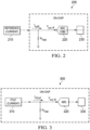
- FIG. 2 illustrates an embodiment of a circuit 200 for storing resistance variation, according to embodiments of the present disclosure. Operation of circuit 200 may be performed during production or production test. Circuit 200 may be operated both before and after packaging to encapsulate chip 120. Chip 200 may implement a portion of chip 120.
- Circuit 200 may include a current source 210 configured to generate a reference current to the chip, though any suitable power source may be used.
- Current source 210 may be configured to send a current output Iout2 so that a resistor of actual resistance RTEST (i.e., the resistor 150 of FIG. 1 ) will generates a voltage Vout_R at an ADC 220.
- ADC 220 may be configured to produce a digital code encoding ADC 220 input (as described above), and to store the digital code in flash memory or another storage 230.
- Storage 230 and ADC 220 may implement the storage and ADC of Fig. 1 , or may be implemented in a similar manner as the storage and ADC of Fig. 1 .
- a first digital code M1 may be generated in circuit 200 and stored in storage 230 prior to wafer packaging.
- a second digital code M2 may be generated in circuit 200 and stored in storage 230 after wafer packaging.
- a package stress ratio ⁇ 1 may be calculated by dividing M1 by M2, or vice versa.
- a system implementing circuit 100 of FIG. 1 may use ⁇ 1 to compensate for package stress on the resistor therein when determining the frequency shift of the voltage output caused by package stress.
- the circuit 200 of FIG. 2 may be combined with the circuit 100 of FIG. 1 .
- the circuit 200 of FIG. 2 may use part of the circuitry on the chip 120 in FIG. 1 to generate two additional digital codes M1 and M2 encoding the pre-package and post-package resistance values of a resistor (e.g., resistor 150).
- a system implementing circuit 100 may, during run-time application to evaluate frequencies of DUT 124, multiply the voltage output (whether as input to or output from ADC 128) times the package stress ratio ⁇ 1.
- the package stress ratio ⁇ 1 may thus be determined during production, while calculated from two such stages during production.
- FIG. 3 is a third block diagram illustrating an additional or alternative circuit 300 to circuit 200 of FIG. 2 , according to embodiments of the present disclosure.
- Circuit 300 may be configured to measure the voltage slope of the temperature variation using a current source 310 that experiences a proportional to absolute temperature (PTAT) variation of the current.
- PTAT variation may describe the degree to which performance may change while temperature changes.
- Circuit 300 may include a current source 310.
- Current source 310 may be a PTAT current source disposed inside the chip that includes an oscillator.
- the PTAT current source may include one or more circuit components using complementary metal-oxide-semiconductor (CMOS). That is, the output current IPTAT of current source 310 may change linearly over a temperature range.
- CMOS complementary metal-oxide-semiconductor
- the variable current IPTAT causes the resistor RTEST to bear a voltage VouT_R so that ADC 320 generates different digital codes for different temperatures, storing generated codes in flash
- circuit 300 may be configured to store a digital code M3 that indicates the voltage of IPTAT applied on RTEST at a first temperature.
- Circuit 300 may be configured to store a fourth digital code M4 that indicates the voltage of IPTAT applied on RTEST at a second temperature.
- the system may calculate a PTAT ratio ⁇ 2 by dividing M3 by M4 or vice-versa.
- the system may later, by an end user, use the PTAT ratio ⁇ 2 to compensate the frequency shift in RC-oscillator caused by temperature changes.
- a system implementing circuit 100 may, during run-time application to evaluate frequencies of DUT 124, multiply the voltage output (whether as input to or output from ADC 128) times the PTAT ratio ⁇ 2.
- the PTAT slope ratio ⁇ 2 may thus be determined during production, while calculated from two such stages during production.
- the ratio ⁇ 2 may be used when, in application of circuit 100, the temperature reaches the temperature used to find M4.
- the temperature at which M3 was determined may have been the temperature at which codes were stored for circuit 100.
- applying the ratio ⁇ 2 to a voltage yielded from a tested frequency may factor in a change in temperature reflected by the differences of temperatures used to find M3 and M4.
- Multiple instances of ⁇ 2 may be tested and stored, wherein different possible temperatures at which circuit 100 is used during applications may be stored via memory codes corresponding to the different changes.
- a system implementing circuit 100 may, during run-time application to evaluate frequencies of DUT 124, multiply the voltage output (whether as input to or output from ADC 128) times the ratio ⁇ 2.
- circuit 300 may be executed once with a PTAT corresponding to 25° C.
- the resulting code may be stored in storage as M3.
- Circuit 300 may be executed subsequently with a PTAT corresponding to 85° C.
- the resulting code may be stored in storage as M4.
- FIG. 4 is a block diagram illustrating a circuit 400 for on-the-fly frequency correction of an oscillator in a deployed chip, according to embodiments of the present disclosure.
- Circuit 400 may implement circuit 100.
- circuit 400 may be the same as circuit 100, but in a post-production deployed chip.
- Circuit 400 may include or be coupled to a frequency source 410 that generates a reference frequency to a mux 422.
- frequency source 410 might be omitted or not used in particular circumstances. In such a case, such an input to mux 422 might be ignored and the other input used.
- a DUT 430 may provide a frequency input to the mux 422.
- Circuit 400 may include a storage 424 that stores the one or more digital codes disclosed above.
- ADC 426 may be configured to covert the voltage signal Vout_freq applied on RTEST to a digital code, as described above.
- Circuit 400 may operate similarly to circuit 100 of FIG. 1 .
- Circuit 400 may include a calculation engine 428.
- Calculation engine 428 may be implemented with digital circuitry, analog circuitry, or circuitry for executing instructions by a processor, or any combination thereof.
- Calculation engine 428 may be configured to accept as input a present value of DUT 430 frequency.
- calculation engine 428 may be configured to accept as input a reference value of a frequency stored in storage 424 that represents the digital code of a known reference frequency previously stored.
- Such a digital code may include the code of the reference frequency source in FIG. 1 and stored during production or production test.
- calculation engine 428 may also accept ratios ⁇ 1 or ⁇ 2 to account for stress changes or temperature changes. These may have been stored in storage 424 as well.
- Calculation engine 428 may be configured to provide a feedback correction signal to DUT 430 based upon its inputs.
- the feedback correction signal may include trimming or trim bits.
- a controller for DUT 430 may accept trim bits that may adjust the frequency of DUT 430 up or down according to an amount based upon an available number of bits. The number of trimming bits may vary according to the implementation of DUT 430.
- Calculation engine 428 may adjust the feedback correction signal to DUT 430 iteratively.
- the iterative process of changing the frequency of DUT 430, measuring the next differential between the a digital code of the reference frequency and a digital code of the actual frequency of DUT 430, and making a subsequent change to the frequency of DUT 430 may be performed in any suitable way.
- the iterative process may mirror that of a binary search, heap search, bubble search, or other suitable algorithm.
- An initial measurement of the differential frequency may be evaluated and the frequency may be adjusted according to half of the range of possible trimming between the present value and a maximum or minimum value.
- a subsequent measurement of the differential frequency may be evaluated and the frequency may be adjusted according to half of the range of possible trimming between the present value and a minimum/maximum value and the previous value.
- Calculation engine 428 may iterate adjustments for a fixed number of cycles, until a minimum error is met, continuously, or any other suitable criteria.
- Circuit 400 may thus correct frequency on-the fly by using the frequency locking loop that compares the reference information and the OUT information and outputs a correction signal containing instructions for the DUT 430 to correct for the difference between the two codes.
- the frequency is determined to be correct.
- Circuit 400 may be operated in use cases such as end users to provide just-in-time or on-the-fly trimming during operation.
- the frequency used to power the SC circuit may be the changing, variable frequency of DUT 430.
- Circuit 100 may be operated in use cases such as production or production test.
- the frequency used to power the SC circuit may be the known, set reference frequency that is stored.
- a system that operates its circuits according to FIGS. 1-4 for trimming may successfully implement on-the-fly trimming.
- Such a system may overcome the lack of a reliable, known reference frequency that matches that frequency used in production or production test.
- the system may take into account package stresses that would otherwise change the frequency response of the system components such as a DUT.
- ratio ⁇ 2 the system may take into account temperature response changes that would otherwise change the frequency response of the system components.
- the system can perform efficiently depending upon the necessary context.
- the long amount of time to start up a DUT, wait for an oscillator to warm up or settle, or wait for other elements (such as memory or processors of a microcontroller including the oscillator or DUT) may be expensive when aggregated together. Accordingly, during production or production test, the response of the DUT might not be used and instead the reference frequency applied and the resulting digital code stored.
- the several milliseconds needed to start up a DUT, wait for an oscillator to warm up or settle, or wait for other elements (such as memory or processors of a microcontroller including the oscillator or DUT) may be acceptable given that a single such DUT needs to come online. Testing of DUT and making subsequent adjustments over even thousands of cycles may be acceptable within the use case of the end user, who might need to only trim a limited number of such DUTs.
- the digital code that is stored is applicable to the same SC network when evaluating any other frequency source that is supposed to be of the same frequency. For example, an 8 MHz source will produce a digital code M0. Later, M0 may be used to validate and trim a real-world DUT that is supposed to have a frequency of 8 Mhz by using M0 on the same SC network, ADC, and RTEST.
- the system that operates its circuits according to FIGS. 1-4 may experience performance advantages over other systems.
- a DUT test at 25° C, correcting to a known frequency. This may take as long as 8 ms, including several thousand cycles for the DUT to settle.
- the DUT test may be repeated for 85° C, correcting to the known frequency. This may also take as long as 8 ms.
- the DUT test After packaging, at 25° C, the DUT test may be repeated, correcting to the known frequency. This trim steps may require that, during production or production test, the tester has to wait for oscillator to start and become stable.
- the system that operates its circuits according to FIGS. 1-4 may overcome problems of such a long wake-up and settling time for RC oscillators.
- the system might not run a DUT test during production or production test and thus not wait for RC oscillators to settle. Instead, the system may store the digital codes of the particular SC network, ADC, and RTEST. Before packaging, at 25° C, the voltage value may be measured and stored for the known reference frequency source. This may be repeated at 85° C. The ratio of the two may define a frequency shift due to temperature. This may be repeated with the voltage from PTAT current sources to get PTAT correction information. After packaging, the digital code of the reference frequency source may be stored again to account for changes in frequency response caused by stresses of packaging. These may be accomplished in as short of a time as 80 microseconds
- FIG. 5 is an example flow chart illustrating a method 500 for oscillator trimming, according to embodiments of the present disclosure.
- the circuit system measures and stores a first product of current and resistor values at a first temperature.
- the first temperature may, for example, be 25° C ⁇
- the circuit system measures and stores a second product of current and resistor values at a second temperature.
- the second temperature may, for example, be 85° C or another temperature that is different from the first temperature.
- the circuit system may calculate a ratio that gives the frequency shift in fosc due to temperature.
- the circuit system may repeat steps 510 and 520 with a variable current input IPTAT to get PTAT correction information such as the PTAT ratio n2.
- the circuit system measures and stores a digital code for the desired frequency Fref.
- the circuit system may obtain the digital code for the desired frequency Fref at 25 C° before the oscillator is installed or packaged.
- step 540 the circuit system measures and stores a digital code corresponding to the product of Iout and RTEST. After the oscillator is packaged, the circuit system obtains a second digital code corresponding to the product of lout and RTEST at25° C ⁇
- the circuit system calculates the package stress ratio and correct the package stress ratio in trim-codes. For example, the circuit system may correct the frequency of the DUT output by using the stored digital codes and the corrected package stress ratio.
- the circuit system may iteratively measure the frequency of an oscillator under test and adjust or trim the frequency based upon differences between the oscillator and known values stored from the steps above. Furthermore, the oscillator frequency may be adjusted based upon temperature and stress ratios.
- the system may measure two voltage signals when IPTAT is input to the IPTAT into RTEST (such as in FIGURE 3 ) at two different temperatures.
- the circuit system may obtain the PTAT correction information accordingly.
- the proposed integrated circuit may be used for automotive safety applications when it is essential to meet the requirements of stability and avoid over driving the crystal. Further, the proposed integrated circuit may be used across multiple computing device divisions and/or platforms, including without limitation: 16- bit and/or 32-bit microcontrollers; portable device platforms such as Windows Portable Devices (WPD) and/or Wearable Smart Gateway; and the like.
- WPD Windows Portable Devices
- Method 400 may begin at any suitable point, such as at step 402.
- Method 500 may be implemented as instructions for execution by a processor that are embodied in one or more computer-readable media such as a memory.
- the instructions when loaded and executed by the processor, may cause the microcontroller or processor to implement the functionality of the present disclosure.
- Method 500 may begin at any suitable point, such as at step 510.
- Method 500 may be implemented as instructions for execution by a processor that are embodied in one or more computer-readable media such as a memory.
- the instructions when loaded and executed by the processor, may cause the microcontroller or processor to implement the functionality of the present disclosure.
- Method 500 may be implemented by any suitable mechanism, such as the elements of FIGURES 1-4 .
Landscapes
- Engineering & Computer Science (AREA)
- General Engineering & Computer Science (AREA)
- Physics & Mathematics (AREA)
- General Physics & Mathematics (AREA)
- Semiconductor Integrated Circuits (AREA)
- Tests Of Electronic Circuits (AREA)
- Oscillators With Electromechanical Resonators (AREA)
- Inductance-Capacitance Distribution Constants And Capacitance-Resistance Oscillators (AREA)
Applications Claiming Priority (3)
| Application Number | Priority Date | Filing Date | Title |
|---|---|---|---|
| US201662379632P | 2016-08-25 | 2016-08-25 | |
| US15/685,570 US10551428B2 (en) | 2016-08-25 | 2017-08-24 | Systems and methods for storing frequency information for system calibration/trimming |
| PCT/US2017/048574 WO2018039538A1 (en) | 2016-08-25 | 2017-08-25 | Systems and methods for storing frequency information for system calibration and trimming |
Publications (2)
| Publication Number | Publication Date |
|---|---|
| EP3504798A1 EP3504798A1 (en) | 2019-07-03 |
| EP3504798B1 true EP3504798B1 (en) | 2023-04-05 |
Family
ID=61242213
Family Applications (1)
| Application Number | Title | Priority Date | Filing Date |
|---|---|---|---|
| EP17764717.9A Active EP3504798B1 (en) | 2016-08-25 | 2017-08-25 | Systems and methods for storing frequency information for system calibration and trimming |
Country Status (7)
| Country | Link |
|---|---|
| US (1) | US10551428B2 (https=) |
| EP (1) | EP3504798B1 (https=) |
| JP (1) | JP6978437B2 (https=) |
| KR (1) | KR102458148B1 (https=) |
| CN (1) | CN109314517A (https=) |
| TW (1) | TW201813313A (https=) |
| WO (1) | WO2018039538A1 (https=) |
Families Citing this family (2)
| Publication number | Priority date | Publication date | Assignee | Title |
|---|---|---|---|---|
| US10866269B2 (en) * | 2017-11-16 | 2020-12-15 | Microchip Technology Incorporated | Fast frequency calculator |
| CN114421890A (zh) * | 2022-01-21 | 2022-04-29 | 南京扬贺扬微电子科技有限公司 | 一种优化校正的rc振荡模块及方法 |
Citations (1)
| Publication number | Priority date | Publication date | Assignee | Title |
|---|---|---|---|---|
| US20150249453A1 (en) * | 2014-02-28 | 2015-09-03 | Texas Instruments Incorporated | Fast on-chip oscillator trimming |
Family Cites Families (14)
| Publication number | Priority date | Publication date | Assignee | Title |
|---|---|---|---|---|
| US5796312A (en) * | 1996-05-24 | 1998-08-18 | Microchip Technology Incorporated | Microcontroller with firmware selectable oscillator trimming |
| US6813529B2 (en) * | 2001-01-19 | 2004-11-02 | Microchip Technology Incorporated | Method and apparatus for signal frequency decoding without an analog bandpass filter |
| US7541878B2 (en) * | 2005-12-29 | 2009-06-02 | Intel Corporation | Temperature compensated crystal oscillator |
| US7889013B2 (en) * | 2007-08-28 | 2011-02-15 | Intel Corporation | Microelectronic die having CMOS ring oscillator thereon and method of using same |
| US7737794B2 (en) * | 2008-05-14 | 2010-06-15 | International Business Machines Corporation | Phase locked loop with temperature and process compensation |
| US20100244969A1 (en) * | 2009-03-30 | 2010-09-30 | Mediatek Inc. | Temperature compensated oscillation circuits |
| WO2012001846A1 (ja) * | 2010-06-28 | 2012-01-05 | パナソニック株式会社 | 基準周波数生成回路、半導体集積回路、電子機器 |
| US8451064B2 (en) * | 2010-10-07 | 2013-05-28 | Advanced Micro Devices, Inc. | Voltage-controlled oscillator module having adjustable oscillator gain and related operating methods |
| WO2012137590A1 (ja) | 2011-04-01 | 2012-10-11 | ルネサスエレクトロニクス株式会社 | 半導体装置 |
| US8390384B1 (en) | 2011-11-21 | 2013-03-05 | Microchip Technology Incorporated | Precision on-board tuning of embedded microcontroller oscillator using charge time measurement unit |
| US9236852B2 (en) | 2012-02-01 | 2016-01-12 | Microchip Technology Incorporated | Input capture peripheral with gating logic |
| JP6116305B2 (ja) * | 2013-03-25 | 2017-04-19 | 三菱電機株式会社 | 周波数検出回路 |
| JP2015152416A (ja) * | 2014-02-14 | 2015-08-24 | 株式会社東芝 | キャパシタンス検出装置 |
| DE102015202694A1 (de) * | 2015-02-13 | 2016-08-18 | Infineon Technologies Ag | Stresskompensierte Oszillatorschaltungsanordnung und integrierte Schaltung, die diese verwendet |
-
2017
- 2017-08-24 US US15/685,570 patent/US10551428B2/en not_active Expired - Fee Related
- 2017-08-25 TW TW106128988A patent/TW201813313A/zh unknown
- 2017-08-25 WO PCT/US2017/048574 patent/WO2018039538A1/en not_active Ceased
- 2017-08-25 EP EP17764717.9A patent/EP3504798B1/en active Active
- 2017-08-25 JP JP2018560005A patent/JP6978437B2/ja not_active Expired - Fee Related
- 2017-08-25 CN CN201780026137.6A patent/CN109314517A/zh active Pending
- 2017-08-25 KR KR1020187031999A patent/KR102458148B1/ko active Active
Patent Citations (1)
| Publication number | Priority date | Publication date | Assignee | Title |
|---|---|---|---|---|
| US20150249453A1 (en) * | 2014-02-28 | 2015-09-03 | Texas Instruments Incorporated | Fast on-chip oscillator trimming |
Also Published As
| Publication number | Publication date |
|---|---|
| WO2018039538A1 (en) | 2018-03-01 |
| TW201813313A (zh) | 2018-04-01 |
| US10551428B2 (en) | 2020-02-04 |
| CN109314517A (zh) | 2019-02-05 |
| JP6978437B2 (ja) | 2021-12-08 |
| JP2019533318A (ja) | 2019-11-14 |
| KR102458148B1 (ko) | 2022-10-25 |
| EP3504798A1 (en) | 2019-07-03 |
| KR20190040482A (ko) | 2019-04-18 |
| US20180059171A1 (en) | 2018-03-01 |
Similar Documents
| Publication | Publication Date | Title |
|---|---|---|
| US10250266B2 (en) | Oscillator calibration system | |
| US7209013B2 (en) | Systems and methods for self-calibration | |
| US8330446B2 (en) | Calibration apparatus and calibration method thereof | |
| CN106817080B (zh) | 电路装置、振荡器、电子设备、移动体及振荡器的制造方法 | |
| CN107896105B (zh) | 用于锁相回路的片上测量 | |
| US20130002274A1 (en) | Aging degradation diagnosis circuit and aging degradation diagnosis method for semiconductor integrated circuit | |
| US11500336B1 (en) | Methods and apparatus for low jitter fractional output dividers | |
| US10763832B2 (en) | Precision oscillators that use imprecise components | |
| EP3504798B1 (en) | Systems and methods for storing frequency information for system calibration and trimming | |
| TW201535979A (zh) | 主時脈高精度振盪器 | |
| US20050110513A1 (en) | Semiconductor test module and method of testing semiconductor device | |
| CN110880933B (zh) | 具有一半步级解析度的片载校正电路及方法 | |
| US20180006654A1 (en) | Simultaneous multi-effect oscillator compensation using piecewise interdependent polynomials | |
| US9502956B1 (en) | Configuration of semiconductor device supply voltage | |
| KR20210081583A (ko) | 컴포넌트에 대한 트리밍 기능을 갖는 집적 회로 | |
| CN114041091B (zh) | 用于tdc的电源电路模块和所述电源电路模块的校准方法 | |
| KR100836530B1 (ko) | 보정가능한 온칩 발진 회로 | |
| JP7429114B2 (ja) | デジタル制御発振器を備える半導体デバイスおよびその試験方法 | |
| US7498891B2 (en) | Method for calibration of an oscillator for a microcontroller chip operation | |
| CN115756069B (zh) | 一种免片外晶振的高精度低温漂驰张振荡器及校准方法 | |
| WO2001033249A2 (en) | Radio calibration by correcting the crystal oscillator frequency | |
| Banerjee et al. | A Machine Learning Based Built-In Self-Test Method for Lifetime Frequency Drift Compensation of Precision Oscillators | |
| CN117639740A (zh) | 延时监测电路 | |
| Roshan | A MEMS-assisted Dual-resonator Temperature-to-digital Converter |
Legal Events
| Date | Code | Title | Description |
|---|---|---|---|
| STAA | Information on the status of an ep patent application or granted ep patent |
Free format text: STATUS: UNKNOWN |
|
| STAA | Information on the status of an ep patent application or granted ep patent |
Free format text: STATUS: THE INTERNATIONAL PUBLICATION HAS BEEN MADE |
|
| PUAI | Public reference made under article 153(3) epc to a published international application that has entered the european phase |
Free format text: ORIGINAL CODE: 0009012 |
|
| STAA | Information on the status of an ep patent application or granted ep patent |
Free format text: STATUS: REQUEST FOR EXAMINATION WAS MADE |
|
| 17P | Request for examination filed |
Effective date: 20190322 |
|
| AK | Designated contracting states |
Kind code of ref document: A1 Designated state(s): AL AT BE BG CH CY CZ DE DK EE ES FI FR GB GR HR HU IE IS IT LI LT LU LV MC MK MT NL NO PL PT RO RS SE SI SK SM TR |
|
| AX | Request for extension of the european patent |
Extension state: BA ME |
|
| DAV | Request for validation of the european patent (deleted) | ||
| DAX | Request for extension of the european patent (deleted) | ||
| STAA | Information on the status of an ep patent application or granted ep patent |
Free format text: STATUS: EXAMINATION IS IN PROGRESS |
|
| 17Q | First examination report despatched |
Effective date: 20210514 |
|
| GRAP | Despatch of communication of intention to grant a patent |
Free format text: ORIGINAL CODE: EPIDOSNIGR1 |
|
| STAA | Information on the status of an ep patent application or granted ep patent |
Free format text: STATUS: GRANT OF PATENT IS INTENDED |
|
| RIC1 | Information provided on ipc code assigned before grant |
Ipc: G01R 31/28 20060101ALI20220921BHEP Ipc: H03L 1/02 20060101ALI20220921BHEP Ipc: H03L 7/02 20060101ALI20220921BHEP Ipc: H03L 1/00 20060101AFI20220921BHEP |
|
| INTG | Intention to grant announced |
Effective date: 20221021 |
|
| GRAS | Grant fee paid |
Free format text: ORIGINAL CODE: EPIDOSNIGR3 |
|
| GRAA | (expected) grant |
Free format text: ORIGINAL CODE: 0009210 |
|
| STAA | Information on the status of an ep patent application or granted ep patent |
Free format text: STATUS: THE PATENT HAS BEEN GRANTED |
|
| AK | Designated contracting states |
Kind code of ref document: B1 Designated state(s): AL AT BE BG CH CY CZ DE DK EE ES FI FR GB GR HR HU IE IS IT LI LT LU LV MC MK MT NL NO PL PT RO RS SE SI SK SM TR |
|
| REG | Reference to a national code |
Ref country code: GB Ref legal event code: FG4D |
|
| REG | Reference to a national code |
Ref country code: DE Ref legal event code: R096 Ref document number: 602017067465 Country of ref document: DE |
|
| REG | Reference to a national code |
Ref country code: CH Ref legal event code: EP |
|
| REG | Reference to a national code |
Ref country code: AT Ref legal event code: REF Ref document number: 1559022 Country of ref document: AT Kind code of ref document: T Effective date: 20230415 |
|
| REG | Reference to a national code |
Ref country code: IE Ref legal event code: FG4D |
|
| REG | Reference to a national code |
Ref country code: LT Ref legal event code: MG9D |
|
| REG | Reference to a national code |
Ref country code: NL Ref legal event code: MP Effective date: 20230405 |
|
| REG | Reference to a national code |
Ref country code: AT Ref legal event code: MK05 Ref document number: 1559022 Country of ref document: AT Kind code of ref document: T Effective date: 20230405 |
|
| PG25 | Lapsed in a contracting state [announced via postgrant information from national office to epo] |
Ref country code: NL Free format text: LAPSE BECAUSE OF FAILURE TO SUBMIT A TRANSLATION OF THE DESCRIPTION OR TO PAY THE FEE WITHIN THE PRESCRIBED TIME-LIMIT Effective date: 20230405 |
|
| PG25 | Lapsed in a contracting state [announced via postgrant information from national office to epo] |
Ref country code: SE Free format text: LAPSE BECAUSE OF FAILURE TO SUBMIT A TRANSLATION OF THE DESCRIPTION OR TO PAY THE FEE WITHIN THE PRESCRIBED TIME-LIMIT Effective date: 20230405 Ref country code: PT Free format text: LAPSE BECAUSE OF FAILURE TO SUBMIT A TRANSLATION OF THE DESCRIPTION OR TO PAY THE FEE WITHIN THE PRESCRIBED TIME-LIMIT Effective date: 20230807 Ref country code: NO Free format text: LAPSE BECAUSE OF FAILURE TO SUBMIT A TRANSLATION OF THE DESCRIPTION OR TO PAY THE FEE WITHIN THE PRESCRIBED TIME-LIMIT Effective date: 20230705 Ref country code: ES Free format text: LAPSE BECAUSE OF FAILURE TO SUBMIT A TRANSLATION OF THE DESCRIPTION OR TO PAY THE FEE WITHIN THE PRESCRIBED TIME-LIMIT Effective date: 20230405 Ref country code: AT Free format text: LAPSE BECAUSE OF FAILURE TO SUBMIT A TRANSLATION OF THE DESCRIPTION OR TO PAY THE FEE WITHIN THE PRESCRIBED TIME-LIMIT Effective date: 20230405 |
|
| PG25 | Lapsed in a contracting state [announced via postgrant information from national office to epo] |
Ref country code: RS Free format text: LAPSE BECAUSE OF FAILURE TO SUBMIT A TRANSLATION OF THE DESCRIPTION OR TO PAY THE FEE WITHIN THE PRESCRIBED TIME-LIMIT Effective date: 20230405 Ref country code: PL Free format text: LAPSE BECAUSE OF FAILURE TO SUBMIT A TRANSLATION OF THE DESCRIPTION OR TO PAY THE FEE WITHIN THE PRESCRIBED TIME-LIMIT Effective date: 20230405 Ref country code: LV Free format text: LAPSE BECAUSE OF FAILURE TO SUBMIT A TRANSLATION OF THE DESCRIPTION OR TO PAY THE FEE WITHIN THE PRESCRIBED TIME-LIMIT Effective date: 20230405 Ref country code: LT Free format text: LAPSE BECAUSE OF FAILURE TO SUBMIT A TRANSLATION OF THE DESCRIPTION OR TO PAY THE FEE WITHIN THE PRESCRIBED TIME-LIMIT Effective date: 20230405 Ref country code: IS Free format text: LAPSE BECAUSE OF FAILURE TO SUBMIT A TRANSLATION OF THE DESCRIPTION OR TO PAY THE FEE WITHIN THE PRESCRIBED TIME-LIMIT Effective date: 20230805 Ref country code: HR Free format text: LAPSE BECAUSE OF FAILURE TO SUBMIT A TRANSLATION OF THE DESCRIPTION OR TO PAY THE FEE WITHIN THE PRESCRIBED TIME-LIMIT Effective date: 20230405 Ref country code: GR Free format text: LAPSE BECAUSE OF FAILURE TO SUBMIT A TRANSLATION OF THE DESCRIPTION OR TO PAY THE FEE WITHIN THE PRESCRIBED TIME-LIMIT Effective date: 20230706 Ref country code: AL Free format text: LAPSE BECAUSE OF FAILURE TO SUBMIT A TRANSLATION OF THE DESCRIPTION OR TO PAY THE FEE WITHIN THE PRESCRIBED TIME-LIMIT Effective date: 20230405 |
|
| PG25 | Lapsed in a contracting state [announced via postgrant information from national office to epo] |
Ref country code: FI Free format text: LAPSE BECAUSE OF FAILURE TO SUBMIT A TRANSLATION OF THE DESCRIPTION OR TO PAY THE FEE WITHIN THE PRESCRIBED TIME-LIMIT Effective date: 20230405 |
|
| REG | Reference to a national code |
Ref country code: DE Ref legal event code: R097 Ref document number: 602017067465 Country of ref document: DE |
|
| PG25 | Lapsed in a contracting state [announced via postgrant information from national office to epo] |
Ref country code: SK Free format text: LAPSE BECAUSE OF FAILURE TO SUBMIT A TRANSLATION OF THE DESCRIPTION OR TO PAY THE FEE WITHIN THE PRESCRIBED TIME-LIMIT Effective date: 20230405 |
|
| PG25 | Lapsed in a contracting state [announced via postgrant information from national office to epo] |
Ref country code: SM Free format text: LAPSE BECAUSE OF FAILURE TO SUBMIT A TRANSLATION OF THE DESCRIPTION OR TO PAY THE FEE WITHIN THE PRESCRIBED TIME-LIMIT Effective date: 20230405 Ref country code: SK Free format text: LAPSE BECAUSE OF FAILURE TO SUBMIT A TRANSLATION OF THE DESCRIPTION OR TO PAY THE FEE WITHIN THE PRESCRIBED TIME-LIMIT Effective date: 20230405 Ref country code: RO Free format text: LAPSE BECAUSE OF FAILURE TO SUBMIT A TRANSLATION OF THE DESCRIPTION OR TO PAY THE FEE WITHIN THE PRESCRIBED TIME-LIMIT Effective date: 20230405 Ref country code: EE Free format text: LAPSE BECAUSE OF FAILURE TO SUBMIT A TRANSLATION OF THE DESCRIPTION OR TO PAY THE FEE WITHIN THE PRESCRIBED TIME-LIMIT Effective date: 20230405 Ref country code: DK Free format text: LAPSE BECAUSE OF FAILURE TO SUBMIT A TRANSLATION OF THE DESCRIPTION OR TO PAY THE FEE WITHIN THE PRESCRIBED TIME-LIMIT Effective date: 20230405 Ref country code: CZ Free format text: LAPSE BECAUSE OF FAILURE TO SUBMIT A TRANSLATION OF THE DESCRIPTION OR TO PAY THE FEE WITHIN THE PRESCRIBED TIME-LIMIT Effective date: 20230405 |
|
| PLBE | No opposition filed within time limit |
Free format text: ORIGINAL CODE: 0009261 |
|
| STAA | Information on the status of an ep patent application or granted ep patent |
Free format text: STATUS: NO OPPOSITION FILED WITHIN TIME LIMIT |
|
| REG | Reference to a national code |
Ref country code: DE Ref legal event code: R119 Ref document number: 602017067465 Country of ref document: DE |
|
| PG25 | Lapsed in a contracting state [announced via postgrant information from national office to epo] |
Ref country code: MC Free format text: LAPSE BECAUSE OF FAILURE TO SUBMIT A TRANSLATION OF THE DESCRIPTION OR TO PAY THE FEE WITHIN THE PRESCRIBED TIME-LIMIT Effective date: 20230405 |
|
| 26N | No opposition filed |
Effective date: 20240108 |
|
| REG | Reference to a national code |
Ref country code: CH Ref legal event code: PL |
|
| PG25 | Lapsed in a contracting state [announced via postgrant information from national office to epo] |
Ref country code: MC Free format text: LAPSE BECAUSE OF FAILURE TO SUBMIT A TRANSLATION OF THE DESCRIPTION OR TO PAY THE FEE WITHIN THE PRESCRIBED TIME-LIMIT Effective date: 20230405 |
|
| PG25 | Lapsed in a contracting state [announced via postgrant information from national office to epo] |
Ref country code: LU Free format text: LAPSE BECAUSE OF NON-PAYMENT OF DUE FEES Effective date: 20230825 |
|
| GBPC | Gb: european patent ceased through non-payment of renewal fee |
Effective date: 20230825 |
|
| PG25 | Lapsed in a contracting state [announced via postgrant information from national office to epo] |
Ref country code: LU Free format text: LAPSE BECAUSE OF NON-PAYMENT OF DUE FEES Effective date: 20230825 Ref country code: CH Free format text: LAPSE BECAUSE OF NON-PAYMENT OF DUE FEES Effective date: 20230831 |
|
| PG25 | Lapsed in a contracting state [announced via postgrant information from national office to epo] |
Ref country code: SI Free format text: LAPSE BECAUSE OF FAILURE TO SUBMIT A TRANSLATION OF THE DESCRIPTION OR TO PAY THE FEE WITHIN THE PRESCRIBED TIME-LIMIT Effective date: 20230405 |
|
| REG | Reference to a national code |
Ref country code: BE Ref legal event code: MM Effective date: 20230831 |
|
| REG | Reference to a national code |
Ref country code: IE Ref legal event code: MM4A |
|
| PG25 | Lapsed in a contracting state [announced via postgrant information from national office to epo] |
Ref country code: SI Free format text: LAPSE BECAUSE OF FAILURE TO SUBMIT A TRANSLATION OF THE DESCRIPTION OR TO PAY THE FEE WITHIN THE PRESCRIBED TIME-LIMIT Effective date: 20230405 Ref country code: IT Free format text: LAPSE BECAUSE OF FAILURE TO SUBMIT A TRANSLATION OF THE DESCRIPTION OR TO PAY THE FEE WITHIN THE PRESCRIBED TIME-LIMIT Effective date: 20230405 |
|
| PG25 | Lapsed in a contracting state [announced via postgrant information from national office to epo] |
Ref country code: IE Free format text: LAPSE BECAUSE OF NON-PAYMENT OF DUE FEES Effective date: 20230825 |
|
| PG25 | Lapsed in a contracting state [announced via postgrant information from national office to epo] |
Ref country code: GB Free format text: LAPSE BECAUSE OF NON-PAYMENT OF DUE FEES Effective date: 20230825 |
|
| PG25 | Lapsed in a contracting state [announced via postgrant information from national office to epo] |
Ref country code: IE Free format text: LAPSE BECAUSE OF NON-PAYMENT OF DUE FEES Effective date: 20230825 Ref country code: GB Free format text: LAPSE BECAUSE OF NON-PAYMENT OF DUE FEES Effective date: 20230825 Ref country code: FR Free format text: LAPSE BECAUSE OF NON-PAYMENT OF DUE FEES Effective date: 20230831 Ref country code: DE Free format text: LAPSE BECAUSE OF NON-PAYMENT OF DUE FEES Effective date: 20240301 |
|
| PG25 | Lapsed in a contracting state [announced via postgrant information from national office to epo] |
Ref country code: BE Free format text: LAPSE BECAUSE OF NON-PAYMENT OF DUE FEES Effective date: 20230831 |
|
| PG25 | Lapsed in a contracting state [announced via postgrant information from national office to epo] |
Ref country code: BG Free format text: LAPSE BECAUSE OF FAILURE TO SUBMIT A TRANSLATION OF THE DESCRIPTION OR TO PAY THE FEE WITHIN THE PRESCRIBED TIME-LIMIT Effective date: 20230405 |
|
| PG25 | Lapsed in a contracting state [announced via postgrant information from national office to epo] |
Ref country code: BG Free format text: LAPSE BECAUSE OF FAILURE TO SUBMIT A TRANSLATION OF THE DESCRIPTION OR TO PAY THE FEE WITHIN THE PRESCRIBED TIME-LIMIT Effective date: 20230405 |
|
| PG25 | Lapsed in a contracting state [announced via postgrant information from national office to epo] |
Ref country code: CY Free format text: LAPSE BECAUSE OF FAILURE TO SUBMIT A TRANSLATION OF THE DESCRIPTION OR TO PAY THE FEE WITHIN THE PRESCRIBED TIME-LIMIT; INVALID AB INITIO Effective date: 20170825 |
|
| PG25 | Lapsed in a contracting state [announced via postgrant information from national office to epo] |
Ref country code: HU Free format text: LAPSE BECAUSE OF FAILURE TO SUBMIT A TRANSLATION OF THE DESCRIPTION OR TO PAY THE FEE WITHIN THE PRESCRIBED TIME-LIMIT; INVALID AB INITIO Effective date: 20170825 |
|
| PG25 | Lapsed in a contracting state [announced via postgrant information from national office to epo] |
Ref country code: TR Free format text: LAPSE BECAUSE OF FAILURE TO SUBMIT A TRANSLATION OF THE DESCRIPTION OR TO PAY THE FEE WITHIN THE PRESCRIBED TIME-LIMIT Effective date: 20230405 |