EP3489572A1 - Illumination apparatus having a plurality of semiconductor light-emitting devices - Google Patents
Illumination apparatus having a plurality of semiconductor light-emitting devices Download PDFInfo
- Publication number
- EP3489572A1 EP3489572A1 EP18212110.3A EP18212110A EP3489572A1 EP 3489572 A1 EP3489572 A1 EP 3489572A1 EP 18212110 A EP18212110 A EP 18212110A EP 3489572 A1 EP3489572 A1 EP 3489572A1
- Authority
- EP
- European Patent Office
- Prior art keywords
- light
- semiconductor light
- emitting devices
- reflective layer
- illumination apparatus
- Prior art date
- Legal status (The legal status is an assumption and is not a legal conclusion. Google has not performed a legal analysis and makes no representation as to the accuracy of the status listed.)
- Withdrawn
Links
Images


Classifications
-
- F—MECHANICAL ENGINEERING; LIGHTING; HEATING; WEAPONS; BLASTING
- F21—LIGHTING
- F21V—FUNCTIONAL FEATURES OR DETAILS OF LIGHTING DEVICES OR SYSTEMS THEREOF; STRUCTURAL COMBINATIONS OF LIGHTING DEVICES WITH OTHER ARTICLES, NOT OTHERWISE PROVIDED FOR
- F21V31/00—Gas-tight or water-tight arrangements
- F21V31/04—Provision of filling media
-
- F—MECHANICAL ENGINEERING; LIGHTING; HEATING; WEAPONS; BLASTING
- F21—LIGHTING
- F21K—NON-ELECTRIC LIGHT SOURCES USING LUMINESCENCE; LIGHT SOURCES USING ELECTROCHEMILUMINESCENCE; LIGHT SOURCES USING CHARGES OF COMBUSTIBLE MATERIAL; LIGHT SOURCES USING SEMICONDUCTOR DEVICES AS LIGHT-GENERATING ELEMENTS; LIGHT SOURCES NOT OTHERWISE PROVIDED FOR
- F21K9/00—Light sources using semiconductor devices as light-generating elements, e.g. using light-emitting diodes [LED] or lasers
- F21K9/60—Optical arrangements integrated in the light source, e.g. for improving the colour rendering index or the light extraction
- F21K9/68—Details of reflectors forming part of the light source
-
- H—ELECTRICITY
- H01—ELECTRIC ELEMENTS
- H01L—SEMICONDUCTOR DEVICES NOT COVERED BY CLASS H10
- H01L25/00—Assemblies consisting of a plurality of individual semiconductor or other solid state devices ; Multistep manufacturing processes thereof
- H01L25/03—Assemblies consisting of a plurality of individual semiconductor or other solid state devices ; Multistep manufacturing processes thereof all the devices being of a type provided for in the same subgroup of groups H01L27/00 - H01L33/00, or in a single subclass of H10K, H10N, e.g. assemblies of rectifier diodes
- H01L25/04—Assemblies consisting of a plurality of individual semiconductor or other solid state devices ; Multistep manufacturing processes thereof all the devices being of a type provided for in the same subgroup of groups H01L27/00 - H01L33/00, or in a single subclass of H10K, H10N, e.g. assemblies of rectifier diodes the devices not having separate containers
- H01L25/075—Assemblies consisting of a plurality of individual semiconductor or other solid state devices ; Multistep manufacturing processes thereof all the devices being of a type provided for in the same subgroup of groups H01L27/00 - H01L33/00, or in a single subclass of H10K, H10N, e.g. assemblies of rectifier diodes the devices not having separate containers the devices being of a type provided for in group H01L33/00
- H01L25/0753—Assemblies consisting of a plurality of individual semiconductor or other solid state devices ; Multistep manufacturing processes thereof all the devices being of a type provided for in the same subgroup of groups H01L27/00 - H01L33/00, or in a single subclass of H10K, H10N, e.g. assemblies of rectifier diodes the devices not having separate containers the devices being of a type provided for in group H01L33/00 the devices being arranged next to each other
-
- F—MECHANICAL ENGINEERING; LIGHTING; HEATING; WEAPONS; BLASTING
- F21—LIGHTING
- F21Y—INDEXING SCHEME ASSOCIATED WITH SUBCLASSES F21K, F21L, F21S and F21V, RELATING TO THE FORM OR THE KIND OF THE LIGHT SOURCES OR OF THE COLOUR OF THE LIGHT EMITTED
- F21Y2105/00—Planar light sources
- F21Y2105/10—Planar light sources comprising a two-dimensional array of point-like light-generating elements
-
- F—MECHANICAL ENGINEERING; LIGHTING; HEATING; WEAPONS; BLASTING
- F21—LIGHTING
- F21Y—INDEXING SCHEME ASSOCIATED WITH SUBCLASSES F21K, F21L, F21S and F21V, RELATING TO THE FORM OR THE KIND OF THE LIGHT SOURCES OR OF THE COLOUR OF THE LIGHT EMITTED
- F21Y2115/00—Light-generating elements of semiconductor light sources
- F21Y2115/10—Light-emitting diodes [LED]
-
- H—ELECTRICITY
- H01—ELECTRIC ELEMENTS
- H01L—SEMICONDUCTOR DEVICES NOT COVERED BY CLASS H10
- H01L2224/00—Indexing scheme for arrangements for connecting or disconnecting semiconductor or solid-state bodies and methods related thereto as covered by H01L24/00
- H01L2224/01—Means for bonding being attached to, or being formed on, the surface to be connected, e.g. chip-to-package, die-attach, "first-level" interconnects; Manufacturing methods related thereto
- H01L2224/42—Wire connectors; Manufacturing methods related thereto
- H01L2224/47—Structure, shape, material or disposition of the wire connectors after the connecting process
- H01L2224/48—Structure, shape, material or disposition of the wire connectors after the connecting process of an individual wire connector
- H01L2224/4805—Shape
- H01L2224/4809—Loop shape
- H01L2224/48091—Arched
-
- H—ELECTRICITY
- H01—ELECTRIC ELEMENTS
- H01L—SEMICONDUCTOR DEVICES NOT COVERED BY CLASS H10
- H01L2224/00—Indexing scheme for arrangements for connecting or disconnecting semiconductor or solid-state bodies and methods related thereto as covered by H01L24/00
- H01L2224/01—Means for bonding being attached to, or being formed on, the surface to be connected, e.g. chip-to-package, die-attach, "first-level" interconnects; Manufacturing methods related thereto
- H01L2224/42—Wire connectors; Manufacturing methods related thereto
- H01L2224/47—Structure, shape, material or disposition of the wire connectors after the connecting process
- H01L2224/49—Structure, shape, material or disposition of the wire connectors after the connecting process of a plurality of wire connectors
- H01L2224/491—Disposition
- H01L2224/4911—Disposition the connectors being bonded to at least one common bonding area, e.g. daisy chain
-
- H—ELECTRICITY
- H01—ELECTRIC ELEMENTS
- H01L—SEMICONDUCTOR DEVICES NOT COVERED BY CLASS H10
- H01L2224/00—Indexing scheme for arrangements for connecting or disconnecting semiconductor or solid-state bodies and methods related thereto as covered by H01L24/00
- H01L2224/73—Means for bonding being of different types provided for in two or more of groups H01L2224/10, H01L2224/18, H01L2224/26, H01L2224/34, H01L2224/42, H01L2224/50, H01L2224/63, H01L2224/71
- H01L2224/732—Location after the connecting process
- H01L2224/73251—Location after the connecting process on different surfaces
- H01L2224/73265—Layer and wire connectors
-
- H—ELECTRICITY
- H01—ELECTRIC ELEMENTS
- H01L—SEMICONDUCTOR DEVICES NOT COVERED BY CLASS H10
- H01L2924/00—Indexing scheme for arrangements or methods for connecting or disconnecting semiconductor or solid-state bodies as covered by H01L24/00
- H01L2924/19—Details of hybrid assemblies other than the semiconductor or other solid state devices to be connected
- H01L2924/191—Disposition
- H01L2924/19101—Disposition of discrete passive components
- H01L2924/19107—Disposition of discrete passive components off-chip wires
-
- H—ELECTRICITY
- H01—ELECTRIC ELEMENTS
- H01L—SEMICONDUCTOR DEVICES NOT COVERED BY CLASS H10
- H01L33/00—Semiconductor devices with at least one potential-jump barrier or surface barrier specially adapted for light emission; Processes or apparatus specially adapted for the manufacture or treatment thereof or of parts thereof; Details thereof
- H01L33/48—Semiconductor devices with at least one potential-jump barrier or surface barrier specially adapted for light emission; Processes or apparatus specially adapted for the manufacture or treatment thereof or of parts thereof; Details thereof characterised by the semiconductor body packages
- H01L33/58—Optical field-shaping elements
- H01L33/60—Reflective elements
Landscapes
- Engineering & Computer Science (AREA)
- Microelectronics & Electronic Packaging (AREA)
- Power Engineering (AREA)
- Physics & Mathematics (AREA)
- General Engineering & Computer Science (AREA)
- Computer Hardware Design (AREA)
- General Physics & Mathematics (AREA)
- Condensed Matter Physics & Semiconductors (AREA)
- Optics & Photonics (AREA)
- Led Device Packages (AREA)
- Led Devices (AREA)
- Fastening Of Light Sources Or Lamp Holders (AREA)
- Arrangement Of Elements, Cooling, Sealing, Or The Like Of Lighting Devices (AREA)
- Non-Portable Lighting Devices Or Systems Thereof (AREA)
Abstract
Description
- The present invention relates to an illumination apparatus using a plurality of semiconductor light-emitting devices, such as light-emitting diode chips, as a light source thereof.
- Known are LED displays having a plurality of light-emitting diode chips forming a pixel, and a cover member surrounding the light-emitting diode chips.
- The light-emitting diode chips are mounted in a line on a printed wiring board. The cover member has a cavity which contains light-emitting diode chips for one pixel, and a sealing material formed of synthetic resin is filled into the cavity. The light-emitting diode chips for one pixel are molded as one unitary piece with the cover member by the sealing member. For example, Japanese Patent No.
3329573 - In the conventional LED display disclosed in the patent gazette, light-emitting diode chips forming one pixel include a blue LED chip. Blue LED chips have a sapphire substrate on which a GaN-based compound semiconductor layer is superposed. The sapphire substrate is bonded to a printed wiring board by an insulating adhesive.
- According to conventional LED displays, light traveling toward the printed wiring board among blue light emitted by the blue LED chip is reflected, and thereby brightness of the blue LED chip observed on an emitted light observing surface facing the printed wiring board is increased.
- Specifically, a filler such as alumina fine powder is mixed into the insulating adhesive which bonds the sapphire substrate to the printed wiring board, and thereby the insulating adhesive is formed as a white reflective layer. Thereby, emitted blue light which passes through the sapphire substrate of the blue LED chip is reflected on a surface of the insulating adhesive which also serves as a reflective layer.
- In another example, a transparent adhesive which does not contain a filler is used as insulating adhesive, and a conductive material such as Al, Ni, Ag, and Pt is evaporated or superposed by plating onto a portion of the printed wiring board corresponding to a sapphire substrate, and thereby a reflective layer is formed. Thereby, emitted blue light which passes through the sapphire substrate of the blue LED chip is guided to the printed wiring board, and reflected by the reflective layer.
- In conventional LED displays, to deliver light effectively, a reflective layer is formed in a part of a printed wiring board corresponding to a blue LED chip, and thereby light reflectivity of the printed wiring board is enhanced.
- However, a reflective layer exists only in a part corresponding to a blue LED chip, and the area of the reflective layer is relatively small in consideration of the size of the whole LED display. Therefore, in prior art, there is a possibility that the intensity of light is insufficient when the apparatus is used as an illumination apparatus for general illumination. Therefore, there is room for improvement in respect of obtaining sufficient light for practical use.
- Further, conventional LED displays require a special step of evaporating, or forming by plating, a conductive material onto a specific part of the printed wiring board, or a step of printing paste containing white filler. This requires time and labor for forming a reflective layer, and increases the manufacturing cost of the illumination apparatus.
- An object of the present invention is to provide an illumination apparatus in which a reflective layer for reflecting light radiated from a semiconductor light-emitting device is easily formed, and which enables efficient delivery of light.
- To achieve the above object, an illumination apparatus according to
claim 1 comprises: a plurality of semiconductor light-emitting devices each having a translucent substrate and a semiconductor light-emitting layer formed on the substrate; a white reflective layer having a size on which the semiconductor light-emitting devices are arranged at intervals; a plurality of conductor parts to which the semiconductor light-emitting devices are electrically connected, the conductor parts being provided on the reflective layer; and a translucent adhesive layer which bonds the substrate of each of the semiconductor light-emitting devices onto the reflective layer, and thereby holds the semiconductor light-emitting devices on the reflective layer. - In the present invention, nitride semiconductors are preferably used as the semiconductor light-emitting devices. Further, as the semiconductor light-emitting devices, it is possible to use group III-V-based compound semiconductor, group II-IV-based compound semiconductor, and group IV-IV-based compound semiconductor. As the substrates of the semiconductor light-emitting devices, it is possible to use a crystalline substrate such as sapphire, quartz, SiC, and GaIN. The color of light emitted by the semiconductor light-emitting devices may be each of blue, red, and green. Further, the colors of light emitted by the semiconductor light-emitting devices may be different from each other, or the same.
- In the present invention, the white reflective layer preferably has a reflectance which is as close to 100% as possible, as long as the reflectance is 85% or more in the region of a wavelength of 420 to 740 nm. An example of the white reflective layer of this type is an adhesive sheet, which is obtained by impregnating a sheet base material such as paper and cloth with a thermosetting resin material including at least one of aluminum oxide, titanium oxide, magnesium oxide, and barium sulfate. The adhesive sheet is called "prepreg".
- Further, silver plating can be used as the white reflective layer. The silver plating is provided, with a predetermined thickness, on the surface of the baseboard formed of metal or synthetic resin.
- In the present invention, as the translucent adhesive layer, it is possible to use, for example, a die bond material formed of epoxy resin, urea resin, acrylic resin, or silicone resin. The adhesive layer has a thickness of 100 to 500 µm, and preferably has a light reflectance which is as close to 100% as possible, as long as the light reflectance is 70%.
- As the adhesive layer of this type, it is particularly preferable to use a silicone-based adhesive layer. Silicone-based adhesive layers have a high light transmittance for light of all the wavelength ranges from ultraviolet rays to visible light. Further, silicone-based adhesive layers are excellent in that they are resistant to deterioration such as discoloration even when irradiated with light of a relatively short wavelength for a long time.
- For example, a low-melting glass may be used as the translucent adhesive layer, instead of a resin-based die bond material.
- In the present invention, the conductor parts are formed by subjecting a metal foil, such as a copper foil, superposed on the reflective layer to etching. Further, if the reflective layer has conductivity, the conductor parts are bonded onto the reflective layer by an electrical insulating adhesive.
- The conductor parts on the reflective layer are electrically connected to the semiconductor light-emitting devices by means of wire bonding or the like. The semiconductor light-emitting devices are electrically connected to each other in series, in parallel, or by a combination thereof.
- Further, in the present invention, it is preferable to cover the reflective layer, on which the semiconductor light-emitting devices are mounted, with a translucent sealing member, and mold the semiconductor light-emitting devices with the sealing member. However, the sealing member is not an indispensable constituent element, but can be omitted.
- In the invention of
claim 1, substrates of the semiconductor light-emitting devices are bonded, by a translucent adhesive layer, onto a white reflective layer on which conductor parts are formed. The semiconductor light-emitting devices are electrically connected to the conductor parts, and held on the reflective layer by the adhesive layer. - According to the above structure, an illumination apparatus which can perform surface emission is obtained. Further, according to the illumination apparatus, light emitted from the semiconductor light-emitting devices are reflected by almost the whole area of the reflective layer having a size on which the semiconductor light-emitting devices are formed at intervals. Therefore, light is efficiently delivered in comparison with the case where light emitted from semiconductor light-emitting devices are reflected by parts corresponding to the respective semiconductor light-emitting devices.
- In addition, since the substrates of the semiconductor light-emitting devices are bonded onto the reflective layer, it is unnecessary to form a plurality of reflective layers corresponding to the respective semiconductor light-emitting devices. Therefore, the reflective layer is easily formed.
- According to the invention of
claim 2, the conductor parts are provided on the reflective layer to be adjacent to the semiconductor light-emitting devices, and a thickness of the substrates of the semiconductor light-emitting devices is larger than a thickness of the conductor parts. - According to the invention, the substrates of the semiconductor light-emitting devices have a light-transmitting property. Therefore, part of light made incident on the substrates from the semiconductor light-emitting layers and part of light reflected by the reflective layer and made incident on the substrates again are dissipated from the side surfaces of the substrates to the outside of the semiconductor light-emitting devices. Simultaneously, light is also dissipated sideways from the semiconductor light-emitting layers.
- The thickness of the conductor parts adjacent to the semiconductor light-emitting devices on the reflective layer is smaller than the thickness of the substrates of the semiconductor light-emitting devices. Therefore, although the conductor parts are located in a direction of dissipating light emitted from the semiconductor light-emitting devices, the probability that light dissipated sideways from the substrates is obstructed by the conductor parts is reduced. Therefore, loss of light due to interference of light with the conductor parts is suppressed, and a structure preferable for efficiently delivering light is achieved.
- The invention according to
claim 3 further comprises a light diffusion member which diffuses light emitted from the semiconductor light-emitting devices, the light diffusion member being opposed to the reflective layer. - According to the invention, light emitted from the semiconductor light-emitting devices directly toward the light diffusion member and light reflected by the reflective layer toward the light diffusion member are diffused when they passes through the light diffusion member. This structure reduces the visual impression that the semiconductor light-emitting devices serving as light sources appears to be individual separate light sources.
- In other words, the difference in brightness between parts of the light diffusion member, which correspond to the semiconductor light-emitting devices, and surrounding parts is reduced, and thus the semiconductor light-emitting devices do not appear as individual dot light sources. As a result, the impression of existence of the individual semiconductor light-emitting devices is reduced, and a structure preferable for achieving surface emission is obtained.
- According to the invention of
claim 4, the reflective layer also serves as an insulating layer, and a thickness of the insulating layer falls within a range from 30 to 90 µm. - According to the invention, when the thickness of the insulating layer is less than 30 µm, light passes through the insulating layer. This reduces the light reflectance and insulating property of the insulating layer. Conversely, the thickness of the insulating layer exceeds 90 µm, thermal resistance of the insulating layer is increased. Consequently, the heat radiation property of the insulating layer is reduced, and the insulating layer cannot efficiently dissipate heat of the semiconductor light-emitting devices. This has an adverse influence on the life of the semiconductor light-emitting devices. Therefore, the thickness of the reflective layer also serving as the insulating layer is specified as described above, and thus the heat radiation property of the semiconductor light-emitting devices is maintained, without deteriorating the reflectance of the reflective layer.
- According to the invention of
claim 5, the reflective layer is formed of silver plating. - According to the invention, heat of the semiconductor light-emitting devices is efficiently dissipated into the reflective layer, in comparison with the case where the reflective layer is formed of resin. This structure reduces thermal resistance of a package including the semiconductor light-emitting devices and the reflective layer, and prevents increase in temperature of the semiconductor light-emitting devices.
- According to the invention of
claim 6, the substrates of the semiconductor light-emitting devices and the conductor parts are thermally connected to the reflective layer, and the semiconductor light-emitting layers of the semiconductor light-emitting devices are electrically and thermally connected to the conductive parts by bonding wires. - According to the invention, heat of the semiconductor light-emitting devices is directly dissipated into the reflective layer. In addition, part of heat of the semiconductor light-emitting devices is conducted to the conductor parts through bonding wires. Therefore, heat generated by the semiconductor light-emitting devices is released from the conductor parts to the reflective layer. This structure sufficiently secures a heat transmission path from the semiconductor light-emitting devices to the reflective layer, and prevents increase in temperature of the semiconductor light-emitting devices with reliability.
- The invention can be more fully understood from the following detailed description when taken in conjunction with the accompanying drawings, in which:
-
FIG. 1 is a plan view of an exemplary illumination apparatus according to a first embodiment of the present invention, a part of which is cut away. -
FIG. 2 is an exemplary cross-sectional view taken along line F2-F2 ofFIG. 1 . -
FIG. 3 is an exemplary enlarged cross-sectional view of the first embodiment of the present invention, illustrating a positional relationship between a semiconductor light-emitting device and a pad. -
FIG. 4 is an exemplary plan view of the illumination apparatus according to the first embodiment of the present invention, illustrating a state where a circuit pattern is formed on a light reflective surface of a reflective layer. -
FIG. 5 is an exemplary graph illustrating total light reflectance of a white reflective layer used for the illumination apparatus in the first embodiment of the present invention. -
FIG. 6 is a plan view of an exemplary illumination apparatus according to a second embodiment of the present invention, a part of which is cut away. -
FIG. 7 is an exemplary side view of the illumination apparatus according to the second embodiment of the present invention. -
FIG. 8 is an exemplary enlarged cross-sectional view of the second embodiment of the present invention, illustrating a positional relationship between a semiconductor light-emitting device, pads, and a heat sink. - A first embodiment of the present invention is described below with reference to
FIGS. 1 to 4 . -
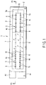
FIGS. 1 and2 illustrate anillumination apparatus 1. Theillumination apparatus 1 forms an LED package formed as a unit serving as one module. Theillumination apparatus 1 comprises abaseboard 2, areflective layer 3, acircuit pattern 4, a plurality of semiconductor light-emittingdevices 5, anadhesive layer 6, areflector 7, a sealingmember 8, and alight diffusion member 9. - The
baseboard 2 is a flat board formed of, for example, a synthetic resin, and is rectangular to obtain a light-emitting area necessary for theillumination apparatus 1. As illustrated inFIG. 2 , thebaseboard 2 has afront surface 2a, and aback surface 2b located on the reverse side of thefront surface 2a. Epoxy resin including glass powder is preferably used as material of thebaseboard 2. - The material of the
baseboard 2 is not limited to synthetic resin, but metal can also be used as the material of thebaseboard 2. When thebaseboard 2 is formed of metal, heat dissipation from theback surface 2b of thebaseboard 2 is improved, and temperature distribution of thebaseboard 2 is equalized. This structure is preferable to inhibit variation of color of light emitted from the semiconductor light-emittingdevices 5 which emit light of the same wavelength region. - To inhibit variation of color of emitted light, it is desirable to form the
baseboard 2 of a metal material having excellent heat conductivity. Examples of metal material having excellent heat conductivity are aluminum having a heat conductivity of 10 w/m·K or more, and an alloy thereof. - The
reflective layer 3 is layered on thefront surface 2a of thebaseboard 2, and has a size enough to arrange semiconductor light-emittingdevices 5 of a predetermined number thereon with intervals. Thereflective layer 3 is formed of a white insulating material. Prepreg in the form of a sheet is used as the insulating material. Prepreg is a material obtained by impregnating a sheet base material with thermosetting resin containing white powder such as aluminum oxide or the like, and has adhesion by itself. Therefore, thereflective layer 3 is adhered to thefront surface 2a of thebaseboard 2, and covers thebaseboard 2. Thereflective layer 3 has a flat lightreflective surface 3a which is disposed on a side not facing thebaseboard 2. - As illustrated in
FIG. 4 , thecircuit pattern 4 is formed on the lightreflective surface 3a of thereflective layer 3. Thecircuit pattern 4 has afist conductor line 4a and asecond conductor line 4b. The first andsecond conductor lines baseboard 2, and are arranged parallel to each other and separated by an interval. - The
first conductor line 4a has a plurality ofpads 4c serving as conductor parts, and a firstterminal part 4d. In the same manner, thesecond conductor line 4b has a plurality ofpads 4c serving as conductor parts, and a secondterminal part 4e. Thepads 4c are arranged longitudinally at intervals relative to thebaseboard 2. The firstterminal part 4d is formed as one unitary piece with thepad 4c located at one end of thefirst conductor line 4a. The secondterminal part 4e is formed as one unitary piece with thepad 4c located at one end of thesecond conductor line 4b. - The first and second
terminal parts baseboard 2. Further, the first and secondterminal parts reflective layer 3. A power supply cable is connected to each of the first and the secondterminal parts - The
circuit pattern 4 according to the first embodiment is formed by the following process. - First, a prepreg impregnated with uncured thermosetting resin is bonded onto the
front surface 2a of thebaseboard 2, and thefront surface 2a of thebaseboard 2 is covered with thereflective layer 3. Next, a copper foil having the same size as that of thereflective layer 3 is adhered onto thereflective layer 3, and thereby a laminated member is formed. Thereafter, the laminated member is heated and pressurized simultaneously, and thereby the thermosetting resin is cured. Thereby, thebaseboard 2 and the copper foil are bonded to thereflective layer 3 as one unitary piece. Then, a resist layer is superposed on the copper foil, and the copper foil is subjected to etching. Thereafter, the resist layer is removed, and thereby acircuit pattern 4 is formed on thereflective layer 3. The thickness A (refer toFIG. 3 ) of the copper foil forming thecircuit pattern 4 is, for example, 35 µm. - Double-wire blue LED chips using, for example, nitride semiconductor are used as the semiconductor light-emitting
devices 5. As illustrated inFIGS. 2 and3 , each of the semiconductor light-emittingdevices 5 has asubstrate 11 having a light-transmitting property, and a semiconductor light-emittinglayer 12. - For example, a sapphire substrate is used as the
substrate 11. Thesubstrate 11 has afirst surface 11a, and asecond surface 11b located on the reverse side of thefirst surface 11a. In the first embodiment, thefirst surface 11a and thesecond surface 11b are parallel to each other. The thickness B of thesubstrate 11 is, for example, 90 µm, which is larger than the thickness of thepads 4c of thecircuit pattern 4. - The semiconductor light-emitting
layer 12 is formed by successively stacking a buffer layer, an n-type semiconductor layer, a light-emitting layer, a p-type clad layer, and a p-type semiconductor layer on thefirst surface 11a of thesubstrate 11. The light-emitting layer has a quantum well structure obtained by alternately stacking barrier layers and a well layer. The n-type semiconductor layer has an n-side electrode 13. The p-type semiconductor layer has a p-side electrode 14. The semiconductor light-emittinglayer 12 of this type does not have a reflective film, and radiates light to both sides relative to the thickness. - As illustrated in
FIG. 1 , each of the semiconductor light-emittingdevices 5 is arranged betweenpads 4c which are adjacent to each other longitudinally relative to thebaseboard 2, and is bonded onto the same lightreflective surface 3a of thereflective layer 3 by theadhesive layer 6. Specifically, thesecond surface 11b of thesubstrate 11 of each semiconductorlight emitting device 5 is bonded onto the lightreflective surface 3a by theadhesive layer 6. As a result, thepads 4c of thecircuit pattern 4 and the semiconductor light-emittingdevices 5 are alternately arranged on the lightreflective surface 3a. - As illustrated in
FIGS. 2 and3 , each of the semiconductor light-emittingdevices 5 has a pair ofside surfaces side surface 5a of each semiconductor light-emittingdevice 5 is opposed to oneadjacent pad 4c. Theother side surface 5b of each semiconductor light-emittingdevice 5 is opposed to anotheradjacent pad 4c. - The thickness C of the
adhesive layer 6 interposed between the semiconductor light-emittingdevices 5 and the lightreflective surface 3a is, for example, 100 to 500 µm. A silicone-resin-based adhesive is preferably used as theadhesive layer 6. The silicone-resin-based adhesive has a light-transmitting property which achieves a light transmittance of 70% or more when the thickness is 100 µm or more, for example. - As illustrated in
FIGS. 2 and3 , theelectrodes device 5 are electrically connected to theadjacent pads 4c of thecircuit pattern 4 by wire bonding. Specifically, the n-side electrode 13 is electrically connected to apad 4c adjacent to theside surface 5a of the semiconductor light-emittingdevice 5 by abonding wire 15. The p-side electrode 14 is electrically connected to anotherpad 4c adjacent to theside surface 5b of the semiconductor light-emittingdevice 5 by thebonding wire 15. - Further, a
pad 4c which is located on a side reverse to the firstterminal part 4d in thefirst conductor line 4a is electrically connected with apad 4c which is located on a side reverse to the secondterminal part 4e in thesecond conductor line 4b by another bonding wire 16 (refer toFIG. 1 ). Therefore, according to the first embodiment, the semiconductor light-emittingdevices 5 are connected in series through thecircuit pattern 4. - As illustrated in
FIG. 1 , thereflector 7 is a rectangular frame, and surrounds all the semiconductor light-emittingdevices 5 on thereflective layer 3 by itself. In other words, thereflector 7 is not provided for each of the semiconductor light-emittingdevices 5, but serves as a constituent element common to all the semiconductor light-emittingdevices 5. - The
reflector 7 is bonded to the lightreflective surface 3a of thereflective layer 3. In the first embodiment, all the semiconductor light-emittingdevices 5 and all thepads 4 of thecircuit pattern 4 are located in a region surrounded by thereflector 7. The first and secondterminal parts circuit pattern 4 are located outside thereflector 7. - The
reflector 7 is formed of synthetic resin or the like, and an internal surface of thereflector 7 serves as a lightreflective surface 7a. The lightreflective surface 7a is formed by evaporating, or forming by plating, a metal material having high reflectance such as Al and Ni onto the internal surface of thereflector 7. The lightreflective surface 7a can also be formed by applying white paint having high visible light reflectance onto the internal surface of thereflector 7. - Further, the light
reflective surface 7a itself can be provided with a white color with high visible light reflectance, by mixing white powder into resin material forming thereflector 7. A white filler such as aluminum oxide, titanium oxide, magnesium oxide, and barium sulfate can be used as the white powder. As illustrated by chain double-dashed lines inFIG. 2 , the lightreflective surface 7a of thereflector 7 is preferably inclined toward the outside of thereflector 7 as it goes away from the lightreflective surface 3a of thereflective layer 3. - As illustrated in
FIG. 2 , the sealingmember 8 is injected into the region surrounded by thereflector 7. The sealingmember 8 is solidified in the state of covering the semiconductor light-emittingdevices 5, thepads 4c and thebonding wires member 8 is formed of a material having a light-transmitting property, such as a transparent silicone resin and a transparent glass. - Fluorescent particles are mixed into the material forming the sealing
member 8, if necessary. In the first embodiment, blue LED chips are used as the semiconductor light-emittingdevices 5. Therefore, used are fluorescent particles which perform wavelength conversion to convert blue primary light emitted from the blue LED chips into yellow secondary light having a different wavelength. As a preferably example, the fluorescent particles are mixed into the sealingmember 8 in the state of being almost uniformly dispersed in the sealingmember 8. - In the case of using the sealing
member 8 containing fluorescent particles, the fluorescent particles, which blue light emitted from the semiconductor light-emittinglayer 12 strikes, absorbs the blue light and emits yellow light. The yellow light passes through the sealingmember 8. On the other hand, part of the blue light radiated from the semiconductor light-emittinglayer 12 passes through the sealingmember 8, without striking the fluorescent particles. Therefore, light beams of two colors having a relationship of complementary colors are mixed, and thereby white light is obtained. - As illustrated in
FIG. 2 , thelight diffusion member 9 is flat and is disposed in front of thereflector 7. Thelight diffusion member 9 may be directly supported by thereflector 7, or may be supported by an illumination appliance (not shown) containing theillumination apparatus 1. - As the
light diffusion member 9, it is desirable to use a material having a light diffusion property, in which difference between transmittance for blue light having a wavelength of 400 to 480 nm and transmittance for yellow light having a wavelength of 540 to 650 nm is 10% or less, and visible light transmittance equal to or larger than 90% and less than 100%. By using thelight diffusion member 9 satisfying the above conditions, blue primary light and yellow secondary light are mixed by thelight diffusion member 9, and thereby white light is obtained with suppressed unevenness in color. - As illustrated in
FIG. 2 , the distance L between thelight diffusion member 9 and the lightreflective surface 3a, on which the semiconductor light-emittingdevices 5 are arranged, preferably falls within a range from 5 to 15 mm. - The inventor(s) of the present invention prepared an
illumination apparatus 1 using alight diffusion member 9 having transmittance of 90%, and anillumination apparatus 1 using alight diffusion member 9 having transmittance of 80%, and performed the following lighting test. In the lighting test, the total luminous flux was measured in each of the twoillumination apparatuses 1 under the conditions in which the distance L ranges from 5 to 15 mm, and the visual impression of thelight diffusion members 9 was evaluated. - The visual impression indicates whether the semiconductor light-emitting
devices 5 appear to individually emit light in a dotted manner. In the first embodiment, the visual impression is evaluated with criteria of "good" and "not good". - The "good" visual impression means that the semiconductor light-emitting
devices 5 do not appear to be individual dot light sources, and difference in brightness between parts of thelight diffusion member 9 corresponding to the semiconductor light-emittingdevices 5 and surrounding parts is small. Conversely, the "not good" visual impression means that the semiconductor light-emittingdevices 5 are clearly recognized as individual light sources, and difference in brightness between parts of thelight diffusion member 9 corresponding to the semiconductor light-emittingdevices 5 and surrounding parts is large. - The
illumination apparatus 1 using thelight diffusion member 9 having transmittance of 90% had the total luminous flux of 100 lm, and the visual impression thereof was evaluated as "good". Theillumination apparatus 1 using thelight diffusion member 9 having transmittance of 80% had the total luminous flux of 90 lm, and the visual impression thereof was evaluated as "good". This result shows that the transmittance of thelight diffusion member 9 is preferably set to 90% or more. - On the other hand, the inventor(s) of the present invention researched relationship between the total luminous flux and the visual impression when the distance L between the light
reflective surface 3a of thereflective layer 3 and thelight diffusion member 9 is varied, in theillumination apparatus 1 using thelight diffusion member 9 having transmittance of 90%. - As a result, when the distance L was less than 5 mm, the total luminous flux of the
illumination apparatus 1 was 105 lm, and the visual impression was "not good". When the distance L exceeded 15 mm, the total luminous flux was 95 lm, and the visual impression was "good". - Therefore, when the distance L is less than 5 mm, the semiconductor light-emitting
devices 5 become easily recognized as individual dot light sources. Conversely, when the distance L exceeds 15 mm, the brightness becomes insufficient. Therefore, it proved that setting the distance L to a range from 5 to 15 mm secures brightness necessary for illumination purposes, and prevents the semiconductor light-emittingdevices 5 from being viewed as individual dot light sources. - As a result, it is preferable from a practical standpoint to use
light diffusion member 9 having visible light transmittance of 90% or more in theillumination apparatus 1, and set the distance L between the lightreflective surface 3a of thereflective layer 3 and thelight diffusion member 9 to a range from 5 to 15 mm. - On the other hand, in the
illumination apparatus 1 of the first embodiment, the reflectance of the lightreflective surface 3a of thereflective layer 3 is preferably 85% or more in a region of a wavelength of 420 to 740 nm. When the reflectance is less than 85%, efficiency of reflecting light emitted from the semiconductor light-emittinglayers 12 toward thebaseboard 2 through thesubstrates 11 by the lightreflective surface 3a is low, and light of the semiconductor light-emittingdevices 5 is not efficiently obtained. -
FIG. 5 is a graph illustrating relationship between total light reflectance (%) of the white resin material used for thereflective layer 3 and wavelength (nm). InFIG. 5 , a solid line indicates total light reflectance of the white resin material, and a dotted line illustrates total light reflectance of silver as a comparative example. Silver has total light reflectance of 85% or more in the whole region of a wavelength of 400 to 740 nm. In comparison with this, the white resin material has total light reflectance of 35% at a wavelength of 400 nm, and has total light reflectance of 85% in a region of wavelength of 480 to 740 nm. However, the average of total light reflectance is 85% or more in the whole region of a wavelength of 420 to 740 nm, and thus light emitted from the semiconductor light-emittingdevices 5 can be efficiently and sufficiently delivered. - Further, to secure the heat radiation property of the
reflective layer 3 while securing the reflectance thereof, the thickness T of thereflective layer 3 is preferably set to a range from 30 to 90 µm. Table 1 illustrates reflectance at a wavelength of 460 nm, reflectance at a wavelength of 550 nm, and thermal resistance (°C/W) for each of the cases where the thickness T of thereflective layer 3 is set to 30, 90, and 120 µm. As is clear from Table 1, thereflective layer 3 shows a characteristic that the reflectance thereof decreases as the thickness T decreases, and the thermal resistance thereof increases as the thickness T increases.Table 1 Thickness Reflectance [460 nm] Reflectance [550 nm] Thermal resistance Rjs [°C/W] 30 80.56 85.79 550 90 83.44 86.69 600 120 84.88 87.14 700 - The life of semiconductor light-emitting
devices 5 is 40000 hours when used at a junction temperature of 100°C. Therefore, to lengthen the life of the semiconductor light-emittingdevices 5, the semiconductor light-emittingdevices 5 are preferably used at a junction temperature of 100°C or less. - Table 2 illustrates a relationship between the thickness T of the
reflective layer 3 and increase in temperature of thereflective layer 3, when the semiconductor light-emittingdevices 5 are lit up by applying electric power of 0.06W, in the case where a wattage per chip of the semiconductor light-emittingdevices 5 is 0.06W. As is clear from Table 1 and Table 2, since thermal resistance of thereflective layer 3 decreases as the thickness T of thereflective layer 3 decreases, heat conducted from the semiconductor light-emittingdevices 5 to thereflective layer 3 is efficiently diffused, and increase in temperature of thereflective layer 3 is prevented. In comparison with this, since thermal resistance of thereflective layer 3 increases as the thickness T of thereflective layer 3 increases, and thus increase in temperature of thereflective layer 3 is promoted.Table 2 Thickness Increase in temperature [°C] 30 33 90 36 120 42 - For example, in an enclosed illumination appliance using semiconductor light-emitting devices obtaining luminous flux of 5000 lm as light source, the atmospheric temperature in the appliance reaches 60 to 70°C. A value obtained by adding the atmospheric temperature to the value of increase in temperature shown in Table 2 is the junction temperature of the appliance. Therefore, when the thickness T of the
reflective layer 3 is 120 µm, the junction temperature exceeds 100°C. Therefore, to suppress the junction temperature not to exceed 100°C, it is necessary to set the thickness T of thereflective layer 3 to 90 µm or less. - On the other hand, when the thickness T of the
reflective layer 3 is reduced, light undesirably passes through thereflective layer 3, and thus light reflectance of thereflective layer 3 decreases. Table 3 illustrates a relationship between the thickness of thereflective layer 3 and total luminous flux (lm) per chip of the semiconductor light-emittingdevices 5. It is required that the percentage of decrease in the total luminous flux is suppressed to about 10%, supposing that a value of the total luminous flux when the thickness T of thereflective layer 3 is 120 µm is set as the maximum value. Therefore, the necessary thickness T of thereflective layer 3 is 30 µm or more.Table 3 Thickness Total luminous flux per chip [lm] Percentage [%] 30 5.74 93.3 90 6.01 97.7 120 6.15 100.0 - In consideration of the above, the thickness T of the
reflective layer 3 is preferably set to a value which falls within a range from 30 to 90 µm. Thereby, the heat radiation property of thereflective layer 3 is enhanced, while the reflectance of thereflective layer 3 is secured. - According to the first embodiment, the
substrates 11 of the semiconductor light-emittingdevices 5 are bonded onto the whitereflective layer 3, on which thepads 4c are formed, by the translucentadhesive layer 6. The semiconductor light-emittingdevices 5 are electrically connected to thepads 4, and held in a line on the lightreflective surface 3a of thereflective layer 3, with theadhesive layer 6 interposed therebetween. By the above structure, anillumination apparatus 1 which can perform surface emission is obtained. - According to the
illumination apparatus 1, part of light emitted from the semiconductor light-emittinglayer 12 of each semiconductor light-emittingdevice 5 passes through thesubstrate 11 and travels toward thereflective layer 3, which is reverse to the normal light guiding direction indicated by arrows inFIG. 2 . The light traveling toward thereflective layer 3 is made incident on a region of thereflective layer 3 corresponding to the projection area of thesubstrate 11 through theadhesive layer 6, and is reflected by the lightreflective surface 3a of thereflective layer 3 in the normal light guiding direction. - Further, among light traveling from the semiconductor light-emitting
layers 12 toward thereflective layer 3, light which has slantingly passed through thesubstrates 11 toward the surroundings of thesubstrates 11 is reflected by the lightreflective surface 3a located around thesubstrates 11 in the normal light guiding direction. - Simultaneously, when light emitted from the semiconductor light-emitting
layers 12 in the normal light guiding direction strikes the fluorescent particles inside the sealingmember 8, part of secondary light having yellow color travels toward thereflective layer 3. The yellow light traveling toward thereflective layer 3 is also reflected by the lightreflective surface 3a in the normal light guiding direction. - Therefore, light traveling from the semiconductor light-emitting
layers 12 toward thereflective layer 3 is reflected not only by parts of the lightreflective surface 3a corresponding to the respective semiconductor light-emittingdevices 5, but also by parts of the lightreflective surface 3a located outside the semiconductor light-emittingdevices 5 in the normal light guiding direction. Specifically, all the regions of the lightreflective surface 3a except regions covered with thepads 4c are used to reflect light traveling from the semiconductor light-emittinglayers 12 toward thereflective layer 3 in the normal light guiding direction. Therefore, light is efficiently delivered from theillumination apparatus 1. - Further, light emitted from the semiconductor light-emitting
layers 12 is radiated toward the surroundings of thesubstrates 11. Therefore, part of light made incident on thesubstrates 11 from the semiconductor light-emittinglayers 12 and part of light made incident on thesubstrates 11 again through theadhesive layer 6 after reflected by the lightreflective surface 3a of thereflective layer 3 are radiated to the outside of thesubstrates 11 through the first and second side surfaces 5a and 5b of the semiconductor light-emittingdevices 5. Thepads 4c which are electrically connected to the semiconductor light-emittingdevices 5 are located adjacent to the first and second side surfaces 5a and 5b of the semiconductor light-emittingdevices 5. Therefore, light radiated from the first and second side surfaces 5a and 5b may interfere with thepads 4c, and may be absorbed into thepads 4c. - However, according to the first embodiment, the thickness A of the
pads 4c is smaller than the thickness B of thesubstrates 11. Therefore, light radiated from the first and second side surfaces 5a and 5b of the semiconductor light-emittingdevices 5 toward thepads 4c does not easily interfere with thepads 4c, and loss of light is reduced. This structure has an advantage in efficient delivery of light. - Further, the
pads 4c of thecircuit pattern 4 and the semiconductor light-emittingdevices 5 are arranged longitudinally relative to thebaseboard 2. This structure reduces the total area of thepads 4c covering the light-reflective surface 3a of thereflective layer 3. Consequently, a substantial area of the lightreflective surface 3a which contributes to reflection is sufficiently secured, which is also advantageous in efficient delivery of light. - In addition, the
single reflector 7 surrounds all the semiconductor light-emittingdevices 5. This structure remarkably reduces the possibility that light emitted from the individual semiconductor light-emittingdevices 5 interferes with thereflector 7, and thus increases the amount of light traveling toward thelight diffusion member 9. In other words, light made incident on the lightreflective surface 7a of thereflector 7 is reduced, light is not easily absorbed into the lightreflective surface 7a, and loss of light due to absorption of light is reduced. Therefore, light emitted from the semiconductor light-emittingdevices 5 is efficiently delivered. - For example, if a reflector having a radially-spreading reflective surface is provided for each of, or each group of, semiconductor light-emitting devices, light radiated from respective semiconductor light-emitting devices are made incident on the light reflective surfaces of the respective reflectors. Therefore, amount of light made incident on the reflectors increases, and the probability that light is absorbed into the light reflective surface is increased. Thus, loss of light is increased, and light emitted from the semiconductor light-emitting devices cannot be efficiently delivered.
- The efficiency of delivering light was evaluated by the following comparison. The illumination apparatus used in this comparison has a baseboard made of aluminum, and reflectance of the reflective layer thereof is 90% for light of a wavelength of 400 to 740 nm. Further, a die bond material having a 100 µm thickness and 95% transmittance was used as the adhesive layer, 28 semiconductor light-emitting devices were arranged on the reflective layer, and a single reflector surrounded all the semiconductor light-emitting devices by oneself. The luminous flux when the illumination apparatus is lit by energizing it with 20 mA was 120 lm.
- In comparison with this, an illumination apparatus serving as a comparative example had a structure in which 28 reflectors were provided, and the reflectors included respective semiconductor light-emitting devices. The luminous flux of the illumination apparatus when the illumination apparatus was lit by energizing it with 20 mA was 110 lm.
- In the
illumination apparatus 1 of the first embodiment, a plurality ofbonding wires 15 runs between the lightreflective surface 3a of thereflective layer 3 and thelight diffusion member 9. Therefore, part of light which is reflected by the lightreflective surface 3a and travels toward thelight diffusion member 9 is obstructed by thebonding wires 15. - According to the first embodiment, the
bonding wires 15 connect adjacent semiconductor light-emittingdevices 5 in series. Therefore, the number of thebonding wires 15 is reduced, in comparison with the case where a plurality of semiconductor light-emittingdevices 5 are connected in parallel by bondingwires 15. Thereby, this structure is advantageous in efficiently delivering light emitted from the semiconductor light-emittingdevices 5. - When a plurality of semiconductor light-emitting devices are connected in parallel, it is necessary to form a plurality of pattern parts in a straight line on the
reflective layer 3 along the arranging direction of the semiconductor light-emittingdevices 5, and electrically connect the pattern parts and the respective semiconductor light-emittingdevices 5 by respective bonding wires. This structure reduces the area of a part of the lightreflective surface 3a which actually contributes to reflection, and is not preferable in consideration of delivery of light. - In the
illumination apparatus 1 according to the first embodiment, a plurality of semiconductor light-emittingdevices 5 are bonded onto thereflective layer 3 on which thecircuit pattern 4 is formed. Therefore, it is unnecessary to individually form a plurality of reflective layers corresponding to the respective semiconductor light-emittingdevices 5 on thebaseboard 2. Therefore, thereflective layer 3 can be easily formed without special process, and the manufacturing cost of theillumination apparatus 1 is reduced. - More specifically, in the conventional structure in which light of the semiconductor light-emitting devices is reflected by using white insulating adhesive including a white filler, it is required to precisely apply a small amount of insulating adhesive for each of minute semiconductor light-emitting devices. This deteriorates the workability, and requires much labor and time in work. Further, to control the thickness and the application area of the insulating adhesive to a specified value incurs much difficulty also in respect of manufacturing technology.
- In comparison with this, in the
illumination apparatus 1 of the first embodiment, thereflective layer 3 only continuously covers thesurface 2a of thebaseboard 2. Therefore, no technically difficult work is required for forming thereflective layer 3. Therefore, thereflective layer 3 is easily formed on thebaseboard 2, and the manufacturing cost of theillumination apparatus 1 is reduced. - In addition, in prior art, since work of applying insulating adhesive incurs much difficulty, the thickness of insulating adhesive applied to individual semiconductor light-emitting devices becomes nonuniform, and variations in the thermal resistance of the insulating adhesive is inevitable. This causes a slight difference in heat radiation properties between the semiconductor light-emitting devices, and the color of light emitted from the semiconductor light-emitting devices may vary.
- In comparison with this, according to the
illumination apparatus 1 of the first embodiment, thereflective layer 3 is superposed with a predetermined thickness on thesurface 2a to cover the wholefront surface 2a of thebaseboard 2. Therefore, thereflective layer 3 does not have an adverse influence on the heat radiation property of the semiconductor light-emittingdevices 5. This structure prevents a slight difference in color of emitted light of the semiconductor light-emittingdevices 5. - The present invention is not limited to the above first embodiment, but can be carried out with various modifications within a range not departing from the gist of the invention.
-
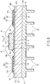
FIGS. 6 to 8 illustrate anillumination apparatus 21 according to the second embodiment of the present invention. Theillumination apparatus 21 is different from the illumination apparatus of the first embodiment mainly in the structure for increasing the heat radiation property of the semiconductor light-emittingdevices 5. The other parts of theillumination apparatus 21 are basically the same as those in the first embodiment. Therefore, in the second embodiment, constituent elements which are the same as those in the first embodiment are denoted by the same respective reference numerals, and explanation thereof is omitted. - As illustrated in
FIGS. 6 to 8 , abaseboard 22 is a flat metal board, and is rectangular to secure a light emission area necessary for theillumination apparatus 21. Thebaseboard 22 has afront surface 22a, and aback surface 22b located on the reverse side of thefront surface 22a. Thebaseboard 22 is preferably formed of copper which has excellent thermal conductivity. - A
reflective layer 23 is superposed on thefront surface 22a of thebaseboard 22. Thereflective layer 23 is formed by plating thebaseboard 22 with silver, and has conductivity. Thereflective layer 23 covers the wholefront surface 22a of thebaseboard 22, and has a sufficient size on which a predetermined number of semiconductor light-emittingdevices 5 are arranged at intervals. Thereflective layer 23 has a flat lightreflective surface 23a which is located on a side not facing thebaseboard 22. - The diffusion reflectance of the light
reflective surface 23a is preferably 70% or more in a region of a wavelength of 420 to 740 nm. The diffusion reflectance is evaluated with a value supposing that the diffusion reflectance of white barium sulfate is 100%. When the diffusion reflectance of the lightreflective surface 23a is 70% or more, the average of total light reflectance of the lightreflective surface 23a in the region of a wavelength of 420 to 740 nm exceeds 85%. Therefore, light is efficiently delivered. - A
circuit pattern 24 is formed on the lightreflective surface 23a of thereflective layer 23. Thecircuit pattern 24 has a plurality of conductor lines 25. The conductor lines 25 extend longitudinally relative to thebaseboard 22, and are arranged parallel to and separated from each other. - Each
conductor line 25 has a plurality ofpads 25a serving as conductor parts, a firstterminal part 25b, and a secondterminal part 25c. Thepads 25a are arranged at intervals longitudinally relative to thebaseboard 22. The firstterminal part 25b is formed as one unitary piece with apad 25a located at one end of eachconductor line 25. The secondterminal part 25c is formed as one unitary piece with apad 25a located at the other end of eachconductor line 25. Therefore, the firstterminal part 25b and the secondterminal part 25c are separated from each other longitudinally relative to eachconductor line 25. - As illustrated in
FIG. 8 , eachpad 25a has aninsulator 27 and aconductive layer 28. For example, ceramic is used as theinsulator 27. Theinsulator 27 has afirst surface 27a and asecond surface 27b located on the reverse side of thefirst surface 27a. Thefirst surface 27a and thesecond surface 27b are parallel to each other. Theconductor layer 28 is formed by plating thefirst surface 27a with gold or the like. - Each
pad 25a is bonded onto the lightreflective surface 23a of thereflective layer 23 by an insulatingadhesive 29. The insulatingadhesive 29 is filled between thesecond surface 27b of theinsulator 27 and the lightreflective surface 23a, and holds theinsulator 27 on the lightreflective surface 23a. Therefore, a space between theconductive layer 28 of eachpad 25a and thereflective layer 23 formed of silver plating is maintained at an electrically insulated state. - The first and second
terminal parts circuit pattern 24 have the same structure as that of theabove pads 25a, and explanation thereof is omitted. - Semiconductor light-emitting
devices 5 which are the same as those in the first embodiment are arranged on the lightreflective surface 23a of thereflective layer 23. Each semiconductor light-emittingdevice 5 is located between twopads 25a which are longitudinally adjacent relative to thebaseboard 22, and bonded onto the lightreflective surface 23a of thereflective layer 23 by theadhesive layer 6. - As illustrated in
FIG. 8 , an n-side electrode 13 of each semiconductor light-emittingdevice 5 is electrically connected to theconductive layer 28 of apad 25a adjacent to aside surface 5a of the semiconductor light-emittingdevice 5 by abonding wire 15. A p-side electrode 14 of each semiconductor light-emittingdevice 5 is electrically connected to theconductive layer 28 of apad 25a adjacent to aside surface 5b of the semiconductor light-emittingdevice 5 by thebonding wire 15. Therefore, the semiconductor light-emittingdevices 5 are connected in series in each of the conductor lines 25 of thecircuit pattern 24. - As illustrated in
FIGS. 7 and8 , aheat sink 31 is attached to theback surface 22b of thebaseboard 22. Theheat sink 31 has a heat-receivingboard 32 and a plurality of heat-radiatingfins 33. - The heat-receiving
board 32 has a size enough to cover thewhole back surface 22b of thebaseboard 22. The heat-receivingboard 32 is fixed on theback surface 22b of thebaseboard 22 by means of bonding or the like, and thermally connected to thebaseboard 22. The heat-radiatingfins 33 are formed as one unitary piece with the heat-receivingboard 32. The heat-radiatingfins 33 project from the heat-receivingboard 32 toward the side reverse to thebaseboard 22. - In the second embodiment, when the semiconductor light-emitting
devices 5 emit light, the semiconductor light-emittingdevices 5 generate heat. The semiconductor light-emittingdevices 5 are bonded onto thereflective layer 23 formed of silver plating, and are thermally connected to thereflective layer 23. Therefore, heat generated by the semiconductor light-emittingdevices 5 is directly conducted to thereflective layer 23 through theadhesive layer 6. - The
reflective layer 23 formed of silver plating has high thermal conductivity in comparison with the resinreflective layer 3 of the first embodiment. Therefore, the thermal resistance of a package formed by incorporating the semiconductor light-emittingdevices 5 with thebaseboard 22 is reduced. - The thermal resistance of the package is evaluated by the following expression, when the temperature of the semiconductor light-emitting
devices 5 when they are lit is Tj, and the temperature of the package when the semiconductor light-emittingdevices 5 are lit is Tc:
- The inventor(s) of the present invention mounted 100 semiconductor light-emitting devices having a power rating of 20 mA on a reflective layer, and tested the thermal resistance of the package when the semiconductor light-emitting devices were lit up by supplying electric power of 6.0W.
- As a result, the package using a
reflective layer 23 formed of silver plating had a thermal resistance of 0.6 °C/W, and the package using areflective layer 3 formed of resin had a thermal resistance of 7.0 °C/W. - In view of the above, the
reflective layer 23 formed of silver plating has better thermal conductivity than thereflective layer 3 formed of resin, and can efficiently relieve heat of the semiconductor light-emittingdevices 5 to thebaseboard 22. - Further, according to the second embodiment, heat of each semiconductor light-emitting
device 5 is conducted to theadjacent pads 25a through thebonding wires 15. Since thepads 25a are bonded to thereflective layer 23 formed of silver plating, thepads 25a are maintained at a state of being thermally connected to thereflective layer 23. Therefore, the heat of the semiconductor light-emittingdevices 5 conducted to thepads 25a through thebonding wire 15 is conducted to thereflective layer 23 through the insulatingadhesive 29. Therefore, part of heat generated by the semiconductor light-emittingdevices 5 is relieved from thepads 25a to thereflective layer 23. - As a result, heat of the semiconductor light-emitting
devices 5 is smoothly diffused into thebaseboard 22 through thereflective layer 23. Therefore, the semiconductor light-emittingdevices 5 are prevented from overheating, and the atmospheric temperature of the semiconductor light-emittingdevices 5 is maintained at a proper temperature. - In addition, according to the second embodiment, the
heat sink 31 is provided on theback surface 22b of thebaseboard 22. Theheat sink 31 receives heat from thebaseboard 22, and radiates the heat from the heat-radiatingfins 33 into the atmosphere. - Therefore, heat relieved from the semiconductor light-emitting
devices 5 to thebaseboard 22 through thereflective layer 23 is smoothly radiated to the outside of theillumination apparatus 1 through theheat sink 31. This improves the heat-radiating property of thebaseboard 22, and thus is preferable in suppressing increase in temperature of the semiconductor light-emittingdevices 5. - The present application discloses:
- 1. An illumination apparatus comprising:
- a plurality of semiconductor light-emitting devices (5) each having a translucent substrate (11) and a semiconductor light-emitting layer (12) formed on the substrate (11);
- a white reflective layer (3, 23) having a size on which the semiconductor light-emitting devices (5) are arranged at intervals;
- a plurality of conductor parts (4c, 25a) to which the semiconductor light-emitting devices (5) are electrically connected, the conductor parts (4c, 25a) being provided on the reflective layer (3, 23); and
- a translucent adhesive layer (6) which bonds the substrate (11) of each of the semiconductor light-emitting devices (5) onto the reflective layer (3, 23), and thereby holds the semiconductor light-emitting devices (5) on the reflective layer (3, 23).
- 2. An illumination apparatus of
paragraph 1, wherein
the conductor parts (4c, 25a) are provided on the reflective layer (3, 23) to be adjacent to the semiconductor light-emitting devices (5), and a thickness of the substrates (11) of the semiconductor light-emitting devices (5) is larger than a thickness of the conductor parts (4c, 25a). - 3. An illumination apparatus of
paragraph
a light diffusion member (9) which diffuses light emitted from the semiconductor light-emitting devices (5), the light diffusion member (9) being opposed to the reflective layer (3). - 4. An illumination apparatus of
paragraph
the reflective layer (3) also serves as an insulating layer, and a thickness of the insulating layer falls within a range from 30 to 90 µm. - 5. An illumination apparatus of
paragraph 1, wherein
the reflective layer (23) is formed of silver plating. - 6. An illumination apparatus of
paragraph 5, wherein
the substrates (11) of the semiconductor light-emitting devices (5) and the conductor parts (25a) are thermally connected to the reflective layer (23), and the semiconductor light-emitting layers (12) of the semiconductor light-emitting devices (5) are electrically and thermally connected to the conductive parts (25a) by bonding wires (15).
Claims (15)
- An illumination apparatus comprising:- a plurality of semiconductor light-emitting devices (5) each having a translucent substrate (11) and a semiconductor light-emitting layer (12) formed on the substrate (11);- a reflective layer (23) having a size on which the semiconductor light-emitting devices (5) are arranged at intervals;- a reflector (7) formed of a synthetic resin or the like, wherein an internal surface of the reflector (7) serves as a light reflective surface (7a),- a plurality of conductor parts (4c, 25a) to which the semiconductor light-emitting devices (5) are electrically connected, the conductor parts (4c, 25a) being provided on the reflective layer (23) ; and- a translucent adhesive layer (6) which bonds the substrate (11) of each of the semiconductor light-emitting devices (5) onto the reflective layer (3, 23), and thereby holds the semiconductor light-emitting devices (5) on the reflective layer (23),characterized in that- the light reflective surface of the reflector (7) is provided with a white color with high visible light reflectance, by mixing white powder into a resin material forming the reflector (7).
- An illumination apparatus according to the preceding claim, wherein the reflective layer (23) is superposed on a front surface (22a) of a baseboard (22) and wherein the reflector layer (23) has a flat light reflective surface (23a) which is located on a side not facing the baseboard (22).
- An illumination apparatus according to one of the preceding claims, wherein the reflector (7) is bonded to the light reflective surface (23a) of the reflective layer (23) .
- An illumination apparatus according to one of the preceding claims, wherein the reflector (7) serves as a constituent element common to all the semiconductor light-emitting devices (5).
- An illumination apparatus according to one of the preceding claims, wherein the white powder comprises a white filler material, for instance aluminum oxide, titanium oxide, magnesium oxide and/or barium sulfate.
- An illumination apparatus according to one of the preceding claims, wherein the semiconductor light-emitting devices (5) are electrically connected to each other in a combination of an in series connection and an in parallel connection.
- An illumination apparatus according to one of the preceding claims, wherein a circuit pattern (24) having a plurality of conductor lines (25) is formed on the light reflective surface (23a) of the reflective layer (23), wherein the conductor lines (25) extend longitudinally relative to the baseboard (22) of the illumination apparatus and are arranged parallel to and separated from each other.
- An illumination apparatus according to claim 8, wherein the semiconductor light emitting devices (5) are connected in series in each of the conductor lines (25) of the circuit pattern (24).
- An illumination apparatus according to one of the preceding claims, wherein the conductor parts (4c) are provided on the reflective layer adjacent to the semiconductor light emitting devices (5).
- An illumination apparatus according to one of the preceding claims, wherein the thickness of the substrates (11) of the semiconductor light-emitting devices (5) is larger than a thickness of the conductor parts (4c).
- An illumination apparatus according to one of the preceding claims, further comprising a sealing member (8) formed of a material having a light-transmitting property and wherein fluorescent particles are mixed into the material forming the sealing member.
- An illumination apparatus according to one of the preceding claims, wherein the reflective layer (23) is formed of silver plating.
- An illumination apparatus according to one of the preceding claims, wherein the conductor parts are bonded onto the reflective layer (23) by an electrically insulating adhesive.
- An illumination apparatus according to one of the preceding claims, wherein the reflective layer (23) covers the whole front surface (22a) of the baseboard (22) and has a sufficient size on which a predetermined number of semiconductor light-emitting devices (5) are arranged at intervals.
- An illumination apparatus according to one of the preceding claims, wherein the translucent substrate (11) of the semiconductor light-emitting devices (5) is a crystalline sapphire substrate.
Applications Claiming Priority (2)
| Application Number | Priority Date | Filing Date | Title |
|---|---|---|---|
| JP2006232634 | 2006-08-29 | ||
| EP07253338.3A EP1895602B1 (en) | 2006-08-29 | 2007-08-23 | Illumination apparatus having a plurality of semiconductor light-emitting devices |
Related Parent Applications (2)
| Application Number | Title | Priority Date | Filing Date |
|---|---|---|---|
| EP07253338.3A Division-Into EP1895602B1 (en) | 2006-08-29 | 2007-08-23 | Illumination apparatus having a plurality of semiconductor light-emitting devices |
| EP07253338.3A Division EP1895602B1 (en) | 2006-08-29 | 2007-08-23 | Illumination apparatus having a plurality of semiconductor light-emitting devices |
Publications (1)
| Publication Number | Publication Date |
|---|---|
| EP3489572A1 true EP3489572A1 (en) | 2019-05-29 |
Family
ID=38738790
Family Applications (2)
| Application Number | Title | Priority Date | Filing Date |
|---|---|---|---|
| EP18212110.3A Withdrawn EP3489572A1 (en) | 2006-08-29 | 2007-08-23 | Illumination apparatus having a plurality of semiconductor light-emitting devices |
| EP07253338.3A Expired - Fee Related EP1895602B1 (en) | 2006-08-29 | 2007-08-23 | Illumination apparatus having a plurality of semiconductor light-emitting devices |
Family Applications After (1)
| Application Number | Title | Priority Date | Filing Date |
|---|---|---|---|
| EP07253338.3A Expired - Fee Related EP1895602B1 (en) | 2006-08-29 | 2007-08-23 | Illumination apparatus having a plurality of semiconductor light-emitting devices |
Country Status (4)
| Country | Link |
|---|---|
| US (2) | US7989840B2 (en) |
| EP (2) | EP3489572A1 (en) |
| JP (1) | JP5273486B2 (en) |
| CN (1) | CN100539134C (en) |
Families Citing this family (34)
| Publication number | Priority date | Publication date | Assignee | Title |
|---|---|---|---|---|
| EP1928026A1 (en) * | 2006-11-30 | 2008-06-04 | Toshiba Lighting & Technology Corporation | Illumination device with semiconductor light-emitting elements |
| JP5244680B2 (en) * | 2008-04-14 | 2013-07-24 | 株式会社半導体エネルギー研究所 | Method for manufacturing light emitting device |
| US8567988B2 (en) | 2008-09-29 | 2013-10-29 | Bridgelux, Inc. | Efficient LED array |
| CN102165011B (en) * | 2008-09-30 | 2013-09-04 | 日立化成工业株式会社 | Coating agent, substrate for mounting optical semiconductor element using same, and optical semiconductor device |
| SG166006A1 (en) * | 2009-04-07 | 2010-11-29 | Lim Boon Kiat | Matrix light illumination apparatus |
| US8408738B2 (en) * | 2009-04-21 | 2013-04-02 | Lg Electronics Inc. | Light emitting device |
| JP5499325B2 (en) | 2009-06-01 | 2014-05-21 | 東芝ライテック株式会社 | Light emitting module and lighting device |
| TWM374648U (en) * | 2009-10-15 | 2010-02-21 | Forward Electronics Co Ltd | AC LED packaging structure |
| JP2011091126A (en) * | 2009-10-21 | 2011-05-06 | Shin-Etsu Astech Co Ltd | Light emitting device (cob module) |
| CN102072811A (en) * | 2009-11-20 | 2011-05-25 | 广镓光电股份有限公司 | Optical detection device and detection method by applying same |
| JP4814394B2 (en) * | 2010-03-05 | 2011-11-16 | シャープ株式会社 | Method for manufacturing light emitting device |
| JP5485112B2 (en) * | 2010-11-02 | 2014-05-07 | 信越化学工業株式会社 | Manufacturing method of optical semiconductor device |
| US10267506B2 (en) | 2010-11-22 | 2019-04-23 | Cree, Inc. | Solid state lighting apparatuses with non-uniformly spaced emitters for improved heat distribution, system having the same, and methods having the same |
| CN103348496A (en) | 2011-02-07 | 2013-10-09 | 克利公司 | Components and methods for light emitting diode (LED) lighting |
| US20130099263A1 (en) * | 2011-10-20 | 2013-04-25 | Gregory Lee Heacock | Full spectrum led light source |
| US9786825B2 (en) * | 2012-02-07 | 2017-10-10 | Cree, Inc. | Ceramic-based light emitting diode (LED) devices, components, and methods |
| US9806246B2 (en) | 2012-02-07 | 2017-10-31 | Cree, Inc. | Ceramic-based light emitting diode (LED) devices, components, and methods |
| US9538590B2 (en) | 2012-03-30 | 2017-01-03 | Cree, Inc. | Solid state lighting apparatuses, systems, and related methods |
| WO2014048553A2 (en) * | 2012-09-26 | 2014-04-03 | Daniel Muessli | Led lighting devices and methods of manufacturing the same |
| WO2014093813A1 (en) * | 2012-12-14 | 2014-06-19 | Cree, Inc. | Ceramic-based light emitting diode (led) devices, components and methods |
| USD738542S1 (en) | 2013-04-19 | 2015-09-08 | Cree, Inc. | Light emitting unit |
| CN104061477B (en) * | 2014-07-08 | 2016-02-17 | 惠州奔达电子有限公司 | A kind of LED light source module of high efficiency and heat radiation |
| DE102014110054A1 (en) | 2014-07-17 | 2016-01-21 | Osram Oled Gmbh | Optoelectronic assembly and method for manufacturing an optoelectronic assembly |
| JP6256699B2 (en) * | 2014-11-11 | 2018-01-10 | 豊田合成株式会社 | Light emitting device |
| US9826581B2 (en) | 2014-12-05 | 2017-11-21 | Cree, Inc. | Voltage configurable solid state lighting apparatuses, systems, and related methods |
| JP6497615B2 (en) * | 2015-03-04 | 2019-04-10 | パナソニックIpマネジメント株式会社 | Mounting board and LED module using the same |
| JP6501564B2 (en) * | 2015-03-10 | 2019-04-17 | シチズン電子株式会社 | Light emitting device |
| CN106151905A (en) * | 2016-08-15 | 2016-11-23 | 浙江阳光美加照明有限公司 | A kind of LED light-emitting filament and the LEDbulb lamp using this LED light-emitting filament |
| USD823492S1 (en) | 2016-10-04 | 2018-07-17 | Cree, Inc. | Light emitting device |
| JP6868388B2 (en) * | 2016-12-26 | 2021-05-12 | 日亜化学工業株式会社 | Light emitting device and integrated light emitting device |
| KR102631105B1 (en) * | 2017-08-31 | 2024-01-30 | 니치아 카가쿠 고교 가부시키가이샤 | Light emitting device |
| JP7177331B2 (en) | 2018-06-29 | 2022-11-24 | 日亜化学工業株式会社 | light emitting device |
| JP7239804B2 (en) * | 2018-08-31 | 2023-03-15 | 日亜化学工業株式会社 | LENS, LIGHT-EMITTING DEVICE AND MANUFACTURING METHOD THEREOF |
| JP7288343B2 (en) * | 2019-05-16 | 2023-06-07 | スタンレー電気株式会社 | light emitting device |
Citations (6)
| Publication number | Priority date | Publication date | Assignee | Title |
|---|---|---|---|---|
| JPS5218190A (en) * | 1975-08-01 | 1977-02-10 | Toshiba Corp | Solid-state luminescent display |
| JP3329573B2 (en) | 1994-04-18 | 2002-09-30 | 日亜化学工業株式会社 | LED display |
| WO2004031844A1 (en) * | 2002-09-30 | 2004-04-15 | Siemens Aktiengesellschaft | Illumination device for backlighting an image reproduction device |
| EP1590994A2 (en) * | 2003-02-07 | 2005-11-02 | Matsushita Electric Industrial Co., Ltd. | Metal base wiring board for retaining light emitting elements, light emitting source, lighting apparatus, and display apparatus |
| JP2006041380A (en) * | 2004-07-29 | 2006-02-09 | Nippon Leiz Co Ltd | Light source device |
| JP2006173326A (en) * | 2004-12-15 | 2006-06-29 | Nippon Leiz Co Ltd | Optical source apparatus |
Family Cites Families (34)
| Publication number | Priority date | Publication date | Assignee | Title |
|---|---|---|---|---|
| US4729076A (en) * | 1984-11-15 | 1988-03-01 | Tsuzawa Masami | Signal light unit having heat dissipating function |
| JP2604490B2 (en) | 1990-07-03 | 1997-04-30 | 茨城日本電気株式会社 | Magnetic disk drive |
| JPH08264840A (en) | 1995-03-27 | 1996-10-11 | Sanyo Electric Co Ltd | Light emitting diode display device |
| JP3187280B2 (en) * | 1995-05-23 | 2001-07-11 | シャープ株式会社 | Surface lighting device |
| US5863109A (en) * | 1995-11-16 | 1999-01-26 | Hsieh; Chung-Tai | Phantom color light mirror |
| US6034712A (en) * | 1996-06-26 | 2000-03-07 | Brother Kogyo Kabushiki Kaisha | Exposure apparatus and image forming machine including it |
| US5954423A (en) * | 1997-05-02 | 1999-09-21 | Nsi Enterprises, Inc. | Light distribution diffuser for exit signs and the like illuminated by LED arrays |
| JP3785820B2 (en) * | 1998-08-03 | 2006-06-14 | 豊田合成株式会社 | Light emitting device |
| US6517218B2 (en) * | 2000-03-31 | 2003-02-11 | Relume Corporation | LED integrated heat sink |
| JP4432275B2 (en) | 2000-07-13 | 2010-03-17 | パナソニック電工株式会社 | Light source device |
| US6874910B2 (en) * | 2001-04-12 | 2005-04-05 | Matsushita Electric Works, Ltd. | Light source device using LED, and method of producing same |
| JP2005235779A (en) | 2001-08-09 | 2005-09-02 | Matsushita Electric Ind Co Ltd | Led lighting fixture and card type led lighting light source |
| TW567619B (en) * | 2001-08-09 | 2003-12-21 | Matsushita Electric Ind Co Ltd | LED lighting apparatus and card-type LED light source |
| JP4045781B2 (en) * | 2001-08-28 | 2008-02-13 | 松下電工株式会社 | Light emitting device |
| JPWO2003030274A1 (en) | 2001-09-27 | 2005-01-20 | 日亜化学工業株式会社 | Light emitting device and manufacturing method thereof |
| US7072096B2 (en) | 2001-12-14 | 2006-07-04 | Digital Optics International, Corporation | Uniform illumination system |
| US7121675B2 (en) * | 2002-01-10 | 2006-10-17 | Artak Ter-Hovhannisian | Low temperature LED lighting system |
| US6936855B1 (en) * | 2002-01-16 | 2005-08-30 | Shane Harrah | Bendable high flux LED array |
| JP2005056941A (en) * | 2003-08-07 | 2005-03-03 | Citizen Electronics Co Ltd | Light emitting diode |
| CN2665934Y (en) | 2003-09-25 | 2004-12-22 | 洪瑞华 | High-brightness LED with reflection mirror on electroplated substrate |
| KR100587328B1 (en) * | 2003-10-16 | 2006-06-08 | 엘지전자 주식회사 | Light Emitting Diode a front optical source |
| JP2005159262A (en) * | 2003-10-30 | 2005-06-16 | Kyocera Corp | Package for housing light emitting element, light emitting device, and lighting system |
| US7321161B2 (en) * | 2003-12-19 | 2008-01-22 | Philips Lumileds Lighting Company, Llc | LED package assembly with datum reference feature |
| JP4587675B2 (en) * | 2004-01-23 | 2010-11-24 | 京セラ株式会社 | Light emitting element storage package and light emitting device |
| US20050274971A1 (en) * | 2004-06-10 | 2005-12-15 | Pai-Hsiang Wang | Light emitting diode and method of making the same |
| JP2006093399A (en) | 2004-09-24 | 2006-04-06 | Kyocera Corp | Light-emitting device, its manufacturing method and luminaire |
| JP2006108240A (en) * | 2004-10-01 | 2006-04-20 | Fujikura Ltd | Illumination lamp and its manufacturing method |
| JP2006107850A (en) * | 2004-10-01 | 2006-04-20 | Rohm Co Ltd | Lighting device |
| JP5060707B2 (en) | 2004-11-10 | 2012-10-31 | 日立化成工業株式会社 | Thermosetting resin composition for light reflection |
| JP2006179572A (en) * | 2004-12-21 | 2006-07-06 | Sharp Corp | Light emitting diode, backlight device and method of manufacturing the light emitting diode |
| KR101093324B1 (en) | 2005-05-30 | 2011-12-14 | 엘지이노텍 주식회사 | Back light unit having light emitting diode |
| KR100592508B1 (en) * | 2005-07-15 | 2006-06-26 | 한국광기술원 | High power led package with beacon type substrate |
| JP2007116117A (en) | 2005-09-20 | 2007-05-10 | Toshiba Lighting & Technology Corp | Light emitting device |
| TWI296037B (en) * | 2006-04-28 | 2008-04-21 | Delta Electronics Inc | Light emitting apparatus |
-
2007
- 2007-08-23 US US11/844,037 patent/US7989840B2/en not_active Expired - Fee Related
- 2007-08-23 EP EP18212110.3A patent/EP3489572A1/en not_active Withdrawn
- 2007-08-23 EP EP07253338.3A patent/EP1895602B1/en not_active Expired - Fee Related
- 2007-08-28 CN CNB2007101455841A patent/CN100539134C/en not_active Expired - Fee Related
-
2010
- 2010-06-25 JP JP2010145090A patent/JP5273486B2/en active Active
-
2011
- 2011-07-15 US US13/184,320 patent/US8558272B2/en not_active Expired - Fee Related
Patent Citations (6)
| Publication number | Priority date | Publication date | Assignee | Title |
|---|---|---|---|---|
| JPS5218190A (en) * | 1975-08-01 | 1977-02-10 | Toshiba Corp | Solid-state luminescent display |
| JP3329573B2 (en) | 1994-04-18 | 2002-09-30 | 日亜化学工業株式会社 | LED display |
| WO2004031844A1 (en) * | 2002-09-30 | 2004-04-15 | Siemens Aktiengesellschaft | Illumination device for backlighting an image reproduction device |
| EP1590994A2 (en) * | 2003-02-07 | 2005-11-02 | Matsushita Electric Industrial Co., Ltd. | Metal base wiring board for retaining light emitting elements, light emitting source, lighting apparatus, and display apparatus |
| JP2006041380A (en) * | 2004-07-29 | 2006-02-09 | Nippon Leiz Co Ltd | Light source device |
| JP2006173326A (en) * | 2004-12-15 | 2006-06-29 | Nippon Leiz Co Ltd | Optical source apparatus |
Also Published As
| Publication number | Publication date |
|---|---|
| EP1895602B1 (en) | 2019-01-23 |
| CN100539134C (en) | 2009-09-09 |
| US8558272B2 (en) | 2013-10-15 |
| JP2010219562A (en) | 2010-09-30 |
| CN101136399A (en) | 2008-03-05 |
| JP5273486B2 (en) | 2013-08-28 |
| EP1895602A2 (en) | 2008-03-05 |
| US20080055901A1 (en) | 2008-03-06 |
| EP1895602A3 (en) | 2011-11-23 |
| US20110273880A1 (en) | 2011-11-10 |
| US7989840B2 (en) | 2011-08-02 |
Similar Documents
| Publication | Publication Date | Title |
|---|---|---|
| EP1895602B1 (en) | Illumination apparatus having a plurality of semiconductor light-emitting devices | |
| JP4678391B2 (en) | Lighting equipment | |
| JP5768435B2 (en) | Light emitting device | |
| US8690392B2 (en) | Light source unit and lighting system | |
| US7791091B2 (en) | Semiconductor light-emitting device, light-emitting module and lighting unit | |
| TWI581450B (en) | Semiconductor light emitting module and manufacturing method thereof | |
| JP4771179B2 (en) | Lighting device | |
| US8369375B2 (en) | Semiconductor light-emitting device | |
| JP5554680B2 (en) | Light-emitting element mounting substrate, light-emitting device, and manufacturing method thereof | |
| JP2010526425A (en) | Semiconductor light emitting device, and light source device and illumination system using the same | |
| JP2008244165A (en) | Lighting system | |
| JP4604819B2 (en) | Light emitting device | |
| JP5568476B2 (en) | Optoelectronic parts | |
| JP2010251805A (en) | Illumination device | |
| US8587008B2 (en) | Light-emitting device | |
| JP2008071895A (en) | Lighting system | |
| JP2016171147A (en) | Light emission device and luminaire | |
| JP2008078401A (en) | Lighting device | |
| JP2007287751A (en) | Light emitting device | |
| JP5638922B2 (en) | Light emitting device and lighting device including light emitting device | |
| JP2009010308A (en) | Light emitting device | |
| JP2009231397A (en) | Lighting system | |
| WO2012057276A1 (en) | Light-emitting module, and lighting equipment | |
| JP2015103714A (en) | Light-emitting device | |
| JP2013030598A (en) | Heat generation device |
Legal Events
| Date | Code | Title | Description |
|---|---|---|---|
| PUAI | Public reference made under article 153(3) epc to a published international application that has entered the european phase |
Free format text: ORIGINAL CODE: 0009012 |
|
| 17P | Request for examination filed |
Effective date: 20181228 |
|
| AC | Divisional application: reference to earlier application |
Ref document number: 1895602 Country of ref document: EP Kind code of ref document: P |
|
| AK | Designated contracting states |
Kind code of ref document: A1 Designated state(s): AT BE BG CH CY CZ DE DK EE ES FI FR GB GR HU IE IS IT LI LT LU LV MC MT NL PL PT RO SE SI SK TR |
|
| RBV | Designated contracting states (corrected) |
Designated state(s): AT BE BG CH CY CZ DE DK EE ES FI FR GB GR HU IE IS IT LI LT LU LV MC MT NL PL PT RO SE SI SK TR |
|
| GRAP | Despatch of communication of intention to grant a patent |
Free format text: ORIGINAL CODE: EPIDOSNIGR1 |
|
| STAA | Information on the status of an ep patent application or granted ep patent |
Free format text: STATUS: GRANT OF PATENT IS INTENDED |
|
| RIC1 | Information provided on ipc code assigned before grant |
Ipc: F21Y 115/10 20160101ALN20200512BHEP Ipc: F21Y 105/10 20160101ALN20200512BHEP Ipc: H01L 33/60 20100101ALI20200512BHEP Ipc: F21K 9/68 20160101AFI20200512BHEP Ipc: H01L 25/075 20060101ALI20200512BHEP Ipc: F21V 31/04 20060101ALN20200512BHEP |
|
| RIC1 | Information provided on ipc code assigned before grant |
Ipc: F21Y 115/10 20160101ALN20200518BHEP Ipc: H01L 25/075 20060101ALI20200518BHEP Ipc: F21V 31/04 20060101ALN20200518BHEP Ipc: F21K 9/68 20160101AFI20200518BHEP Ipc: F21Y 105/10 20160101ALN20200518BHEP Ipc: H01L 33/60 20100101ALI20200518BHEP |
|
| INTG | Intention to grant announced |
Effective date: 20200612 |
|
| STAA | Information on the status of an ep patent application or granted ep patent |
Free format text: STATUS: THE APPLICATION IS DEEMED TO BE WITHDRAWN |
|
| 18D | Application deemed to be withdrawn |
Effective date: 20201023 |