JP7177331B2 - light emitting device - Google Patents
light emitting device Download PDFInfo
- Publication number
- JP7177331B2 JP7177331B2 JP2018124179A JP2018124179A JP7177331B2 JP 7177331 B2 JP7177331 B2 JP 7177331B2 JP 2018124179 A JP2018124179 A JP 2018124179A JP 2018124179 A JP2018124179 A JP 2018124179A JP 7177331 B2 JP7177331 B2 JP 7177331B2
- Authority
- JP
- Japan
- Prior art keywords
- light
- light emitting
- enclosing
- emitting device
- light source
- Prior art date
- Legal status (The legal status is an assumption and is not a legal conclusion. Google has not performed a legal analysis and makes no representation as to the accuracy of the status listed.)
- Active
Links
Images


Classifications
-
- H—ELECTRICITY
- H10—SEMICONDUCTOR DEVICES; ELECTRIC SOLID-STATE DEVICES NOT OTHERWISE PROVIDED FOR
- H10W—GENERIC PACKAGES, INTERCONNECTIONS, CONNECTORS OR OTHER CONSTRUCTIONAL DETAILS OF DEVICES COVERED BY CLASS H10
- H10W90/00—Package configurations
-
- F—MECHANICAL ENGINEERING; LIGHTING; HEATING; WEAPONS; BLASTING
- F21—LIGHTING
- F21V—FUNCTIONAL FEATURES OR DETAILS OF LIGHTING DEVICES OR SYSTEMS THEREOF; STRUCTURAL COMBINATIONS OF LIGHTING DEVICES WITH OTHER ARTICLES, NOT OTHERWISE PROVIDED FOR
- F21V7/00—Reflectors for light sources
- F21V7/0083—Array of reflectors for a cluster of light sources, e.g. arrangement of multiple light sources in one plane
-
- F—MECHANICAL ENGINEERING; LIGHTING; HEATING; WEAPONS; BLASTING
- F21—LIGHTING
- F21V—FUNCTIONAL FEATURES OR DETAILS OF LIGHTING DEVICES OR SYSTEMS THEREOF; STRUCTURAL COMBINATIONS OF LIGHTING DEVICES WITH OTHER ARTICLES, NOT OTHERWISE PROVIDED FOR
- F21V7/00—Reflectors for light sources
- F21V7/04—Optical design
- F21V7/05—Optical design plane
-
- F—MECHANICAL ENGINEERING; LIGHTING; HEATING; WEAPONS; BLASTING
- F21—LIGHTING
- F21V—FUNCTIONAL FEATURES OR DETAILS OF LIGHTING DEVICES OR SYSTEMS THEREOF; STRUCTURAL COMBINATIONS OF LIGHTING DEVICES WITH OTHER ARTICLES, NOT OTHERWISE PROVIDED FOR
- F21V7/00—Reflectors for light sources
- F21V7/22—Reflectors for light sources characterised by materials, surface treatments or coatings, e.g. dichroic reflectors
-
- H—ELECTRICITY
- H10—SEMICONDUCTOR DEVICES; ELECTRIC SOLID-STATE DEVICES NOT OTHERWISE PROVIDED FOR
- H10H—INORGANIC LIGHT-EMITTING SEMICONDUCTOR DEVICES HAVING POTENTIAL BARRIERS
- H10H20/00—Individual inorganic light-emitting semiconductor devices having potential barriers, e.g. light-emitting diodes [LED]
- H10H20/80—Constructional details
- H10H20/85—Packages
- H10H20/851—Wavelength conversion means
- H10H20/8511—Wavelength conversion means characterised by their material, e.g. binder
- H10H20/8512—Wavelength conversion materials
-
- H—ELECTRICITY
- H10—SEMICONDUCTOR DEVICES; ELECTRIC SOLID-STATE DEVICES NOT OTHERWISE PROVIDED FOR
- H10H—INORGANIC LIGHT-EMITTING SEMICONDUCTOR DEVICES HAVING POTENTIAL BARRIERS
- H10H20/00—Individual inorganic light-emitting semiconductor devices having potential barriers, e.g. light-emitting diodes [LED]
- H10H20/80—Constructional details
- H10H20/85—Packages
- H10H20/852—Encapsulations
- H10H20/853—Encapsulations characterised by their shape
-
- H—ELECTRICITY
- H10—SEMICONDUCTOR DEVICES; ELECTRIC SOLID-STATE DEVICES NOT OTHERWISE PROVIDED FOR
- H10H—INORGANIC LIGHT-EMITTING SEMICONDUCTOR DEVICES HAVING POTENTIAL BARRIERS
- H10H20/00—Individual inorganic light-emitting semiconductor devices having potential barriers, e.g. light-emitting diodes [LED]
- H10H20/80—Constructional details
- H10H20/85—Packages
- H10H20/852—Encapsulations
- H10H20/854—Encapsulations characterised by their material, e.g. epoxy or silicone resins
-
- H—ELECTRICITY
- H10—SEMICONDUCTOR DEVICES; ELECTRIC SOLID-STATE DEVICES NOT OTHERWISE PROVIDED FOR
- H10H—INORGANIC LIGHT-EMITTING SEMICONDUCTOR DEVICES HAVING POTENTIAL BARRIERS
- H10H20/00—Individual inorganic light-emitting semiconductor devices having potential barriers, e.g. light-emitting diodes [LED]
- H10H20/80—Constructional details
- H10H20/85—Packages
- H10H20/855—Optical field-shaping means, e.g. lenses
- H10H20/856—Reflecting means
-
- H—ELECTRICITY
- H10—SEMICONDUCTOR DEVICES; ELECTRIC SOLID-STATE DEVICES NOT OTHERWISE PROVIDED FOR
- H10H—INORGANIC LIGHT-EMITTING SEMICONDUCTOR DEVICES HAVING POTENTIAL BARRIERS
- H10H20/00—Individual inorganic light-emitting semiconductor devices having potential barriers, e.g. light-emitting diodes [LED]
- H10H20/80—Constructional details
- H10H20/85—Packages
- H10H20/857—Interconnections, e.g. lead-frames, bond wires or solder balls
-
- F—MECHANICAL ENGINEERING; LIGHTING; HEATING; WEAPONS; BLASTING
- F21—LIGHTING
- F21Y—INDEXING SCHEME ASSOCIATED WITH SUBCLASSES F21K, F21L, F21S and F21V, RELATING TO THE FORM OR THE KIND OF THE LIGHT SOURCES OR OF THE COLOUR OF THE LIGHT EMITTED
- F21Y2105/00—Planar light sources
- F21Y2105/10—Planar light sources comprising a two-dimensional [2D] array of point-like light-generating elements
- F21Y2105/14—Planar light sources comprising a two-dimensional [2D] array of point-like light-generating elements characterised by the overall shape of the two-dimensional [2D] array
- F21Y2105/16—Planar light sources comprising a two-dimensional [2D] array of point-like light-generating elements characterised by the overall shape of the two-dimensional [2D] array square or rectangular, e.g. for light panels
-
- F—MECHANICAL ENGINEERING; LIGHTING; HEATING; WEAPONS; BLASTING
- F21—LIGHTING
- F21Y—INDEXING SCHEME ASSOCIATED WITH SUBCLASSES F21K, F21L, F21S and F21V, RELATING TO THE FORM OR THE KIND OF THE LIGHT SOURCES OR OF THE COLOUR OF THE LIGHT EMITTED
- F21Y2115/00—Light-generating elements of semiconductor light sources
- F21Y2115/10—Light-emitting diodes [LED]
Landscapes
- Engineering & Computer Science (AREA)
- General Engineering & Computer Science (AREA)
- Planar Illumination Modules (AREA)
- Led Device Packages (AREA)
Description
本発明は発光装置に関する。 The present invention relates to light emitting devices.
複数の光源を備えた発光装置が提案されている(特許文献1参照)。 A light-emitting device having a plurality of light sources has been proposed (see Patent Document 1).
従来の発光装置では、装置外周部上の輝度が装置中央部上の輝度よりも低くなる虞がある。装置中央部上には装置の他の部分から出射された光が届きやすいのに対し、装置外周部上には装置の他の部分から出射された光が届きにくいためである。 In conventional light-emitting devices, there is a risk that the luminance on the outer peripheral portion of the device will be lower than the luminance on the central portion of the device. This is because light emitted from other parts of the device tends to reach the central part of the device, whereas light emitted from other parts of the device hardly reaches the outer peripheral part of the device.
上記の課題は、例えば、次の手段により解決することができる。 The above problems can be solved, for example, by the following means.
基体と、前記基体の上面に配置される導体配線と、前記基体の上面と前記導体配線の上面とを被覆し、前記基体の上面の一部と前記導体配線の上面の一部とが位置する複数の開口領域を備える反射部材と、前記複数の開口領域に位置する前記導体配線の一部の上面に接合部材を介して接合される複数の光源と、前記反射部材上に配置され、平面視で前記複数の光源の各々をそれぞれが包囲する複数の包囲部を有し、前記複数の包囲部のそれぞれが上方に向かって広がる傾斜側面を有するリフレクタと、を備え、前記複数の包囲部は、複数の第1包囲部と、前記複数の第1包囲部を取り囲む複数の第2包囲部とを有し、平面視において、前記第2包囲部内における前記開口領域の面積は、前記第1包囲部内における前記開口領域の面積よりも小さい発光装置。 a substrate, a conductor wiring arranged on the upper surface of the substrate, and covering the upper surface of the substrate and the upper surface of the conductor wiring, and a part of the upper surface of the substrate and a part of the upper surface of the conductor wiring are located. a reflecting member having a plurality of opening regions; a plurality of light sources bonded to upper surfaces of portions of the conductor wiring positioned in the plurality of opening regions via a bonding member; and a reflector having a plurality of enclosing portions that surround each of the plurality of light sources, each of the plurality of enclosing portions having an inclined side surface that spreads upward, wherein the plurality of enclosing portions comprise: A plurality of first enclosing portions and a plurality of second enclosing portions surrounding the plurality of first enclosing portions are provided. A light-emitting device smaller than the area of the opening region in the above.
上記の発光装置によれば、装置外周部における包囲部上の光密度が、装置中央部における包囲部上の光密度よりも高くなる。したがって、装置外周部上において装置中央部上と同等の輝度を確保して、装置上の輝度を装置の全域において均一に近づけることができる。 According to the light emitting device described above, the light density on the enclosing portion in the outer peripheral portion of the device is higher than the light density on the enclosing portion in the central portion of the device. Therefore, it is possible to secure the same brightness on the peripheral portion of the device as on the central portion of the device, and to make the brightness on the device nearly uniform over the entire region of the device.
[実施形態1に係る発光装置1]
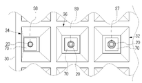
図1Aは実施形態1に係る発光装置の模式的平面図である。図1Bは、複数の第1包囲部32の位置を理解しやすいよう、図1Aにおいて複数の第1包囲部32を灰色着色部で表示した図である。図1Cは、複数の第2包囲部34の位置を理解しやすいよう、図1Aにおいて複数の第2包囲部34を灰色着色部で表示した図である。図1A、図1B、及び図1Cでは、リフレクタ30の形状を理解しやすいよう、基体10、反射部材70、発光素子22、リフレクタ30のみを図示し、光学部材40などの図示は省略している。図1Dは図1A中の1D-1D断面図であり、図1Eは図1Dの部分拡大図である。図1Fは図1Eの部分拡大図である。
[
1A is a schematic plan view of a light emitting device according to
図1Aから図1Fに示すように、実施形態1に係る発光装置1は、基体10と、基体10の上面に配置される導体配線50と、基体10の上面と導体配線50の上面とを被覆し、基体10の上面の一部と導体配線50の上面の一部とが位置する複数の開口領域を備える反射部材70と、複数の開口領域に位置する導体配線50の一部の上面に接合部材60を介して接合される複数の光源20と、反射部材70上に配置され、平面視で複数の光源20の各々をそれぞれが包囲する複数の包囲部を有し、複数の包囲部のそれぞれが上方に向かって広がる傾斜側面Xを有するリフレクタ30と、を備え、複数の包囲部は、複数の第1包囲部32と、複数の第1包囲部32を取り囲む複数の第2包囲部34とを有し、平面視において、第2包囲部34内における開口領域S8の面積は、第1包囲部32内における開口領域S7の面積よりも小さい発光装置である。以下、詳細に説明する。
As shown in FIGS. 1A to 1F, the
(発光装置1)
発光装置1は例えば直下型バックライト装置である。
(Light emitting device 1)
The
(基体10)
基体10は、光源20を載置するための部材である。
(Substrate 10)
The
基体10の材料としては、例えば、セラミックス、フェノール樹脂、エポキシ樹脂、ポリイミド樹脂、BTレジン、ポリフタルアミド(PPA)、ポリエチレンテレフタレート(PET)等の樹脂が挙げられる。セラミックスとしては、例えば、アルミナ、ムライト、フォルステライト、ガラスセラミックス、窒化物系(例えば、AlN)、炭化物系(例えば、SiC)、LTCC等が挙げられる。基体10の材料に樹脂を用いる場合は、ガラス繊維や、SiO2、TiO2、Al2O3等の無機フィラーを樹脂に混合し、機械的強度の向上、熱膨張率の低減、光反射率の向上等を図ることもできる。基体10には、金属部材の表面に絶縁層が形成された金属基板を用いてもよい。
Materials for the
基体10の厚さは適宜選択することができる。基体10は、例えば、ロール・ツー・ロール方式で製造可能なフレキシブル基板であってもよいし、リジット基板であってもよい。リジット基板は湾曲可能な薄型リジット基板であってもよい。
The thickness of the
(導体配線50)
基体10の少なくとも上面には、光源20(発光素子22)に電力を供給するための導体配線50を配置することができる。導体配線50は、光源20(発光素子22)の電極と電気的に接続され、外部からの電流(電力)を供給するための部材である。
(Conductor wiring 50)
A
導体配線50の材料は、基体10として用いられる材料や製造方法等によって適宜選択することができる。例えば、基体10の材料としてセラミックスを用いる場合、導体配線50の材料には、セラミックスシートの焼成温度にも耐え得る高融点を有する材料を用いるのが好ましく、例えば、タングステン、モリブデンのような高融点の金属を用いるのが好ましい。さらに、これらの金属の表面を、鍍金やスパッタリング、蒸着などにより、ニッケル、金、銀などの他の金属材料で被覆したものを導体配線50として用いることもできる。基体10の材料としてガラスエポキシ樹脂を用いる場合、導体配線50の材料には、加工し易い材料を用いることが好ましい。
The material of the
導体配線50は、基体10の一面又は両面に、蒸着、スパッタ、めっき等の方法によって形成することができる。プレスにより金属箔を貼りつけてこれを導体配線50としてもよい。印刷法又はフォトリソグラフィー等を用いてマスキングし、エッチング工程によって、所定の形状に導体配線50をパターニングすることができる。
The
(反射部材70)
反射部材70は、光を反射させ、あるいは光の漏れや吸収を防いで、発光装置1の光取り出し効率を上げる絶縁性の部材である。反射部材70は、基体10の上面と導体配線50の上面とを被覆するよう配置される。反射部材70には、例えば白色系のフィラーを含有する部材を用いることができる。反射部材70の材料は、絶縁性であれば特に限定されないが、発光素子22からの光の吸収が少ない材料であることが特に好ましい。具体的には、例えば、エポキシ、シリコーン、変性シリコーン、ウレタン樹脂、オキセタン樹脂、アクリル、ポリカーボネイト、ポリイミド等を反射部材70の材料として用いることができる。
(Reflection member 70)
The reflecting
反射部材70は、基体10の上面の一部と導体配線50の上面の一部とが位置する複数の開口領域S7、S8を備えており、例えば図4A、図4Bに示すように、平面視において、第2包囲部34内における開口領域S8の面積は、第1包囲部32内における開口領域S7の面積よりも小さい。このようにすれば、第2包囲部34内においては、第1包囲部32内におけるよりも、多くの光が反射部材70で反射されるものとなって、装置外周部における包囲部上の光密度が、装置中央部における包囲部上の光密度よりも高くなる。したがって、装置外周部上において装置中央部上と同等の輝度を確保して、装置上の輝度を装置の全域において均一に近づけることができる。
The reflecting
(複数の光源20)
複数の光源20は、複数の開口領域S7、S8に位置する導体配線50の一部の上面に接合部材60を介して接合される。
(plurality of light sources 20)
A plurality of
複数の光源20のピッチ、つまり、複数の光源20が隣接する間隔Pは、平面視における縦方向及び横方向において均一(均一であるとみなせる程度の誤差がある場合を含む。)であることが好ましい。本実施形態によれば、第2包囲部34における開口領域S8の面積が第1包囲部32における開口面積S7よりも小さいものとされるため、光源20の配置等に変更を加えるなどの比較的煩雑な設計を行わずとも、装置外周部上の輝度を装置中央部上と同等に確保することが可能となり、発光装置1の設計が容易になる。反射部材70が有する開口面積S7、S8の大きさを変えることに加えて、さらにリフレクタ30における第1包囲部32と第2包囲部34の大きさを変えるものとすれば、例えば、第2包囲部34の傾斜側面Xの上端で規定される上端開口面積S2を、第1包囲部32の傾斜側面Xの上端で規定される上端開口面積S1よりも小さいものとすれば、より一層、装置外周部上の輝度を装置中央部上と同等に確保することが容易になる。したがって、光源20の配置等に変更を加える必要性がさらに低下し、発光装置1の設計の自由度をより容易に確保することができる。
The pitch of the plurality of
各光源20は発光ダイオードなどの発光素子22を有していてもよい。発光素子22は、例えば、透光性の基板と、基板上に積層された半導体層と、を有する。透光性の基板には、例えばサファイアを用いることができる。半導体層は、例えば、n型半導体層、活性層、及びp型半導体層を、基板側からこの順に有している。半導体層には、例えば、ZnSe、窒化物系半導体(InxAlyGa1-x-yN、0≦X、0≦Y、X+Y≦1)、またはGaPなどのほか、GaAlAs、AlInGaPなどを用いることができる。n型半導体層上には例えばn側電極が形成されており、p型半導体層上には例えばp側電極が形成されている。
Each
各光源20は封止部材26を有していてもよい。封止部材26は、発光素子22を外部環境から保護するとともに、発光素子22から出力される光を光学的に制御する部材である。封止部材26は、発光素子22を被覆するように基体10上に配置される。平面視において、反射部材70が有する開口領域S7、S8の光源側端部は、封止部材26の内側に位置していてもよいし、外側に位置してもよい。光源側端部が封止部材26の内側に位置する場合、開口領域S7、S8は封止部材26に覆われるものとなるが、封止部材26の外側に位置する場合は、開口領域S7、S8内に封止部材70が配置されるものとなる。
Each
封止部材26の材料としては、エポキシ樹脂やシリコーン樹脂あるいはそれらを混合させた樹脂や、ガラスなどの透光性材料を用いることができる。これらのうち、耐光性および成形のしやすさを考慮して、シリコーン樹脂を選択することが好ましい。封止部材26には、光拡散材や、発光素子22からの光を吸収して発光素子22からの出力光とは異なる波長の光を発する蛍光体等の波長変換部材や、発光素子22の発光色に対応する着色剤を含有させることができる。
As a material of the sealing
封止部材26は、例えば、圧縮成型や射出成型などのほか、滴下や描画により形成することができる。また、封止部材26の材料の粘度を最適化することにより、材料自体の表面張力によって形状を制御することも可能である。滴下や描画による場合は、金型を必要とすることなく、より簡便に封止部材26を形成することができる。粘度は、所望の粘度を有する材料を封止部材26の材料として用いることにより調整してもよいし、上述した光拡散材、波長変換部材、あるいは着色剤を利用して調整してもよい。
The sealing
各光源20はバットウィング型の配光特性を有していることが好ましい。このようにすれば、各光源20の真上方向に出射される光量を抑制して、各光源20の配光を広げることができる。したがって、特に基体10と対向して透光性の光学部材40を設ける場合において、発光装置1の厚みを小さくすることができる。よって、装置外周部上において装置中央部上と同等の輝度を確保しつつ、厚みが小さい薄型の発光装置を提供することができる。
Each
バットウィング型の配光特性とは、中心部が外周部よりも暗くなる配光特性をいう。バットウィング型の配光特性の一例としては、光軸Lを0°とする場合に、0°よりも配光角の絶対値が大きい角度において、発光強度が強くなる発光強度分布を有する配光特性や、45°~90°付近において、発光強度が最も強くなる発光強度分布を有する配向特性を挙げることができる。 A batwing type light distribution characteristic is a light distribution characteristic in which the central portion is darker than the outer peripheral portion. As an example of the batwing type light distribution characteristic, when the optical axis L is 0°, the light distribution has a light emission intensity distribution in which the light emission intensity increases at angles where the absolute value of the light distribution angle is larger than 0°. Orientation characteristics having an emission intensity distribution in which the emission intensity becomes the strongest in the vicinity of 45° to 90°.
各光源20は、発光素子22の上面に反射層28を有していてもよい。この場合、封止部材26は、例えば発光素子22と反射層28とを被覆するように設けることができる。このように封止部材26を設ければ、封止部材26を例えば後述する図2Aに示す形状などのような形状に形成して、バットウィング型の配光特性を容易に実現することができる。
Each
図2Aは実施形態1に係る光源の他の例を示す模式的断面図である。封止部材26の形状は例えばドーム状であってもよいが、図2Aに示すように、発光素子22からの光を広配光化させる形状、具体的には、発光素子の直上に凹部を有する形状であってもよい。このようにすれば、封止部材26が広配光化させるレンズとして機能し、前述した反射層28を設けずとも、バットウィング型の配光特性を得ることが可能となる。あるいは、反射層28を設けつつレンズとして機能する封止部材26を設けることで、さらに容易にバットウィング型の配光特性を得ることが可能となる。
2A is a schematic cross-sectional view showing another example of the light source according to
図2Bは実施形態1に係る光源の他の例を示す模式的断面図である。図2Bに示すように、各光源20は封止部材26の上方に反射層28を有していてもよい。このようにすれば、発光素子22の上方向への光は反射層28で反射され、発光素子22の直上の光量が抑制される。したがって、バットウィング型の配光特性を容易に実現することができる。
2B is a schematic cross-sectional view showing another example of the light source according to
反射層28は、金属膜であってもよいし、誘電体多層膜であってもよい。
The
複数の光源20は、互いに独立して駆動可能であることが好ましく、特に、光源20ごとの調光制御(例えば、ローカルディミングやハイダイナミックレンジ:HDR)が可能であることが好ましい。
It is preferable that the plurality of
(リフレクタ30)
リフレクタ30は、光源20から出射される光を反射する部材である。リフレクタ30は、光源20からの出射光に対する反射率が、440nm~630nmの領域で平均70%以上であることが好ましい。リフレクタ30には、例えば、酸化チタン、酸化アルミニウム、酸化ケイ素等の金属酸化物粒子からなる反射材を含有する樹脂を用いて成形された部材や、反射材を含有しない樹脂の表面に反射材が設けられた部材などを用いることができる。
(Reflector 30)
The
リフレクタ30は、反射部材70上に配置され、平面視で複数の光源20の各々をそれぞれが包囲する複数の包囲部を有する。1つの包囲部は1つの光源を包囲する。複数の包囲部は、複数の第1包囲部32と、複数の第1包囲部32を取り囲む複数の第2包囲部34と、を有する。複数の包囲部それぞれは、上方に向かって広がる傾斜側面Xを有する。ここで、第2包囲部34の傾斜側面Xの上端で規定される上端開口面積S2は、第1包囲部32の傾斜側面Xの上端で規定される上端開口面積S1よりも小さいことが好ましい。このようにすれば、より一層、第2包囲部34上の光密度が第1包囲部32上の光密度よりも高くなり、すなわち、装置外周部上の光密度が装置中央部上の光密度よりも高くなり、装置外周部上の輝度を装置中央部上と同等に確保することが容易になる。なお、光密度とは単位面積当たりの光の強さの度合いである。
The
リフレクタ30の厚みTは、例えば100~300μmである。
The thickness T of the
ここで、リフレクタ30は、さらに、複数の包囲部それぞれにおいて、傾斜側面Xの下端から光源20に向かって延在する平面部を有することが好ましい。なお、図1Eでは、第2包囲部34の傾斜側面Xの傾斜角度が、第1包囲部32の傾斜側面Xの傾斜角度よりも大きい。
Here, it is preferable that the
例えば図4Bに示すように、第2包囲部34における平面部の光源側端部から光源端部までの距離D2は、第1包囲部32における平面部の光源側端部から光源端部までの距離D1よりも小さいことが好ましい。このようにすれば、より一層、第2包囲部34上の光密度を第1包囲部32上の光密度より高くして、装置外周部における包囲部上の光密度を、装置中央部における包囲部上の光密度よりも高くすることができる。したがって、装置外周部上の輝度を装置中央部上と同等に確保することがさらに容易になる。
For example, as shown in FIG. 4B, the distance D2 from the light source end of the planar portion of the
図3は実施形態1に係るリフレクタの他の例を示す模式的断面図である。図3に示すように、基体10の上面から第2包囲部34の傾斜側面Xの上端までの高さH2は、基体10の上面から第1包囲部32の上端までの高さH1より高いことが好ましい。このようにすれば、第2包囲部34内での光の多重反射量が増すため、より一層、第2包囲部34上の光密度を高めて、装置外周部上の輝度を高めることができる。
FIG. 3 is a schematic cross-sectional view showing another example of the reflector according to
(光学部材40)
光学部材40は複数の光源20を挟んで基体10と対向するよう配置される。傾斜側面Xの上端から光学部材40までの距離K2は、基体10上面から傾斜側面Xの上端までの距離K1の1/2以下であることが好ましい。このようにすれば、リフレクタ30から光学部材40までの距離に対して、第1包囲部32や第2包囲部34の深さが相対的に深くなり、第1包囲部32や第2包囲部34内における光の多重反射の繰り返し回数を増やすことができる。したがって、光学部材40が配置されている位置における、各包囲部の光密度を高めることができる。
(Optical member 40)
The
光学部材40には例えばハーフミラーなどの透光性の部材を用いることができる。ハーフミラーには、例えば、入射する光の一部を反射し、一部を透過する部材を用いることができる。
A translucent member such as a half mirror can be used for the
ハーフミラーの反射率は、垂直入射よりも斜め入射の方が低くなるように設定されていることが好ましい。すなわち、ハーフミラーは、各光源20から放射された光のうち、光軸方向に対して平行に出射した光に対しては、光反射率が高く、放射角度(光軸方向に対して平行である場合は放射角度が0度であるものとする。)が広がっていくに従い、光反射率が低下する特性(換言すると、ハーフミラーを透過する光量が増加する特性)を有していることが好ましい。このようにすれば、ハーフミラーを光出射側から観察した場合において、均質な輝度分布を容易に得ることができる。
The reflectance of the half mirror is preferably set to be lower for oblique incidence than for vertical incidence. That is, the half mirror has a high light reflectance for light emitted from each
ハーフミラーには例えば誘電体多層膜を用いることができる。誘電体多層膜を用いることで、光吸収の少ない反射膜を得ることができる。加えて、膜の設計により反射率を任意に調整することができ、角度によって反射率を制御することも可能となる。例えば、ハーフミラーに対して垂直に入射する光に対してこれよりも斜めに入射する光に対して反射率が低くなるよう誘電体多層膜の膜を設計すれば、光取り出し面に対して垂直に入射する光に対する反射率が高く、光取り出し面に対する角度が大きくなるほど反射率が低くなる特性を容易に実現することができる。 A dielectric multilayer film, for example, can be used for the half mirror. By using a dielectric multilayer film, a reflective film with little light absorption can be obtained. In addition, the reflectance can be arbitrarily adjusted by film design, and the reflectance can be controlled by the angle. For example, if the dielectric multilayer film is designed so that the reflectance of light incident obliquely to the half mirror is lower than that of light incident perpendicular to the half mirror, It is possible to easily realize a characteristic in which the reflectance for light incident on the light-extracting surface is high, and the reflectance decreases as the angle to the light extraction surface increases.
発光装置1は、光学部材40の光出射側に光拡散板を備えていてもよい。光拡散板は、複数の光源20から放射された光を拡散させることにより輝度ムラを削減させる部材である。光拡散板を形成する材料には、例えば、ポリカーボネイト樹脂、ポリスチレン樹脂、アクリル樹脂、ポリエチレン樹脂等、可視光に対して光吸収の少ない材料を用いることができる。光拡散板には、例えば、母材となる材料中に屈折率の異なる材料を含有させた部材や、母材となる材料の表面形状を加工して光を散乱させる部材を用いることができる。
The
(接合部材60)
発光装置1は接合部材60を有している。接合部材60は、光源20を基体10及び/又は導体配線50に固定するための部材である。接合部材60の一例としては、絶縁性の樹脂や導電性の部材が挙げられる。光源20をフリップチップ実装する場合は導電性の部材を接合部材60として用いることができる。Au含有合金、Ag含有合金、Pd含有合金、In含有合金、Pb-Pd含有合金、Au-Ga含有合金、Au-Sn含有合金、Sn含有合金、Sn-Cu含有合金、Sn-Cu-Ag含有合金、Au-Ge含有合金、Au-Si含有合金、Al含有合金、Cu-In含有合金、金属とフラックスの混合物等は接合部材60の一例である。
(joining member 60)
The
接合部材60としては、例えば、液状、ペースト状、固体状(シート状、ブロック状、粉末状、ワイヤ状)の部材を単一にまたは組み合わせて用いることができ、組成や基体10の形状等に応じて、適宜選択することができる。光源20を導体配線50に電気的に接続する工程と、光源20を基体10上に載置や固定などする工程と、を一の工程ではなく別の工程に分けて行う場合には、接合部材60とは別のワイヤをさらに用いて、これで光源と導体配線50を電気的に接続してもよい。
As the
以上説明したように、実施形態1に係る発光装置1によれば、平面視において、第2包囲部34内における開口領域S8の面積が、第1包囲部32内における開口領域S7の面積よりも小さい。このため、第2包囲部34内においては、第1包囲部32内におけるよりも、多くの光が反射部材70で反射されるものとなり、装置外周部における包囲部上の光密度が、装置中央部における包囲部上の光密度よりも高くなる。したがって、装置外周部上において装置中央部上と同等の輝度を確保して、装置上の輝度を装置の全域において均一に近づけることができる。
As described above, according to the
[実施形態2に係る発光装置2]
図5Aは実施形態2に係る発光装置の模式的平面図であり、図5Bは、複数の第1包囲部32の位置を理解しやすいよう、図5Aにおいて複数の第1包囲部32を灰色着色部で表示した図である。図5Cは、複数の第2包囲部34の位置を理解しやすいよう、図5Aにおいて複数の第2包囲部34を灰色着色部で表示した図である。図5Dは、複数の第3包囲部36の位置を理解しやすいよう、図5Aにおいて複数の第3包囲部36を灰色着色部で表示した図である。図5Eは図5A中の5E-5E断面図である。図5Fは図5Aの部分拡大図において第1包囲部と第2包囲部と第3包囲部とにおける反射部材の開口領域をそれぞれ灰色着色部で表示した図である。
[Light-emitting device 2 according to Embodiment 2]
FIG. 5A is a schematic plan view of a light emitting device according to Embodiment 2, and FIG. 5B shows a plurality of first surrounding
図5Aから図5Fに示すように、実施形態2に係る発光装置2は、複数の包囲部が、第1包囲部32と第2包囲部34との間に複数の第3包囲部36を有しており、平面視において、第3包囲部36内における開口領域S9の面積は、第1包囲部32内における開口領域S7の面積よりも小さく、第2包囲部34内における開口領域S8の面積よりも大きい点で、実施形態1に係る発光装置1と相違する。実施形態2に係る発光装置2によれば、第2包囲部34上の光密度>第3包囲部36上の光密度>第1包囲部32上の光密度の関係が成立し、装置中央部から装置外周部に向かうにつれて、装置上の光密度が高くなる。したがって、装置外周部上において装置中央部上と同等の輝度を確保して、装置上の輝度を装置の全域において均一に近づけることができる。なお、各第3包囲部36における傾斜側面Xの上端で規定される開口面積S3は、第1包囲部32の開口面積S1よりも小さく、第2包囲部34の開口面積S2よりも大きいことが好ましい。このようにすれば、上記の光密度の関係を成立させることがさらに容易となり、より一層、装置外周部上において装置中央部上と同等の輝度を確保して、装置上の輝度を装置の全域において均一に近づけることができる。
As shown in FIGS. 5A to 5F, in the light emitting device 2 according to the second embodiment, the plurality of enclosing portions has a plurality of
以上、実施形態について説明したが、これらの説明によって特許請求の範囲に記載された構成は何ら限定されるものではない。 Although the embodiments have been described above, the configurations described in the claims are not limited by these descriptions.
1 発光装置
10 基体
20 光源
22 発光素子
26 封止部材
28 反射層
30 リフレクタ
32 第1包囲部
34 第2包囲部
36 第3包囲部
40 光学部材
50 導体配線
60 接合部材
70 反射部材
D1、D2 包囲部における平面部の光源側端部から光源端部までの距離
H1、H2 基体の上面から傾斜側面の上端までの高さ
K1 基体上面から傾斜側面の上端までの距離
K2 傾斜側面の上端から光学部材までの距離
P 光源が隣接する間隔(ピッチ)
S1、S2、S3 包囲部の開口面積
S7、S8、S9 反射部材が有する開口領域の面積
T リフレクタの厚み
X 傾斜側面
1
S1, S2, S3 Opening area of the surrounding part S7, S8, S9 Area of the opening area of the reflecting member T Reflector thickness X Inclined side surface
Claims (13)
前記基体の上面に配置される導体配線と、
前記基体の上面と前記導体配線の上面とを被覆し、前記基体の上面の一部と前記導体配線の上面の一部とが位置する複数の開口領域を備える反射部材と、
前記複数の開口領域に位置する前記導体配線の一部の上面に接合部材を介して接合される複数の光源と、
前記反射部材上に配置され、平面視で前記複数の光源の各々をそれぞれが包囲する複数の包囲部を有し、前記複数の包囲部のそれぞれが上方に向かって広がる傾斜側面を有するリフレクタと、を備え、
前記複数の包囲部は、複数の第1包囲部と、前記複数の第1包囲部を取り囲む複数の第2包囲部とを有し、
平面視において、個々の前記第2包囲部内における前記開口領域の面積は、いずれの前記第1包囲部内における前記開口領域の面積よりも小さい発光装置。 a substrate;
a conductor wiring arranged on the upper surface of the base;
a reflective member that covers the top surface of the base and the top surface of the conductor wiring, and has a plurality of opening regions where a part of the top surface of the base and a part of the top surface of the conductor wiring are located;
a plurality of light sources bonded via a bonding member to the upper surface of a portion of the conductor wiring located in the plurality of opening regions;
a reflector disposed on the reflecting member and having a plurality of enclosing portions that enclose each of the plurality of light sources in plan view, each of the plurality of enclosing portions having an inclined side surface that spreads upward; with
The plurality of surrounding portions have a plurality of first surrounding portions and a plurality of second surrounding portions surrounding the plurality of first surrounding portions,
The light-emitting device, wherein the area of the opening region in each of the second enclosing portions is smaller than the area of the opening region in any one of the first enclosing portions in plan view.
平面視において、前記第3包囲部内における前記開口領域の面積は、前記第1包囲部内における前記開口領域の面積よりも小さく、前記第2包囲部内における前記開口領域の面積よりも大きい、
請求項1から3のいずれかに記載の発光装置。 The plurality of surrounding portions further includes a plurality of third surrounding portions provided between the first surrounding portion and the second surrounding portion,
In plan view, the area of the opening region within the third enclosing portion is smaller than the area of the opening region within the first enclosing portion and larger than the area of the opening region within the second enclosing portion,
The light-emitting device according to any one of claims 1 to 3.
前記傾斜側面の上端から前記光学部材までの距離は、前記基体上面から前記傾斜側面の上端までの距離の1/2以下である請求項1から9のいずれか1項に記載の発光装置。 A translucent optical member arranged to face the base with the plurality of light sources interposed therebetween;
The light emitting device according to any one of claims 1 to 9, wherein the distance from the upper end of the inclined side surface to the optical member is half or less of the distance from the upper surface of the base to the upper end of the inclined side surface.
前記第2包囲部における前記平面部の前記光源側端部から光源端部までの距離は、前記第1包囲部における前記平面部の前記光源側端部から前記光源端部までの距離よりも小さい請求項1から11のいずれか1項に記載の発光装置。 The reflector has a planar portion extending from a lower end of the inclined side surface toward the light source,
The distance from the light source side end of the flat portion in the second enclosing portion to the light source end is greater than the distance from the light source side end of the flat portion in the first enclosing portion to the light source end. 12. The light emitting device according to any one of claims 1 to 11, wherein .
Priority Applications (3)
| Application Number | Priority Date | Filing Date | Title |
|---|---|---|---|
| JP2018124179A JP7177331B2 (en) | 2018-06-29 | 2018-06-29 | light emitting device |
| US16/457,412 US10903193B2 (en) | 2018-06-29 | 2019-06-28 | Light-emitting device |
| US17/125,408 US11646298B2 (en) | 2018-06-29 | 2020-12-17 | Light-emitting device |
Applications Claiming Priority (1)
| Application Number | Priority Date | Filing Date | Title |
|---|---|---|---|
| JP2018124179A JP7177331B2 (en) | 2018-06-29 | 2018-06-29 | light emitting device |
Publications (2)
| Publication Number | Publication Date |
|---|---|
| JP2020004895A JP2020004895A (en) | 2020-01-09 |
| JP7177331B2 true JP7177331B2 (en) | 2022-11-24 |
Family
ID=69008390
Family Applications (1)
| Application Number | Title | Priority Date | Filing Date |
|---|---|---|---|
| JP2018124179A Active JP7177331B2 (en) | 2018-06-29 | 2018-06-29 | light emitting device |
Country Status (2)
| Country | Link |
|---|---|
| US (2) | US10903193B2 (en) |
| JP (1) | JP7177331B2 (en) |
Families Citing this family (21)
| Publication number | Priority date | Publication date | Assignee | Title |
|---|---|---|---|---|
| KR102631105B1 (en) | 2017-08-31 | 2024-01-30 | 니치아 카가쿠 고교 가부시키가이샤 | Light emitting device |
| JP7177331B2 (en) * | 2018-06-29 | 2022-11-24 | 日亜化学工業株式会社 | light emitting device |
| US11302248B2 (en) | 2019-01-29 | 2022-04-12 | Osram Opto Semiconductors Gmbh | U-led, u-led device, display and method for the same |
| US11156759B2 (en) | 2019-01-29 | 2021-10-26 | Osram Opto Semiconductors Gmbh | μ-LED, μ-LED device, display and method for the same |
| JP7558175B2 (en) | 2019-01-29 | 2024-09-30 | エイエムエス-オスラム インターナショナル ゲーエムベーハー | Video wall, driver circuit, drive control circuit and related methods |
| US11271143B2 (en) | 2019-01-29 | 2022-03-08 | Osram Opto Semiconductors Gmbh | μ-LED, μ-LED device, display and method for the same |
| US11610868B2 (en) | 2019-01-29 | 2023-03-21 | Osram Opto Semiconductors Gmbh | μ-LED, μ-LED device, display and method for the same |
| US12261256B2 (en) | 2019-02-11 | 2025-03-25 | Osram Opto Semiconductors Gmbh | Optoelectronic component, optoelectronic arrangement and method |
| US11538852B2 (en) | 2019-04-23 | 2022-12-27 | Osram Opto Semiconductors Gmbh | μ-LED, μ-LED device, display and method for the same |
| KR20260016601A (en) | 2019-04-23 | 2026-02-03 | 에이엠에스-오스람 인터내셔널 게엠베하 | Led module, led display module and method for producing same |
| CN114303236A (en) | 2019-05-13 | 2022-04-08 | 奥斯兰姆奥普托半导体股份有限两合公司 | Multi-chip bearing structure |
| CN114144727A (en) | 2019-05-23 | 2022-03-04 | 奥斯兰姆奥普托半导体股份有限两合公司 | Lighting device, light guide device and method |
| US11804580B2 (en) * | 2019-11-04 | 2023-10-31 | Sharp Kabushiki Kaisha | Lighting device and method of producing light source substrate |
| JP7332895B2 (en) * | 2020-01-31 | 2023-08-24 | 日亜化学工業株式会社 | Method for manufacturing planar light source, planar light source, and light source |
| CN111352274A (en) * | 2020-03-18 | 2020-06-30 | 深圳市隆利科技股份有限公司 | Method and device for preparing flexible direct type backlight module |
| JP7144694B2 (en) * | 2020-07-31 | 2022-09-30 | 日亜化学工業株式会社 | Light emitting module, planar light source, liquid crystal display device |
| CN114578614B (en) * | 2020-11-30 | 2025-01-03 | 华为技术有限公司 | Backlight module and display screen |
| WO2023039855A1 (en) * | 2021-09-17 | 2023-03-23 | 瑞仪(广州)光电子器件有限公司 | Reflector sheet, backlight module and display apparatus |
| JP2023077024A (en) | 2021-11-24 | 2023-06-05 | 日亜化学工業株式会社 | planar light source |
| WO2024002827A1 (en) * | 2022-06-28 | 2024-01-04 | Signify Holding B.V. | An insert for a light emitting device |
| CN116974109B (en) * | 2023-08-01 | 2026-01-16 | 上海天马微电子有限公司 | Direct-lit backlight module, backlight module design method and display device |
Citations (8)
| Publication number | Priority date | Publication date | Assignee | Title |
|---|---|---|---|---|
| JP2001257381A (en) | 2000-03-13 | 2001-09-21 | Sharp Corp | Light emitting diode, method of manufacturing the same, and lighting device |
| JP2006013265A (en) | 2004-06-28 | 2006-01-12 | Kyocera Corp | LIGHT EMITTING DEVICE AND LIGHTING DEVICE USING THE SAME |
| JP2010123570A (en) | 2008-10-22 | 2010-06-03 | Toshiba Lighting & Technology Corp | Luminaire |
| WO2012005061A1 (en) | 2010-07-07 | 2012-01-12 | シャープ株式会社 | Backlight unit |
| JP2012248769A (en) | 2011-05-30 | 2012-12-13 | Sharp Corp | Light-emitting device and display device |
| US20130051017A1 (en) | 2011-02-23 | 2013-02-28 | The Sloan Company, Inc. Dba Sloanled | Led based down light |
| JP2013149711A (en) | 2012-01-18 | 2013-08-01 | Citizen Holdings Co Ltd | Semiconductor light-emitting device |
| JP2018045972A (en) | 2016-09-16 | 2018-03-22 | 日亜化学工業株式会社 | Light emitting device |
Family Cites Families (20)
| Publication number | Priority date | Publication date | Assignee | Title |
|---|---|---|---|---|
| US8080828B2 (en) | 2006-06-09 | 2011-12-20 | Philips Lumileds Lighting Company, Llc | Low profile side emitting LED with window layer and phosphor layer |
| EP1895602B1 (en) | 2006-08-29 | 2019-01-23 | Toshiba Lighting & Technology Corporation | Illumination apparatus having a plurality of semiconductor light-emitting devices |
| JP2011181219A (en) | 2010-02-26 | 2011-09-15 | Toshiba Corp | Light source, surface light source module, and method of manufacturing the light source |
| WO2012023459A1 (en) | 2010-08-20 | 2012-02-23 | シャープ株式会社 | Illuminating device, display device and television receiver |
| US20120147589A1 (en) | 2010-12-14 | 2012-06-14 | Todd Farmer | System for Providing a Directional LED Array |
| US9882094B2 (en) | 2011-03-14 | 2018-01-30 | Intellectual Discovery Co., Ltd. | Light source with inner and outer bodies comprising three different encapsulants |
| EP2704221A4 (en) | 2011-04-28 | 2014-10-15 | Asahi Rubber Inc | SEMICONDUCTOR LENS DEVICE AND METHOD FOR MANUFACTURING THE SAME |
| US9228715B2 (en) | 2012-02-22 | 2016-01-05 | Avago Technologies General Ip (Singapore) Pte. Ltd. | Hybrid canopy lighting for optimum light beam shaping |
| US9874322B2 (en) | 2012-04-10 | 2018-01-23 | Cree, Inc. | Lensed troffer-style light fixture |
| JP5999983B2 (en) | 2012-05-28 | 2016-09-28 | シャープ株式会社 | Illumination device and display device |
| JP2013247092A (en) | 2012-05-29 | 2013-12-09 | Sharp Corp | Light-emitting device, lighting device, and display device |
| ES2435501B1 (en) | 2013-10-21 | 2014-05-28 | Simon, S.A.U. | LUMINARY |
| KR102319111B1 (en) | 2015-03-30 | 2021-11-01 | 삼성디스플레이 주식회사 | Light emitting device |
| JP6506899B2 (en) | 2015-10-08 | 2019-04-24 | 日亜化学工業株式会社 | Light emitting device, integrated light emitting device and light emitting module |
| WO2017061127A1 (en) | 2015-10-08 | 2017-04-13 | Nichia Corporation | Light-emitting device, integrated light-emitting device, and light-emitting module |
| JP6299811B2 (en) | 2015-11-04 | 2018-03-28 | 日亜化学工業株式会社 | Light emitting device |
| US10274168B2 (en) * | 2016-07-20 | 2019-04-30 | Nichia Corporation | Light emitting device |
| JP6868388B2 (en) * | 2016-12-26 | 2021-05-12 | 日亜化学工業株式会社 | Light emitting device and integrated light emitting device |
| KR102631105B1 (en) * | 2017-08-31 | 2024-01-30 | 니치아 카가쿠 고교 가부시키가이샤 | Light emitting device |
| JP7177331B2 (en) * | 2018-06-29 | 2022-11-24 | 日亜化学工業株式会社 | light emitting device |
-
2018
- 2018-06-29 JP JP2018124179A patent/JP7177331B2/en active Active
-
2019
- 2019-06-28 US US16/457,412 patent/US10903193B2/en active Active
-
2020
- 2020-12-17 US US17/125,408 patent/US11646298B2/en active Active
Patent Citations (8)
| Publication number | Priority date | Publication date | Assignee | Title |
|---|---|---|---|---|
| JP2001257381A (en) | 2000-03-13 | 2001-09-21 | Sharp Corp | Light emitting diode, method of manufacturing the same, and lighting device |
| JP2006013265A (en) | 2004-06-28 | 2006-01-12 | Kyocera Corp | LIGHT EMITTING DEVICE AND LIGHTING DEVICE USING THE SAME |
| JP2010123570A (en) | 2008-10-22 | 2010-06-03 | Toshiba Lighting & Technology Corp | Luminaire |
| WO2012005061A1 (en) | 2010-07-07 | 2012-01-12 | シャープ株式会社 | Backlight unit |
| US20130051017A1 (en) | 2011-02-23 | 2013-02-28 | The Sloan Company, Inc. Dba Sloanled | Led based down light |
| JP2012248769A (en) | 2011-05-30 | 2012-12-13 | Sharp Corp | Light-emitting device and display device |
| JP2013149711A (en) | 2012-01-18 | 2013-08-01 | Citizen Holdings Co Ltd | Semiconductor light-emitting device |
| JP2018045972A (en) | 2016-09-16 | 2018-03-22 | 日亜化学工業株式会社 | Light emitting device |
Also Published As
| Publication number | Publication date |
|---|---|
| US20200006297A1 (en) | 2020-01-02 |
| US10903193B2 (en) | 2021-01-26 |
| US11646298B2 (en) | 2023-05-09 |
| US20210104502A1 (en) | 2021-04-08 |
| JP2020004895A (en) | 2020-01-09 |
Similar Documents
| Publication | Publication Date | Title |
|---|---|---|
| JP7177331B2 (en) | light emitting device | |
| JP7381974B2 (en) | light emitting device | |
| JP7125636B2 (en) | light emitting device | |
| JP7522529B2 (en) | Light-emitting device | |
| JP6493345B2 (en) | Light emitting device | |
| RU2717381C2 (en) | Light-emitting device, integrated light-emitting device and light-emitting module | |
| JP2018107279A (en) | Light-emitting device and integration type light-emitting device | |
| JP2006066657A (en) | Light emitting device and lighting device | |
| JP6575507B2 (en) | Light emitting device and integrated light emitting device | |
| JP7014966B2 (en) | Luminescent device | |
| JP4938255B2 (en) | Light emitting element storage package, light source, and light emitting device | |
| JP4557613B2 (en) | Light emitting element storage package, light emitting device, and lighting device | |
| JP7144683B2 (en) | light emitting device | |
| JP2005310911A (en) | Light emitting element storage package, light emitting device, and lighting device | |
| JP4659515B2 (en) | Light-emitting element mounting substrate, light-emitting element storage package, light-emitting device, and lighting device | |
| JP7189464B2 (en) | light emitting device | |
| JP6923832B2 (en) | Light emitting device | |
| JP7212296B2 (en) | light emitting device | |
| JP7144682B2 (en) | light emitting device | |
| JP2019083217A (en) | Light emitting device |
Legal Events
| Date | Code | Title | Description |
|---|---|---|---|
| A621 | Written request for application examination |
Free format text: JAPANESE INTERMEDIATE CODE: A621 Effective date: 20210603 |
|
| A977 | Report on retrieval |
Free format text: JAPANESE INTERMEDIATE CODE: A971007 Effective date: 20220418 |
|
| A131 | Notification of reasons for refusal |
Free format text: JAPANESE INTERMEDIATE CODE: A131 Effective date: 20220510 |
|
| A521 | Request for written amendment filed |
Free format text: JAPANESE INTERMEDIATE CODE: A523 Effective date: 20220708 |
|
| TRDD | Decision of grant or rejection written | ||
| A01 | Written decision to grant a patent or to grant a registration (utility model) |
Free format text: JAPANESE INTERMEDIATE CODE: A01 Effective date: 20221011 |
|
| A61 | First payment of annual fees (during grant procedure) |
Free format text: JAPANESE INTERMEDIATE CODE: A61 Effective date: 20221024 |
|
| R151 | Written notification of patent or utility model registration |
Ref document number: 7177331 Country of ref document: JP Free format text: JAPANESE INTERMEDIATE CODE: R151 |
|
| R250 | Receipt of annual fees |
Free format text: JAPANESE INTERMEDIATE CODE: R250 |