RU2717381C2 - Light-emitting device, integrated light-emitting device and light-emitting module - Google Patents
Light-emitting device, integrated light-emitting device and light-emitting module Download PDFInfo
- Publication number
- RU2717381C2 RU2717381C2 RU2018112372A RU2018112372A RU2717381C2 RU 2717381 C2 RU2717381 C2 RU 2717381C2 RU 2018112372 A RU2018112372 A RU 2018112372A RU 2018112372 A RU2018112372 A RU 2018112372A RU 2717381 C2 RU2717381 C2 RU 2717381C2
- Authority
- RU
- Russia
- Prior art keywords
- light
- light emitting
- emitting device
- radiation
- emitting element
- Prior art date
Links
Images

Classifications
-
- H—ELECTRICITY
- H01—ELECTRIC ELEMENTS
- H01L—SEMICONDUCTOR DEVICES NOT COVERED BY CLASS H10
- H01L25/00—Assemblies consisting of a plurality of individual semiconductor or other solid state devices ; Multistep manufacturing processes thereof
- H01L25/03—Assemblies consisting of a plurality of individual semiconductor or other solid state devices ; Multistep manufacturing processes thereof all the devices being of a type provided for in the same subgroup of groups H01L27/00 - H01L33/00, or in a single subclass of H10K, H10N, e.g. assemblies of rectifier diodes
- H01L25/04—Assemblies consisting of a plurality of individual semiconductor or other solid state devices ; Multistep manufacturing processes thereof all the devices being of a type provided for in the same subgroup of groups H01L27/00 - H01L33/00, or in a single subclass of H10K, H10N, e.g. assemblies of rectifier diodes the devices not having separate containers
- H01L25/075—Assemblies consisting of a plurality of individual semiconductor or other solid state devices ; Multistep manufacturing processes thereof all the devices being of a type provided for in the same subgroup of groups H01L27/00 - H01L33/00, or in a single subclass of H10K, H10N, e.g. assemblies of rectifier diodes the devices not having separate containers the devices being of a type provided for in group H01L33/00
- H01L25/0753—Assemblies consisting of a plurality of individual semiconductor or other solid state devices ; Multistep manufacturing processes thereof all the devices being of a type provided for in the same subgroup of groups H01L27/00 - H01L33/00, or in a single subclass of H10K, H10N, e.g. assemblies of rectifier diodes the devices not having separate containers the devices being of a type provided for in group H01L33/00 the devices being arranged next to each other
-
- H—ELECTRICITY
- H01—ELECTRIC ELEMENTS
- H01L—SEMICONDUCTOR DEVICES NOT COVERED BY CLASS H10
- H01L33/00—Semiconductor devices with at least one potential-jump barrier or surface barrier specially adapted for light emission; Processes or apparatus specially adapted for the manufacture or treatment thereof or of parts thereof; Details thereof
- H01L33/44—Semiconductor devices with at least one potential-jump barrier or surface barrier specially adapted for light emission; Processes or apparatus specially adapted for the manufacture or treatment thereof or of parts thereof; Details thereof characterised by the coatings, e.g. passivation layer or anti-reflective coating
- H01L33/46—Reflective coating, e.g. dielectric Bragg reflector
-
- H—ELECTRICITY
- H01—ELECTRIC ELEMENTS
- H01L—SEMICONDUCTOR DEVICES NOT COVERED BY CLASS H10
- H01L33/00—Semiconductor devices with at least one potential-jump barrier or surface barrier specially adapted for light emission; Processes or apparatus specially adapted for the manufacture or treatment thereof or of parts thereof; Details thereof
- H01L33/48—Semiconductor devices with at least one potential-jump barrier or surface barrier specially adapted for light emission; Processes or apparatus specially adapted for the manufacture or treatment thereof or of parts thereof; Details thereof characterised by the semiconductor body packages
- H01L33/50—Wavelength conversion elements
- H01L33/505—Wavelength conversion elements characterised by the shape, e.g. plate or foil
-
- H—ELECTRICITY
- H01—ELECTRIC ELEMENTS
- H01L—SEMICONDUCTOR DEVICES NOT COVERED BY CLASS H10
- H01L33/00—Semiconductor devices with at least one potential-jump barrier or surface barrier specially adapted for light emission; Processes or apparatus specially adapted for the manufacture or treatment thereof or of parts thereof; Details thereof
- H01L33/48—Semiconductor devices with at least one potential-jump barrier or surface barrier specially adapted for light emission; Processes or apparatus specially adapted for the manufacture or treatment thereof or of parts thereof; Details thereof characterised by the semiconductor body packages
- H01L33/50—Wavelength conversion elements
- H01L33/507—Wavelength conversion elements the elements being in intimate contact with parts other than the semiconductor body or integrated with parts other than the semiconductor body
-
- H—ELECTRICITY
- H01—ELECTRIC ELEMENTS
- H01L—SEMICONDUCTOR DEVICES NOT COVERED BY CLASS H10
- H01L33/00—Semiconductor devices with at least one potential-jump barrier or surface barrier specially adapted for light emission; Processes or apparatus specially adapted for the manufacture or treatment thereof or of parts thereof; Details thereof
- H01L33/48—Semiconductor devices with at least one potential-jump barrier or surface barrier specially adapted for light emission; Processes or apparatus specially adapted for the manufacture or treatment thereof or of parts thereof; Details thereof characterised by the semiconductor body packages
- H01L33/52—Encapsulations
- H01L33/54—Encapsulations having a particular shape
-
- H—ELECTRICITY
- H01—ELECTRIC ELEMENTS
- H01L—SEMICONDUCTOR DEVICES NOT COVERED BY CLASS H10
- H01L33/00—Semiconductor devices with at least one potential-jump barrier or surface barrier specially adapted for light emission; Processes or apparatus specially adapted for the manufacture or treatment thereof or of parts thereof; Details thereof
- H01L33/48—Semiconductor devices with at least one potential-jump barrier or surface barrier specially adapted for light emission; Processes or apparatus specially adapted for the manufacture or treatment thereof or of parts thereof; Details thereof characterised by the semiconductor body packages
- H01L33/52—Encapsulations
- H01L33/56—Materials, e.g. epoxy or silicone resin
-
- H—ELECTRICITY
- H01—ELECTRIC ELEMENTS
- H01L—SEMICONDUCTOR DEVICES NOT COVERED BY CLASS H10
- H01L33/00—Semiconductor devices with at least one potential-jump barrier or surface barrier specially adapted for light emission; Processes or apparatus specially adapted for the manufacture or treatment thereof or of parts thereof; Details thereof
- H01L33/48—Semiconductor devices with at least one potential-jump barrier or surface barrier specially adapted for light emission; Processes or apparatus specially adapted for the manufacture or treatment thereof or of parts thereof; Details thereof characterised by the semiconductor body packages
- H01L33/58—Optical field-shaping elements
- H01L33/60—Reflective elements
-
- H—ELECTRICITY
- H01—ELECTRIC ELEMENTS
- H01L—SEMICONDUCTOR DEVICES NOT COVERED BY CLASS H10
- H01L33/00—Semiconductor devices with at least one potential-jump barrier or surface barrier specially adapted for light emission; Processes or apparatus specially adapted for the manufacture or treatment thereof or of parts thereof; Details thereof
- H01L33/48—Semiconductor devices with at least one potential-jump barrier or surface barrier specially adapted for light emission; Processes or apparatus specially adapted for the manufacture or treatment thereof or of parts thereof; Details thereof characterised by the semiconductor body packages
- H01L33/62—Arrangements for conducting electric current to or from the semiconductor body, e.g. lead-frames, wire-bonds or solder balls
-
- H—ELECTRICITY
- H01—ELECTRIC ELEMENTS
- H01L—SEMICONDUCTOR DEVICES NOT COVERED BY CLASS H10
- H01L2224/00—Indexing scheme for arrangements for connecting or disconnecting semiconductor or solid-state bodies and methods related thereto as covered by H01L24/00
- H01L2224/01—Means for bonding being attached to, or being formed on, the surface to be connected, e.g. chip-to-package, die-attach, "first-level" interconnects; Manufacturing methods related thereto
- H01L2224/10—Bump connectors; Manufacturing methods related thereto
- H01L2224/15—Structure, shape, material or disposition of the bump connectors after the connecting process
- H01L2224/16—Structure, shape, material or disposition of the bump connectors after the connecting process of an individual bump connector
- H01L2224/161—Disposition
- H01L2224/16151—Disposition the bump connector connecting between a semiconductor or solid-state body and an item not being a semiconductor or solid-state body, e.g. chip-to-substrate, chip-to-passive
- H01L2224/16221—Disposition the bump connector connecting between a semiconductor or solid-state body and an item not being a semiconductor or solid-state body, e.g. chip-to-substrate, chip-to-passive the body and the item being stacked
- H01L2224/16225—Disposition the bump connector connecting between a semiconductor or solid-state body and an item not being a semiconductor or solid-state body, e.g. chip-to-substrate, chip-to-passive the body and the item being stacked the item being non-metallic, e.g. insulating substrate with or without metallisation
-
- H—ELECTRICITY
- H01—ELECTRIC ELEMENTS
- H01L—SEMICONDUCTOR DEVICES NOT COVERED BY CLASS H10
- H01L2924/00—Indexing scheme for arrangements or methods for connecting or disconnecting semiconductor or solid-state bodies as covered by H01L24/00
- H01L2924/10—Details of semiconductor or other solid state devices to be connected
- H01L2924/11—Device type
- H01L2924/12—Passive devices, e.g. 2 terminal devices
- H01L2924/1204—Optical Diode
- H01L2924/12041—LED
-
- H—ELECTRICITY
- H01—ELECTRIC ELEMENTS
- H01L—SEMICONDUCTOR DEVICES NOT COVERED BY CLASS H10
- H01L2924/00—Indexing scheme for arrangements or methods for connecting or disconnecting semiconductor or solid-state bodies as covered by H01L24/00
- H01L2924/15—Details of package parts other than the semiconductor or other solid state devices to be connected
- H01L2924/181—Encapsulation
-
- H—ELECTRICITY
- H01—ELECTRIC ELEMENTS
- H01L—SEMICONDUCTOR DEVICES NOT COVERED BY CLASS H10
- H01L2933/00—Details relating to devices covered by the group H01L33/00 but not provided for in its subgroups
- H01L2933/0008—Processes
- H01L2933/0033—Processes relating to semiconductor body packages
- H01L2933/0058—Processes relating to semiconductor body packages relating to optical field-shaping elements
Abstract
Description
Область техники, к которой относится изобретениеFIELD OF THE INVENTION
Ссылка на родственную заявкуLink to a related application
Эта заявка испрашивает приоритет в соответствии с японской заявкой на патент № 2015-200445 от 08 октября 2015 г., и японской заявкой на патент № 2016-197968 от 06 октября 2016 г., которые полностью включены в этот документ посредством ссылки.This application claims priority in accordance with Japanese Patent Application No. 2015-200445 of October 08, 2015, and Japanese Patent Application No. 2016-197968 of October 6, 2016, which are incorporated herein by reference in their entirety.
Уровень техникиState of the art
Настоящее изобретение относится к светоизлучающим устройствам, интегрированным светоизлучающим устройствам и светоизлучающим модулям.The present invention relates to light emitting devices, integrated light emitting devices, and light emitting modules.
В последние годы были предложены и нашли практическое применение различные электронные компоненты, и необходимо, чтобы они демонстрировали более высокую производительность. В частности, некоторые электронные компоненты должны сохранять свою производительность в течение длительного периода времени в жестких условиях эксплуатации. Такие требования можно применить к светоизлучающим устройствам, в которых используют полупроводниковые светоизлучающие элементы, включая светодиоды (т.е. LED). То есть, в области общего освещения и внутреннего и внешнего освещения для транспортных средств, необходимо, чтобы светоизлучающие устройства изо дня в день демонстрировали более высокую производительность, в частности, более высокую мощность (т.е. более высокую яркость) и более высокую надежность. Более того, требуются светоизлучающие устройства, имеющие низкую стоимость и при этом сохраняющие высокую производительность.In recent years, various electronic components have been proposed and found practical application, and it is necessary that they demonstrate higher performance. In particular, some electronic components must maintain their performance over a long period of time under harsh operating conditions. Such requirements can be applied to light emitting devices that use semiconductor light emitting elements, including LEDs (i.e., LEDs). That is, in the field of general lighting and internal and external lighting for vehicles, it is necessary that the light-emitting devices from day to day show higher performance, in particular, higher power (i.e., higher brightness) and higher reliability. Moreover, light-emitting devices having a low cost and at the same time maintaining high performance are required.
Подсветку, применяемую в жидкокристаллических телевизорах, осветительные устройства общего назначения и т.п. разрабатывают, фокусируясь на их дизайне, что приводит к высокому спросу на их утончение.The backlight used in LCD televisions, general lighting devices, etc. are developed with a focus on their design, which leads to a high demand for their refinement.
Например, в публикации японской заявки на патент № 2008-4948 описано светоизлучающее устройство, в котором отражатель выполнен на верхней поверхности светоизлучающего элемента, установленного на подложке, методом перевернутого кристалла, чтобы таким образом сделать подсветку более тонкой.For example, Japanese Patent Application Publication No. 2008-4948 describes a light-emitting device in which a reflector is formed on an upper surface of a light-emitting element mounted on a substrate by an inverted crystal method to thereby make the backlight thinner.
Публикация японской нерассмотренной заявки на патент № 2008-4948 дает светоизлучающее устройство с широким распределением светового излучения. Однако при дальнейшем утончении подсветки потребовалось светоизлучающее устройство, способное обеспечить гораздо более широкое распределение светового излучения.The publication of Japanese Unexamined Patent Application No. 2008-4948 provides a light emitting device with a wide distribution of light radiation. However, with further refinement of the backlight, a light-emitting device was required, capable of providing a much wider distribution of light radiation.
Сущность изобретенияSUMMARY OF THE INVENTION
Объекты изобретения были разработаны с учетом вышеизложенных обстоятельств, и задача настоящего изобретения заключается в том, чтобы предложить светоизлучающее устройство, которое обеспечивает широкое распределение светового излучения без использования вторичной линзы.The objects of the invention were developed taking into account the above circumstances, and the objective of the present invention is to provide a light emitting device that provides a wide distribution of light radiation without the use of a secondary lens.
Светоизлучающее устройство в соответствии с изобретением включает в себя: основание, содержащее токопроводящие дорожки; светоизлучающий элемент, установленный на основании и приспособленный для испускания светового излучения; светоотражающую пленку, расположенную на верхней поверхности светоизлучающего элемента; и оболочку, покрывающую светоизлучающий элемент и светоотражающую пленку, причем отношение (H/W) высоты (H) оболочки к ширине (W) нижней поверхности оболочки составляет менее 0,5.The light emitting device in accordance with the invention includes: a base comprising conductive paths; a light emitting element mounted on the base and adapted to emit light radiation; a reflective film located on the upper surface of the light emitting element; and a casing covering the light emitting element and the retroreflective film, wherein the ratio (H / W) of the height (H) of the casing to the width (W) of the lower surface of the casing is less than 0.5.
Соответственно, изобретение обеспечивает широкое распределение светового излучения без использования вторичной линзы.Accordingly, the invention provides a wide distribution of light radiation without the use of a secondary lens.
Краткое описание чертежейBrief Description of the Drawings
(Фиг. 1)(Fig. 1)
На фиг. 1 приведен вид в разрезе, показывающий пример светоизлучающего устройства в соответствии с первым вариантом.In FIG. 1 is a sectional view showing an example of a light emitting device in accordance with a first embodiment.
(Фиг. 2)(Fig. 2)
На фиг. 2 приведена диаграмма, показывающая зависимость коэффициента пропускания светового излучения светоотражающей пленки в зависимости от угла падения в этом варианте.In FIG. 2 is a diagram showing the dependence of the transmittance of light radiation of a reflective film as a function of the angle of incidence in this embodiment.
(Фиг. 3)(Fig. 3)
На фиг. 3 приведена диаграмма, показывающая взаимосвязь между диапазоном длин волн светоотражающей пленки и длиной волны излучения светоизлучающего элемента в светоизлучающем устройстве в соответствии с вариантом осуществления изобретения.In FIG. 3 is a diagram showing the relationship between the wavelength range of the reflective film and the radiation wavelength of the light emitting element in the light emitting device in accordance with an embodiment of the invention.
(Фиг. 4)(Fig. 4)
На фиг. 4 показана диаграмма распределения светового излучения светоизлучающего устройства в соответствии с вариантом осуществления изобретения.In FIG. 4 is a light distribution diagram of a light emitting device according to an embodiment of the invention.
(Фиг. 5)(Fig. 5)
На фиг. 5 приведена диаграмма распределения светового излучения светоизлучающего устройства, использующего вторичную линзу, в сравнительном примере.In FIG. 5 is a light distribution diagram of a light emitting device using a secondary lens in a comparative example.
(Фиг. 6)(Fig. 6)
На фиг. 6А-6I показаны экспериментальные примеры в соответствии с вариантом осуществления изобретения.In FIG. 6A-6I show experimental examples in accordance with an embodiment of the invention.
(Фиг. 7)(Fig. 7)
На фиг. 7 приведен вид в поперечном сечении, показывающий пример светоизлучающего модуля во втором варианте осуществления изобретения.In FIG. 7 is a cross-sectional view showing an example of a light emitting module in a second embodiment of the invention.
(Фиг. 8A)(Fig. 8A)
На фиг. 8А показан пример светоотражающей пластины.In FIG. 8A shows an example of a reflective plate.
(Фиг. 8B)(Fig. 8B)
На фиг. 8B показан пример светоотражающей пластины.In FIG. 8B shows an example of a reflective plate.
(Фиг. 9A)(Fig. 9A)
На фиг. 9А показаны характеристики распределения яркости светоизлучающего модуля в соответствии с примером 2.In FIG. 9A shows the luminance distribution characteristics of a light emitting module in accordance with Example 2.
(Фиг. 9B)(Fig. 9B)
На фиг. 9А показаны характеристики распределения яркости светоизлучающего модуля в соответствии с примером 2.In FIG. 9A shows the luminance distribution characteristics of a light emitting module in accordance with Example 2.
Описание вариантов осуществления изобретенияDescription of Embodiments
Варианты осуществления настоящего изобретения будут описаны ниже со ссылкой на прилагаемые чертежи. Светоизлучающее устройство, которое описано ниже, реализует техническую идею настоящего изобретения, и не предполагается, что оно ограничивает настоящее изобретение, если не указано обратное. Содержимое описания касательно одного варианта осуществления или примера также можно применить к другим вариантам осуществления или примерам.Embodiments of the present invention will be described below with reference to the accompanying drawings. The light emitting device, which is described below, implements the technical idea of the present invention, and it is not intended to limit the present invention unless otherwise indicated. The contents of the description regarding one embodiment or example can also be applied to other embodiments or examples.
Более того, в приведенном ниже описании одинаковые названия или ссылочные позиции обозначают одинаковые или аналогичные элементы, и, таким образом, их подробное описание будет соответствующим образом опущено. Более того, касательно каждого элемента, составляющего настоящее изобретение, несколько элементов могут быть образованы одним элементом, тем самым, позволяя этому одному элементу функционировать как эти элементы. И наоборот, функция одного элемента может быть разделена и получена несколькими элементами.Moreover, in the description below, the same names or reference numbers indicate the same or similar elements, and thus, their detailed description will be accordingly omitted. Moreover, with respect to each element constituting the present invention, several elements can be formed by one element, thereby allowing this one element to function as these elements. Conversely, the function of one element can be divided and obtained by several elements.
Первый вариантFirst option
На фиг. 1 приведена схематическая конфигурационная диаграмма, показывающая один пример светоизлучающего устройства в соответствии с первым вариантом осуществления.In FIG. 1 is a schematic configuration diagram showing one example of a light emitting device in accordance with the first embodiment.
Как показано на фиг. 1, в этом варианте осуществления светоизлучающее устройство включает в себя основание 101 с токопроводящими дорожками 102 и светоизлучающий элемент 105, установленный на основании 101. Светоизлучающий элемент 105 установлен методом перевернутого кристалла с помощью соединительных элементов 103 так, чтобы опираться, по меньшей мере, на область между парой проводящих токопроводящих дорожек 102, выполненных на поверхности основания 101. Светоотражающая пленка 106 выполнена на стороне светоизлучающей поверхности светоизлучающего элемента 105 (т.е. на верхней поверхности светоизлучающего элемента 105). По меньшей мере, часть каждой токопроводящей дорожки может содержать изолирующий элемент 104. Область верхней поверхности токопроводящей дорожки 102, электрически соединенная со светоизлучающим элементом 105, не покрыта изолирующим элементом 104.As shown in FIG. 1, in this embodiment, the light emitting device includes a
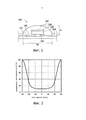
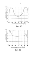
Коэффициент пропускания светового излучения светоотражающей пленки 106 зависит от угла падения светового излучения, падающего из светоизлучающего элемента 105. На фиг. 2 приведена диаграмма, показывающая зависимость коэффициента пропускания светового излучения светоотражающей пленки 106 от угла падения в этом варианте осуществления. Светоотражающая пленка 106 почти не пропускает световое излучение через себя в направлении, перпендикулярном верхней поверхности светоизлучающего элемента 105, но увеличивает количество проходящего светового излучения, если угол падения относительно перпендикулярного направления увеличивается. В частности, если угол падения находится в диапазоне от -30° до 30°, то коэффициент пропускания светового излучения составляет приблизительно 10%. Если угол падения становится меньше -30°, то коэффициент пропускания светового излучения постепенно увеличивается. Кроме того, если угол падения становится меньше -50°, то коэффициент пропускания светового излучения резко увеличивается. Аналогично, если угол падения становится больше 30°, то коэффициент пропускания светового излучения постепенно увеличивается. Кроме того, если угол падения становится больше 50°, то коэффициент пропускания светового излучения резко увеличивается. То есть, коэффициент пропускания светового излучения светоотражающей пленки увеличивается при росте абсолютного значения угла падения светового излучения. Формирование такой отражающей пленки может обеспечить характеристику распределения светового излучения в виде крыльев летучей мыши, как показано на фиг. 4.The light transmittance of the
Используемое здесь выражение "характеристика распределения светового излучения в виде крыльев летучей мыши" означает характеристику распределения светового излучения, имеющую первый пик в первой области с углом распределения светового излучения менее 90°, причем первый пик имеет более высокую интенсивность, чем при угле распределения светового излучения равном 90°, а также второй пик во второй области с углом распределения светового излучения более 90°, причем второй пик имеет более высокую интенсивность, чем при угле распределения светового излучения равном 90°.As used herein, the term “characteristic of the distribution of light radiation in the form of bat wings” means a characteristic of the distribution of light radiation having a first peak in the first region with a light distribution angle of less than 90 °, the first peak having a higher intensity than when the angle of light distribution is 90 °, as well as a second peak in the second region with a light distribution angle of more than 90 °, the second peak having a higher intensity than with a light distribution angle new radiation equal to 90 °.
Светоизлучающий элемент 105 покрыт светопроводящей оболочкой 108. Оболочка 108 расположена на основании, покрывая светоизлучающий элемент 105, чтобы защитить светоизлучающий элемент 105 от внешней среды и оптически контролировать световое излучение, испускаемое светоизлучающим элементом. Оболочка 108 выполнена по существу куполообразной формы. Оболочка 108 покрывает светоизлучающий элемент 105 с расположенной на нем светоотражающей пленкой 106, поверхности токопроводящих дорожек 102, расположенные вокруг светоизлучающего элемента 105, и соединительные участки между светоизлучающим элементом 105, включающие в себя соединительные элементы 103 и токопроводящие дорожки 102. То есть, верхняя поверхность и боковые поверхности светоотражающей пленки 106 контактируют с оболочкой 108, и боковые поверхности светоизлучающего элемента 105, не покрытые светоотражающей пленкой 106, также контактируют с оболочкой 108. Соединительные участки могут быть покрыты прослойкой, а не оболочкой 108. В этом случае оболочку 108 формируют так, чтобы она покрывала верхнюю поверхность прослойки и светоизлучающий элемент. В этом варианте осуществления светоизлучающий элемент 105 непосредственно покрыт оболочкой 108.The light-emitting
Оболочка 108 предпочтительно выполнена так, чтобы она имела круглую или эллипсоидную внешнюю форму на виде сверху, при этом отношение высоты (Н) оболочки в направлении оптической оси к диаметру (ширине W) оболочки на виде сверху составляет менее 0,5. Для оболочки 108, имеющей эллипсоидную форму, имеется главная ось и малая ось, которые можно рассматривать как длину и ширину, но в настоящем описании под диаметром (W) оболочки 108 понимают малую ось. Верхняя поверхность оболочки 108 выполнена в выпуклой изогнутой форме.The
При таком устройстве световое излучение, испускаемое светоизлучающим элементом 105, преломляется на границе между оболочкой 108 и воздухом, благодаря чему можно получить более широкое распределение светового излучения.With such a device, the light radiation emitted by the
Здесь, высота (Н) оболочки означает высоту от установочной поверхности для светоизлучающего элемента 105, как показано на фиг. 1. Ширина (W) оболочки означает ее диаметр, если оболочка имеет круглую нижнюю поверхность, как было упомянуто выше, или, как вариант, означает длину ее наиболее короткой части, если оболочка имеет форму, отличную от круглой.Here, the height (H) of the casing means the height from the mounting surface for the
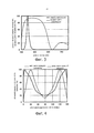
На фиг. 4 показан пример изменения характеристики распределения светового излучения в зависимости от наличия или отсутствия оболочки 108. На фиг. 4 сплошная линия показывает характеристику распределения светового излучения светоизлучающего устройства 100 в первом варианте осуществления. С другой стороны, пунктирная линия показывает характеристику распределения светового излучения светоизлучающего устройства, изготовленного так же как и в первом варианте осуществления за исключением того, что оболочки 108 нет.In FIG. 4 shows an example of a change in the distribution characteristic of light radiation depending on the presence or absence of
Как видно на фиг. 4, для светоизлучающего устройства в первом варианте осуществления первый пик перемещается в направлении, которое уменьшает угол распределения светового излучения, так же как и второй пик перемещается в направлении, которое увеличивает угол распределения светового излучения, по сравнению со светоизлучающим устройством без оболочки 108. Поэтому, светоизлучающее устройство в первом варианте осуществления может дать более широкое распределение светового излучения.As seen in FIG. 4, for the light-emitting device in the first embodiment, the first peak moves in a direction that decreases the angle of distribution of light radiation, just as the second peak moves in a direction that increases the angle of distribution of light radiation, compared with a light-emitting device without a clad 108. Therefore, the light emitting device in the first embodiment can give a wider distribution of light radiation.
При использовании и светоотражающей пленки 106, и оболочки 108 таким способом можно получить требуемую характеристику распределения светового излучения без использования вторичной линзы. То есть, формирование светоотражающей пленки 106 может сократить яркость непосредственно над светоизлучающим элементом 105, в то время как оболочка 108 может сосредоточиться на расширении распределения светового излучения от светоизлучающего элемента 105, что позволяет значительно уменьшить оболочку с функцией линзы.Using both the
Другими словами, обычно уменьшение яркости непосредственно над светоизлучающим элементом при расширении распределения светового излучения возможно только путем регулировки высоты оболочки, в результате чего высота оболочки должна быть увеличена. В отличие от этого, светоизлучающее устройство в этом варианте осуществления включает в себя светоотражающую пленку 106, имеющую пониженную яркость непосредственно над светоизлучающим элементом 105, тем самым достигая характеристики распределения светового излучения в виде крыльев летучей мыши. Таким образом, оболочка 108 может быть выполнена так, чтобы фокусироваться на функции расширения распределения светового излучения. Таким образом, этот вариант осуществления может обеспечить уменьшение размера светоизлучающего устройства.In other words, usually a decrease in brightness directly above the light emitting element when expanding the distribution of light radiation is possible only by adjusting the height of the shell, as a result of which the height of the shell should be increased. In contrast, the light-emitting device in this embodiment includes a
Такое устройство может дать более тонкий модуль задней подсветки (т.е. светоизлучающий модуль), позволяющий сократить неравномерную яркость, как будет сказано ниже. На фиг. 5 в качестве сравнительного примера показана характеристика распределения светового излучения, полученная при использовании вторичной линзы. Даже без использования вторичной линзы светоизлучающее устройство в этом варианте осуществления может дать по существу такую же характеристику распределения светового излучения, что и при использовании вторичной линзы.Such a device can provide a thinner backlight module (i.e., a light emitting module), which allows to reduce uneven brightness, as will be described below. In FIG. 5, as a comparative example, a light distribution characteristic obtained using a secondary lens is shown. Even without the use of a secondary lens, the light emitting device in this embodiment can give substantially the same light emission distribution characteristic as when using the secondary lens.
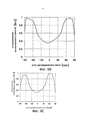
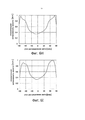
Было изготовлено девять светоизлучающих устройств, имеющих различную высоту (Н) оболочки 108 в направлении оптической оси и различные диаметры (ширину: W) оболочки на виде сверху. Полученные для них характеристики распределения светового излучения показаны на фиг. 6А-6I. Применяемый светоизлучающий элемент представлял собой синий светодиод, имеющий по существу квадратную форму со стороной 600 мкм на виде в плане и толщиной 150 мкм. Светоотражающая пленка 106, сформированная на основной поверхности светоизлучающего элемента 105, выполнена из одиннадцати слоев путем многократного нанесения слоя SiO2 (толщиной 82 нм) и слоя ZrO2 (толщиной 54 нм).Nine light-emitting devices were manufactured having different heights (H) of the
Для каждого из девяти светоизлучающих устройств № 1-9 отношение высоты (Н) оболочки к диаметру (ширине W) оболочки приведено в Таблице 1.For each of the nine light-emitting devices No. 1-9, the ratio of the height (H) of the shell to the diameter (width W) of the shell is shown in Table 1.
Таблица 1Table 1
6AFIG.
6A
6BFIG.
6B
6IFIG.
6I
Как видно из результатов экспериментов, характеристики распределения светового излучения из-за различий диаметра оболочки сильно не меняются. Тем не менее, отношение высоты (Н) оболочки к диаметру (ширине: W) оболочки влияет на свойства распределения светового излучения.As can be seen from the experimental results, the characteristics of the distribution of light radiation due to differences in the diameter of the shell do not change much. However, the ratio of the height (H) of the cladding to the diameter (width: W) of the cladding affects the light distribution properties.
Графики на фиг. 6А-6I показывают, что для того, чтобы получить более широкое распределение светового излучения, отношение (H/W) высоты (Н) к ширине (W) оболочки предпочтительно должно составлять 0,3 или меньше.The graphs in FIG. 6A-6I show that in order to obtain a wider distribution of light radiation, the ratio (H / W) of the height (H) to the width (W) of the cladding should preferably be 0.3 or less.
Ниже будут описаны предпочтительные примеры светоизлучающего устройства 100 в этом варианте осуществления.Preferred examples of the
Основание 101
Основание 101 представляет собой элемент, на котором устанавливают светоизлучающий элемент 105. Основание 101 содержит на своей поверхности токопроводящие дорожки 102, чтобы подавать электроэнергию на светоизлучающий элемент 105.The
Примеры материалов, из которых выполняют основание 101, могут включать в себя керамику и смолы, такие как фенольная смола, эпоксидная смола, полиимидная смола, смола BT, полифталамид (PPA) и полиэтилентерефталат (PET). Среди них смолу предпочтительно выбирают как материал, обладающий низкой стоимостью и способностью к формоизменению. Толщину основания можно выбирать подходящим образом. Основание может представлять собой либо жесткое основание, либо гибкое основание, изготавливаемое с помощью рулонной системы. Жесткое основание может представлять собой тонкое жесткое основание, которое можно сгибать.Examples of materials from which base 101 is made may include ceramics and resins such as phenolic resin, epoxy resin, polyimide resin, BT resin, polyphthalamide (PPA) and polyethylene terephthalate (PET). Among them, the resin is preferably selected as a material having a low cost and shapeability. The thickness of the base can be selected appropriately. The base can be either a rigid base or a flexible base made using a roll system. The rigid base may be a thin rigid base that can be bent.
Чтобы получить светоизлучающее устройство, устойчивое к теплу и световому излучению, в качестве материала основания 101 предпочтительно выбирают керамику. Примеры керамики могут включать в себя оксид алюминия, муллит, форстерит, стеклокерамику, керамику на основе нитрида (напр., AlN) и керамику на основе карбида (напр., SiC). Среди них предпочтительной является керамика, выполненная из алюминия или содержащая алюминий.In order to obtain a light-emitting device resistant to heat and light radiation, ceramics are preferably selected as the
При использовании смолы в качестве материала для основания 101 неорганический наполнитель, такой как стекловолокно, SiO2, TiO2 или Al2O3, смешивают со смолой, тем самым позволяя основанию иметь повышенную механическую прочность и увеличенную оптическую отражательную способность, уменьшенный коэффициент теплового расширения и т.п. Основание 101 может представлять собой любой другой элемент, если оно может отделять и изолировать друг от друга пару токопроводящих дорожек 102. В основании 101 могут использовать так называемое металлическое основание, которое включает в себя металлический элемент с изолирующим слоем, сформированным на нем.When using the resin as the material for the
Токопроводящие дорожки 102
Токопроводящие дорожки 102 представляют собой элементы, электрически соединенные с электродами светоизлучающего элемента 105, и они приспособлены для того, чтобы подавать ток (электроэнергию) извне на светоизлучающий элемент. То есть, токопроводящие дорожки служат в качестве электродов или их части для подачи питания извне. Обычно токопроводящие дорожки выполняют, по меньшей мере, из двух дорожек, а именно, положительной и отрицательной, расположенных на расстоянии друг от друга.The
Каждую токопроводящую дорожку 102 выполняют, по меньшей мере, на верхней поверхности основания, которая служит в качестве установочной поверхности для светоизлучающего элемента 105. Материал для токопроводящих дорожек 102 можно выбирать соответствующим образом в зависимости от материала, использованного для основания 101, способа их изготовления и т.п. Например, если в качестве материала для основания 101 использовали керамику, то токопроводящие дорожки 102 предпочтительно изготавливают из материала, имеющего высокую температуру плавления, которая может выдерживать температуру спекания керамического листа. В частности, в качестве материала для токопроводящих дорожек предпочтительно используют металл, имеющий высокую температуру плавления, такой как вольфрам или молибден. Кроме того, для покрытия вышеупомянутой поверхности токопроводящих дорожек путем нанесения покрытия, напыления, осаждения из паровой фазы и т.д., могут быть взяты другие материалы, такие как никель, золото или серебро.Each
Если в качестве материала основания 101 используют эпоксидный стеклопластик, то в качестве материала для токопроводящих дорожек 102 предпочтительно берут материал, который легко обрабатывается. В случае использования формованной под давлением эпоксидной смолы токопроводящие дорожки 102 выполняют из материала, который может быть легко обработан путем пробивания, травления, изгиба и т.д. и имеет сравнительно высокую механическую прочность. В частности, примеры токопроводящих дорожек могут включать в себя металлы, такие как медь, алюминий, золото, серебро, вольфрам, железо и никель, а также металлический слой или выводную рамку из железоникелевого сплава, фосфористой бронзы, железомедного сплава, молибдена и т.п. Поверхность выводной рамки может быть покрыта металлическим материалом, отличным от металлического материала основного корпуса выводной рамки. Такие металлические материалы могут быть соответственно подобраны, например, только серебро или сплав серебра и меди, золото, алюминий или родий. В качестве альтернативы, токопроводящие дорожки могут быть выполнены из нескольких слоев с использованием серебра или каждого сплава. Подходящие способы покрытия металлическим материалом могут включать в себя распыление, осаждение из паровой фазы и т.п., а также нанесение покрытия.If epoxy fiberglass is used as the
Соединительный элемент 103The connecting
Соединительные элементы 103 представляют собой элементы, предназначенные для фиксации светоизлучающего элемента 105 на основании 101 или проводящих дорожках 102. При установке методом перевернутого кристалла проводящие элементы используют в качестве соединительных элементов так же, как и в этом варианте осуществления. В частности, подходящие материалы для соединительных элементов могут включать в себя золотосодержащий сплав, содержащий серебро сплав, содержащий палладий сплав, содержащий индий сплав, свинцово-палладиевый сплав, золото-галлиевый сплав, золото-оловянный сплав, оловянный сплав, олово-медный сплав, олово-медно-серебряный сплав, золото-германиевый сплав, золото-кремниевый сплав, содержащий алюминий сплав, медно-индиевый сплав, и смесь металла и флюса,The connecting
Подходящие формы соединительного элемента 103 могут включать в себя следующие: жидкостного типа, пастообразного типа и/или твердого типа (напр., в виде листа, в виде блока, в виде провода и/или в виде порошка). Форма соединительного элемента может быть подходящим образом выбрана, исходя из его состава, формы основания и т.п. Эти соединительные элементы 103 могут быть выполнены из одного элемента или из сочетания нескольких видов элементов.Suitable forms of the connecting
Изолирующий элемент 104Insulating
Токопроводящие дорожки 102 предпочтительно покрывают изолирующим элементом 104, за исключением частей, электрически соединенных со светоизлучающим элементом 105 и другими материалами. То есть, как показано на соответствующих фигурах, сопротивление для изоляции и покрытия токопроводящих дорожек 102 может быть нанесено на основание. Изолирующий элемент 104 может функционировать в качестве такого сопротивления.The
В случае нанесения изолирующего элемента 104 в изолирующем элементе может содержаться белый наполнитель. Белый наполнитель, содержащийся в изолирующем элементе, может сократить утечку и поглощение светового излучения, тем самым, позволяя увеличить эффективность светового излучения светоизлучающего устройства 100, а также изолировать токопроводящие дорожки 102.In the case of applying the insulating
Материал для изолирующего элемента 104 можно соответствующим образом выбрать, исходя из того, чтобы этот материал не поглощал световое излучение от светоизлучающего элемента и обладал изолирующими свойствами. Примеры материала для изолирующего элемента могут включать в себя эпоксидную, силиконовую, модифицированную силиконовую, уретановую, оксетановую, акриловую, поликарбонатную и полиимидную смолу.The material for the insulating
Светоизлучающий элемент 105
Светоизлучающий элемент 105, установленный на основании, может быть известен в области техники. В этом варианте осуществления в качестве светоизлучающего элемента 105 предпочтительно используют светодиод.A
Можно выбрать светоизлучающий элемент 105, который излучает световое излучение соответствующей длины волны. Например, в синем или зеленом светоизлучающем элементе может быть использован ZnSe, нитридный полупроводник (InxAlyGa1-x-yN, 0 ![]()
![]()
![]()
![]()
![]()
![]()
Можно выбрать различные длины излучаемых волн в зависимости от материала полупроводникового слоя и его соотношения смешанных кристаллов. Светоизлучающий элемент может содержать положительный и отрицательный электроды на одной и той же поверхности, чтобы можно было выполнить установку методом перевернутого кристалла, либо, в качестве альтернативы, он может иметь положительный и отрицательный электроды на разных своих поверхностях.You can choose different lengths of the emitted waves depending on the material of the semiconductor layer and its ratio of mixed crystals. The light emitting element may contain positive and negative electrodes on the same surface so that it can be installed by the inverted crystal method, or, alternatively, it may have positive and negative electrodes on its different surfaces.
Светоизлучающий элемент 105 в этом варианте осуществления содержит светопроводящую подложку, и на подложке выполнен полупроводниковый слой. Полупроводниковый слой включает в себя слой полупроводника n-типа, активный слой и слой полупроводника p-типа, выполненные в таком порядке. Электрод n-типа выполняют на слое полупроводника n-типа, а электрод p-типа выполняют на слое полупроводника p-типа.The
Как показано на фиг. 1, светоизлучающий элемент 105 установлен методом перевернутого кристалла на токопроводящие дорожки 102, расположенные на поверхности основания 101, посредством соединительных элементов 103. Поверхность светоизлучающего элемента 105, противоположная его поверхности, на которой выполнены электроды, то есть, основная поверхность светопроводящей подложки, будет служить в качестве светоизлучающей поверхности. Тем не менее, в том варианте изобретения светоотражающая пленка 106 выполнена на светоизлучающей поверхности, и, таким образом, боковая поверхность светоизлучающего элемента 105 практически служит в качестве светоизлучающей поверхности. То есть, часть светового излучения, излучаемого светоизлучающим элементом 105 и направляемая в сторону основной поверхности светоизлучающего элемента 105, возвращается на светоизлучающий элемент 105 с помощью светоотражающей пленки 106, затем снова отражается внутри светоизлучающего элемента 105 и, наконец, выходит через боковые поверхности светоизлучающего элемента 105. Поэтому, свойства распределения светового излучения светоизлучающего устройства 100 (см. пунктирную линию на фиг. 4) демонстрируют свойства сочетания светового излучения, проходящего через светоотражающую пленку 106, и светового излучения, излучаемого из боковых поверхностей светоизлучающего элемента 105.As shown in FIG. 1, the
Светоизлучающий элемент 105 расположен так, чтобы охватывать область между двумя токопроводящими дорожками 102, которые изолированы и разделены на положительную и отрицательную стороны. Светоизлучающий элемент 105 электрически соединен и механически закреплен на токопроводящих дорожках с помощью проводящих соединительных элементов 103. Чтобы установить светоизлучающий элемент 105, можно применять способ, использующий подпрессовку, а также способ, использующий паяльную пасту. В качестве светоизлучающего элемента 105 также можно использовать малогабаритное изделие, которое включает в себя светоизлучающий элемент, заключенный в смолу или подобное. Форму и структуру светоизлучающего элемента 105 можно выбрать соответствующим образом.The
Как будет описано ниже, в случае светоизлучающего устройства, включающего в себя элемент преобразования длины волны, в светоизлучающем элементе соответствующим образом применяют нитридный полупроводник (InxAlyGa1-x-yN, 0 ![]()
![]()
![]()
![]()
![]()
![]()
Хотя в качестве примера был описан вариант, в котором применяют установку методом перевернутого кристалла, в некоторых вариантах осуществления настоящего изобретения могут использовать установку, в которой изоляция стороны основания светоизлучающего элемента служит в качестве установочной поверхности, а электроды, сформированные на верхней поверхности светоизлучающего элемента, соединены с дорожками. В этом случае верхняя поверхность светоизлучающего элемента представляет собой сторону с электродами, и на стороне с электродами расположена светоотражающая пленка.Although an example has been described in which an inverted crystal installation is used, in some embodiments of the present invention, an installation can be used in which the base side insulation of the light emitting element serves as a mounting surface and the electrodes formed on the upper surface of the light emitting element are connected with the tracks. In this case, the upper surface of the light emitting element is a side with electrodes, and a reflective film is arranged on the side with electrodes.
Светоотражающая пленка 106
Светоотражающая пленка 106 выполнена на стороне светоизлучающей поверхности, которая представляет собой основную поверхность светоизлучающего элемента 105.The
Материал для светоотражающей пленки может представлять собой материал, который отражает, по меньшей мере, световое излучение, излучаемое светоизлучающим элементом 105, например, металл или смолу, содержащую белый наполнитель.The material for the retroreflective film may be a material that reflects at least the light radiation emitted by the
Для изготовления отражающей пленки, обладающей меньшей способностью поглощать световое излучение, можно использовать диэлектрическую многослойную пленку. Кроме того, коэффициент отражения светоотражающей пленки можно соответствующим образом отрегулировать путем проектирования диэлектрической многослойной пленки, либо ее коэффициент отражения также можно контролировать путем регулировки угла светового излучения. В частности, коэффициент отражения увеличивается в направлении, перпендикулярном светоизлучающей поверхности (также называемом направлением оптической оси), и уменьшается при большом угле относительно оптической оси вследствие увеличения коэффициента пропускания светового излучения отражающей пленки, что может дать распределение светового излучения в виде крыльев летучей мыши.For the manufacture of a reflective film having a lower ability to absorb light radiation, a dielectric multilayer film can be used. In addition, the reflection coefficient of the reflective film can be adjusted accordingly by designing the dielectric multilayer film, or its reflection coefficient can also be controlled by adjusting the angle of light emission. In particular, the reflection coefficient increases in the direction perpendicular to the light emitting surface (also called the direction of the optical axis) and decreases at a large angle relative to the optical axis due to an increase in the transmittance of the light radiation of the reflective film, which can give the distribution of light radiation in the form of bat wings.
Касательно диапазона длин отраженных волн в направлении оптической оси диэлектрической многослойной пленки, т.е. в направлении, перпендикулярном верхней поверхности светоизлучающего элемента, как показано на фиг. 3, предпочтительно расширить область на стороне больших длин волн диапазона длин отраженных волн относительно пиковой длины волны излучения светоизлучающего элемента 105.Regarding the length range of the reflected waves in the direction of the optical axis of the dielectric multilayer film, i.e. in a direction perpendicular to the upper surface of the light emitting element, as shown in FIG. 3, it is preferable to expand the region on the long wavelength side of the reflected wavelength range with respect to the peak radiation wavelength of the
Причина этого заключается в изменении угла от оптической оси, другими словами, когда угол от оптической оси падающего светового излучения увеличивается, то диапазон длин отраженных волн диэлектрической многослойной пленки сдвигается в сторону коротких длин волн. Путем расширения диапазона длин отраженных волн в сторону больших длин волн относительно длины излучаемой волны можно поддерживать адекватный коэффициент отражения вплоть до широкого угла, то есть, когда световое излучение падает от светоизлучающего элемента под большим углом относительно оптической оси.The reason for this is a change in the angle from the optical axis, in other words, when the angle from the optical axis of the incident light increases, the range of reflected wavelengths of the dielectric multilayer film is shifted toward short wavelengths. By expanding the range of reflected wavelengths towards longer wavelengths relative to the emitted wavelength, it is possible to maintain an adequate reflection coefficient up to a wide angle, that is, when light radiation is incident from the light emitting element at a large angle relative to the optical axis.
Материалы, пригодные для использования в диэлектрической многослойной пленке, могут представлять собой пленку оксида металла, пленку нидрида металла, оксинитридную пленку и т.п. Также можно использовать органические материалы, такие как силиконовая смола или фторопластовая смола. Тем не менее, материал для диэлектрической многослойной пленки можно выбрать из материалов, отличных от описанных выше.Materials suitable for use in a dielectric multilayer film may be a metal oxide film, a metal nitride film, an oxynitride film, and the like. Organic materials such as silicone resin or fluoroplastic resin can also be used. However, the material for the dielectric multilayer film can be selected from materials other than those described above.
Оболочка 108
Материалы, пригодные для использования в качестве оболочки 108, могут представлять собой светопроводящие материалы, включающие в себя эпоксидную смолу, силиконовую смолу, их смесь или стекло. Среди них предпочтительно выбирают силиконовую смолу, учитывая устойчивость к световому излучению и способность к формоизменению.Materials suitable for use as
Оболочка 108 может содержать: светорассеивающий материал, материал, преобразующий длину волны, такой как люминофор или квантовые примеси, которые поглощают часть светового излучения от светоизлучающего элемента 105, чтобы испускать световое излучение, длина волны которого отличается от длины волны светового излучения, излучаемого светоизлучающим элементом; и пигмент, соответствующий цвету излучаемого светоизлучающим элементом светового излучения.
В случае добавления этих материалов в оболочку 108 предпочтительно использовать те, которые не будут негативно влиять на свойства распределения светового излучения. Например, материал, имеющий размер частиц 0,2 мкм или менее, является предпочтительным, так как менее вероятно, что он окажет негативное влияние на свойства распределения светового излучения. Используемое в данной спецификации выражение "размер частиц" означает средний размер частиц, а средний размер частиц измеряют с помощью прибора Фишера (Fisher-SubSieve-Sizers (F.S.S.S.No)) с использованием метода воздухопроницаемости.If these materials are added to the
Оболочка 108 может быть выполнена посредством компрессионного формования или инжекционного формования, чтобы закрыть светоизлучающий элемент 105. Как вариант, материал для оболочки 108 имеет оптимальную вязкость, чтобы его можно было нанести в виде капли или наложить на светоизлучающий элемент 105, тем самым, контролируя форму оболочки 108 посредством поверхностного натяжения самого материала.The
При последнем способе образования не требуется форма, так что оболочку можно выполнить более простым способом. Помимо регулирования вязкости основного материала оболочки 108 вязкость материала оболочки можно регулировать, используя вышеупомянутый светорассеивающий материал, материал, преобразующий длину волны, и/или пигмент, для формирования оболочки 108 с требуемым уровнем вязкости.In the latter method of formation, a mold is not required, so that the shell can be made in a simpler way. In addition to adjusting the viscosity of the base material of the
Второй вариантSecond option
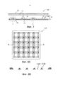
На фиг.7 приведен вид в поперечном сечении светоизлучающего модуля 300, включающего в себя светоизлучающее устройство 200 во втором варианте осуществления. В этом варианте осуществления на основании 101 установлено несколько светоизлучающих элементов 105 через заданные интервалы. По меньшей мере, один светоотражающий элемент 110 расположен между соседними светоизлучающими элементами 105, чтобы отражать световое излучение, испускаемое под небольшим углом относительно верхней поверхности светоизлучающего элемента (т.е. верхней поверхности основания 101). То есть светоизлучающее устройство 200 представляет собой интегрированное светоизлучающее устройство, которое включает в себя несколько светоизлучающих устройств 100 первого варианта осуществления и светоотражающий элемент 110, расположенный между соответствующими светоизлучающими устройствами 100. Светорассеивающая пластина 111, предназначенная для рассеивания светового излучения от светоизлучающего элемента 105, расположена над светоизлучающими устройствами 100 и светоотражающим элементом 110 и по существу параллельна верхним поверхностям светоизлучающих элементов. Слой 112 преобразования длины волны, предназначенный для преобразования части светового излучения, испускаемого светоизлучающими элементами 105, в световое излучение, имеющее другую длину волны, расположен над светорассеивающей пластиной 111 и по существу параллелен светорассеивающей пластине 111.7 is a cross-sectional view of a
В общем, поскольку отношение расстояния между основанием 101 и светорассеивающей пластиной 111 (в дальнейшем называемого оптическим расстоянием: OD) к расстоянию между соседними светоизлучающими элементами (в дальнейшем называемому шагом) уменьшается, то количество светового излучения между светоизлучающими элементами 105 на поверхности светорассеивающей пластины 111 становится малым, вызывая темное пространство.In general, since the ratio of the distance between the base 101 and the light diffusing plate 111 (hereinafter referred to as the optical distance: OD) to the distance between adjacent light emitting elements (hereinafter referred to as the pitch) decreases, the amount of light radiation between the
Однако когда устройство содержит светоотражающий элемент 110, расположенный таким образом, световое излучение, отражаемое светоотражающим элементом 110, компенсирует количество светового излучения между светоизлучающими элементами, в результате чего можно снизить неравномерность яркости на поверхности светорассеивающей пластины 111 даже в области с меньшим отношением OD/шаг.However, when the device comprises a
В частности, в светоизлучающем устройстве 200 по второму варианту осуществления изобретения угол θ наклона светоотражающей поверхности светоотражающего элемента 110 относительно основания 101 задан так, что неравномерность яркости на поверхности светорассеивающей пластины 111 уменьшается с учетом свойств распределения светового излучения соответствующих светоизлучающих устройств 100. Что касается свойств распределения светового излучения нескольких светоизлучающих устройств 100, каждое светоизлучающее устройство 100 предпочтительно имеет такие характеристики распределения светового излучения, что количество светового излучения становится большим в области с большим углом распределения светового излучения, т.е. в области при угле распределения светового излучения около ± 90°, чтобы снизить неравномерность яркости на поверхности светорассеивающей пластины 111 и получить тонкое светоизлучающее устройство 200.In particular, in the
Если отношение OD/шаг небольшое, например, 0,2 или менее, то угол наклона, под которым падающее световое излучение входит в светоотражающий элемент 110, меньше, чем 22° относительно светоизлучающей поверхности светоизлучающего элемента 105. Таким образом, чтобы увеличить коэффициент отражения светового излучения светоотражающим элементом 110 при низком отношении OD/шаг, равном 0,2 или меньше, характеристика распределения светового излучения светоизлучающего устройства 100 предпочтительно такова, что, например, количество светового излучения под углом наклона менее 20° относительно верхней поверхности основания является большим. В частности, первый и второй пики интенсивности излучения предпочтительно расположены в диапазоне угла наклона менее 20°. Здесь угол наклона, равный 20°, соответствует углам распределения светового излучения 20° и 160° на фиг. 4. Другими словами, первый пик интенсивности излучения расположен в диапазоне углов распределения светового излучения менее 20°, а второй пик интенсивности излучения расположен в диапазоне углов распределения светового излучения большее 160°, как показано на фиг. 4. Количество светового излучения в диапазоне углов наклона менее 20° предпочтительно составляет 30% или больше от общего количества светового излучения, и более предпочтительно - 40% или более.If the OD / step ratio is small, for example 0.2 or less, then the angle of inclination at which the incident light enters the
Светоотражающий элемент 110
Светоотражающий элемент 110 расположен между соседними светоизлучающими элементами 105.A
Светоотражающий элемент может быть выполнен из материала, который отражает, по меньшей мере, световое излучение, имеющее длину волны излучения светоизлучающего элемента 105. Например, для светоотражающего элемента можно использовать металлическую пластину или смолу, содержащую белый наполнитель.The reflective element may be made of a material that reflects at least light radiation having a radiation wavelength of the
Для изготовления отражающей поверхности, обладающей меньшей способностью поглощать световое излучение, можно использовать диэлектрическую многослойную пленку в качестве отражающей поверхности с меньшим поглощением светового излучения. Кроме того, коэффициент отражения светоотражающего элемента можно соответствующим образом отрегулировать путем проектирования диэлектрической многослойной пленки, либо ее коэффициент отражения также можно контролировать посредством угла светового излучения.For the manufacture of a reflective surface having a lower ability to absorb light radiation, a dielectric multilayer film can be used as a reflective surface with less absorption of light radiation. In addition, the reflection coefficient of the reflective element can be adjusted accordingly by designing a dielectric multilayer film, or its reflection coefficient can also be controlled by the angle of light emission.
Высота светоотражающего элемента 110 и угол θ наклона светоотражающей поверхности относительно поверхности основания 101 можно задать равным соответствующему значению. Отражающая поверхность светоотражающего элемента 110 может быть плоской поверхностью или изогнутой поверхностью. Чтобы получить требуемые свойства распределения светового излучения, можно задать подходящий угол θ наклона и форму отражающей поверхности. Высоту светоотражающего элемента 110 предпочтительно задают равной 0,3 или менее, более предпочтительно 0,2 или менее, от расстояния между соседними светоизлучающими элементами. Такое расположение может дать тонкий светоизлучающий модуль 300 с меньшей неравномерностью яркости.The height of the
Для светоизлучающего устройства 200, используемого в среде, где температура использования имеет тенденцию к существенному изменению, коэффициент линейного расширения светоотражающего элемента 110 должен быть близким к соответствующему коэффициенту основания 101. В случае, когда коэффициент линейного расширения светоотражающего элемента 110 значительно отличается от соответствующего коэффициента основания 101, может произойти коробление в светоизлучающем устройстве 200 из-за изменения температуры или, иначе, взаимное расположение компонентов, в частности, светоизлучающего устройства 100 и светоотражающего элемента 110 может сместиться, тем самым, возможно, не позволяя получить желаемые оптические свойства. Однако коэффициент линейного расширения является физическим свойством и, следовательно, в действительности имеется не так много альтернатив. По этой причине светоотражающий элемент 110 предпочтительно выполняют из пленочного формованного компонента, который является упруго деформируемым, чтобы сократить возможность возникновения коробления светоизлучающего устройства 200 даже в том случае, когда коэффициент линейного расширения светоотражающего элемента значительно отличается от соответствующего коэффициента основания. Это связано с тем, что светоотражающий элемент 110, выполненный из менее упруго деформируемого материала, например, из твердого материала, имеет тенденцию расширяться при сохранении своей формы, но светоотражающий элемент в форме пленки может соответствующим образом деформироваться, чтобы компенсировать его расширение.For the light-emitting
Предпочтительно несколько светоотражающих элементов 110 соединены вместе на плоскости так, чтобы имелись сквозные отверстия 113, где располагают светоизлучающие устройства 200. На фиг. 8 показана такая плоская светоотражающая пластина 110'. На фиг. 8А приведен вид сверху светоотражающей пластины 110', а на фиг. 8В показан вид в разрезе, взятом вдоль прямой А-А, показанной на фиг. 8А. Такая светоотражающая пластина 110' может быть выполнена путем литья металла, вакуумного формования, прессования и т.п. Светоотражающая пластина 110' расположена на основании 101. Светоотражающий элемент 110 может быть выполнен способом, который включает в себя нанесение светоотражающей смолы непосредственно на основание 101 и т.п. Высоту светоотражающего элемента 110 предпочтительно задают равной 0,3 или менее от расстояния между соседними светоизлучающими элементами, и, например, более предпочтительно 0,2 или менее, от расстояния между соседними светоизлучающими элементами.Preferably, several
Пример 1Example 1
В этом примере, как показано на фиг. 1, для основания 101 использовали эпоксидный стеклопластик, а в качестве токопроводящих дорожек использовали медный материал толщиной 35 мкм.In this example, as shown in FIG. 1, epoxy fiberglass was used for
В качестве светоизлучающего элемента 105 можно использовать нитридный синий светодиод. Светодиод имеет приблизительно квадратную форму со стороной 600 мкм на виде в плане и толщиной 150 мкм. В качестве изолирующего элемента 104 можно использовать эпоксидный белый паяльный резист.As the
Светоотражающая пленка 106, сформированная на основной поверхности светоизлучающего элемента 105, выполнена из одиннадцати слоев путем многократного нанесения слоя SiO2 (толщиной 82 нм) и слоя ZrO2 (толщиной 54 нм).A
На данный момент коэффициент пропускания светового излучения отражающей пленки 106 показан на фиг. 2. Коэффициент пропускания светового излучения в направлении, перпендикулярном основной поверхности светоизлучающего элемента (т.е. в направлении оптической оси) является низким, и коэффициент пропускания светового излучения отражающей пленки увеличивается по мере увеличения угла отклонения от оптической оси.Currently, the transmittance of light radiation of the
Светоизлучающий элемент 105 покрыт оболочкой 108. Оболочка 108 выполнена из силиконовой смолы и имеет высоту (Н) 1,0 мм и диаметр нижней поверхности (W) 3,0 мм.The
При таком устройстве световое излучение, испускаемое светоизлучающим элементом 105, преломляется на границе между оболочкой 108 и воздухом, что расширяет диапазон углов распределения светового излучения. Характеристика распределения светового излучения светоизлучающего устройства 100, полученного таким образом, показана сплошной линией на фиг. 4. Характеристика распределения светового излучения, полученная для светоизлучающего устройства без оболочки 108, показана пунктирной линией на фиг. 4. Таким образом, оболочку 108 используют вместе со светоотражающей пленкой 106, благодаря чему можно достичь более низкого отношения OD/шаг.With such a device, the light radiation emitted by the
Пример 2Example 2
В примере 2 несколько светоизлучающих элементов 105 из примера 1 установлено на основании 101, и, по меньшей мере, один светоотражающий элемент 110 расположен между соседними светоизлучающими элементами. В данном случае шаг составляет 12,5 мм.In Example 2, several light-emitting
Светоотражающий элемент 110 имеет плоскую форму в виде светоотражающей пластины, которая выполнена с использованием полипропиленового листа, содержащего наполнитель TiO2 (толщиной (t) 02 мм), посредством вакуумного формования, чтобы получить угол θ отражения (т.е. угол наклона) 55° и высоту 2,4 мм. Светоотражающий элемент 110 представляет собой плоскую светоотражающую пластину, показанную на фиг. 8 и расположенную на изолирующем элементе 104.The
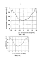
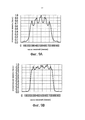
Над светоотражающим элементом 110 расположена молочно-белая светорассеивающая пластина 111 и слой 112 преобразования длины волны, чтобы получить жидкокристаллическую подсветку (т.е. светоизлучающий модуль). При таком устройстве на фиг. 9А и 9В показан результат сравнения неравномерности яркости на поверхности светорассеивающей пластины 111 для случая наличия и отсутствия светоотражающего элемента 110. На фиг. 9А показан светоизлучающий модуль без светоотражающего элемента, а на фиг. 9В показан светоизлучающий модуль, содержащий светоотражающий элемент. Как показано на фиг. 9А и 9В, в случае, когда светоотражающий элемент отсутствует, относительная яркость уменьшается до диапазона примерно от 0,6 до 0,7 в области, где относительная яркость имеет тенденцию быть высокой (т.е. в диапазоне числа пикселей от примерно 250 до примерно 720). С другой стороны, в случае, когда имеется светоотражающий элемент, относительная яркость не снижается ниже 0,7 в области, где относительная яркость имеет тенденцию быть высокой (т.е. в диапазоне числа пикселей от примерно 250 до примерно 720). Другими словами, видно, что при наличии светоотражающего элемента сокращается неравномерность яркости.A milk-white light-diffusing
Светоизлучающее устройство и светоизлучающий модуль в соответствии с настоящими вариантами осуществления можно применять в качестве подсветки для жидкокристаллических дисплеев, различных осветительных приборах и т.п.The light emitting device and the light emitting module according to the present embodiments can be used as a backlight for liquid crystal displays, various lighting devices, and the like.
Claims (33)
Applications Claiming Priority (5)
| Application Number | Priority Date | Filing Date | Title |
|---|---|---|---|
| JP2015200445 | 2015-10-08 | ||
| JP2015-200445 | 2015-10-08 | ||
| JP2016197968A JP6506899B2 (en) | 2015-10-08 | 2016-10-06 | Light emitting device, integrated light emitting device and light emitting module |
| JP2016-197968 | 2016-10-06 | ||
| PCT/JP2016/004528 WO2017061127A1 (en) | 2015-10-08 | 2016-10-07 | Light-emitting device, integrated light-emitting device, and light-emitting module |
Publications (3)
| Publication Number | Publication Date |
|---|---|
| RU2018112372A RU2018112372A (en) | 2019-10-07 |
| RU2018112372A3 RU2018112372A3 (en) | 2019-12-05 |
| RU2717381C2 true RU2717381C2 (en) | 2020-03-23 |
Family
ID=58538425
Family Applications (1)
| Application Number | Title | Priority Date | Filing Date |
|---|---|---|---|
| RU2018112372A RU2717381C2 (en) | 2015-10-08 | 2016-10-07 | Light-emitting device, integrated light-emitting device and light-emitting module |
Country Status (8)
| Country | Link |
|---|---|
| JP (3) | JP6506899B2 (en) |
| KR (1) | KR102632427B1 (en) |
| CN (2) | CN113437202A (en) |
| AU (1) | AU2016238924B2 (en) |
| BR (1) | BR112018006931B1 (en) |
| CA (1) | CA2999401A1 (en) |
| RU (1) | RU2717381C2 (en) |
| TW (2) | TWI799754B (en) |
Families Citing this family (15)
| Publication number | Priority date | Publication date | Assignee | Title |
|---|---|---|---|---|
| JP7082273B2 (en) * | 2017-07-21 | 2022-06-08 | 日亜化学工業株式会社 | Light emitting device, integrated light emitting device and light emitting module |
| CN116884966A (en) | 2017-07-21 | 2023-10-13 | 日亚化学工业株式会社 | Backlight device and light source |
| CN109390327B (en) * | 2017-08-02 | 2020-10-30 | 吴裕朝 | Light-emitting device, backlight module applying same, light source module and preparation method thereof |
| JP2019046789A (en) * | 2017-08-31 | 2019-03-22 | 日亜化学工業株式会社 | Light-emitting device |
| KR102631105B1 (en) * | 2017-08-31 | 2024-01-30 | 니치아 카가쿠 고교 가부시키가이샤 | Light emitting device |
| JP7082272B2 (en) * | 2017-09-27 | 2022-06-08 | 日亜化学工業株式会社 | Light emitting device |
| JP7174216B2 (en) * | 2017-10-23 | 2022-11-17 | 日亜化学工業株式会社 | Light-emitting modules and integrated light-emitting modules |
| TWI793203B (en) * | 2017-10-26 | 2023-02-21 | 晶元光電股份有限公司 | Light-emitting device |
| JP6870592B2 (en) | 2017-11-24 | 2021-05-12 | 豊田合成株式会社 | Light emitting device |
| JP7177331B2 (en) | 2018-06-29 | 2022-11-24 | 日亜化学工業株式会社 | light emitting device |
| JP7180552B2 (en) * | 2019-06-21 | 2022-11-30 | 豊田合成株式会社 | Manufacturing control method for light emitting device |
| JP7226131B2 (en) | 2019-06-25 | 2023-02-21 | 豊田合成株式会社 | Light emitting device and manufacturing method thereof |
| CN112485803A (en) * | 2019-08-21 | 2021-03-12 | Oppo广东移动通信有限公司 | Laser emitting device, manufacturing method thereof and flight time measuring device |
| WO2022085668A1 (en) * | 2020-10-20 | 2022-04-28 | 大日本印刷株式会社 | Surface-emitting device, display device, sealing member sheet for surface-emitting device, and method for manufacturing surface-emitting device |
| CN116779744A (en) * | 2023-06-30 | 2023-09-19 | 淮安澳洋顺昌光电技术有限公司 | Chip-level LED packaging element |
Citations (7)
| Publication number | Priority date | Publication date | Assignee | Title |
|---|---|---|---|---|
| JP2002280614A (en) * | 2001-03-14 | 2002-09-27 | Citizen Electronics Co Ltd | Light emitting diode |
| RU2001119633A (en) * | 2001-07-17 | 2003-07-10 | Ооо Нпц Оэп "Оптэл" | LIGHT-EMITTING DIODE |
| JP2006049857A (en) * | 2004-06-29 | 2006-02-16 | Fuji Photo Film Co Ltd | Light source, light source manufacturing method and color thermal printer |
| RU53500U1 (en) * | 2005-11-22 | 2006-05-10 | Емельян Михайлович Гамарц | ELECTROLUMINESCENT RADIATOR |
| JP2011138849A (en) * | 2009-12-28 | 2011-07-14 | Nichia Corp | Light emitting device and method of manufacturing the same |
| RU2012110241A (en) * | 2011-03-23 | 2013-09-27 | Сони Корпорейшн | LIGHT SCHEME BLOCK, LIGHTING DEVICE AND DISPLAY |
| RU151161U1 (en) * | 2014-08-19 | 2015-03-20 | Общество с ограниченной ответственностью "ЭНЕРКОМ" | A WHITE LIGHT SOURCE AND A LAMP CONTAINING SUCH A SOURCE |
Family Cites Families (29)
| Publication number | Priority date | Publication date | Assignee | Title |
|---|---|---|---|---|
| US6155699A (en) * | 1999-03-15 | 2000-12-05 | Agilent Technologies, Inc. | Efficient phosphor-conversion led structure |
| JP2001257381A (en) * | 2000-03-13 | 2001-09-21 | Sharp Corp | Light-emitting diode, manufacturing method therefor and illumination device |
| US6345903B1 (en) * | 2000-09-01 | 2002-02-12 | Citizen Electronics Co., Ltd. | Surface-mount type emitting diode and method of manufacturing same |
| AU2002217845A1 (en) * | 2000-11-16 | 2002-05-27 | Emcore Corporation | Microelectronic package having improved light extraction |
| RU2207663C2 (en) * | 2001-07-17 | 2003-06-27 | Ооо Нпц Оэп "Оптэл" | Light-emitting diode |
| JP2004253436A (en) * | 2003-02-18 | 2004-09-09 | Citizen Electronics Co Ltd | Light emitting diode |
| DE102004001312B4 (en) * | 2003-07-25 | 2010-09-30 | Seoul Semiconductor Co., Ltd. | Chip light-emitting diode and method for its production |
| JP2006261540A (en) * | 2005-03-18 | 2006-09-28 | Stanley Electric Co Ltd | Light emitting device |
| US7375379B2 (en) * | 2005-12-19 | 2008-05-20 | Philips Limileds Lighting Company, Llc | Light-emitting device |
| KR100649765B1 (en) * | 2005-12-21 | 2006-11-27 | 삼성전기주식회사 | Led package and back light unit using the same |
| US7626210B2 (en) * | 2006-06-09 | 2009-12-01 | Philips Lumileds Lighting Company, Llc | Low profile side emitting LED |
| JP2008041290A (en) * | 2006-08-02 | 2008-02-21 | Akita Denshi Systems:Kk | Lighting device and manufacturing method therefor |
| US8755005B2 (en) * | 2008-09-24 | 2014-06-17 | Koninklijke Philips N.V. | Thin edge backlight with LEDS optically coupled to the back surface |
| JP2010092672A (en) * | 2008-10-06 | 2010-04-22 | Harison Toshiba Lighting Corp | Backlight device, and display device |
| KR101867106B1 (en) * | 2010-03-30 | 2018-06-12 | 다이니폰 인사츠 가부시키가이샤 | Resin-attached leadframe for led, semiconductor device, method for manufacturing semiconductor device and method for manufacturing resin-attached leadframe for led |
| US9341766B2 (en) * | 2010-06-15 | 2016-05-17 | Sharp Kabushiki Kaisha | Lighting device, display device and television device |
| JP5178796B2 (en) * | 2010-09-10 | 2013-04-10 | 三菱電機株式会社 | Light emitting device and lighting device |
| JP5401534B2 (en) * | 2011-03-25 | 2014-01-29 | シャープ株式会社 | LIGHT EMITTING DEVICE, LIGHTING DEVICE, AND DISPLAY DEVICE |
| JP5796209B2 (en) * | 2011-05-23 | 2015-10-21 | パナソニックIpマネジメント株式会社 | LIGHT EMITTING DEVICE AND LIGHTING DEVICE USING THE SAME |
| US8624482B2 (en) * | 2011-09-01 | 2014-01-07 | Toshiba Techno Center Inc. | Distributed bragg reflector for reflecting light of multiple wavelengths from an LED |
| JP2013077798A (en) * | 2011-09-14 | 2013-04-25 | Toyoda Gosei Co Ltd | Glass sealing led lamp and manufacturing method of the same |
| TW201413347A (en) * | 2012-09-19 | 2014-04-01 | Chi Lin Technology Co Ltd | Backlight module having light wave length converting element |
| TWI528083B (en) * | 2012-11-29 | 2016-04-01 | 鴻海精密工業股份有限公司 | Backlight module |
| JP2014187095A (en) * | 2013-03-22 | 2014-10-02 | Toshiba Lighting & Technology Corp | Led module and illumination device |
| JP6179854B2 (en) * | 2013-07-23 | 2017-08-16 | パナソニックIpマネジメント株式会社 | lighting equipment |
| JP6273124B2 (en) * | 2013-11-08 | 2018-01-31 | シチズン電子株式会社 | LED lighting device |
| US9890911B2 (en) * | 2013-12-19 | 2018-02-13 | Koninklijke Philips N.V. | LED module with uniform phosphor illumination |
| CN104766916A (en) * | 2014-01-07 | 2015-07-08 | 易美芯光(北京)科技有限公司 | LED integrated light source adopting inverted blue light chip for packaging |
| CN103872223A (en) * | 2014-01-26 | 2014-06-18 | 上海瑞丰光电子有限公司 | LED (light-emitting diode) chip scale packaging method |
-
2016
- 2016-10-06 JP JP2016197968A patent/JP6506899B2/en active Active
- 2016-10-07 AU AU2016238924A patent/AU2016238924B2/en active Active
- 2016-10-07 CA CA2999401A patent/CA2999401A1/en active Pending
- 2016-10-07 TW TW109137811A patent/TWI799754B/en active
- 2016-10-07 RU RU2018112372A patent/RU2717381C2/en active
- 2016-10-07 KR KR1020160129813A patent/KR102632427B1/en active IP Right Grant
- 2016-10-07 BR BR112018006931-0A patent/BR112018006931B1/en active IP Right Grant
- 2016-10-07 TW TW105132674A patent/TWI712181B/en active
- 2016-10-08 CN CN202110686880.2A patent/CN113437202A/en active Pending
- 2016-10-08 CN CN201611144127.6A patent/CN106571421B/en active Active
-
2018
- 2018-04-17 JP JP2018079375A patent/JP7175099B2/en active Active
-
2021
- 2021-08-06 JP JP2021129946A patent/JP7252483B2/en active Active
Patent Citations (7)
| Publication number | Priority date | Publication date | Assignee | Title |
|---|---|---|---|---|
| JP2002280614A (en) * | 2001-03-14 | 2002-09-27 | Citizen Electronics Co Ltd | Light emitting diode |
| RU2001119633A (en) * | 2001-07-17 | 2003-07-10 | Ооо Нпц Оэп "Оптэл" | LIGHT-EMITTING DIODE |
| JP2006049857A (en) * | 2004-06-29 | 2006-02-16 | Fuji Photo Film Co Ltd | Light source, light source manufacturing method and color thermal printer |
| RU53500U1 (en) * | 2005-11-22 | 2006-05-10 | Емельян Михайлович Гамарц | ELECTROLUMINESCENT RADIATOR |
| JP2011138849A (en) * | 2009-12-28 | 2011-07-14 | Nichia Corp | Light emitting device and method of manufacturing the same |
| RU2012110241A (en) * | 2011-03-23 | 2013-09-27 | Сони Корпорейшн | LIGHT SCHEME BLOCK, LIGHTING DEVICE AND DISPLAY |
| RU151161U1 (en) * | 2014-08-19 | 2015-03-20 | Общество с ограниченной ответственностью "ЭНЕРКОМ" | A WHITE LIGHT SOURCE AND A LAMP CONTAINING SUCH A SOURCE |
Also Published As
| Publication number | Publication date |
|---|---|
| CN106571421B (en) | 2021-07-09 |
| TW202112181A (en) | 2021-03-16 |
| AU2016238924A1 (en) | 2017-04-27 |
| JP7252483B2 (en) | 2023-04-05 |
| KR20170044032A (en) | 2017-04-24 |
| TW201724554A (en) | 2017-07-01 |
| CN113437202A (en) | 2021-09-24 |
| TWI799754B (en) | 2023-04-21 |
| CN106571421A (en) | 2017-04-19 |
| TWI712181B (en) | 2020-12-01 |
| RU2018112372A (en) | 2019-10-07 |
| BR112018006931A2 (en) | 2018-10-16 |
| JP2018139303A (en) | 2018-09-06 |
| JP6506899B2 (en) | 2019-04-24 |
| RU2018112372A3 (en) | 2019-12-05 |
| AU2016238924B2 (en) | 2021-06-10 |
| JP2017073549A (en) | 2017-04-13 |
| JP2021170688A (en) | 2021-10-28 |
| KR102632427B1 (en) | 2024-01-31 |
| BR112018006931B1 (en) | 2022-11-29 |
| JP7175099B2 (en) | 2022-11-18 |
| CA2999401A1 (en) | 2017-04-13 |
Similar Documents
| Publication | Publication Date | Title |
|---|---|---|
| RU2717381C2 (en) | Light-emitting device, integrated light-emitting device and light-emitting module | |
| US11515296B2 (en) | Light-emitting device, integrated light-emitting device, and light-emitting module | |
| US11892157B2 (en) | Light-emitting device | |
| US11646298B2 (en) | Light-emitting device | |
| JP2018107279A (en) | Light-emitting device and integration type light-emitting device | |
| TWI780180B (en) | Light-emitting device, integrated light-emitting device, and light-emitting module | |
| TW202301711A (en) | Light source | |
| RU2728830C2 (en) | Light-emitting device | |
| EP3343649B1 (en) | Light emitting device and integrated light emitting device | |
| JP7014966B2 (en) | Luminescent device | |
| JP6985622B2 (en) | Light emitting device and integrated light emitting device |