JP7177331B2 - 発光装置 - Google Patents
発光装置 Download PDFInfo
- Publication number
- JP7177331B2 JP7177331B2 JP2018124179A JP2018124179A JP7177331B2 JP 7177331 B2 JP7177331 B2 JP 7177331B2 JP 2018124179 A JP2018124179 A JP 2018124179A JP 2018124179 A JP2018124179 A JP 2018124179A JP 7177331 B2 JP7177331 B2 JP 7177331B2
- Authority
- JP
- Japan
- Prior art keywords
- light
- light emitting
- enclosing
- emitting device
- light source
- Prior art date
- Legal status (The legal status is an assumption and is not a legal conclusion. Google has not performed a legal analysis and makes no representation as to the accuracy of the status listed.)
- Active
Links
Images


Classifications
-
- H—ELECTRICITY
- H01—ELECTRIC ELEMENTS
- H01L—SEMICONDUCTOR DEVICES NOT COVERED BY CLASS H10
- H01L25/00—Assemblies consisting of a plurality of semiconductor or other solid state devices
- H01L25/03—Assemblies consisting of a plurality of semiconductor or other solid state devices all the devices being of a type provided for in a single subclass of subclasses H10B, H10D, H10F, H10H, H10K or H10N, e.g. assemblies of rectifier diodes
- H01L25/04—Assemblies consisting of a plurality of semiconductor or other solid state devices all the devices being of a type provided for in a single subclass of subclasses H10B, H10D, H10F, H10H, H10K or H10N, e.g. assemblies of rectifier diodes the devices not having separate containers
- H01L25/075—Assemblies consisting of a plurality of semiconductor or other solid state devices all the devices being of a type provided for in a single subclass of subclasses H10B, H10D, H10F, H10H, H10K or H10N, e.g. assemblies of rectifier diodes the devices not having separate containers the devices being of a type provided for in group H10H20/00
- H01L25/0753—Assemblies consisting of a plurality of semiconductor or other solid state devices all the devices being of a type provided for in a single subclass of subclasses H10B, H10D, H10F, H10H, H10K or H10N, e.g. assemblies of rectifier diodes the devices not having separate containers the devices being of a type provided for in group H10H20/00 the devices being arranged next to each other
-
- F—MECHANICAL ENGINEERING; LIGHTING; HEATING; WEAPONS; BLASTING
- F21—LIGHTING
- F21V—FUNCTIONAL FEATURES OR DETAILS OF LIGHTING DEVICES OR SYSTEMS THEREOF; STRUCTURAL COMBINATIONS OF LIGHTING DEVICES WITH OTHER ARTICLES, NOT OTHERWISE PROVIDED FOR
- F21V7/00—Reflectors for light sources
- F21V7/0083—Array of reflectors for a cluster of light sources, e.g. arrangement of multiple light sources in one plane
-
- F—MECHANICAL ENGINEERING; LIGHTING; HEATING; WEAPONS; BLASTING
- F21—LIGHTING
- F21V—FUNCTIONAL FEATURES OR DETAILS OF LIGHTING DEVICES OR SYSTEMS THEREOF; STRUCTURAL COMBINATIONS OF LIGHTING DEVICES WITH OTHER ARTICLES, NOT OTHERWISE PROVIDED FOR
- F21V7/00—Reflectors for light sources
- F21V7/04—Optical design
- F21V7/05—Optical design plane
-
- F—MECHANICAL ENGINEERING; LIGHTING; HEATING; WEAPONS; BLASTING
- F21—LIGHTING
- F21V—FUNCTIONAL FEATURES OR DETAILS OF LIGHTING DEVICES OR SYSTEMS THEREOF; STRUCTURAL COMBINATIONS OF LIGHTING DEVICES WITH OTHER ARTICLES, NOT OTHERWISE PROVIDED FOR
- F21V7/00—Reflectors for light sources
- F21V7/22—Reflectors for light sources characterised by materials, surface treatments or coatings, e.g. dichroic reflectors
-
- H—ELECTRICITY
- H10—SEMICONDUCTOR DEVICES; ELECTRIC SOLID-STATE DEVICES NOT OTHERWISE PROVIDED FOR
- H10H—INORGANIC LIGHT-EMITTING SEMICONDUCTOR DEVICES HAVING POTENTIAL BARRIERS
- H10H20/00—Individual inorganic light-emitting semiconductor devices having potential barriers, e.g. light-emitting diodes [LED]
- H10H20/80—Constructional details
- H10H20/85—Packages
- H10H20/851—Wavelength conversion means
- H10H20/8511—Wavelength conversion means characterised by their material, e.g. binder
- H10H20/8512—Wavelength conversion materials
-
- H—ELECTRICITY
- H10—SEMICONDUCTOR DEVICES; ELECTRIC SOLID-STATE DEVICES NOT OTHERWISE PROVIDED FOR
- H10H—INORGANIC LIGHT-EMITTING SEMICONDUCTOR DEVICES HAVING POTENTIAL BARRIERS
- H10H20/00—Individual inorganic light-emitting semiconductor devices having potential barriers, e.g. light-emitting diodes [LED]
- H10H20/80—Constructional details
- H10H20/85—Packages
- H10H20/852—Encapsulations
- H10H20/853—Encapsulations characterised by their shape
-
- H—ELECTRICITY
- H10—SEMICONDUCTOR DEVICES; ELECTRIC SOLID-STATE DEVICES NOT OTHERWISE PROVIDED FOR
- H10H—INORGANIC LIGHT-EMITTING SEMICONDUCTOR DEVICES HAVING POTENTIAL BARRIERS
- H10H20/00—Individual inorganic light-emitting semiconductor devices having potential barriers, e.g. light-emitting diodes [LED]
- H10H20/80—Constructional details
- H10H20/85—Packages
- H10H20/852—Encapsulations
- H10H20/854—Encapsulations characterised by their material, e.g. epoxy or silicone resins
-
- H—ELECTRICITY
- H10—SEMICONDUCTOR DEVICES; ELECTRIC SOLID-STATE DEVICES NOT OTHERWISE PROVIDED FOR
- H10H—INORGANIC LIGHT-EMITTING SEMICONDUCTOR DEVICES HAVING POTENTIAL BARRIERS
- H10H20/00—Individual inorganic light-emitting semiconductor devices having potential barriers, e.g. light-emitting diodes [LED]
- H10H20/80—Constructional details
- H10H20/85—Packages
- H10H20/855—Optical field-shaping means, e.g. lenses
- H10H20/856—Reflecting means
-
- H—ELECTRICITY
- H10—SEMICONDUCTOR DEVICES; ELECTRIC SOLID-STATE DEVICES NOT OTHERWISE PROVIDED FOR
- H10H—INORGANIC LIGHT-EMITTING SEMICONDUCTOR DEVICES HAVING POTENTIAL BARRIERS
- H10H20/00—Individual inorganic light-emitting semiconductor devices having potential barriers, e.g. light-emitting diodes [LED]
- H10H20/80—Constructional details
- H10H20/85—Packages
- H10H20/857—Interconnections, e.g. lead-frames, bond wires or solder balls
-
- F—MECHANICAL ENGINEERING; LIGHTING; HEATING; WEAPONS; BLASTING
- F21—LIGHTING
- F21Y—INDEXING SCHEME ASSOCIATED WITH SUBCLASSES F21K, F21L, F21S and F21V, RELATING TO THE FORM OR THE KIND OF THE LIGHT SOURCES OR OF THE COLOUR OF THE LIGHT EMITTED
- F21Y2105/00—Planar light sources
- F21Y2105/10—Planar light sources comprising a two-dimensional array of point-like light-generating elements
- F21Y2105/14—Planar light sources comprising a two-dimensional array of point-like light-generating elements characterised by the overall shape of the two-dimensional array
- F21Y2105/16—Planar light sources comprising a two-dimensional array of point-like light-generating elements characterised by the overall shape of the two-dimensional array square or rectangular, e.g. for light panels
-
- F—MECHANICAL ENGINEERING; LIGHTING; HEATING; WEAPONS; BLASTING
- F21—LIGHTING
- F21Y—INDEXING SCHEME ASSOCIATED WITH SUBCLASSES F21K, F21L, F21S and F21V, RELATING TO THE FORM OR THE KIND OF THE LIGHT SOURCES OR OF THE COLOUR OF THE LIGHT EMITTED
- F21Y2115/00—Light-generating elements of semiconductor light sources
- F21Y2115/10—Light-emitting diodes [LED]
Landscapes
- Engineering & Computer Science (AREA)
- General Engineering & Computer Science (AREA)
- Power Engineering (AREA)
- Microelectronics & Electronic Packaging (AREA)
- Physics & Mathematics (AREA)
- Condensed Matter Physics & Semiconductors (AREA)
- General Physics & Mathematics (AREA)
- Computer Hardware Design (AREA)
- Planar Illumination Modules (AREA)
- Led Device Packages (AREA)
Description
図1Aは実施形態1に係る発光装置の模式的平面図である。図1Bは、複数の第1包囲部32の位置を理解しやすいよう、図1Aにおいて複数の第1包囲部32を灰色着色部で表示した図である。図1Cは、複数の第2包囲部34の位置を理解しやすいよう、図1Aにおいて複数の第2包囲部34を灰色着色部で表示した図である。図1A、図1B、及び図1Cでは、リフレクタ30の形状を理解しやすいよう、基体10、反射部材70、発光素子22、リフレクタ30のみを図示し、光学部材40などの図示は省略している。図1Dは図1A中の1D-1D断面図であり、図1Eは図1Dの部分拡大図である。図1Fは図1Eの部分拡大図である。
発光装置1は例えば直下型バックライト装置である。
基体10は、光源20を載置するための部材である。
基体10の少なくとも上面には、光源20(発光素子22)に電力を供給するための導体配線50を配置することができる。導体配線50は、光源20(発光素子22)の電極と電気的に接続され、外部からの電流(電力)を供給するための部材である。
反射部材70は、光を反射させ、あるいは光の漏れや吸収を防いで、発光装置1の光取り出し効率を上げる絶縁性の部材である。反射部材70は、基体10の上面と導体配線50の上面とを被覆するよう配置される。反射部材70には、例えば白色系のフィラーを含有する部材を用いることができる。反射部材70の材料は、絶縁性であれば特に限定されないが、発光素子22からの光の吸収が少ない材料であることが特に好ましい。具体的には、例えば、エポキシ、シリコーン、変性シリコーン、ウレタン樹脂、オキセタン樹脂、アクリル、ポリカーボネイト、ポリイミド等を反射部材70の材料として用いることができる。
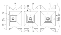
複数の光源20は、複数の開口領域S7、S8に位置する導体配線50の一部の上面に接合部材60を介して接合される。
リフレクタ30は、光源20から出射される光を反射する部材である。リフレクタ30は、光源20からの出射光に対する反射率が、440nm~630nmの領域で平均70%以上であることが好ましい。リフレクタ30には、例えば、酸化チタン、酸化アルミニウム、酸化ケイ素等の金属酸化物粒子からなる反射材を含有する樹脂を用いて成形された部材や、反射材を含有しない樹脂の表面に反射材が設けられた部材などを用いることができる。
光学部材40は複数の光源20を挟んで基体10と対向するよう配置される。傾斜側面Xの上端から光学部材40までの距離K2は、基体10上面から傾斜側面Xの上端までの距離K1の1/2以下であることが好ましい。このようにすれば、リフレクタ30から光学部材40までの距離に対して、第1包囲部32や第2包囲部34の深さが相対的に深くなり、第1包囲部32や第2包囲部34内における光の多重反射の繰り返し回数を増やすことができる。したがって、光学部材40が配置されている位置における、各包囲部の光密度を高めることができる。
発光装置1は接合部材60を有している。接合部材60は、光源20を基体10及び/又は導体配線50に固定するための部材である。接合部材60の一例としては、絶縁性の樹脂や導電性の部材が挙げられる。光源20をフリップチップ実装する場合は導電性の部材を接合部材60として用いることができる。Au含有合金、Ag含有合金、Pd含有合金、In含有合金、Pb-Pd含有合金、Au-Ga含有合金、Au-Sn含有合金、Sn含有合金、Sn-Cu含有合金、Sn-Cu-Ag含有合金、Au-Ge含有合金、Au-Si含有合金、Al含有合金、Cu-In含有合金、金属とフラックスの混合物等は接合部材60の一例である。
図5Aは実施形態2に係る発光装置の模式的平面図であり、図5Bは、複数の第1包囲部32の位置を理解しやすいよう、図5Aにおいて複数の第1包囲部32を灰色着色部で表示した図である。図5Cは、複数の第2包囲部34の位置を理解しやすいよう、図5Aにおいて複数の第2包囲部34を灰色着色部で表示した図である。図5Dは、複数の第3包囲部36の位置を理解しやすいよう、図5Aにおいて複数の第3包囲部36を灰色着色部で表示した図である。図5Eは図5A中の5E-5E断面図である。図5Fは図5Aの部分拡大図において第1包囲部と第2包囲部と第3包囲部とにおける反射部材の開口領域をそれぞれ灰色着色部で表示した図である。
10 基体
20 光源
22 発光素子
26 封止部材
28 反射層
30 リフレクタ
32 第1包囲部
34 第2包囲部
36 第3包囲部
40 光学部材
50 導体配線
60 接合部材
70 反射部材
D1、D2 包囲部における平面部の光源側端部から光源端部までの距離
H1、H2 基体の上面から傾斜側面の上端までの高さ
K1 基体上面から傾斜側面の上端までの距離
K2 傾斜側面の上端から光学部材までの距離
P 光源が隣接する間隔(ピッチ)
S1、S2、S3 包囲部の開口面積
S7、S8、S9 反射部材が有する開口領域の面積
T リフレクタの厚み
X 傾斜側面
Claims (13)
- 基体と、
前記基体の上面に配置される導体配線と、
前記基体の上面と前記導体配線の上面とを被覆し、前記基体の上面の一部と前記導体配線の上面の一部とが位置する複数の開口領域を備える反射部材と、
前記複数の開口領域に位置する前記導体配線の一部の上面に接合部材を介して接合される複数の光源と、
前記反射部材上に配置され、平面視で前記複数の光源の各々をそれぞれが包囲する複数の包囲部を有し、前記複数の包囲部のそれぞれが上方に向かって広がる傾斜側面を有するリフレクタと、を備え、
前記複数の包囲部は、複数の第1包囲部と、前記複数の第1包囲部を取り囲む複数の第2包囲部とを有し、
平面視において、個々の前記第2包囲部内における前記開口領域の面積は、いずれの前記第1包囲部内における前記開口領域の面積よりも小さい発光装置。 - 前記複数の光源が隣接する間隔は、平面視において均一である請求項1に記載の発光装置。
- 前記第2包囲部の前記傾斜側面の上端で規定される上端開口面積が、前記第1包囲部の前記傾斜側面の上端で規定される上端開口面積よりも小さい請求項1または2に記載の発光装置。
- 前記複数の包囲部は、さらに前記第1包囲部と前記第2包囲部との間に設けられた複数の第3包囲部を有し、
平面視において、前記第3包囲部内における前記開口領域の面積は、前記第1包囲部内における前記開口領域の面積よりも小さく、前記第2包囲部内における前記開口領域の面積よりも大きい、
請求項1から3のいずれかに記載の発光装置。 - 前記光源はバットウィング型の配光特性を有する請求項1から4のいずれかに記載の発光装置。
- 前記光源は、発光素子と、前記発光素子からの光を広配光化させるレンズと、を有する請求項1から5のいずれか1項に記載の発光装置。
- 前記光源は、発光素子と、前記発光素子を被覆する封止部材と、前記封止部材の上方に設けられた反射層と、を有する請求項1から6のいずれか1項に記載の発光装置。
- 前記光源は、発光素子と、前記発光素子の上面に設けられた反射層と、前記発光素子と前記反射層とを被覆する封止部材と、を有する請求項1から6のいずれか1項に記載の発光装置。
- 平面視において、前記開口領域の光源側端部は、前記封止部材の外側に位置する請求項8に記載の発光装置。
- 前記複数の光源を挟んで前記基体と対向するよう配置される透光性の光学部材を備え、
前記傾斜側面の上端から前記光学部材までの距離は、前記基体上面から前記傾斜側面の上端までの距離の1/2以下である請求項1から9のいずれか1項に記載の発光装置。 - 前記光学部材は、誘電体多層膜で形成され、入射する光の一部を反射し、一部を透過するハーフミラーを備える請求項10に記載の発光装置。
- 前記リフレクタは、前記傾斜側面の下端から前記光源に向かって延在する平面部を有し、
前記第2包囲部における前記平面部の前記光源側端部から光源端部までの距離は、前記第1包囲部における前記平面部の前記光源側端部から前記光源端部までの距離よりも小さい請求項1から11のいずれか1項に記載の発光装置。 - 前記基体の上面から前記第2包囲部の傾斜側面の上端までの高さは、前記基体の上面から前記第1包囲部の傾斜側面の上端までの高さより高い請求項1から12のいずれか1項に記載の発光装置。
Priority Applications (3)
| Application Number | Priority Date | Filing Date | Title |
|---|---|---|---|
| JP2018124179A JP7177331B2 (ja) | 2018-06-29 | 2018-06-29 | 発光装置 |
| US16/457,412 US10903193B2 (en) | 2018-06-29 | 2019-06-28 | Light-emitting device |
| US17/125,408 US11646298B2 (en) | 2018-06-29 | 2020-12-17 | Light-emitting device |
Applications Claiming Priority (1)
| Application Number | Priority Date | Filing Date | Title |
|---|---|---|---|
| JP2018124179A JP7177331B2 (ja) | 2018-06-29 | 2018-06-29 | 発光装置 |
Publications (2)
| Publication Number | Publication Date |
|---|---|
| JP2020004895A JP2020004895A (ja) | 2020-01-09 |
| JP7177331B2 true JP7177331B2 (ja) | 2022-11-24 |
Family
ID=69008390
Family Applications (1)
| Application Number | Title | Priority Date | Filing Date |
|---|---|---|---|
| JP2018124179A Active JP7177331B2 (ja) | 2018-06-29 | 2018-06-29 | 発光装置 |
Country Status (2)
| Country | Link |
|---|---|
| US (2) | US10903193B2 (ja) |
| JP (1) | JP7177331B2 (ja) |
Families Citing this family (21)
| Publication number | Priority date | Publication date | Assignee | Title |
|---|---|---|---|---|
| KR102631105B1 (ko) | 2017-08-31 | 2024-01-30 | 니치아 카가쿠 고교 가부시키가이샤 | 발광 장치 |
| JP7177331B2 (ja) * | 2018-06-29 | 2022-11-24 | 日亜化学工業株式会社 | 発光装置 |
| US11302248B2 (en) | 2019-01-29 | 2022-04-12 | Osram Opto Semiconductors Gmbh | U-led, u-led device, display and method for the same |
| DE112020000561A5 (de) | 2019-01-29 | 2021-12-02 | Osram Opto Semiconductors Gmbh | Videowand, treiberschaltung, ansteuerungen und verfahren derselben |
| US11271143B2 (en) | 2019-01-29 | 2022-03-08 | Osram Opto Semiconductors Gmbh | μ-LED, μ-LED device, display and method for the same |
| US11610868B2 (en) | 2019-01-29 | 2023-03-21 | Osram Opto Semiconductors Gmbh | μ-LED, μ-LED device, display and method for the same |
| US11156759B2 (en) | 2019-01-29 | 2021-10-26 | Osram Opto Semiconductors Gmbh | μ-LED, μ-LED device, display and method for the same |
| WO2020165185A1 (de) | 2019-02-11 | 2020-08-20 | Osram Opto Semiconductors Gmbh | Optoelektronisches bauelement, optoelektronische anordnung und verfahren |
| US11538852B2 (en) | 2019-04-23 | 2022-12-27 | Osram Opto Semiconductors Gmbh | μ-LED, μ-LED device, display and method for the same |
| JP7604394B2 (ja) | 2019-04-23 | 2024-12-23 | エイエムエス-オスラム インターナショナル ゲーエムベーハー | Ledモジュール、ledディスプレイモジュール、および当該モジュールを製造する方法 |
| JP7608368B2 (ja) | 2019-05-13 | 2025-01-06 | エイエムエス-オスラム インターナショナル ゲーエムベーハー | マルチチップ用キャリア構造体 |
| CN114144727A (zh) | 2019-05-23 | 2022-03-04 | 奥斯兰姆奥普托半导体股份有限两合公司 | 照明装置、导光装置和方法 |
| US11804580B2 (en) * | 2019-11-04 | 2023-10-31 | Sharp Kabushiki Kaisha | Lighting device and method of producing light source substrate |
| JP7332895B2 (ja) * | 2020-01-31 | 2023-08-24 | 日亜化学工業株式会社 | 面状光源の製造方法、面状光源、および光源 |
| CN111352274A (zh) * | 2020-03-18 | 2020-06-30 | 深圳市隆利科技股份有限公司 | 柔性直下式背光模组的制备方法及其装置 |
| JP7144694B2 (ja) * | 2020-07-31 | 2022-09-30 | 日亜化学工業株式会社 | 発光モジュール、面状光源、液晶表示装置 |
| CN114578614B (zh) * | 2020-11-30 | 2025-01-03 | 华为技术有限公司 | 一种背光模组及显示屏 |
| WO2023039855A1 (zh) * | 2021-09-17 | 2023-03-23 | 瑞仪(广州)光电子器件有限公司 | 反射片、背光模组及显示装置 |
| JP2023077024A (ja) | 2021-11-24 | 2023-06-05 | 日亜化学工業株式会社 | 面状光源 |
| WO2024002827A1 (en) * | 2022-06-28 | 2024-01-04 | Signify Holding B.V. | An insert for a light emitting device |
| CN116974109A (zh) * | 2023-08-01 | 2023-10-31 | 上海天马微电子有限公司 | 直下式背光模组、背光模组设计方法及显示装置 |
Citations (8)
| Publication number | Priority date | Publication date | Assignee | Title |
|---|---|---|---|---|
| JP2001257381A (ja) | 2000-03-13 | 2001-09-21 | Sharp Corp | 発光ダイオードおよびその製造方法並びに照明装置 |
| JP2006013265A (ja) | 2004-06-28 | 2006-01-12 | Kyocera Corp | 発光装置およびそれを用いた照明装置 |
| JP2010123570A (ja) | 2008-10-22 | 2010-06-03 | Toshiba Lighting & Technology Corp | 照明器具 |
| WO2012005061A1 (ja) | 2010-07-07 | 2012-01-12 | シャープ株式会社 | バックライトユニット |
| JP2012248769A (ja) | 2011-05-30 | 2012-12-13 | Sharp Corp | 発光装置および表示装置 |
| US20130051017A1 (en) | 2011-02-23 | 2013-02-28 | The Sloan Company, Inc. Dba Sloanled | Led based down light |
| JP2013149711A (ja) | 2012-01-18 | 2013-08-01 | Citizen Holdings Co Ltd | 半導体発光装置 |
| JP2018045972A (ja) | 2016-09-16 | 2018-03-22 | 日亜化学工業株式会社 | 発光装置 |
Family Cites Families (20)
| Publication number | Priority date | Publication date | Assignee | Title |
|---|---|---|---|---|
| US8080828B2 (en) | 2006-06-09 | 2011-12-20 | Philips Lumileds Lighting Company, Llc | Low profile side emitting LED with window layer and phosphor layer |
| EP1895602B1 (en) | 2006-08-29 | 2019-01-23 | Toshiba Lighting & Technology Corporation | Illumination apparatus having a plurality of semiconductor light-emitting devices |
| JP2011181219A (ja) | 2010-02-26 | 2011-09-15 | Toshiba Corp | 光源、面光源モジュールおよび光源の製造方法 |
| WO2012023459A1 (ja) | 2010-08-20 | 2012-02-23 | シャープ株式会社 | 照明装置、表示装置及びテレビ受信装置 |
| US20120147589A1 (en) | 2010-12-14 | 2012-06-14 | Todd Farmer | System for Providing a Directional LED Array |
| US9882094B2 (en) | 2011-03-14 | 2018-01-30 | Intellectual Discovery Co., Ltd. | Light source with inner and outer bodies comprising three different encapsulants |
| EP2704221A4 (en) | 2011-04-28 | 2014-10-15 | Asahi Rubber Inc | SEMICONDUCTOR ELEMENT WITH A LENS AND METHOD OF MANUFACTURING THEREOF |
| US9228715B2 (en) | 2012-02-22 | 2016-01-05 | Avago Technologies General Ip (Singapore) Pte. Ltd. | Hybrid canopy lighting for optimum light beam shaping |
| US9874322B2 (en) | 2012-04-10 | 2018-01-23 | Cree, Inc. | Lensed troffer-style light fixture |
| JP5999983B2 (ja) | 2012-05-28 | 2016-09-28 | シャープ株式会社 | 照明装置および表示装置 |
| JP2013247092A (ja) | 2012-05-29 | 2013-12-09 | Sharp Corp | 発光装置、照明装置、および表示装置 |
| ES2435501B1 (es) | 2013-10-21 | 2014-05-28 | Simon, S.A.U. | Luminaria |
| KR102319111B1 (ko) | 2015-03-30 | 2021-11-01 | 삼성디스플레이 주식회사 | 발광 소자 |
| EP3154096B1 (en) | 2015-10-08 | 2021-03-17 | Nichia Corporation | Light emitting device, integrated light emitting device and light emitting module comprising the same |
| JP6506899B2 (ja) | 2015-10-08 | 2019-04-24 | 日亜化学工業株式会社 | 発光装置、集積型発光装置および発光モジュール |
| JP6299811B2 (ja) | 2015-11-04 | 2018-03-28 | 日亜化学工業株式会社 | 発光装置 |
| US10274168B2 (en) * | 2016-07-20 | 2019-04-30 | Nichia Corporation | Light emitting device |
| JP6868388B2 (ja) * | 2016-12-26 | 2021-05-12 | 日亜化学工業株式会社 | 発光装置および集積型発光装置 |
| KR102631105B1 (ko) * | 2017-08-31 | 2024-01-30 | 니치아 카가쿠 고교 가부시키가이샤 | 발광 장치 |
| JP7177331B2 (ja) * | 2018-06-29 | 2022-11-24 | 日亜化学工業株式会社 | 発光装置 |
-
2018
- 2018-06-29 JP JP2018124179A patent/JP7177331B2/ja active Active
-
2019
- 2019-06-28 US US16/457,412 patent/US10903193B2/en active Active
-
2020
- 2020-12-17 US US17/125,408 patent/US11646298B2/en active Active
Patent Citations (8)
| Publication number | Priority date | Publication date | Assignee | Title |
|---|---|---|---|---|
| JP2001257381A (ja) | 2000-03-13 | 2001-09-21 | Sharp Corp | 発光ダイオードおよびその製造方法並びに照明装置 |
| JP2006013265A (ja) | 2004-06-28 | 2006-01-12 | Kyocera Corp | 発光装置およびそれを用いた照明装置 |
| JP2010123570A (ja) | 2008-10-22 | 2010-06-03 | Toshiba Lighting & Technology Corp | 照明器具 |
| WO2012005061A1 (ja) | 2010-07-07 | 2012-01-12 | シャープ株式会社 | バックライトユニット |
| US20130051017A1 (en) | 2011-02-23 | 2013-02-28 | The Sloan Company, Inc. Dba Sloanled | Led based down light |
| JP2012248769A (ja) | 2011-05-30 | 2012-12-13 | Sharp Corp | 発光装置および表示装置 |
| JP2013149711A (ja) | 2012-01-18 | 2013-08-01 | Citizen Holdings Co Ltd | 半導体発光装置 |
| JP2018045972A (ja) | 2016-09-16 | 2018-03-22 | 日亜化学工業株式会社 | 発光装置 |
Also Published As
| Publication number | Publication date |
|---|---|
| US20200006297A1 (en) | 2020-01-02 |
| US11646298B2 (en) | 2023-05-09 |
| US20210104502A1 (en) | 2021-04-08 |
| JP2020004895A (ja) | 2020-01-09 |
| US10903193B2 (en) | 2021-01-26 |
Similar Documents
| Publication | Publication Date | Title |
|---|---|---|
| JP7177331B2 (ja) | 発光装置 | |
| JP7381974B2 (ja) | 発光装置 | |
| JP7125636B2 (ja) | 発光装置 | |
| JP7522529B2 (ja) | 発光装置 | |
| JP6493345B2 (ja) | 発光装置 | |
| RU2717381C2 (ru) | Светоизлучающее устройство, интегрированное светоизлучающее устройство и светоизлучающий модуль | |
| JP2018107279A (ja) | 発光装置および集積型発光装置 | |
| JP2006066657A (ja) | 発光装置および照明装置 | |
| JP6575507B2 (ja) | 発光装置および集積型発光装置 | |
| JP7014966B2 (ja) | 発光装置 | |
| JP4938255B2 (ja) | 発光素子収納用パッケージ、光源および発光装置 | |
| JP4557613B2 (ja) | 発光素子収納用パッケージ、発光装置および照明装置 | |
| JP7144683B2 (ja) | 発光装置 | |
| JP2005310911A (ja) | 発光素子収納用パッケージおよび発光装置ならびに照明装置 | |
| JP4659515B2 (ja) | 発光素子搭載用基板,発光素子収納用パッケージ,発光装置および照明装置 | |
| JP7189464B2 (ja) | 発光装置 | |
| JP6923832B2 (ja) | 発光装置 | |
| JP7212296B2 (ja) | 発光装置 | |
| JP7144682B2 (ja) | 発光装置 | |
| JP2019083217A (ja) | 発光装置 |
Legal Events
| Date | Code | Title | Description |
|---|---|---|---|
| A621 | Written request for application examination |
Free format text: JAPANESE INTERMEDIATE CODE: A621 Effective date: 20210603 |
|
| A977 | Report on retrieval |
Free format text: JAPANESE INTERMEDIATE CODE: A971007 Effective date: 20220418 |
|
| A131 | Notification of reasons for refusal |
Free format text: JAPANESE INTERMEDIATE CODE: A131 Effective date: 20220510 |
|
| A521 | Request for written amendment filed |
Free format text: JAPANESE INTERMEDIATE CODE: A523 Effective date: 20220708 |
|
| TRDD | Decision of grant or rejection written | ||
| A01 | Written decision to grant a patent or to grant a registration (utility model) |
Free format text: JAPANESE INTERMEDIATE CODE: A01 Effective date: 20221011 |
|
| A61 | First payment of annual fees (during grant procedure) |
Free format text: JAPANESE INTERMEDIATE CODE: A61 Effective date: 20221024 |
|
| R151 | Written notification of patent or utility model registration |
Ref document number: 7177331 Country of ref document: JP Free format text: JAPANESE INTERMEDIATE CODE: R151 |
|
| R250 | Receipt of annual fees |
Free format text: JAPANESE INTERMEDIATE CODE: R250 |