EP3461006A2 - Protection circuit, oscillation compensation circuit and power supply circuit in solid state pulse modulator - Google Patents
Protection circuit, oscillation compensation circuit and power supply circuit in solid state pulse modulator Download PDFInfo
- Publication number
- EP3461006A2 EP3461006A2 EP18190829.4A EP18190829A EP3461006A2 EP 3461006 A2 EP3461006 A2 EP 3461006A2 EP 18190829 A EP18190829 A EP 18190829A EP 3461006 A2 EP3461006 A2 EP 3461006A2
- Authority
- EP
- European Patent Office
- Prior art keywords
- igbt
- voltage
- collector
- circuit
- gate
- Prior art date
- Legal status (The legal status is an assumption and is not a legal conclusion. Google has not performed a legal analysis and makes no representation as to the accuracy of the status listed.)
- Granted
Links
Images



Classifications
-
- H—ELECTRICITY
- H03—ELECTRONIC CIRCUITRY
- H03K—PULSE TECHNIQUE
- H03K17/00—Electronic switching or gating, i.e. not by contact-making and –breaking
- H03K17/08—Modifications for protecting switching circuit against overcurrent or overvoltage
- H03K17/081—Modifications for protecting switching circuit against overcurrent or overvoltage without feedback from the output circuit to the control circuit
- H03K17/08116—Modifications for protecting switching circuit against overcurrent or overvoltage without feedback from the output circuit to the control circuit in composite switches
-
- H—ELECTRICITY
- H03—ELECTRONIC CIRCUITRY
- H03K—PULSE TECHNIQUE
- H03K17/00—Electronic switching or gating, i.e. not by contact-making and –breaking
- H03K17/06—Modifications for ensuring a fully conducting state
-
- H—ELECTRICITY
- H03—ELECTRONIC CIRCUITRY
- H03K—PULSE TECHNIQUE
- H03K17/00—Electronic switching or gating, i.e. not by contact-making and –breaking
- H03K17/08—Modifications for protecting switching circuit against overcurrent or overvoltage
- H03K17/081—Modifications for protecting switching circuit against overcurrent or overvoltage without feedback from the output circuit to the control circuit
- H03K17/0812—Modifications for protecting switching circuit against overcurrent or overvoltage without feedback from the output circuit to the control circuit by measures taken in the control circuit
- H03K17/08126—Modifications for protecting switching circuit against overcurrent or overvoltage without feedback from the output circuit to the control circuit by measures taken in the control circuit in bipolar transitor switches
-
- H—ELECTRICITY
- H03—ELECTRONIC CIRCUITRY
- H03K—PULSE TECHNIQUE
- H03K17/00—Electronic switching or gating, i.e. not by contact-making and –breaking
- H03K17/08—Modifications for protecting switching circuit against overcurrent or overvoltage
- H03K17/081—Modifications for protecting switching circuit against overcurrent or overvoltage without feedback from the output circuit to the control circuit
- H03K17/0812—Modifications for protecting switching circuit against overcurrent or overvoltage without feedback from the output circuit to the control circuit by measures taken in the control circuit
- H03K17/08128—Modifications for protecting switching circuit against overcurrent or overvoltage without feedback from the output circuit to the control circuit by measures taken in the control circuit in composite switches
-
- H—ELECTRICITY
- H03—ELECTRONIC CIRCUITRY
- H03K—PULSE TECHNIQUE
- H03K17/00—Electronic switching or gating, i.e. not by contact-making and –breaking
- H03K17/51—Electronic switching or gating, i.e. not by contact-making and –breaking characterised by the components used
- H03K17/56—Electronic switching or gating, i.e. not by contact-making and –breaking characterised by the components used by the use, as active elements, of semiconductor devices
- H03K17/567—Circuits characterised by the use of more than one type of semiconductor device, e.g. BIMOS, composite devices such as IGBT
-
- H—ELECTRICITY
- H03—ELECTRONIC CIRCUITRY
- H03K—PULSE TECHNIQUE
- H03K3/00—Circuits for generating electric pulses; Monostable, bistable or multistable circuits
- H03K3/02—Generators characterised by the type of circuit or by the means used for producing pulses
- H03K3/53—Generators characterised by the type of circuit or by the means used for producing pulses by the use of an energy-accumulating element discharged through the load by a switching device controlled by an external signal and not incorporating positive feedback
- H03K3/57—Generators characterised by the type of circuit or by the means used for producing pulses by the use of an energy-accumulating element discharged through the load by a switching device controlled by an external signal and not incorporating positive feedback the switching device being a semiconductor device
-
- H—ELECTRICITY
- H03—ELECTRONIC CIRCUITRY
- H03K—PULSE TECHNIQUE
- H03K17/00—Electronic switching or gating, i.e. not by contact-making and –breaking
- H03K17/06—Modifications for ensuring a fully conducting state
- H03K2017/066—Maximizing the OFF-resistance instead of minimizing the ON-resistance
-
- H—ELECTRICITY
- H03—ELECTRONIC CIRCUITRY
- H03K—PULSE TECHNIQUE
- H03K2217/00—Indexing scheme related to electronic switching or gating, i.e. not by contact-making or -breaking covered by H03K17/00
- H03K2217/0081—Power supply means, e.g. to the switch driver
Definitions
- the present disclosure generally relates to the field of electronic technology, and more particularly, to a gate protection circuit, an oscillation compensation circuit, an overcurrent protection circuit, and an overvoltage protection circuit for an Insulated Gate Bipolar Transistor (IGBT), a power supply circuit for a solid state pulse modulator based on the MARX generator principle, and a solid state pulse modulator based on the MARX generator principle including one or more of the above circuits.
- IGBT Insulated Gate Bipolar Transistor
- a solid state pulse modulator based on the MARX generator principle uses an IGBT as a switch element, and turn-on and turn-off of the IGBT is controlled by a gate voltage.
- the IGBT is turned on when a positive voltage is applied to a gate of the IGBT, and the IGBT is turned off when a negative voltage is applied to the gate.
- the reliability of the IGBT is very important for the solid state pulse modulator.
- the safety and reliability of the IGBT is determined, at least in part, by a voltage between the gate and an emitter of the IGBT, a voltage between a collector and the emitter of the IGBT, current flowing through the collector-emitter of the IGBT, and a junction temperature of the IGBT, etc..
- the IGBT cannot operate stably and normally.
- the voltage is too high to exceed a withstand voltage between the gate and the emitter, the IGBT may be permanently damaged.
- the voltage applied between the collector and the emitter of the IGBT exceeds the withstand voltage between the collector and the emitter, or the current flowing through the collector-emitter of the IGBT exceeds maximum allowed current between the collector and the emitter, or the junction temperature of the IGBT exceeds an allowable value of its junction temperature, the IGBT may be permanently damaged.
- the present disclosure aims to at least partially solve the problems of gate protection, oscillation compensation, overcurrent protection or overvoltage protection etc. of various stages of IGBT switches in a solid state pulse modulator based on the MARX generator principle, so as to ensure that the solid state pulse modulator operates stably and reliably.
- a solid state pulse modulator based on the MARX generator principle comprising a gate protection circuit for an Insulated Gate Bipolar Transistor (IGBT), the IGBT being used as a switch device in a solid state pulse modulator based on the MARX generator principle, the gate protection circuit comprising: a voltage regulator configured to supply a stable voltage to an emitter of the IGBT with respect to the ground for a gate of the IGBT.
- IGBT Insulated Gate Bipolar Transistor
- the voltage regulator is a voltage regulation diode having a cathode connected to an emitter of the IGBT, and an anode connected to the ground for the gate of the IGBT.
- the solid state pulse modulator further comprises an oscillation compensation circuit for the IGBT, the oscillation compensation circuit comprising:
- the solid state pulse modulator further comprises an overcurrent protection circuit for the IGBT, the overcurrent protection circuit comprising:
- the overcurrent trigger signal is input to the driving circuit through an AND gate together with a gate control trigger signal of the IGBT, and
- the overcurrent trigger circuit when the signal output by the collector voltage detection circuit indicates that the voltage at the collector exceeds the reference value, the overcurrent trigger circuit outputs the overcurrent trigger signal at a low level.
- the overcurrent trigger circuit comprises a transistor having a first terminal connected to an input terminal of the AND gate, and a second terminal connected to a low level, and
- the transistor in response to the signal output by the collector voltage detection circuit indicating that the voltage at the collector exceeds the reference value, the transistor is turned on to turn on a connection between the first terminal and the second terminal.
- the collector voltage detection circuit is configured to detect the voltage at the collector for a predetermined time after a time at which the IGBT starts to be turned on.
- the collector voltage detection circuit comprises:
- the delay mechanism comprises a capacitor, wherein an output terminal of the constant current source is connected on the one hand to a first terminal of the capacitor and on the other hand to the collector of the IGBT via a detection resistor, wherein a second terminal of the capacitor is connected to a ground potential, and wherein there is a unidirectional conduction device between the constant current source and the collector, so that the capacitor can only be charged by the current from the constant current source.
- the collector voltage detection circuit further comprises: a voltage regulation diode and a resistor connected between the first terminal of the capacitor and the ground potential, and wherein a connection node between the voltage regulation diode and the resistor is used as an output node of the collector voltage detection circuit.
- the solid state pulse modulator further comprises an overvoltage protection circuit for the IGBT, the overvoltage protection circuit comprising:
- the solid state pulse modulator further comprises an additional overvoltage protection branch configured to output to the gate of the IGBT a signal for causing the IGBT to be turned on when the signal output by the collector voltage detection circuit indicates that the voltage at the collector exceeds the reference value.
- the solid state pulse modulator further comprises a power supply circuit for a driving circuit of the IGBT, comprising:
- the conductive wire passes through the mutual inductance coil.
- Fig. 1 illustrates a schematic circuit diagram of a solid state pulse modulator according to an embodiment of the present disclosure.
- the solid state pulse modulator may comprise a plurality of (for example, 11, depending on pulse voltages required) charging and discharging modules 100, and each of the charging and discharging modules 100 may comprise a capacitor 1001, an IGBT 1002 and diode 1003.
- a first terminal of the capacitor 1001 is connected to a collector of the IGBT, and a second terminal of the capacitor 1001 is connected to an emitter of the IGBT via the diode 1003.
- a gate of the IGBT is connected to a driving circuit (not shown) to be turned on or turned off according to a driving signal from the driving circuit, and accordingly a connection configuration of the capacitors in various charging and discharging modules 100 is changed accordingly.
- the plurality of charging and discharging modules are connected in parallel via diodes.
- a first charging and discharging module 100 is connected to a capacitor 1004, and a last charging and discharging module 100 is connected in parallel with another IGBT 1002 via a diode.
- all IGBTs are turned off in a charging process, so that all capacitors are connected in parallel, and a voltage across each capacitor may be a power supply voltage for charging, for example, 750V, all IGBTs are turned on in a discharging process, so that various capacitors are connected in series via the IGBTs, and thus the voltages across the capacitors may be added to provide a high voltage to the outside.
- a voltage across each capacitor may be a power supply voltage for charging, for example, 750V
- all IGBTs are turned on in a discharging process, so that various capacitors are connected in series via the IGBTs, and thus the voltages across the capacitors may be added to provide a high voltage to the outside.
- Fig. 2 illustrates a schematic circuit diagram of a gate protection circuit for an IGBT according to an embodiment of the present disclosure.
- the gate protection circuit comprises a voltage regulator 201 which may supply a stable voltage to an emitter E of the IGBT with respect to the ground for a gate G of the IGBT.
- the voltage regulator may be a voltage regulation diode 2001.
- a cathode of the voltage regulation diode 2001 is connected to the emitter E of the IGBT, and an anode of the voltage regulation diode is connected to the ground for the gate G of the IGBT.
- the voltage regulation diode 2001 is connected in reverse between a positive power supply and the ground for the gate (e.g., via a resistor 2002).
- the gate of the IGBT is grounded during a period in which the IGBT needs to be turned off. Therefore, the voltage regulation diode 2001 is reversely broken down, and thus a constant voltage such as 5V is maintained between the emitter and the gate (at this time, a ground potential).
- the voltage between the gate and the emitter may be set to a stable negative voltage (for example, -5V). This negative bias can prevent the IGBT from being mis-turned on due to excessive surge current when the IGBT is turned off.
- Turn-on resistance of the IGBT decreases when a forward driving voltage increases, to reduce a turn-on loss.
- the forward driving voltage is too large, the gate may easily be damaged, and therefore it is necessary to appropriately select the forward driving voltage of the voltage regulation diode 2001, for example, 15V.
- the driving circuit should provide sufficient voltage and current amplitude to prevent the IGBT from being damaged due to being out of a saturation turn-on region under normal operation and overload conditions.
- the gate protection circuit may further comprise a resistor 3033 connected between the gate G and the emitter E, as shown in Fig. 3 .
- the gate protection circuit may further comprise a TVP tube 3034 connected between the gate G and the emitter E, as shown in Fig. 3 . As mentioned above, a stable voltage of 15V may be provided across the TVP tube 3034.
- fast turn-on and turn-off of the IGBT facilitates reducing switch losses. Since the solid state modulator has a very short pulse width (usually only a few us), in the solid state modulator, turn-on and turn-off of the IGBT needs to be performed as fast as possible. Junction capacitance of the gate of the IGBT is usually large, and large driving current is required in order to achieve fast turn-on and turn-off.
- the driving circuit of the IGBT may comprise a driving signal generator 301 and an amplification stage 302.
- the driving signal generator 301 may generate a driving signal (driving pulse) for the IGBT according to a received gate control trigger signal (input at a terminal 4).
- the driving signal generator 301 may comprise a dedicated trigger chip IXDN 604 (reference numerals 2, 3, 4, 5, 6, 7 in Fig. 3 indicate respective pins of the IXDN 604).
- the amplification stage 302 may amplify the driving signal (e.g., amplify current to achieve large driving current).
- the amplification stage 302 may comprise an amplification device such as a triode in a push-pull configuration.
- the triode may also facilitate the access of an overvoltage protection circuit described below.
- the driving current of the driving circuit may be large, and internal resistance of the driving circuit may be less than 1 ohm.
- an oscillation compensation circuit 303 may be provided to at least partially suppress such oscillation.
- Fig. 3 illustrates a schematic circuit diagram of an oscillation compensation circuit for an IGBT according to an embodiment of the present disclosure.
- the oscillation compensation circuit 303 may comprise an oscillation suppression resistor 3031 connected in series to a gate of the IGBT and an oscillation suppression capacitor 3032 connected in parallel between the gate and an emitter E of the IGBT.
- a driving signal of the IGBT is input to the gate G of the IGBT via the oscillation suppression resistor 3031, and the oscillation suppression capacitor 3032 is connected between the gate G and the emitter E of the IGBT.
- Selecting appropriate oscillation suppression resistor 3031 and oscillation suppression capacitor 3032 is advantageous for suppressing oscillation without increasing switching time and switching loss of the IGBT.
- junction capacitance of the IGBT used in the solid state modulator is about tens of nF
- the distributed inductance in the driving circuit is about tens of nH
- other internal resistance in the driving circuit is about 1 ohm.
- R G may be selected as 1 ohm
- C G may be selected as 47nF
- a trigger rising edge is about several hundreds of ns.
- the overcurrent protection circuit of the IGBT adopts a soft turn-off scheme, since the fast turn-off of the gate voltage may cause the IGBT to be "locked” and cannot be turned off when severe overcurrent of the IGBT happens.
- the gate voltage requires a reduction process for tens of us to form slow turn-off.
- hard turn-off may be used.
- a turn-on voltage drop of the IGBT is very low when the IGBT is normally turned on, and the turn-on voltage drop increases when overcurrent of the IGBT happens. Therefore, the turn-on voltage drop may be detected in the turn-on process, and it may be determined whether overcurrent of the IGBT happens.
- 4a illustrates a schematic structural diagram of an overcurrent protection circuit for an IGBT according to an embodiment of the present disclosure.
- the overcurrent protection circuit may comprise a collector voltage detection circuit 401 and an overcurrent trigger circuit 402.
- the collector voltage detection circuit 401 may detect a voltage at a collector of the IGBT during a turn-on phase of the IGBT, and output a signal indicating whether the voltage at the collector exceeds a reference value. According to an embodiment of the present disclosure, the detection of the voltage at the collector by the collector voltage detection circuit 401 may be started after a period of time (for example, 1 to 2 us) after the IGBT is turned on, because the voltage drop is relatively large when the IGBT is just turned on. It is easy to cause the collector voltage detection circuit 401 to detect a high voltage and thus cause malfunction of the overcurrent protection circuit.
- the overcurrent trigger circuit 402 may output an overcurrent trigger signal to the driving circuit of the IGBT when a signal output by the collector voltage detection circuit indicates that the voltage at the collector exceeds the reference value, so that the driving circuit outputs to the gate of the IGBT a driving signal which causes the IGBT to be turned off.
- the driving circuit may receive two control signals, wherein one of the control signals is a gate control trigger signal which normally controls the IGBT to be turned on/off, and the other of the control signals is the above-described overcurrent trigger signal.
- the overcurrent trigger signal may be input to the driving circuit 404 via an AND gate 403 along with the gate control trigger signal of the IGBT.
- the overcurrent trigger signal is input to a terminal 2 of an AND gate 4031
- the gate control trigger signal is input to a terminal 1 of the AND gate 4031.
- the overcurrent trigger circuit may output an overcurrent trigger signal at a low level when the signal output by the collector voltage detection circuit 401 indicates that the voltage at the collector exceeds the reference value. Due to the action of the AND gate, even if the gate control trigger signal is high (used to drive the IGBT to be turned on), the input of the driving signal is set to be low, thereby turning off the voltage at the gate G. Thus, the current path is disconnected, thereby achieving overcurrent protection.
- the overcurrent trigger circuit 402 may selectively output a low level signal according to an output of the collector voltage detection circuit 401.
- the overcurrent trigger circuit 402 may comprise a switch device such as a field effect transistor 4021, which has a gate controlled by the output of the collector voltage detection circuit 401 to selectively connect the terminal 2 of the AND gate 4031 to the ground.
- a first terminal of the transistor 4021 is connected to an input terminal of the AND gate 403, for example, the terminal 2 of the AND gate 4031, and a second terminal of the transistor 4021 is connected to a low level.
- the transistor 4021 In response to the signal output by the collector voltage detection circuit 401 indicating that the voltage at the collector exceeds a reference value (e.g., a high level applied to the gate of the field effect transistor 4021), the transistor 4021 is turned on, to turn on a connection between the first terminal and the second terminal, and thus connecting the first terminal (i.e., the input terminal of the AND gate 4031) to the ground.
- a reference value e.g., a high level applied to the gate of the field effect transistor 4021
- detection current may be supplied to the collector (via a resistor) to perform voltage detection.
- the collector voltage detection circuit 401 may comprise a constant current source 4011.
- the constant current source 4011 may start up (i.e., starting up in synchronization with the turn-on of the IGBT) in response to a driving signal in the driving circuit 404 which causes the IGBT to be turned on to generate constant detection current.
- the constant current source 4011 may comprise a transistor 4011-1.
- a voltage regulation diode 4011-2 and a resistor 4011-3 are connected between a gate and a drain of the transistor.
- the driving signal is high (indicating that the IGBT is turned on)
- the voltage regulation diode 4011-2 may be reversely broken down and thus a constant voltage is maintained across the voltage regulation diode 4011-2.
- This constant voltage produces constant emitter current via the resistor 4011-3, and thus substantially constant current may be output by the collector for use as the detection current.
- the configuration of the constant current source is not limited thereto.
- the collector voltage detection circuit 401 may further comprise a delay mechanism 4012.
- the delay mechanism 4012 causes the constant current generated by the constant current source 4011 to be supplied to the collector C of the IGBT when a predetermined time elapses after the constant current source starts up.
- the delay mechanism 4012 may comprise a capacitor, such as a capacitor 4012-1 shown in Fig. 4b .
- a capacitor such as a capacitor 4012-1 shown in Fig. 4b .
- an output terminal of the constant current source 4011 is connected to a first terminal of the capacitor on the one hand and to the collector C of the IGBT via a detection resistor 405 on the other hand.
- a second terminal of the capacitor 4012-1 may be connected to the ground potential.
- There is a unidirectional conduction device such as a diode 406 between the constant current source 4011 and the collector C, so that the capacitor can only be charged by the current from the constant current source (thereby, for example, preventing the collector C from charging the capacitor 4012-1 when there is a high voltage at the collector C).
- the voltage at P1 gradually increases.
- the voltage at the collector decreases (close to the voltage at the emitter).
- the detection current may flow into the collector C. That is, the detection current is delayed by the time required for the voltage at P1 to increase to be above the voltage at the collector.
- the voltage at P1 is approximately the voltage at the collector + the detection current *R1, where R1 represents a resistance value of the resistor 405.
- a current value of the detection current, a resistance value of the resistor 405, and parameters of the voltage regulation diode 407 may be selected so that the voltage regulation diode 407 is not reversely broken down at this time, and thus the input at the terminal 2 of the AND gate 4031 is maintained at a high level.
- the voltage at the collector may increase. Due to the presence of the unidirectional conduction device 406, the detection current may further charge the capacitor 4012-1 and thus the voltage at P1 increases. Finally, the voltage at P1 may cause the voltage regulation diode 407 to be reversely broken down and thus a constant voltage is maintained across the voltage regulation diode 407. The presence of this voltage may cause the transistor 4021 to be turned on, and thus pull down the input at the terminal 2 of the AND gate 4031 to the ground potential. In response to this low input, the driving circuit may cause the IGBT to be turned off.
- the collector voltage detection circuit 401 converts a high voltage and a low voltage at the collector to a high level signal and a low level signal by the voltage regulation diode 407 and the resistor 408 connected between the first terminal of the capacitor 4012-1 and the ground potential.
- the high level signal and the low level signal are output at a connection node between the voltage regulation diode 407 and the resistor 408 to control the overcurrent trigger circuit 402.
- the present disclosure is not limited thereto. There are various techniques in the art to convert the high voltage and low voltage at P1 into corresponding high and low level control signals, respectively.
- the IGBT in the solid state modulator needs to be turned off quickly, and a high surge spike voltage U CE may be generated between the collector C and the emitter E of the IGBT due to the action of stray inductance and load inductance in the circuit.
- the overvoltage resistance of the IGBT is poor, which may cause the IGBT to be broken down. Therefore, overvoltage protection of the IGBT is also very important.
- a method of reducing the voltage U CE between the collector and the emitter of the IGBT may be to increase resistance R G of the gate. However, the increase of R G may slow down the turn-on/off speed of the IGBT, thereby increasing the turn-on/off loss. Accordingly, this method is not ideal.
- Fig. 5a illustrates an overvoltage protection circuit for an IGBT according to an embodiment of the present disclosure.
- the overvoltage protection circuit may comprise a collector voltage detection circuit 501 and an overvoltage trigger circuit 502.
- the collector voltage detection circuit 501 may detect a voltage at a collector of the IGBT during a turn-off phase of the IGBT, and output a signal indicating whether the voltage at the collector exceeds a reference value.
- the reference value may be, for example, 750V depending on actual needs.
- the collector voltage detection circuit 501 may comprise one or more TVP tubes connected in series, as shown in Fig. 5b .
- a number of the TVP tubes may be determined according to the above reference value, for example, the number of the TVP tubes is 3 in a case that the reference value is 750V. In this case, during the turn-off phase of the IGBT, when the voltage at the collector is too high (surge voltage), the collector voltage detection circuit 501 may output a high level signal.
- the overvoltage trigger circuit 502 may output an overvoltage trigger signal to a driving circuit 503 of the IGBT when the signal output by the collector voltage detection circuit 501 indicates that the voltage at the collector exceeds the reference value, so that the driving circuit 503 outputs to a gate of the IGBT a driving signal which causes the IGBT to be turned on.
- an output terminal of the overvoltage trigger circuit 502 may be connected to a control terminal of a high side transistor (e.g., 5001 shown in Fig. 5b ) of a driving current amplifier circuit in push-pull configuration in the driving circuit 503 of the IGBT.
- a high side transistor e.g., 5001 shown in Fig. 5b
- the overvoltage trigger circuit 502 may output a high level signal to cause the high side transistor to be turned on, and thus output to the gate of the IGBT a driving signal for driving the IGBT to be turned on.
- the overvoltage trigger circuit 502 may output a high level signal to cause the high side transistor to be turned on, and thus output to the gate of the IGBT a driving signal for driving the IGBT to be turned on.
- the overvoltage trigger circuit 502 may simply connect an output node of the collector voltage detection circuit 501 (via a resistor) to a gate of the high side transistor.
- the gate of the IGBT may be turned on to release a certain amount of electrical energy to form appropriate slow turn-off.
- the IGBT when the voltage at the collector exceeds a voltage of the TVP tube, current flows through the TVP tube, is amplified by the triode and is then applied to the gate of the IGBT, the IGBT is turned on to release the electrical energy, and then the voltage of the IGBT decreases.
- the gate is turned off. In this way, adaptive slow turn-off is formed to achieve overvoltage protection.
- an additional overvoltage protection branch may also be provided.
- the overvoltage protection branch may output a signal which causes the IGBT to be turned on to the gate of the IGBT when the signal output by the collector voltage detection circuit indicates that the voltage at the collector exceeds the reference value.
- the additional overvoltage protection branch may simply connect the output node of the collector voltage detection circuit 501 to the gate of the IGBT (via a resistor).
- the MARX discharge loop is employed, various IGBT modules are floated differently at different high voltages, and both triggering and power supply for the triggering need to be isolated.
- the triggering may be transmitted through an optical fiber, and the power supply for the triggering may be realized using a method for coupling high-frequency current with a current transformer, may be transmitted through a high-voltage-resistant wire, wherein a primary transformer may be implemented using a 1-turn transformer.
- Fig. 6 illustrates a schematic circuit diagram of a power supply circuit for an IGBT in a solid state pulse modulator based on MARX generator principle according to an embodiment of the present disclosure.
- the power supply circuit may comprise a mutual inductance coil 601, a conductive wire, a bridge rectifier 602, and a voltage regulation diode 603.
- the conductive wire is coupled to the mutual inductance coil and passes through the mutual inductance coil for transmitting alternating current and thus generating an alternating current signal in the mutual inductance coil.
- the bridge rectifier 602 converts the alternating current signal into a direct current signal to power a driving circuit.
- a positive output terminal 3 of the bridge rectifier 602 provides a power supply voltage and a negative output terminal 4 of the bridge rectifier 602 is connected to the ground for a gate of the IGBT.
- the voltage regulation diode 603 is connected between the positive output terminal and the negative output terminal of the rectifier.
- the present disclosure further provides a solid state pulse modulator based on the MARX generator principle, comprising one or more of the gate protection circuit, the oscillation compensation circuit, the overcurrent protection circuit, the overvoltage protection circuit, and the power supply circuit as described above.
- the present disclosure can ensure the safety and reliability of the IGBT.
- the above described methods, apparatus, units and/or modules in accordance with various embodiments of the present disclosure may be implemented by execution of software comprising computer instructions by a computational electronic device.
- the system may comprise storage devices to implement the various storages described above.
- the computational electronic device may comprise a general purpose processor, a digital signal processor, a dedicated processor, a reconfigurable processor, etc., which can execute computer instructions, but is not limited thereto. Execution of such instructions causes the electronic device to be configured to perform the operations described above in accordance with the present disclosure.
- Each of the above devices and/or modules may be implemented in one electronic device or in different electronic devices.
- the software can be stored in a computer readable storage medium.
- the computer readable storage medium stores one or more programs (software modules), the one or more programs including instructions that, when executed by one or more processors in an electronic device, cause the electronic device to execute methods of the present disclosure.
- the software may be stored in the form of volatile memory or non-volatile storage (e.g., a storage device like a ROM), whether erasable or rewritable, or stored in the form of a memory (e.g., RAM, memory chip, device or integrated circuit) is either stored on an optically readable medium or a magnetically readable medium (e.g., CD, DVD, magnetic disk or magnetic tape, etc.).
- volatile memory e.g., RAM, memory chip, device or integrated circuit
- a magnetically readable medium e.g., CD, DVD, magnetic disk or magnetic tape, etc.
- the embodiment provides a program and a machine readable storage device storing such a program, the program comprising code for implementing the apparatus or method of any of the claims of the present disclosure.
- these programs can be transferred via any medium, such as a communication signal carried via a wired connection or a wireless connection, and various embodiments suitably include such programs.
- Methods, apparatus, units, and/or modules in accordance with various embodiments of the present disclosure may be implemented by, for example, a field programmable gate array (FPGA), a programmable logic array (PLA), a system on a chip, a system on a substrate, a system on a package, an application specific integrated circuit (ASIC), or in hardware or firmware, such as in any other reasonable manner for integrating or encapsulating the circuit, or in a suitable combination of three implementations of software, hardware, and firmware.
- the system may comprise a storage device to implement the storage described above.
- the software, hardware, and/or firmware used is programmed or designed to perform the respective methods, steps and/or functions described above in accordance with the present disclosure.
- One skilled in the art can appropriately implement one or more of these systems and modules, or a part of some parts of them, using different implementations described above, according to actual needs. These implementations fall within the scope of protection of the present disclosure.
Landscapes
- Electronic Switches (AREA)
- Power Conversion In General (AREA)
- Dc-Dc Converters (AREA)
Abstract
Description
- The present disclosure generally relates to the field of electronic technology, and more particularly, to a gate protection circuit, an oscillation compensation circuit, an overcurrent protection circuit, and an overvoltage protection circuit for an Insulated Gate Bipolar Transistor (IGBT), a power supply circuit for a solid state pulse modulator based on the MARX generator principle, and a solid state pulse modulator based on the MARX generator principle including one or more of the above circuits.
- A solid state pulse modulator based on the MARX generator principle uses an IGBT as a switch element, and turn-on and turn-off of the IGBT is controlled by a gate voltage. The IGBT is turned on when a positive voltage is applied to a gate of the IGBT, and the IGBT is turned off when a negative voltage is applied to the gate.
- The reliability of the IGBT is very important for the solid state pulse modulator. The safety and reliability of the IGBT is determined, at least in part, by a voltage between the gate and an emitter of the IGBT, a voltage between a collector and the emitter of the IGBT, current flowing through the collector-emitter of the IGBT, and a junction temperature of the IGBT, etc..
- On the one hand, if the voltage between the gate and the emitter of the IGBT, that is, a driving voltage is too low, the IGBT cannot operate stably and normally. On the other hand, if the voltage is too high to exceed a withstand voltage between the gate and the emitter, the IGBT may be permanently damaged. Similarly, if the voltage applied between the collector and the emitter of the IGBT exceeds the withstand voltage between the collector and the emitter, or the current flowing through the collector-emitter of the IGBT exceeds maximum allowed current between the collector and the emitter, or the junction temperature of the IGBT exceeds an allowable value of its junction temperature, the IGBT may be permanently damaged.
- Therefore, it is necessary to ensure reliability of various stages of IGBT switches in the solid state pulse modulator based on the MARX generator principle, such as gate protection, oscillation compensation, overcurrent protection or overvoltage protection etc.
- The present disclosure aims to at least partially solve the problems of gate protection, oscillation compensation, overcurrent protection or overvoltage protection etc. of various stages of IGBT switches in a solid state pulse modulator based on the MARX generator principle, so as to ensure that the solid state pulse modulator operates stably and reliably.
- According to an aspect of the present disclosure, there is provided a solid state pulse modulator based on the MARX generator principle, comprising a gate protection circuit for an Insulated Gate Bipolar Transistor (IGBT), the IGBT being used as a switch device in a solid state pulse modulator based on the MARX generator principle, the gate protection circuit comprising:
a voltage regulator configured to supply a stable voltage to an emitter of the IGBT with respect to the ground for a gate of the IGBT. - According to an aspect of the present disclosure, the voltage regulator is a voltage regulation diode having a cathode connected to an emitter of the IGBT, and an anode connected to the ground for the gate of the IGBT.
- According to an aspect of the present disclosure, the solid state pulse modulator further comprises an oscillation compensation circuit for the IGBT, the oscillation compensation circuit comprising:
- an oscillation suppression resistor RG, wherein a driving signal of the IGBT is input to a gate of the IGBT via the oscillation suppression resistor; and
- an oscillation suppression capacitor CG connected between the gate and an emitter of the IGBT.
- According to an aspect of the present disclosure, the oscillation suppression resistor RG and the oscillation suppression capacitor CG satisfy the following formula:

- According to an aspect of the present disclosure, the solid state pulse modulator further comprises an overcurrent protection circuit for the IGBT, the overcurrent protection circuit comprising:
- a collector voltage detection circuit configured to detect a voltage at a collector of the IGBT during a turn-on phase of the IGBT, and output a signal indicating whether the voltage at the collector exceeds a reference value; and
- an overcurrent trigger circuit configured to output an overcurrent trigger signal to the driving circuit of the IGBT when the signal output by the collector voltage detection circuit indicates that the voltage at the collector exceeds the reference value, so that the driving circuit outputs to the gate of the IGBT a driving signal which causes the IGBT to be turned off.
- According to an aspect of the present disclosure, the overcurrent trigger signal is input to the driving circuit through an AND gate together with a gate control trigger signal of the IGBT, and
- wherein, when the signal output by the collector voltage detection circuit indicates that the voltage at the collector exceeds the reference value, the overcurrent trigger circuit outputs the overcurrent trigger signal at a low level.
- According to an aspect of the present disclosure, the overcurrent trigger circuit comprises a transistor having a first terminal connected to an input terminal of the AND gate, and a second terminal connected to a low level, and
- wherein, in response to the signal output by the collector voltage detection circuit indicating that the voltage at the collector exceeds the reference value, the transistor is turned on to turn on a connection between the first terminal and the second terminal.
- According to an aspect of the present disclosure, the collector voltage detection circuit is configured to detect the voltage at the collector for a predetermined time after a time at which the IGBT starts to be turned on.
- According to an aspect of the present disclosure, the collector voltage detection circuit comprises:
- a constant current source configured to start up in response to the driving signal in the driving circuit which causes the IGBT to be turned on, to generate constant detection current; and
- a delay mechanism configured to cause the constant detection current generated by the constant current source to be supplied to the collector of the IGBT when a predetermined time elapses after the constant current source starts up.
- According to an aspect of the present disclosure, the delay mechanism comprises a capacitor,
wherein an output terminal of the constant current source is connected on the one hand to a first terminal of the capacitor and on the other hand to the collector of the IGBT via a detection resistor, wherein a second terminal of the capacitor is connected to a ground potential, and
wherein there is a unidirectional conduction device between the constant current source and the collector, so that the capacitor can only be charged by the current from the constant current source. - According to an aspect of the present disclosure, the collector voltage detection circuit further comprises: a voltage regulation diode and a resistor connected between the first terminal of the capacitor and the ground potential, and
wherein a connection node between the voltage regulation diode and the resistor is used as an output node of the collector voltage detection circuit. - According to an aspect of the present disclosure, the solid state pulse modulator further comprises an overvoltage protection circuit for the IGBT, the overvoltage protection circuit comprising:
- a collector voltage detection circuit configured to detect a voltage at a collector of the IGBT during a turn-off phase of the IGBT, and output a signal indicating whether the voltage at the collector exceeds a reference value; and
- an overvoltage trigger circuit configured to output an overvoltage trigger signal to a driving circuit of the IGBT when the signal output by the collector voltage detection circuit indicates that the voltage at the collector exceeds the reference value, so that the driving circuit outputs to a gate of the IGBT a driving signal which causes the IGBT to be turned on.
- According to an aspect of the present disclosure, the solid state pulse modulator further comprises an additional overvoltage protection branch configured to output to the gate of the IGBT a signal for causing the IGBT to be turned on when the signal output by the collector voltage detection circuit indicates that the voltage at the collector exceeds the reference value.
- According to an aspect of the present disclosure, the solid state pulse modulator further comprises a power supply circuit for a driving circuit of the IGBT, comprising:
- a mutual inductance coil;
- a conductive wire coupled to the mutual inductance coil, and configured to transmit alternating current and thus generate an alternating current signal in the mutual inductance coil;
- a rectifier configured to convert the alternating current signal into a direct current signal to supply power to the driving circuit, wherein a positive output terminal of the rectifier provides a power supply voltage, and a negative output terminal of the rectifier is connected to a ground for a gate of the IGBT; and
- a voltage regulation diode connected between the positive output terminal and the negative output terminal of the rectifier.
- According to an aspect of the present disclosure, the conductive wire passes through the mutual inductance coil.
- For a more complete understanding of the present disclosure and its advantages, reference will now be made to the following description in conjunction with the drawings, in which:
-
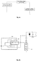
Fig. 1 illustrates a schematic circuit diagram of a solid state pulse modulator according to an embodiment of the present disclosure; -
Fig. 2 illustrates a schematic circuit diagram of a gate protection circuit for an IGBT according to an embodiment of the present disclosure; -
Fig. 3 illustrates a schematic circuit diagram of an oscillation compensation circuit for an IGBT according to an embodiment of the present disclosure; -
Fig. 4a illustrates a schematic structural diagram of an overcurrent protection circuit for an IGBT according to an embodiment of the present disclosure; -
Fig. 4b illustrates a schematic structural diagram of an overcurrent protection circuit for an IGBT according to an embodiment of the present disclosure; -
Fig. 5a illustrates a schematic structural diagram of an overvoltage protection circuit for an IGBT according to an embodiment of the present disclosure; -
Fig. 5b illustrates a schematic structural diagram of an overvoltage protection circuit for an IGBT according to an embodiment of the present disclosure; and -
Fig. 6 illustrates a schematic circuit diagram of a power supply circuit for an IGBT in a solid state pulse modulator based on the MARX generator principle according to an embodiment of the present disclosure. - Other aspects, advantages, and salient features of the present disclosure will become apparent to those skilled in the art according to the following detailed description of the exemplary embodiments of the present disclosure with reference to the drawings.
- In the present disclosure, the terms "comprising" and "including" and their derivatives are meant to be inclusive and not limiting, and the term "or" is inclusive, meaning "and/or."
- In the present specification, the following various embodiments for describing the principles of the present disclosure are merely illustrative, and should not be construed as limiting the scope of the present disclosure in any way. The following description with reference to the accompanying drawings is used to facilitate the complete understanding of exemplary embodiments of the present disclosure defined by the claims and their equivalents, but these details are considered to be merely exemplary. Accordingly, it will be appreciated by those skilled in the art that various changes and modifications may be made to the embodiments described herein without departing from the scope and spirit of the present disclosure. In addition, descriptions of well-known functions and constructions are omitted for clarity and conciseness. In addition, the same reference numerals are used throughout the drawings for similar functions and operations.
-
Fig. 1 illustrates a schematic circuit diagram of a solid state pulse modulator according to an embodiment of the present disclosure. - As shown in
Fig. 1 , the solid state pulse modulator according to this embodiment may comprise a plurality of (for example, 11, depending on pulse voltages required) charging and dischargingmodules 100, and each of the charging and dischargingmodules 100 may comprise acapacitor 1001, anIGBT 1002 anddiode 1003. In each of the charging and dischargingmodules 100, a first terminal of thecapacitor 1001 is connected to a collector of the IGBT, and a second terminal of thecapacitor 1001 is connected to an emitter of the IGBT via thediode 1003. In addition, a gate of the IGBT is connected to a driving circuit (not shown) to be turned on or turned off according to a driving signal from the driving circuit, and accordingly a connection configuration of the capacitors in various charging and dischargingmodules 100 is changed accordingly. The plurality of charging and discharging modules are connected in parallel via diodes. A first charging and dischargingmodule 100 is connected to acapacitor 1004, and a last charging and dischargingmodule 100 is connected in parallel with anotherIGBT 1002 via a diode. - Referring to
Fig. 1 , all IGBTs are turned off in a charging process, so that all capacitors are connected in parallel, and a voltage across each capacitor may be a power supply voltage for charging, for example, 750V, all IGBTs are turned on in a discharging process, so that various capacitors are connected in series via the IGBTs, and thus the voltages across the capacitors may be added to provide a high voltage to the outside. - For IGBTs in such a circuit configuration, a variety of protection measures may be designed.
-
Fig. 2 illustrates a schematic circuit diagram of a gate protection circuit for an IGBT according to an embodiment of the present disclosure. - As shown in
Fig. 2 , the gate protection circuit according to this embodiment comprises avoltage regulator 201 which may supply a stable voltage to an emitter E of the IGBT with respect to the ground for a gate G of the IGBT. For example, the voltage regulator may be avoltage regulation diode 2001. As shown by a dashed box inFig. 2 , a cathode of thevoltage regulation diode 2001 is connected to the emitter E of the IGBT, and an anode of the voltage regulation diode is connected to the ground for the gate G of the IGBT. Additionally, thevoltage regulation diode 2001 is connected in reverse between a positive power supply and the ground for the gate (e.g., via a resistor 2002). Thus, the gate of the IGBT is grounded during a period in which the IGBT needs to be turned off. Therefore, thevoltage regulation diode 2001 is reversely broken down, and thus a constant voltage such as 5V is maintained between the emitter and the gate (at this time, a ground potential). Thus, when the IGBT is turned off, the voltage between the gate and the emitter may be set to a stable negative voltage (for example, -5V). This negative bias can prevent the IGBT from being mis-turned on due to excessive surge current when the IGBT is turned off. - Turn-on resistance of the IGBT decreases when a forward driving voltage increases, to reduce a turn-on loss. However, if the forward driving voltage is too large, the gate may easily be damaged, and therefore it is necessary to appropriately select the forward driving voltage of the
voltage regulation diode 2001, for example, 15V. In addition, after the IGBT is turned on, the driving circuit should provide sufficient voltage and current amplitude to prevent the IGBT from being damaged due to being out of a saturation turn-on region under normal operation and overload conditions. - The voltage between the gate and the emitter of the IGBT is easily disturbed by parasitic parameters of the IGBT and the circuit, when the IGBT is turned off, and therefore the voltage between the gate and the emitter of the IGBT causes the device to be mis-turned on. In order to prevent occurrence of this phenomenon, the gate protection circuit may further comprise a
resistor 3033 connected between the gate G and the emitter E, as shown inFig. 3 . In addition, in practical applications, in order to prevent occurrence of high voltage spikes in the gate driving circuit, the gate protection circuit may further comprise aTVP tube 3034 connected between the gate G and the emitter E, as shown inFig. 3 . As mentioned above, a stable voltage of 15V may be provided across theTVP tube 3034. - In another embodiment, as is known, fast turn-on and turn-off of the IGBT facilitates reducing switch losses. Since the solid state modulator has a very short pulse width (usually only a few us), in the solid state modulator, turn-on and turn-off of the IGBT needs to be performed as fast as possible. Junction capacitance of the gate of the IGBT is usually large, and large driving current is required in order to achieve fast turn-on and turn-off.
- In one example, the driving circuit of the IGBT (shown by the dashed box in
Fig. 3 ) may comprise adriving signal generator 301 and anamplification stage 302. The drivingsignal generator 301 may generate a driving signal (driving pulse) for the IGBT according to a received gate control trigger signal (input at a terminal 4). For example, the drivingsignal generator 301 may comprise a dedicated trigger chip IXDN 604 (reference numerals Fig. 3 indicate respective pins of the IXDN 604). Theamplification stage 302 may amplify the driving signal (e.g., amplify current to achieve large driving current). In one example, theamplification stage 302 may comprise an amplification device such as a triode in a push-pull configuration. On the other hand, the triode may also facilitate the access of an overvoltage protection circuit described below. The driving current of the driving circuit may be large, and internal resistance of the driving circuit may be less than 1 ohm. - Due to the fast triggering speed of the IGBT, distributed inductance and the gate capacitance in the driving circuit form high frequency oscillation. According to an embodiment of the present disclosure, an
oscillation compensation circuit 303 may be provided to at least partially suppress such oscillation. -
Fig. 3 illustrates a schematic circuit diagram of an oscillation compensation circuit for an IGBT according to an embodiment of the present disclosure. - As shown in
Fig. 3 , theoscillation compensation circuit 303 according to this embodiment may comprise anoscillation suppression resistor 3031 connected in series to a gate of the IGBT and anoscillation suppression capacitor 3032 connected in parallel between the gate and an emitter E of the IGBT. A driving signal of the IGBT is input to the gate G of the IGBT via theoscillation suppression resistor 3031, and theoscillation suppression capacitor 3032 is connected between the gate G and the emitter E of the IGBT. Selecting appropriateoscillation suppression resistor 3031 andoscillation suppression capacitor 3032 is advantageous for suppressing oscillation without increasing switching time and switching loss of the IGBT. For example, theoscillation suppression resistor 3031 and theoscillation suppression capacitor 3032 may satisfy the following formula (1):
oscillation suppression resistor 3031, CG is a capacitance value of thesuppression oscillation capacitor 3032, and LG is distributed inductance of the driving circuit for the IGBT. - In one example, junction capacitance of the IGBT used in the solid state modulator is about tens of nF, the distributed inductance in the driving circuit is about tens of nH, and other internal resistance in the driving circuit is about 1 ohm. In this case, for example, RG may be selected as 1 ohm, CG may be selected as 47nF, and at this time a trigger rising edge is about several hundreds of ns.
- In another embodiment, since a load of the solid state modulator is a magnetron, and ignition of the magnetron is unavoidable, an overcurrent problem of the IGBT must be considered. Generally, the overcurrent protection circuit of the IGBT adopts a soft turn-off scheme, since the fast turn-off of the gate voltage may cause the IGBT to be "locked" and cannot be turned off when severe overcurrent of the IGBT happens. The gate voltage requires a reduction process for tens of us to form slow turn-off. However, in a solid state modulator, hard turn-off may be used. This is because in the solid state modulator, an actual turn-on pulse width of the IGBT is very narrow, turn-on operation current of the IGBT is large, and rated current of the selected IGBT is also large. Even in a short-circuit state such as ignition of the magnetron, the short-circuit current has a rise process for more than ten us due to limitation of the distributed inductance in the loop. If the overcurrent fault can be determined in time, turn-off is enabled as soon as possible, and the short-circuit current can be reduced.
- A turn-on voltage drop of the IGBT is very low when the IGBT is normally turned on, and the turn-on voltage drop increases when overcurrent of the IGBT happens. Therefore, the turn-on voltage drop may be detected in the turn-on process, and it may be determined whether overcurrent of the IGBT happens. 4a illustrates a schematic structural diagram of an overcurrent protection circuit for an IGBT according to an embodiment of the present disclosure.
- As shown in
Fig. 4a , the overcurrent protection circuit according to this embodiment may comprise a collectorvoltage detection circuit 401 and anovercurrent trigger circuit 402. - The collector
voltage detection circuit 401 may detect a voltage at a collector of the IGBT during a turn-on phase of the IGBT, and output a signal indicating whether the voltage at the collector exceeds a reference value. According to an embodiment of the present disclosure, the detection of the voltage at the collector by the collectorvoltage detection circuit 401 may be started after a period of time (for example, 1 to 2 us) after the IGBT is turned on, because the voltage drop is relatively large when the IGBT is just turned on. It is easy to cause the collectorvoltage detection circuit 401 to detect a high voltage and thus cause malfunction of the overcurrent protection circuit. - The
overcurrent trigger circuit 402 may output an overcurrent trigger signal to the driving circuit of the IGBT when a signal output by the collector voltage detection circuit indicates that the voltage at the collector exceeds the reference value, so that the driving circuit outputs to the gate of the IGBT a driving signal which causes the IGBT to be turned off. - Thus, the driving circuit may receive two control signals, wherein one of the control signals is a gate control trigger signal which normally controls the IGBT to be turned on/off, and the other of the control signals is the above-described overcurrent trigger signal. In one example, the overcurrent trigger signal may be input to the
driving circuit 404 via an ANDgate 403 along with the gate control trigger signal of the IGBT. For example, as shown inFig. 4b , the overcurrent trigger signal is input to aterminal 2 of an ANDgate 4031, and the gate control trigger signal is input to aterminal 1 of the ANDgate 4031. - The overcurrent trigger circuit may output an overcurrent trigger signal at a low level when the signal output by the collector
voltage detection circuit 401 indicates that the voltage at the collector exceeds the reference value. Due to the action of the AND gate, even if the gate control trigger signal is high (used to drive the IGBT to be turned on), the input of the driving signal is set to be low, thereby turning off the voltage at the gate G. Thus, the current path is disconnected, thereby achieving overcurrent protection. - In one example, the
overcurrent trigger circuit 402 may selectively output a low level signal according to an output of the collectorvoltage detection circuit 401. For example, theovercurrent trigger circuit 402 may comprise a switch device such as afield effect transistor 4021, which has a gate controlled by the output of the collectorvoltage detection circuit 401 to selectively connect theterminal 2 of the ANDgate 4031 to the ground. For example, as shown inFig. 4b , a first terminal of thetransistor 4021 is connected to an input terminal of the ANDgate 403, for example, theterminal 2 of the ANDgate 4031, and a second terminal of thetransistor 4021 is connected to a low level. In response to the signal output by the collectorvoltage detection circuit 401 indicating that the voltage at the collector exceeds a reference value (e.g., a high level applied to the gate of the field effect transistor 4021), thetransistor 4021 is turned on, to turn on a connection between the first terminal and the second terminal, and thus connecting the first terminal (i.e., the input terminal of the AND gate 4031) to the ground. - There are various voltage detection techniques in the art. According to an embodiment of the present disclosure, detection current may be supplied to the collector (via a resistor) to perform voltage detection. For example, the collector
voltage detection circuit 401 may comprise a constantcurrent source 4011. - The constant
current source 4011 may start up (i.e., starting up in synchronization with the turn-on of the IGBT) in response to a driving signal in thedriving circuit 404 which causes the IGBT to be turned on to generate constant detection current. In one example, the constantcurrent source 4011 may comprise a transistor 4011-1. A voltage regulation diode 4011-2 and a resistor 4011-3 are connected between a gate and a drain of the transistor. When the driving signal is high (indicating that the IGBT is turned on), the voltage regulation diode 4011-2 may be reversely broken down and thus a constant voltage is maintained across the voltage regulation diode 4011-2. This constant voltage produces constant emitter current via the resistor 4011-3, and thus substantially constant current may be output by the collector for use as the detection current. Of course, the configuration of the constant current source is not limited thereto. - As described above, the detection current needs to be supplied to the collector after a period of time after the IGBT is turned on to avoid malfunction, and therefore, the collector
voltage detection circuit 401 according to this embodiment may further comprise adelay mechanism 4012. Thedelay mechanism 4012 causes the constant current generated by the constantcurrent source 4011 to be supplied to the collector C of the IGBT when a predetermined time elapses after the constant current source starts up. - In one example, the
delay mechanism 4012 may comprise a capacitor, such as a capacitor 4012-1 shown inFig. 4b . For example, an output terminal of the constantcurrent source 4011 is connected to a first terminal of the capacitor on the one hand and to the collector C of the IGBT via adetection resistor 405 on the other hand. A second terminal of the capacitor 4012-1 may be connected to the ground potential. There is a unidirectional conduction device such as adiode 406 between the constantcurrent source 4011 and the collector C, so that the capacitor can only be charged by the current from the constant current source (thereby, for example, preventing the collector C from charging the capacitor 4012-1 when there is a high voltage at the collector C). - It is assumed that there is no charge in the capacitor 4012-1 in an initial state of the circuit, and therefore a voltage at the first terminal thereof (a voltage at a node P1) is approximately zero. At the moment when the IGBT is turned on, the constant current source starts up, and thus constant detection current is generated. Since the voltage at P1 is low at this time (the
diode 406 is reversely biased), the detection current mainly charges the capacitor 4012-1. In addition, the voltage which is low at the node P1 does not cause thevoltage regulation diode 407 to be reversely broken down, thus the gate of thetransistor 4021 is connected to the ground via aresistor 408, and therefore thetransistor 4021 is turned off, so that the input at theterminal 2 of the ANDgate 4031 is high. In this case, the generation of the driving signal depends on the gate control trigger signal. - As the detection current charges the capacitor 4012-1, the voltage at P1 gradually increases. In a case of normal operation, when a period of time elapses after the IGBT is turned on, the voltage at the collector decreases (close to the voltage at the emitter). When the voltage at P1 increases to be above the voltage at the collector, the detection current may flow into the collector C. That is, the detection current is delayed by the time required for the voltage at P1 to increase to be above the voltage at the collector. At this time, the voltage at P1 is approximately the voltage at the collector + the detection current *R1, where R1 represents a resistance value of the
resistor 405. A current value of the detection current, a resistance value of theresistor 405, and parameters of thevoltage regulation diode 407 may be selected so that thevoltage regulation diode 407 is not reversely broken down at this time, and thus the input at theterminal 2 of the ANDgate 4031 is maintained at a high level. - In a case of overcurrent, the voltage at the collector may increase. Due to the presence of the
unidirectional conduction device 406, the detection current may further charge the capacitor 4012-1 and thus the voltage at P1 increases. Finally, the voltage at P1 may cause thevoltage regulation diode 407 to be reversely broken down and thus a constant voltage is maintained across thevoltage regulation diode 407. The presence of this voltage may cause thetransistor 4021 to be turned on, and thus pull down the input at theterminal 2 of the ANDgate 4031 to the ground potential. In response to this low input, the driving circuit may cause the IGBT to be turned off. - In this example, the collector
voltage detection circuit 401 converts a high voltage and a low voltage at the collector to a high level signal and a low level signal by thevoltage regulation diode 407 and theresistor 408 connected between the first terminal of the capacitor 4012-1 and the ground potential. The high level signal and the low level signal are output at a connection node between thevoltage regulation diode 407 and theresistor 408 to control theovercurrent trigger circuit 402. However, the present disclosure is not limited thereto. There are various techniques in the art to convert the high voltage and low voltage at P1 into corresponding high and low level control signals, respectively. - In another embodiment, the IGBT in the solid state modulator needs to be turned off quickly, and a high surge spike voltage UCE may be generated between the collector C and the emitter E of the IGBT due to the action of stray inductance and load inductance in the circuit. In addition, the overvoltage resistance of the IGBT is poor, which may cause the IGBT to be broken down. Therefore, overvoltage protection of the IGBT is also very important. A method of reducing the voltage UCE between the collector and the emitter of the IGBT may be to increase resistance RG of the gate. However, the increase of RG may slow down the turn-on/off speed of the IGBT, thereby increasing the turn-on/off loss. Accordingly, this method is not ideal.
-
Fig. 5a illustrates an overvoltage protection circuit for an IGBT according to an embodiment of the present disclosure. - As shown in
Fig. 5a , the overvoltage protection circuit according to this embodiment may comprise a collectorvoltage detection circuit 501 and anovervoltage trigger circuit 502. - The collector
voltage detection circuit 501 may detect a voltage at a collector of the IGBT during a turn-off phase of the IGBT, and output a signal indicating whether the voltage at the collector exceeds a reference value. The reference value may be, for example, 750V depending on actual needs. For example, the collectorvoltage detection circuit 501 may comprise one or more TVP tubes connected in series, as shown inFig. 5b . A number of the TVP tubes may be determined according to the above reference value, for example, the number of the TVP tubes is 3 in a case that the reference value is 750V. In this case, during the turn-off phase of the IGBT, when the voltage at the collector is too high (surge voltage), the collectorvoltage detection circuit 501 may output a high level signal. - The
overvoltage trigger circuit 502 may output an overvoltage trigger signal to adriving circuit 503 of the IGBT when the signal output by the collectorvoltage detection circuit 501 indicates that the voltage at the collector exceeds the reference value, so that the drivingcircuit 503 outputs to a gate of the IGBT a driving signal which causes the IGBT to be turned on. - In one example, an output terminal of the
overvoltage trigger circuit 502 may be connected to a control terminal of a high side transistor (e.g., 5001 shown inFig. 5b ) of a driving current amplifier circuit in push-pull configuration in thedriving circuit 503 of the IGBT. In this case, in a case of determining the overvoltage (that is, the output signal of the collectorvoltage detection circuit 501 indicates that the voltage at the collector exceeds the reference value), theovervoltage trigger circuit 502 may output a high level signal to cause the high side transistor to be turned on, and thus output to the gate of the IGBT a driving signal for driving the IGBT to be turned on. As shown inFig. 5b , when the collectorvoltage detection circuit 501 indicates that the voltage at the collector is too high using a high level signal, theovervoltage trigger circuit 502 may simply connect an output node of the collector voltage detection circuit 501 (via a resistor) to a gate of the high side transistor. - Thus, when the voltage at the collector exceeds the reference value, the gate of the IGBT may be turned on to release a certain amount of electrical energy to form appropriate slow turn-off. For example, as shown in
Fig. 5b , when the voltage at the collector exceeds a voltage of the TVP tube, current flows through the TVP tube, is amplified by the triode and is then applied to the gate of the IGBT, the IGBT is turned on to release the electrical energy, and then the voltage of the IGBT decreases. When the voltage at the collector decreases to be below a voltage drop of the TVP tube, the gate is turned off. In this way, adaptive slow turn-off is formed to achieve overvoltage protection. - As a backup, an additional overvoltage protection branch may also be provided. The overvoltage protection branch may output a signal which causes the IGBT to be turned on to the gate of the IGBT when the signal output by the collector voltage detection circuit indicates that the voltage at the collector exceeds the reference value. As shown in
Fig. 5b , when the collectorvoltage detection circuit 501 indicates that the voltage at the collector is too high using a high level signal, the additional overvoltage protection branch may simply connect the output node of the collectorvoltage detection circuit 501 to the gate of the IGBT (via a resistor). - In another embodiment, because the MARX discharge loop is employed, various IGBT modules are floated differently at different high voltages, and both triggering and power supply for the triggering need to be isolated. For example, the triggering may be transmitted through an optical fiber, and the power supply for the triggering may be realized using a method for coupling high-frequency current with a current transformer, may be transmitted through a high-voltage-resistant wire, wherein a primary transformer may be implemented using a 1-turn transformer.
-
Fig. 6 illustrates a schematic circuit diagram of a power supply circuit for an IGBT in a solid state pulse modulator based on MARX generator principle according to an embodiment of the present disclosure. - As shown in
Fig. 6 , the power supply circuit according to this embodiment may comprise amutual inductance coil 601, a conductive wire, abridge rectifier 602, and avoltage regulation diode 603. The conductive wire is coupled to the mutual inductance coil and passes through the mutual inductance coil for transmitting alternating current and thus generating an alternating current signal in the mutual inductance coil. Thebridge rectifier 602 converts the alternating current signal into a direct current signal to power a driving circuit. Apositive output terminal 3 of thebridge rectifier 602 provides a power supply voltage and anegative output terminal 4 of thebridge rectifier 602 is connected to the ground for a gate of the IGBT. Thevoltage regulation diode 603 is connected between the positive output terminal and the negative output terminal of the rectifier. - In another embodiment, the present disclosure further provides a solid state pulse modulator based on the MARX generator principle, comprising one or more of the gate protection circuit, the oscillation compensation circuit, the overcurrent protection circuit, the overvoltage protection circuit, and the power supply circuit as described above.
- In the solid state pulse modulator based on the MARX generator principle, the present disclosure can ensure the safety and reliability of the IGBT.
- The above described methods, apparatus, units and/or modules in accordance with various embodiments of the present disclosure may be implemented by execution of software comprising computer instructions by a computational electronic device. The system may comprise storage devices to implement the various storages described above. The computational electronic device may comprise a general purpose processor, a digital signal processor, a dedicated processor, a reconfigurable processor, etc., which can execute computer instructions, but is not limited thereto. Execution of such instructions causes the electronic device to be configured to perform the operations described above in accordance with the present disclosure. Each of the above devices and/or modules may be implemented in one electronic device or in different electronic devices. The software can be stored in a computer readable storage medium. The computer readable storage medium stores one or more programs (software modules), the one or more programs including instructions that, when executed by one or more processors in an electronic device, cause the electronic device to execute methods of the present disclosure.
- The software may be stored in the form of volatile memory or non-volatile storage (e.g., a storage device like a ROM), whether erasable or rewritable, or stored in the form of a memory (e.g., RAM, memory chip, device or integrated circuit) is either stored on an optically readable medium or a magnetically readable medium (e.g., CD, DVD, magnetic disk or magnetic tape, etc.). It should be appreciated that the storage device and the storage medium are embodiments of a machine-readable storage device adapted to store one or more programs, the one or more programs comprising instructions that, when executed, implement an embodiment of the present disclosure. The embodiment provides a program and a machine readable storage device storing such a program, the program comprising code for implementing the apparatus or method of any of the claims of the present disclosure. Moreover, these programs can be transferred via any medium, such as a communication signal carried via a wired connection or a wireless connection, and various embodiments suitably include such programs.
- Methods, apparatus, units, and/or modules in accordance with various embodiments of the present disclosure may be implemented by, for example, a field programmable gate array (FPGA), a programmable logic array (PLA), a system on a chip, a system on a substrate, a system on a package, an application specific integrated circuit (ASIC), or in hardware or firmware, such as in any other reasonable manner for integrating or encapsulating the circuit, or in a suitable combination of three implementations of software, hardware, and firmware. The system may comprise a storage device to implement the storage described above. When implemented in these manners, the software, hardware, and/or firmware used is programmed or designed to perform the respective methods, steps and/or functions described above in accordance with the present disclosure. One skilled in the art can appropriately implement one or more of these systems and modules, or a part of some parts of them, using different implementations described above, according to actual needs. These implementations fall within the scope of protection of the present disclosure.
- While the present disclosure has been shown and described with respect to the specific embodiments of the embodiments of the present invention, it may be understood by those skilled in the art that various changes in form and detail are made to the present disclosure without departing from the spirit and scope of the disclosure as defined by the appended claims and their equivalents. Therefore, the scope of the present disclosure should not be limited to the above-described embodiments, but should be determined not only by the appended claims but also by the equivalents of the appended claims.
Claims (15)
- A solid state pulse modulator based on the MARX generator principle, comprising a gate protection circuit for an Insulated Gate Bipolar Transistor (IGBT), the IGBT being used as a switch device in a solid state pulse modulator based on the MARX generator principle, the gate protection circuit comprising:
a voltage regulator configured to supply a stable voltage to an emitter of the IGBT with respect to the ground for a gate of the IGBT. - The solid state pulse modulator according to claim 1, wherein the voltage regulator is a voltage regulation diode having a cathode connected to an emitter of the IGBT, and an anode connected to the ground for the gate of the IGBT.
- The solid state pulse modulator according to claim 1, further comprising an oscillation compensation circuit for the IGBT, the oscillation compensation circuit comprising:an oscillation suppression resistor RG, wherein a driving signal of the IGBT is input to a gate of the IGBT via the oscillation suppression resistor; andan oscillation suppression capacitor CG connected between the gate and an emitter of the IGBT.
- The solid state pulse modulator according to claim 3, wherein the oscillation suppression resistor RG and the oscillation suppression capacitor CG satisfy the following formula:

- The solid state pulse modulator according to claim 1, further comprising an overcurrent protection circuit for the IGBT, the overcurrent protection circuit comprising:a collector voltage detection circuit configured to detect a voltage at a collector of the IGBT during a turn-on phase of the IGBT, and output a signal indicating whether the voltage at the collector exceeds a reference value; andan overcurrent trigger circuit configured to output an overcurrent trigger signal to the driving circuit of the IGBT when the signal output by the collector voltage detection circuit indicates that the voltage at the collector exceeds the reference value, so that the driving circuit outputs to the gate of the IGBT a driving signal which causes the IGBT to be turned off.
- The solid state pulse modulator according to claim 5, wherein the overcurrent trigger signal is input to the driving circuit through an AND gate together with a gate control trigger signal of the IGBT, and
wherein, when the signal output by the collector voltage detection circuit indicates that the voltage at the collector exceeds the reference value, the overcurrent trigger circuit outputs the overcurrent trigger signal at a low level. - The solid state pulse modulator according to claim 6, wherein the overcurrent trigger circuit comprises a transistor having a first terminal connected to an input terminal of the AND gate, and a second terminal connected to a low level, and
wherein, in response to the signal output by the collector voltage detection circuit indicating that the voltage at the collector exceeds the reference value, the transistor is turned on to turn on a connection between the first terminal and the second terminal. - The solid state pulse modulator according to claim 5, wherein the collector voltage detection circuit is configured to detect the voltage at the collector for a predetermined time after a time at which the IGBT starts to be turned on.
- The solid state pulse modulator according to claim 8, wherein the collector voltage detection circuit comprises:a constant current source configured to start up in response to the driving signal in the driving circuit which causes the IGBT to be turned on, to generate constant detection current; anda delay mechanism configured to cause the constant detection current generated by the constant current source to be supplied to the collector of the IGBT when a predetermined time elapses after the constant current source starts up.
- The solid state pulse modulator according to claim 9, wherein the delay mechanism comprises a capacitor,
wherein an output terminal of the constant current source is connected on the one hand to a first terminal of the capacitor and on the other hand to the collector of the IGBT via a detection resistor, wherein a second terminal of the capacitor is connected to a ground potential, and
wherein there is a unidirectional conduction device between the constant current source and the collector, so that the capacitor can only be charged by the current from the constant current source. - The solid state pulse modulator according to claim 10, wherein the collector voltage detection circuit further comprises: a voltage regulation diode and a resistor connected between the first terminal of the capacitor and the ground potential, and
wherein a connection node between the voltage regulation diode and the resistor is used as an output node of the collector voltage detection circuit. - The solid state pulse modulator according to claim 1, further comprising an overvoltage protection circuit for the IGBT, the overvoltage protection circuit comprising:a collector voltage detection circuit configured to detect a voltage at a collector of the IGBT during a turn-off phase of the IGBT, and output a signal indicating whether the voltage at the collector exceeds a reference value; andan overvoltage trigger circuit configured to output an overvoltage trigger signal to a driving circuit of the IGBT when the signal output by the collector voltage detection circuit indicates that the voltage at the collector exceeds the reference value, so that the driving circuit outputs to a gate of the IGBT a driving signal which causes the IGBT to be turned on.
- The solid state pulse modulator according to claim 12, further comprising an additional overvoltage protection branch configured to output to the gate of the IGBT a signal for causing the IGBT to be turned on when the signal output by the collector voltage detection circuit indicates that the voltage at the collector exceeds the reference value.
- The solid state pulse modulator according to claim 1, further comprising a power supply circuit for a driving circuit of the IGBT, comprising:a mutual inductance coil;a conductive wire coupled to the mutual inductance coil, and configured to transmit alternating current and thus generate an alternating current signal in the mutual inductance coil;a rectifier configured to convert the alternating current signal into a direct current signal to supply power to the driving circuit, wherein a positive output terminal of the rectifier provides a power supply voltage, and a negative output terminal of the rectifier is connected to a ground for a gate of the IGBT; anda voltage regulation diode connected between the positive output terminal and the negative output terminal of the rectifier.
- The solid state pulse modulator according to claim 14, wherein the conductive wire passes through the mutual inductance coil.
Applications Claiming Priority (1)
| Application Number | Priority Date | Filing Date | Title |
|---|---|---|---|
| CN201710858572.7A CN107835002B (en) | 2017-09-20 | 2017-09-20 | Protection circuit, oscillation compensation circuit and power supply circuit in solid-state pulse modulator |
Publications (3)
| Publication Number | Publication Date |
|---|---|
| EP3461006A2 true EP3461006A2 (en) | 2019-03-27 |
| EP3461006A3 EP3461006A3 (en) | 2019-06-26 |
| EP3461006B1 EP3461006B1 (en) | 2022-05-04 |
Family
ID=61643960
Family Applications (1)
| Application Number | Title | Priority Date | Filing Date |
|---|---|---|---|
| EP18190829.4A Active EP3461006B1 (en) | 2017-09-20 | 2018-08-24 | Protection circuit, oscillation compensation circuit and power supply circuit in solid state pulse modulator |
Country Status (6)
| Country | Link |
|---|---|
| US (1) | US11152932B2 (en) |
| EP (1) | EP3461006B1 (en) |
| JP (1) | JP6691180B2 (en) |
| KR (1) | KR102091693B1 (en) |
| CN (1) | CN107835002B (en) |
| AU (1) | AU2018220119B2 (en) |
Families Citing this family (13)
| Publication number | Priority date | Publication date | Assignee | Title |
|---|---|---|---|---|
| DE102018221518A1 (en) * | 2018-12-12 | 2020-06-18 | Siemens Healthcare Gmbh | High-voltage generator for providing a high-voltage pulse |
| CN109581179A (en) * | 2018-12-24 | 2019-04-05 | 天津城建大学 | A kind of insulated gate bipolar transistor junction temperature measurement method |
| JP7253739B2 (en) * | 2019-08-23 | 2023-04-07 | 株式会社デンソー | marx circuit |
| CN110597095A (en) * | 2019-09-24 | 2019-12-20 | 广州华工科技开发有限公司 | Controller based on IGBT |
| CN110726867B (en) * | 2019-11-14 | 2024-08-30 | 南方电网科学研究院有限责任公司 | A fast response detection circuit for tube voltage drop suitable for bridge circuit |
| CN110932564A (en) * | 2019-12-18 | 2020-03-27 | 广州邦讯信息系统有限公司 | A low-noise self-excited push-pull converter |
| CN112731548B (en) * | 2021-01-18 | 2023-08-29 | 厦门汉印电子技术有限公司 | Photoelectric pair control method, photoelectric pair control device, photoelectric pair control equipment and readable storage medium |
| CN113030787A (en) * | 2021-03-15 | 2021-06-25 | 南京朗驰瑞泰电子信息技术有限公司 | Online detection method for high-voltage solid rigid tube modulator |
| CN114337198B (en) * | 2022-02-10 | 2025-10-31 | 西安科湃电气有限公司 | High-power multichannel multi-level IGBT driving circuit with protection function |
| CN115468632B (en) * | 2022-10-19 | 2023-10-20 | 佛山市汉立电子科技有限公司 | Liquid shortage detection device and method and atomizer |
| CN115967374B (en) * | 2022-12-19 | 2023-09-19 | 重庆大学 | A high-voltage pulse generating device based on all-solid-state switch hybrid connection |
| CN119395363B (en) * | 2024-11-14 | 2026-07-24 | 华北电力科学研究院有限责任公司 | Method and apparatus for determining the peak value of Class II short-circuit transient current in IGBT devices |
| CN121439656A (en) * | 2025-10-29 | 2026-01-30 | 东方晶源微电子科技(北京)股份有限公司 | Electron beam scanning equipment and its voltage regulation circuit |
Family Cites Families (45)
| Publication number | Priority date | Publication date | Assignee | Title |
|---|---|---|---|---|
| JPH027714A (en) * | 1988-06-27 | 1990-01-11 | Hitachi Ltd | Protection device for elements during abnormal current |
| JPH0479758A (en) * | 1990-07-19 | 1992-03-13 | Fuji Electric Co Ltd | Driving circuit of current sensing igbt |
| DE59010931D1 (en) * | 1990-12-08 | 2003-03-06 | Abb Schweiz Ag | Switching arrangement for an HF GTO |
| JP3032745B2 (en) * | 1992-09-04 | 2000-04-17 | 三菱電機株式会社 | Insulated gate type semiconductor device |
| JP3139223B2 (en) * | 1992-11-26 | 2001-02-26 | 富士電機株式会社 | Semiconductor device and manufacturing method thereof |
| JPH07111446A (en) * | 1993-10-14 | 1995-04-25 | Hitachi Ltd | Gate drive device for voltage driven semiconductor device |
| JP3373704B2 (en) * | 1995-08-25 | 2003-02-04 | 三菱電機株式会社 | Insulated gate transistor drive circuit |
| JP3560274B2 (en) * | 1997-09-19 | 2004-09-02 | オリジン電気株式会社 | Method and circuit for driving electric field control type semiconductor device |
| JP2000152617A (en) * | 1998-11-10 | 2000-05-30 | Sony Corp | Switching power supply circuit |
| JP4449190B2 (en) * | 1999-08-10 | 2010-04-14 | 富士電機システムズ株式会社 | Voltage-driven semiconductor device gate drive device |
| JP2002208847A (en) * | 2001-01-12 | 2002-07-26 | Fuji Electric Co Ltd | Gate drive circuit for power semiconductor device |
| JP3791393B2 (en) | 2001-10-23 | 2006-06-28 | 富士電機デバイステクノロジー株式会社 | Inverter circuit |
| JP2005032736A (en) * | 2002-06-10 | 2005-02-03 | Fuji Electric Holdings Co Ltd | Semiconductor device and manufacturing method thereof |
| KR100539401B1 (en) | 2003-07-25 | 2005-12-27 | 재단법인서울대학교산학협력재단 | Protection circuit of insulated gate type power device for short-circuit withstanding |
| JP2005287182A (en) * | 2004-03-30 | 2005-10-13 | Yaskawa Electric Corp | Gate drive circuit for voltage driven semiconductor device |
| FR2874767B1 (en) * | 2004-08-27 | 2006-10-20 | Schneider Toshiba Inverter | DEVICE FOR CONTROLLING A POWER TRANSISTOR |
| US7855904B2 (en) * | 2005-03-17 | 2010-12-21 | Los Alamos National Security, Llc | Apparatus for producing voltage and current pulses |
| JP4727360B2 (en) * | 2005-09-20 | 2011-07-20 | 東芝三菱電機産業システム株式会社 | Gate circuit of insulated gate semiconductor device |
| JP4432953B2 (en) * | 2006-09-27 | 2010-03-17 | 株式会社日立製作所 | Semiconductor power converter |
| JP2008154371A (en) * | 2006-12-18 | 2008-07-03 | Toyota Motor Corp | VEHICLE DRIVE DEVICE, VEHICLE DRIVE DEVICE CONTROL METHOD, PROGRAM FOR CAUSING COMPUTER TO EXECUTE VEHICLE DRIVE DEVICE CONTROL METHOD, AND RECORDING MEDIUM CONTAINING THE PROGRAM readable |
| US7508096B1 (en) * | 2007-09-20 | 2009-03-24 | General Electric Company | Switching circuit apparatus having a series conduction path for servicing a load and switching method |
| US8770496B2 (en) * | 2008-03-10 | 2014-07-08 | Finishing Brands Holdings Inc. | Circuit for displaying the relative voltage at the output electrode of an electrostatically aided coating material atomizer |
| JP2009253484A (en) * | 2008-04-03 | 2009-10-29 | Fuji Electric Systems Co Ltd | Power conversion device |
| EP2320544B1 (en) | 2008-08-21 | 2019-02-20 | Mitsubishi Electric Corporation | Driving circuit for power semiconductor element |
| JP5394975B2 (en) * | 2010-04-21 | 2014-01-22 | 住友重機械工業株式会社 | Switching transistor control circuit and power converter using the same |
| DE102010038731B3 (en) * | 2010-07-30 | 2011-12-08 | Semikron Elektronik Gmbh & Co. Kg | Submodule and power semiconductor module |
| JP5556584B2 (en) | 2010-10-26 | 2014-07-23 | トヨタ自動車株式会社 | Inverter drive |
| US8400739B2 (en) * | 2011-02-28 | 2013-03-19 | General Electric Company | System and method for operating inverters |
| CN103036415B (en) * | 2011-09-29 | 2015-07-08 | 台达电子企业管理(上海)有限公司 | Power semiconductor switch series circuit and control method thereof |
| CN102545687A (en) * | 2011-12-31 | 2012-07-04 | 同方威视技术股份有限公司 | Device and method for outputting voltage alternative pulses |
| US9531441B2 (en) * | 2012-02-21 | 2016-12-27 | Lg Innotek Co., Ltd. | Wireless power receiver and method of managing power thereof |
| JP5500192B2 (en) * | 2012-03-16 | 2014-05-21 | 株式会社デンソー | Switching element drive circuit |
| RU2624452C2 (en) * | 2012-04-12 | 2017-07-04 | Филипс Лайтинг Холдинг Б.В. | Interface digital communication circuit for wired pair with individually adjustable transition borders |
| CN103427809B (en) * | 2012-05-21 | 2016-04-20 | 永济新时速电机电器有限责任公司 | The protective circuit of insulated gate bipolar transistor |
| JP6015615B2 (en) | 2013-10-01 | 2016-10-26 | 三菱電機株式会社 | Semiconductor device |
| JP6156073B2 (en) | 2013-11-08 | 2017-07-05 | 株式会社明電舎 | Semiconductor switching element protection circuit and power conversion device |
| JP2015115976A (en) * | 2013-12-09 | 2015-06-22 | 東芝三菱電機産業システム株式会社 | Gate drive circuit |
| KR102155031B1 (en) * | 2013-12-30 | 2020-09-11 | 삼성전자주식회사 | Power supply and gate driver therein |
| CN104378097B (en) * | 2014-09-29 | 2018-06-12 | 株洲变流技术国家工程研究中心有限公司 | The drive system and method for a kind of insulated gate bipolar transistor |
| JP6252561B2 (en) | 2015-07-28 | 2017-12-27 | トヨタ自動車株式会社 | electric circuit |
| KR102276588B1 (en) * | 2015-08-25 | 2021-07-13 | 한국전자기술연구원 | Igbt driving circuit |
| US9787303B2 (en) * | 2015-12-03 | 2017-10-10 | General Electric Company | Driver circuit and switch driving method |
| CN205847212U (en) * | 2016-07-08 | 2016-12-28 | 上海众联能创新能源科技股份有限公司 | A kind of IGBT drive circuit of high reliability |
| CN207475519U (en) * | 2017-09-20 | 2018-06-08 | 同方威视技术股份有限公司 | Protection circuit, oscillation compensation circuit and power supply circuit in solid state pulse modulator |
| CN110768649B (en) * | 2018-07-26 | 2023-03-24 | 台达电子工业股份有限公司 | Gate circuit and gate drive circuit of power semiconductor switch |
-
2017
- 2017-09-20 CN CN201710858572.7A patent/CN107835002B/en active Active
-
2018
- 2018-08-13 JP JP2018152248A patent/JP6691180B2/en active Active
- 2018-08-16 KR KR1020180095406A patent/KR102091693B1/en active Active
- 2018-08-23 US US16/110,355 patent/US11152932B2/en active Active
- 2018-08-24 AU AU2018220119A patent/AU2018220119B2/en active Active
- 2018-08-24 EP EP18190829.4A patent/EP3461006B1/en active Active
Non-Patent Citations (1)
| Title |
|---|
| None |
Also Published As
| Publication number | Publication date |
|---|---|
| CN107835002B (en) | 2024-03-12 |
| US11152932B2 (en) | 2021-10-19 |
| CN107835002A (en) | 2018-03-23 |
| EP3461006A3 (en) | 2019-06-26 |
| KR102091693B1 (en) | 2020-03-23 |
| EP3461006B1 (en) | 2022-05-04 |
| KR20190032998A (en) | 2019-03-28 |
| JP2019058056A (en) | 2019-04-11 |
| AU2018220119B2 (en) | 2020-07-23 |
| AU2018220119A1 (en) | 2019-04-04 |
| US20190089344A1 (en) | 2019-03-21 |
| JP6691180B2 (en) | 2020-04-28 |
Similar Documents
| Publication | Publication Date | Title |
|---|---|---|
| US11152932B2 (en) | Protection circuit, oscillation compensation circuit and power supply circuit in solid state pulse modulator | |
| CN115549456B (en) | Protection Circuit and Control Method of Flyback Converter | |
| US9698654B2 (en) | Soft shutdown for isolated drivers | |
| CN108809059B (en) | Driving device for semiconductor element | |
| US10236677B2 (en) | Semiconductor device | |
| US9035681B2 (en) | Switch controller, switch control method, and power supply device comprising the switch controller | |
| JP5747445B2 (en) | Gate drive device | |
| CN112838746A (en) | Gate Driver with Integrated Miller Clamp | |
| US20100103705A1 (en) | Short circuit protection circuit for a pulse width modulation (pwm) unit | |
| US7368972B2 (en) | Power transistor control device | |
| TWI661675B (en) | Driving circuit for power semiconductor switch | |
| US9692406B2 (en) | Power device drive circuit | |
| EP4156484B1 (en) | Drive circuit having energy recovery function, and switch power supply | |
| CN112640279B (en) | Overcurrent protection circuit and switch circuit | |
| US9653998B2 (en) | Boost converter and power controling method thereof | |
| CN111740387A (en) | Short circuit protection circuit and motor controller | |
| CN112332821B (en) | A MOSFET passive isolation anti-through fast-off driving circuit | |
| US20260088710A1 (en) | Control method for inverter circuit, power conversion apparatus, and energy storage device | |
| CN113193861B (en) | A circuit and control method for preventing semiconductor switch device from being turned on by mistake | |
| CN207475519U (en) | Protection circuit, oscillation compensation circuit and power supply circuit in solid state pulse modulator | |
| CN120223032A (en) | A gallium nitride driving circuit | |
| CN220254351U (en) | A driving circuit, power circuit, circuit board and switching power supply | |
| CN120185393A (en) | Isolation circuit and energy recovery circuit and method thereof | |
| CN109150139B (en) | Narrow pulse width pulse output circuit | |
| CN117674578A (en) | Power-on slow start circuit, chip and laser radar |
Legal Events
| Date | Code | Title | Description |
|---|---|---|---|
| PUAI | Public reference made under article 153(3) epc to a published international application that has entered the european phase |
Free format text: ORIGINAL CODE: 0009012 |
|
| STAA | Information on the status of an ep patent application or granted ep patent |
Free format text: STATUS: THE APPLICATION HAS BEEN PUBLISHED |
|
| AK | Designated contracting states |
Kind code of ref document: A2 Designated state(s): AL AT BE BG CH CY CZ DE DK EE ES FI FR GB GR HR HU IE IS IT LI LT LU LV MC MK MT NL NO PL PT RO RS SE SI SK SM TR |
|
| AX | Request for extension of the european patent |
Extension state: BA ME |
|
| PUAL | Search report despatched |
Free format text: ORIGINAL CODE: 0009013 |
|
| AK | Designated contracting states |
Kind code of ref document: A3 Designated state(s): AL AT BE BG CH CY CZ DE DK EE ES FI FR GB GR HR HU IE IS IT LI LT LU LV MC MK MT NL NO PL PT RO RS SE SI SK SM TR |
|
| AX | Request for extension of the european patent |
Extension state: BA ME |
|
| RIC1 | Information provided on ipc code assigned before grant |
Ipc: H03K 17/0812 20060101ALI20190523BHEP Ipc: H03K 17/06 20060101AFI20190523BHEP Ipc: H03K 3/57 20060101ALI20190523BHEP |
|
| STAA | Information on the status of an ep patent application or granted ep patent |
Free format text: STATUS: REQUEST FOR EXAMINATION WAS MADE |
|
| 17P | Request for examination filed |
Effective date: 20191223 |
|
| STAA | Information on the status of an ep patent application or granted ep patent |
Free format text: STATUS: EXAMINATION IS IN PROGRESS |
|
| 17Q | First examination report despatched |
Effective date: 20200902 |
|
| GRAP | Despatch of communication of intention to grant a patent |
Free format text: ORIGINAL CODE: EPIDOSNIGR1 |
|
| STAA | Information on the status of an ep patent application or granted ep patent |
Free format text: STATUS: GRANT OF PATENT IS INTENDED |
|
| INTG | Intention to grant announced |
Effective date: 20211117 |
|
| GRAS | Grant fee paid |
Free format text: ORIGINAL CODE: EPIDOSNIGR3 |
|
| GRAA | (expected) grant |
Free format text: ORIGINAL CODE: 0009210 |
|
| STAA | Information on the status of an ep patent application or granted ep patent |
Free format text: STATUS: THE PATENT HAS BEEN GRANTED |
|
| AK | Designated contracting states |
Kind code of ref document: B1 Designated state(s): AL AT BE BG CH CY CZ DE DK EE ES FI FR GB GR HR HU IE IS IT LI LT LU LV MC MK MT NL NO PL PT RO RS SE SI SK SM TR |
|
| REG | Reference to a national code |
Ref country code: GB Ref legal event code: FG4D |
|
| REG | Reference to a national code |
Ref country code: CH Ref legal event code: EP |
|
| REG | Reference to a national code |
Ref country code: AT Ref legal event code: REF Ref document number: 1490220 Country of ref document: AT Kind code of ref document: T Effective date: 20220515 |
|
| REG | Reference to a national code |
Ref country code: DE Ref legal event code: R096 Ref document number: 602018034819 Country of ref document: DE |
|
| REG | Reference to a national code |
Ref country code: IE Ref legal event code: FG4D |
|
| REG | Reference to a national code |
Ref country code: SE Ref legal event code: TRGR |
|
| REG | Reference to a national code |
Ref country code: LT Ref legal event code: MG9D |
|
| REG | Reference to a national code |
Ref country code: NL Ref legal event code: MP Effective date: 20220504 |
|
| REG | Reference to a national code |
Ref country code: AT Ref legal event code: MK05 Ref document number: 1490220 Country of ref document: AT Kind code of ref document: T Effective date: 20220504 |
|
| PG25 | Lapsed in a contracting state [announced via postgrant information from national office to epo] |
Ref country code: PT Free format text: LAPSE BECAUSE OF FAILURE TO SUBMIT A TRANSLATION OF THE DESCRIPTION OR TO PAY THE FEE WITHIN THE PRESCRIBED TIME-LIMIT Effective date: 20220905 Ref country code: NO Free format text: LAPSE BECAUSE OF FAILURE TO SUBMIT A TRANSLATION OF THE DESCRIPTION OR TO PAY THE FEE WITHIN THE PRESCRIBED TIME-LIMIT Effective date: 20220804 Ref country code: NL Free format text: LAPSE BECAUSE OF FAILURE TO SUBMIT A TRANSLATION OF THE DESCRIPTION OR TO PAY THE FEE WITHIN THE PRESCRIBED TIME-LIMIT Effective date: 20220504 Ref country code: LT Free format text: LAPSE BECAUSE OF FAILURE TO SUBMIT A TRANSLATION OF THE DESCRIPTION OR TO PAY THE FEE WITHIN THE PRESCRIBED TIME-LIMIT Effective date: 20220504 Ref country code: HR Free format text: LAPSE BECAUSE OF FAILURE TO SUBMIT A TRANSLATION OF THE DESCRIPTION OR TO PAY THE FEE WITHIN THE PRESCRIBED TIME-LIMIT Effective date: 20220504 Ref country code: GR Free format text: LAPSE BECAUSE OF FAILURE TO SUBMIT A TRANSLATION OF THE DESCRIPTION OR TO PAY THE FEE WITHIN THE PRESCRIBED TIME-LIMIT Effective date: 20220805 Ref country code: FI Free format text: LAPSE BECAUSE OF FAILURE TO SUBMIT A TRANSLATION OF THE DESCRIPTION OR TO PAY THE FEE WITHIN THE PRESCRIBED TIME-LIMIT Effective date: 20220504 Ref country code: ES Free format text: LAPSE BECAUSE OF FAILURE TO SUBMIT A TRANSLATION OF THE DESCRIPTION OR TO PAY THE FEE WITHIN THE PRESCRIBED TIME-LIMIT Effective date: 20220504 Ref country code: BG Free format text: LAPSE BECAUSE OF FAILURE TO SUBMIT A TRANSLATION OF THE DESCRIPTION OR TO PAY THE FEE WITHIN THE PRESCRIBED TIME-LIMIT Effective date: 20220804 Ref country code: AT Free format text: LAPSE BECAUSE OF FAILURE TO SUBMIT A TRANSLATION OF THE DESCRIPTION OR TO PAY THE FEE WITHIN THE PRESCRIBED TIME-LIMIT Effective date: 20220504 |
|
| PG25 | Lapsed in a contracting state [announced via postgrant information from national office to epo] |
Ref country code: RS Free format text: LAPSE BECAUSE OF FAILURE TO SUBMIT A TRANSLATION OF THE DESCRIPTION OR TO PAY THE FEE WITHIN THE PRESCRIBED TIME-LIMIT Effective date: 20220504 Ref country code: PL Free format text: LAPSE BECAUSE OF FAILURE TO SUBMIT A TRANSLATION OF THE DESCRIPTION OR TO PAY THE FEE WITHIN THE PRESCRIBED TIME-LIMIT Effective date: 20220504 Ref country code: LV Free format text: LAPSE BECAUSE OF FAILURE TO SUBMIT A TRANSLATION OF THE DESCRIPTION OR TO PAY THE FEE WITHIN THE PRESCRIBED TIME-LIMIT Effective date: 20220504 Ref country code: IS Free format text: LAPSE BECAUSE OF FAILURE TO SUBMIT A TRANSLATION OF THE DESCRIPTION OR TO PAY THE FEE WITHIN THE PRESCRIBED TIME-LIMIT Effective date: 20220904 |
|
| PG25 | Lapsed in a contracting state [announced via postgrant information from national office to epo] |
Ref country code: SM Free format text: LAPSE BECAUSE OF FAILURE TO SUBMIT A TRANSLATION OF THE DESCRIPTION OR TO PAY THE FEE WITHIN THE PRESCRIBED TIME-LIMIT Effective date: 20220504 Ref country code: SK Free format text: LAPSE BECAUSE OF FAILURE TO SUBMIT A TRANSLATION OF THE DESCRIPTION OR TO PAY THE FEE WITHIN THE PRESCRIBED TIME-LIMIT Effective date: 20220504 Ref country code: RO Free format text: LAPSE BECAUSE OF FAILURE TO SUBMIT A TRANSLATION OF THE DESCRIPTION OR TO PAY THE FEE WITHIN THE PRESCRIBED TIME-LIMIT Effective date: 20220504 Ref country code: EE Free format text: LAPSE BECAUSE OF FAILURE TO SUBMIT A TRANSLATION OF THE DESCRIPTION OR TO PAY THE FEE WITHIN THE PRESCRIBED TIME-LIMIT Effective date: 20220504 Ref country code: DK Free format text: LAPSE BECAUSE OF FAILURE TO SUBMIT A TRANSLATION OF THE DESCRIPTION OR TO PAY THE FEE WITHIN THE PRESCRIBED TIME-LIMIT Effective date: 20220504 Ref country code: CZ Free format text: LAPSE BECAUSE OF FAILURE TO SUBMIT A TRANSLATION OF THE DESCRIPTION OR TO PAY THE FEE WITHIN THE PRESCRIBED TIME-LIMIT Effective date: 20220504 |
|
| REG | Reference to a national code |
Ref country code: DE Ref legal event code: R097 Ref document number: 602018034819 Country of ref document: DE |
|
| PLBE | No opposition filed within time limit |
Free format text: ORIGINAL CODE: 0009261 |
|
| STAA | Information on the status of an ep patent application or granted ep patent |
Free format text: STATUS: NO OPPOSITION FILED WITHIN TIME LIMIT |
|
| PG25 | Lapsed in a contracting state [announced via postgrant information from national office to epo] |
Ref country code: MC Free format text: LAPSE BECAUSE OF FAILURE TO SUBMIT A TRANSLATION OF THE DESCRIPTION OR TO PAY THE FEE WITHIN THE PRESCRIBED TIME-LIMIT Effective date: 20220504 Ref country code: AL Free format text: LAPSE BECAUSE OF FAILURE TO SUBMIT A TRANSLATION OF THE DESCRIPTION OR TO PAY THE FEE WITHIN THE PRESCRIBED TIME-LIMIT Effective date: 20220504 |
|
| REG | Reference to a national code |
Ref country code: CH Ref legal event code: PL |
|
| 26N | No opposition filed |
Effective date: 20230207 |
|
| GBPC | Gb: european patent ceased through non-payment of renewal fee |
Effective date: 20220824 |
|
| PG25 | Lapsed in a contracting state [announced via postgrant information from national office to epo] |
Ref country code: LU Free format text: LAPSE BECAUSE OF NON-PAYMENT OF DUE FEES Effective date: 20220824 Ref country code: LI Free format text: LAPSE BECAUSE OF NON-PAYMENT OF DUE FEES Effective date: 20220831 Ref country code: CH Free format text: LAPSE BECAUSE OF NON-PAYMENT OF DUE FEES Effective date: 20220831 |
|
| REG | Reference to a national code |
Ref country code: BE Ref legal event code: MM Effective date: 20220831 |
|
| PG25 | Lapsed in a contracting state [announced via postgrant information from national office to epo] |
Ref country code: SI Free format text: LAPSE BECAUSE OF FAILURE TO SUBMIT A TRANSLATION OF THE DESCRIPTION OR TO PAY THE FEE WITHIN THE PRESCRIBED TIME-LIMIT Effective date: 20220504 |
|
| P01 | Opt-out of the competence of the unified patent court (upc) registered |
Effective date: 20230528 |
|
| PG25 | Lapsed in a contracting state [announced via postgrant information from national office to epo] |
Ref country code: IE Free format text: LAPSE BECAUSE OF NON-PAYMENT OF DUE FEES Effective date: 20220824 Ref country code: FR Free format text: LAPSE BECAUSE OF NON-PAYMENT OF DUE FEES Effective date: 20220831 |
|
| PG25 | Lapsed in a contracting state [announced via postgrant information from national office to epo] |
Ref country code: BE Free format text: LAPSE BECAUSE OF NON-PAYMENT OF DUE FEES Effective date: 20220831 |
|
| PG25 | Lapsed in a contracting state [announced via postgrant information from national office to epo] |
Ref country code: GB Free format text: LAPSE BECAUSE OF NON-PAYMENT OF DUE FEES Effective date: 20220824 |
|
| PG25 | Lapsed in a contracting state [announced via postgrant information from national office to epo] |
Ref country code: IT Free format text: LAPSE BECAUSE OF FAILURE TO SUBMIT A TRANSLATION OF THE DESCRIPTION OR TO PAY THE FEE WITHIN THE PRESCRIBED TIME-LIMIT Effective date: 20220504 |
|
| PG25 | Lapsed in a contracting state [announced via postgrant information from national office to epo] |
Ref country code: HU Free format text: LAPSE BECAUSE OF FAILURE TO SUBMIT A TRANSLATION OF THE DESCRIPTION OR TO PAY THE FEE WITHIN THE PRESCRIBED TIME-LIMIT; INVALID AB INITIO Effective date: 20180824 |
|
| PG25 | Lapsed in a contracting state [announced via postgrant information from national office to epo] |
Ref country code: CY Free format text: LAPSE BECAUSE OF FAILURE TO SUBMIT A TRANSLATION OF THE DESCRIPTION OR TO PAY THE FEE WITHIN THE PRESCRIBED TIME-LIMIT Effective date: 20220504 |
|
| PG25 | Lapsed in a contracting state [announced via postgrant information from national office to epo] |
Ref country code: MK Free format text: LAPSE BECAUSE OF FAILURE TO SUBMIT A TRANSLATION OF THE DESCRIPTION OR TO PAY THE FEE WITHIN THE PRESCRIBED TIME-LIMIT Effective date: 20220504 |
|
| PG25 | Lapsed in a contracting state [announced via postgrant information from national office to epo] |
Ref country code: TR Free format text: LAPSE BECAUSE OF FAILURE TO SUBMIT A TRANSLATION OF THE DESCRIPTION OR TO PAY THE FEE WITHIN THE PRESCRIBED TIME-LIMIT Effective date: 20220504 |
|
| PG25 | Lapsed in a contracting state [announced via postgrant information from national office to epo] |
Ref country code: MT Free format text: LAPSE BECAUSE OF FAILURE TO SUBMIT A TRANSLATION OF THE DESCRIPTION OR TO PAY THE FEE WITHIN THE PRESCRIBED TIME-LIMIT Effective date: 20220504 |
|
| PG25 | Lapsed in a contracting state [announced via postgrant information from national office to epo] |
Ref country code: BG Free format text: LAPSE BECAUSE OF FAILURE TO SUBMIT A TRANSLATION OF THE DESCRIPTION OR TO PAY THE FEE WITHIN THE PRESCRIBED TIME-LIMIT Effective date: 20220504 |
|
| PG25 | Lapsed in a contracting state [announced via postgrant information from national office to epo] |
Ref country code: BG Free format text: LAPSE BECAUSE OF FAILURE TO SUBMIT A TRANSLATION OF THE DESCRIPTION OR TO PAY THE FEE WITHIN THE PRESCRIBED TIME-LIMIT Effective date: 20220504 |
|
| PGFP | Annual fee paid to national office [announced via postgrant information from national office to epo] |
Ref country code: DE Payment date: 20250819 Year of fee payment: 8 |
|
| PGFP | Annual fee paid to national office [announced via postgrant information from national office to epo] |
Ref country code: SE Payment date: 20250707 Year of fee payment: 8 |