EP3457441B1 - Dünnschichttransistor und herstellungsverfahren dafür, arraysubstrat und herstellungsverfahren dafür sowie anzeigevorrichtung - Google Patents
Dünnschichttransistor und herstellungsverfahren dafür, arraysubstrat und herstellungsverfahren dafür sowie anzeigevorrichtung Download PDFInfo
- Publication number
- EP3457441B1 EP3457441B1 EP17761424.5A EP17761424A EP3457441B1 EP 3457441 B1 EP3457441 B1 EP 3457441B1 EP 17761424 A EP17761424 A EP 17761424A EP 3457441 B1 EP3457441 B1 EP 3457441B1
- Authority
- EP
- European Patent Office
- Prior art keywords
- layer
- source
- region
- tft
- drain electrode
- Prior art date
- Legal status (The legal status is an assumption and is not a legal conclusion. Google has not performed a legal analysis and makes no representation as to the accuracy of the status listed.)
- Active
Links
Images


Classifications
-
- H—ELECTRICITY
- H10—SEMICONDUCTOR DEVICES; ELECTRIC SOLID-STATE DEVICES NOT OTHERWISE PROVIDED FOR
- H10D—INORGANIC ELECTRIC SEMICONDUCTOR DEVICES
- H10D30/00—Field-effect transistors [FET]
- H10D30/60—Insulated-gate field-effect transistors [IGFET]
- H10D30/67—Thin-film transistors [TFT]
- H10D30/6704—Thin-film transistors [TFT] having supplementary regions or layers in the thin films or in the insulated bulk substrates for controlling properties of the device
- H10D30/6713—Thin-film transistors [TFT] having supplementary regions or layers in the thin films or in the insulated bulk substrates for controlling properties of the device characterised by the properties of the source or drain regions, e.g. compositions or sectional shapes
-
- H—ELECTRICITY
- H10—SEMICONDUCTOR DEVICES; ELECTRIC SOLID-STATE DEVICES NOT OTHERWISE PROVIDED FOR
- H10D—INORGANIC ELECTRIC SEMICONDUCTOR DEVICES
- H10D30/00—Field-effect transistors [FET]
- H10D30/01—Manufacture or treatment
- H10D30/021—Manufacture or treatment of FETs having insulated gates [IGFET]
- H10D30/031—Manufacture or treatment of FETs having insulated gates [IGFET] of thin-film transistors [TFT]
- H10D30/0312—Manufacture or treatment of FETs having insulated gates [IGFET] of thin-film transistors [TFT] characterised by the gate electrodes
- H10D30/0316—Manufacture or treatment of FETs having insulated gates [IGFET] of thin-film transistors [TFT] characterised by the gate electrodes of lateral bottom-gate TFTs comprising only a single gate
-
- H—ELECTRICITY
- H10—SEMICONDUCTOR DEVICES; ELECTRIC SOLID-STATE DEVICES NOT OTHERWISE PROVIDED FOR
- H10D—INORGANIC ELECTRIC SEMICONDUCTOR DEVICES
- H10D30/00—Field-effect transistors [FET]
- H10D30/01—Manufacture or treatment
- H10D30/021—Manufacture or treatment of FETs having insulated gates [IGFET]
- H10D30/031—Manufacture or treatment of FETs having insulated gates [IGFET] of thin-film transistors [TFT]
- H10D30/0321—Manufacture or treatment of FETs having insulated gates [IGFET] of thin-film transistors [TFT] comprising silicon, e.g. amorphous silicon or polysilicon
-
- H—ELECTRICITY
- H10—SEMICONDUCTOR DEVICES; ELECTRIC SOLID-STATE DEVICES NOT OTHERWISE PROVIDED FOR
- H10D—INORGANIC ELECTRIC SEMICONDUCTOR DEVICES
- H10D30/00—Field-effect transistors [FET]
- H10D30/60—Insulated-gate field-effect transistors [IGFET]
- H10D30/67—Thin-film transistors [TFT]
-
- H—ELECTRICITY
- H10—SEMICONDUCTOR DEVICES; ELECTRIC SOLID-STATE DEVICES NOT OTHERWISE PROVIDED FOR
- H10D—INORGANIC ELECTRIC SEMICONDUCTOR DEVICES
- H10D30/00—Field-effect transistors [FET]
- H10D30/60—Insulated-gate field-effect transistors [IGFET]
- H10D30/67—Thin-film transistors [TFT]
- H10D30/6729—Thin-film transistors [TFT] characterised by the electrodes
- H10D30/673—Thin-film transistors [TFT] characterised by the electrodes characterised by the shapes, relative sizes or dispositions of the gate electrodes
- H10D30/6732—Bottom-gate only TFTs
-
- H—ELECTRICITY
- H10—SEMICONDUCTOR DEVICES; ELECTRIC SOLID-STATE DEVICES NOT OTHERWISE PROVIDED FOR
- H10D—INORGANIC ELECTRIC SEMICONDUCTOR DEVICES
- H10D30/00—Field-effect transistors [FET]
- H10D30/60—Insulated-gate field-effect transistors [IGFET]
- H10D30/67—Thin-film transistors [TFT]
- H10D30/674—Thin-film transistors [TFT] characterised by the active materials
- H10D30/6741—Group IV materials, e.g. germanium or silicon carbide
- H10D30/6743—Silicon
- H10D30/6745—Polycrystalline or microcrystalline silicon
-
- H—ELECTRICITY
- H10—SEMICONDUCTOR DEVICES; ELECTRIC SOLID-STATE DEVICES NOT OTHERWISE PROVIDED FOR
- H10D—INORGANIC ELECTRIC SEMICONDUCTOR DEVICES
- H10D62/00—Semiconductor bodies, or regions thereof, of devices having potential barriers
- H10D62/10—Shapes, relative sizes or dispositions of the regions of the semiconductor bodies; Shapes of the semiconductor bodies
- H10D62/13—Semiconductor regions connected to electrodes carrying current to be rectified, amplified or switched, e.g. source or drain regions
- H10D62/149—Source or drain regions of field-effect devices
- H10D62/151—Source or drain regions of field-effect devices of IGFETs
-
- H—ELECTRICITY
- H10—SEMICONDUCTOR DEVICES; ELECTRIC SOLID-STATE DEVICES NOT OTHERWISE PROVIDED FOR
- H10D—INORGANIC ELECTRIC SEMICONDUCTOR DEVICES
- H10D62/00—Semiconductor bodies, or regions thereof, of devices having potential barriers
- H10D62/10—Shapes, relative sizes or dispositions of the regions of the semiconductor bodies; Shapes of the semiconductor bodies
- H10D62/17—Semiconductor regions connected to electrodes not carrying current to be rectified, amplified or switched, e.g. channel regions
- H10D62/213—Channel regions of field-effect devices
- H10D62/221—Channel regions of field-effect devices of FETs
- H10D62/235—Channel regions of field-effect devices of FETs of IGFETs
-
- H—ELECTRICITY
- H10—SEMICONDUCTOR DEVICES; ELECTRIC SOLID-STATE DEVICES NOT OTHERWISE PROVIDED FOR
- H10D—INORGANIC ELECTRIC SEMICONDUCTOR DEVICES
- H10D86/00—Integrated devices formed in or on insulating or conducting substrates, e.g. formed in silicon-on-insulator [SOI] substrates or on stainless steel or glass substrates
- H10D86/01—Manufacture or treatment
- H10D86/021—Manufacture or treatment of multiple TFTs
- H10D86/0231—Manufacture or treatment of multiple TFTs using masks, e.g. half-tone masks
-
- H—ELECTRICITY
- H10—SEMICONDUCTOR DEVICES; ELECTRIC SOLID-STATE DEVICES NOT OTHERWISE PROVIDED FOR
- H10D—INORGANIC ELECTRIC SEMICONDUCTOR DEVICES
- H10D86/00—Integrated devices formed in or on insulating or conducting substrates, e.g. formed in silicon-on-insulator [SOI] substrates or on stainless steel or glass substrates
- H10D86/40—Integrated devices formed in or on insulating or conducting substrates, e.g. formed in silicon-on-insulator [SOI] substrates or on stainless steel or glass substrates characterised by multiple TFTs
- H10D86/421—Integrated devices formed in or on insulating or conducting substrates, e.g. formed in silicon-on-insulator [SOI] substrates or on stainless steel or glass substrates characterised by multiple TFTs having a particular composition, shape or crystalline structure of the active layer
- H10D86/425—Integrated devices formed in or on insulating or conducting substrates, e.g. formed in silicon-on-insulator [SOI] substrates or on stainless steel or glass substrates characterised by multiple TFTs having a particular composition, shape or crystalline structure of the active layer having different crystal properties in different TFTs or within an individual TFT
-
- H—ELECTRICITY
- H10—SEMICONDUCTOR DEVICES; ELECTRIC SOLID-STATE DEVICES NOT OTHERWISE PROVIDED FOR
- H10D—INORGANIC ELECTRIC SEMICONDUCTOR DEVICES
- H10D86/00—Integrated devices formed in or on insulating or conducting substrates, e.g. formed in silicon-on-insulator [SOI] substrates or on stainless steel or glass substrates
- H10D86/40—Integrated devices formed in or on insulating or conducting substrates, e.g. formed in silicon-on-insulator [SOI] substrates or on stainless steel or glass substrates characterised by multiple TFTs
- H10D86/60—Integrated devices formed in or on insulating or conducting substrates, e.g. formed in silicon-on-insulator [SOI] substrates or on stainless steel or glass substrates characterised by multiple TFTs wherein the TFTs are in active matrices
-
- H—ELECTRICITY
- H10—SEMICONDUCTOR DEVICES; ELECTRIC SOLID-STATE DEVICES NOT OTHERWISE PROVIDED FOR
- H10D—INORGANIC ELECTRIC SEMICONDUCTOR DEVICES
- H10D62/00—Semiconductor bodies, or regions thereof, of devices having potential barriers
- H10D62/10—Shapes, relative sizes or dispositions of the regions of the semiconductor bodies; Shapes of the semiconductor bodies
- H10D62/13—Semiconductor regions connected to electrodes carrying current to be rectified, amplified or switched, e.g. source or drain regions
-
- H—ELECTRICITY
- H10—SEMICONDUCTOR DEVICES; ELECTRIC SOLID-STATE DEVICES NOT OTHERWISE PROVIDED FOR
- H10D—INORGANIC ELECTRIC SEMICONDUCTOR DEVICES
- H10D62/00—Semiconductor bodies, or regions thereof, of devices having potential barriers
- H10D62/10—Shapes, relative sizes or dispositions of the regions of the semiconductor bodies; Shapes of the semiconductor bodies
- H10D62/17—Semiconductor regions connected to electrodes not carrying current to be rectified, amplified or switched, e.g. channel regions
-
- H—ELECTRICITY
- H10—SEMICONDUCTOR DEVICES; ELECTRIC SOLID-STATE DEVICES NOT OTHERWISE PROVIDED FOR
- H10D—INORGANIC ELECTRIC SEMICONDUCTOR DEVICES
- H10D84/00—Integrated devices formed in or on semiconductor substrates that comprise only semiconducting layers, e.g. on Si wafers or on GaAs-on-Si wafers
- H10D84/01—Manufacture or treatment
Definitions
- the present invention relates to a thin-film transistor (TFT) and a manufacturing method thereof, an array substrate and a manufacturing method thereof, and a display device.
- TFT thin-film transistor
- Polycrystalline silicon (poly-Si) TFTs have been widely applied in display devices due to the advantages of high electron mobility and stability.
- manufacturing process of the LTPS TFT includes: laser annealing process for forming poly-Si, two ion implantation processes for forming an active layer including a lightly doped region, a heavily doped region and a channel region, and high-temperature processes such as dehydrogenation, hydrogenation and activation. Due to the complex processes, the LTPS TFT usually is developed and mass-produced on 6th generation line or below and has the defects of low yield, high equipment investment, and poor compatibility with the production line of amorphous silicon (a-Si) TFTs.
- a-Si amorphous silicon
- a High-Performance Thin-Film Transistor with a Vertical Offset Structure discloses a device structure combined with conventional hydrogenated amorphous silicon (a-Si:H) for source and drain regions and microcrystalline silicon (uC-Si:H) for a channel region to obtain a high-performance TFT.
- US 2012/0107983 A1 discloses a method of fabricating an array substrate including forming a first metal layer; forming a gate insulating layer and an active layer; forming a second metal layer; forming a gate line, an etch-stopper and a gate electrode by patterning the first and second metal layers; forming an interlayer insulating layer including an opening, wherein the opening corresponds to the etch-stopper such that the opening is divided into first and second semiconductor contact holes respectively exposing both sides of the active layer; forming first and second ohmic contact layers, a source electrode, a drain electrode and a data line, the first and second ohmic contact layers respectively contacting both sides of the active layer through the first and second semiconductor contact holes; removing an exposed portion of the etch-stopper; and forming a pixel electrode contacting the drain electrode.
- US 2002/0146871 A1 discloses a semiconductor device including bottom-gate-type TFTs, each of which includes a gate electrode provided on an insulating surface of a substrate, a semiconductor layer provided on the gate electrode via a gate insulating layer, a pair of doped semiconductor layers adjacent to the semiconductor layer, and source and drain electrodes consisting of a pair of conductors adjacent to corresponding ones of the pair of doped semiconductor layers, the thickness of portions of the semiconductor layer below the source and drain electrodes is smaller than the thickness of a portion of the semiconductor layer at a gap portion between the source and drain electrodes.
- connection/connecting/connected is not limited to a physical connection or mechanical connection, but may include an electrical connection/coupling, directly or indirectly.
- the terms, “on,” “under,” or the like are only used to indicate relative position relationship, and when the position of the object which is described is changed, the relative position relationship may be changed accordingly.
- Embodiments of the present invention provide a TFT and a manufacturing method thereof, an array substrate and a manufacturing method thereof, and a display device.
- an active layer of the TFT includes a channel region formed by poly-Si materials, so that the TFT is guaranteed to have relatively large on-state current.
- a source region and a drain region of the active layer are respectively electrically connected with a source electrode and a drain electrode through an amorphous silicon material or both are made from a doped amorphous silicon material, so as to be electrically connected to the source electrode and the drain electrode.
- two ion implantation processes for forming a lightly doped region and a heavily doped region, and corresponding exposure processes can be saved. Therefore, the embodiments of the present invention can simplify the manufacturing process of the poly-Si TFT on the premise of ensuring that the poly-Si TFT has relatively large on-state current.
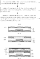
- the TFT 100 comprises an active layer 110, an amorphous silicon(a-Si) connecting layer 120 and a source-drain electrode layer 130.
- the active layer 110 includes a channel region 113, and a source region 111 and a drain region 112 which are respectively disposed on both sides of the channel region 113 and connected with the channel region 113.
- Forming materials of the channel region 113 include poly-Si.
- forming materials of the source region 111 and the drain region 112 may be poly-Si or a-Si;
- the a-Si connecting layer 120 is disposed on a side of the active layer 110 and includes a first connecting part 121 and a second connecting part 122 which are disposed to be spaced from each other;
- the source-drain electrode layer 130 includes a source electrode 131 and a drain electrode 132 which are disposed to be spaced from each other;
- the source electrode 131 is electrically connected with the source region 111 through the first connecting part 121; and the drain electrode 132 is electrically connected with the drain region 112 through the second connecting part 122.
- the source region 111 and the drain region 112 of the active layer 110 are respectively electrically connected with the source electrode 131 and the drain electrode 132 through the a-Si connecting layer 120. Therefore, compared with manufacturing process of the poly-Si TFT known by an inventor (inventors), the manufacturing process of the TFT 100 provided by the embodiments of the present invention can omit the ion implantation processes for forming a lightly doped region and a heavily doped region, and corresponding exposure processes, and has the advantages of simple manufacturing process of the TFT 100, low equipment investment, applicability for high-generation lines, and good compatibility with the production line of a-Si TFTs.
- the channel region 113 of the active layer 110 in the TFT 100 provided by the embodiment of the present invention is made from poly-Si materials (for instance, LTPS materials), and as the poly-Si materials have high electron mobility, the TFT 100 provided by the embodiment of the present invention has relatively large on-state current.
- both the source region 111 and the drain region 112 of the active layer 110 may be non-doped regions.
- forming materials of the source region 111 and the drain region 112 may both be non-doped a-Si or non-doped poly-Si.
- the source region 111 and the drain region 112 are respectively electrically connected with the source electrode 131 and the drain electrode 132 through the a-Si connecting layer 120, and both are non-doped regions.
- the TFT 100 provided by the embodiment of the present invention has relatively low OFF-state leakage current.
- the TFT 100 provided by the embodiment of the present invention has relatively lower OFF-state leakage current.
- the forming materials of the first connecting part 121 and the second connecting part 122 of the a-Si connecting layer 120 may be doped a-Si, e.g., P-doped a-Si or N-doped a-Si.
- materials of the source-drain electrode layer 130 may be metallic materials.
- the TFT 100 provided by at least one embodiment of the present invention further comprises a support substrate 100a.
- the active layer 110 may be disposed between the support substrate 100a and the source-drain electrode layer 130 in a direction perpendicular to the support substrate 100a.
- the manufacturing process of the TFT 100 can be simpler.
- the poly-Si TFT known by an inventor is a top-gate structure, so the active layer may be subjected to ion implantation doping by taking a gate electrode as a mask in the manufacturing process.
- the manufacturing process of the TFT 100 provided by the embodiment of the present invention can omit the ion implantation doping process, for instance, the TFT 100 provided by at least one embodiment of the present invention may be a bottom-gate structure. That is to say, the TFT 100 further comprises a gate electrode 140; a gate insulating layer 150 is disposed between the gate electrode 140 and the active layer 110; and the gate electrode 140 is disposed between the active layer 110 and the support substrate 100a.
- the TFT 100 may also adopt a top-gate structure.
- a plurality of thin films in the TFT 100 may be prepared by the same one exposure process.
- a distance between outer edges 110a and 110b of the active layer 110 may be substantially equal to a distance between outer edge 121a of the first connecting part 121 and outer edge 122a of the second connecting part 122.
- the active layer 110 and the a-Si connecting layer 120 may be formed by one exposure process (for instance, half-exposure process), so the number of the exposure processes can be reduced.
- a distance between outer edge 131a of the source electrode 131 and outer edge 132a of the drain electrode 132 may be substantially equal to the distance the outer edge 121a of the first connecting part 121 and the outer edge 122a of the second connecting part 122.
- the source-drain electrode layer 130, the active layer 110 and the a-Si connecting layer 120 may be formed by one exposure process (for instance, half-exposure process), so the number of the exposure processes can be further reduced.
- the distance between the outer edge 131a of the source electrode 131 and the outer edge 132a of the drain electrode 132 may be substantially equal to the distance the outer edge 121a of the first connecting part 121 and the outer edge 122a of the second connecting part 122.
- the source-drain electrode layer 130 and the a-Si connecting layer 120 may be formed by one exposure process (for instance, half-exposure process), so as to reduce the number of the exposure processes.
- a-Si connecting layer 120 is a single-layer structure as an example.
- the a-Si connecting layer 120 may also be a multi-layer structure.
- the a-Si connecting layer 120 includes a first a-Si layer 120a and a second a-Si layer 120b which are laminated to each other; the second a-Si layer 120b is disposed between the first a-Si layer 120a and the source-drain electrode layer 130; and the electrical conductivity of the second a-Si layer 120b is greater than that of the first a-Si layer 120a.
- the second a-Si layer 120b may have the function of an ohmic contact layer, so as to improve the electrical connection between the first a-Si connecting layer 120a and the source-drain electrode layer 130.
- the second a-Si layer 120b may be N-doped a-Si or P-doped a-Si.
- the first a-Si layer may be non-doped a-Si.
- the a-Si connecting layer 120 includes the first a-Si layer 120a made from the non-doped a-Si, the OFF-state leakage current of the TFT 100 can be advantageously reduced.
- the forming materials of the source region 111 and the drain region 112 may both be non-doped poly-Si.
- the TFT 100 can have relatively low OFF-state leakage current.
- At least one embodiment of the present invention further provides an array substrate 10, which comprises a plurality of TFTs 100 provided by any foregoing embodiment and disposed to be spaced to each other.
- FIG. 3 only shows one TFT 100, and the a-Si connecting layer 120 in the TFT 100 is a two-layer structure.
- the array substrate provided by the embodiment of the present invention includes but not limited to the embodiment as shown in FIG. 3 .
- the array substrate 10 may further comprise a plurality of pixel electrodes 101 disposed to be spaced to each other; the plurality of pixel electrodes 101 respectively correspond to the plurality of TFTs 100, and each pixel electrode 101 is electrically connected with a drain electrode 132 of corresponding TFT 100.
- the array substrate 10 may further comprise an insulating layer 102 covering the TFTs 100, the pixel electrode 101 may be electrically connected with the drain electrode 132 of the corresponding TFT 100 via a through hole in the insulating layer 102.
- the pixel electrode 101 may be made from indium tin oxide (ITO), indium zinc oxide (IZO) or similar transparent conductive materials. No limitation will be given here.
- the array substrate provided by the embodiment of the present invention may be an organic light-emitting diode (OLED) array substrate and may also be an array substrate applied to a liquid crystal display (LCD) device.
- the array substrate 10 may further comprise structures such as common electrode lines, gate lines and data lines. No further description will be given here.
- At least one embodiment of the present invention further provides a display device, which comprises the array substrate 10 provided by any foregoing embodiment.
- the display device may be: any product or component with display function such as an LCD panel, e-paper, an OLED panel, a mobile phone, a tablet PC, a TV, a display, a notebook computer, a digital picture frame and a navigator.
- display function such as an LCD panel, e-paper, an OLED panel, a mobile phone, a tablet PC, a TV, a display, a notebook computer, a digital picture frame and a navigator.
- At least one embodiment of the present invention further provides a method for manufacturing a TFT, which comprises: S1: forming an active layer including a channel region, a source region and a drain region, in which forming materials of the channel region include poly-Si; S2: forming an a-Si connecting layer 120 on one side of the active layer, in which the a-Si connecting layer includes a first connecting part and a second connecting part which are disposed to be spaced from each other; and S3: forming a source-drain electrode layer on a side of the a-Si connecting layer away from the active layer, in which the source-drain electrode layer includes a source electrode and a drain electrode, the source electrode is electrically connected with the source region through the first connecting part, and the drain electrode is electrically connected with the drain region through the second connecting part.
- forming the active layer may include: forming an a-Si film; and performing laser annealing treatment on a region to be formed as the channel region of the a-Si film, or a region to be formed as the channel region, a source region and a drain region of the a-Si film, so that in the region, the poly-Si may be formed.
- the poly-Si is formed by performing local laser annealing treatment on the a-Si film and compared with a manner performing laser annealing treatment on the entire a-Si film known by an inventor (inventors), the manufacturing method provided by the embodiment of the present invention can be applied to high-generation production lines.
- the orders of the steps S1 to S3 in the manufacturing method provided by the embodiment of the present invention are not limited.
- the active layer and the a-Si connecting layer may be formed by half-exposure process, namely the steps S1 and S2 may be performed simultaneously; or, the active layer, the a-Si connecting layer and the source-drain electrode layer may be formed by half-exposure process, namely the steps S1 to S3 may be performed simultaneously.
- the half-exposure process refers to a process for performing exposure treatment on a photoresist on a film via a half-tone mask or a gray-tone mask, and subsequently, forming required patterns by development and etching.
- an a-Si connecting layer film (namely a film to be formed as the a-Si connecting layer) and a source-drain electrode layer film (namely a film for forming the source-drain electrode layer) which are laminated to each other may be formed; and subsequently, the a-Si connecting layer and the source-drain electrode layer are formed by performing one exposure process on the a-Si connecting layer film and the source-drain electrode layer film. That is to say, the steps S2 and S3 may be simultaneously performed.
- steps S1 to S3 include but not limited to these enumerative orders.
- the method provided by the embodiment of the present invention may be used for manufacturing the TFT 100 provided by any foregoing embodiment.
- forming the a-Si connecting layer 120 may include: forming a first a-Si layer 120a and a second a-Si layer 120b which are laminated to each other, in which the second a-Si layer 120b is formed between the first a-Si layer 120a and the source-drain electrode layer 130, and the electrical conductivity of the second a-Si layer 120b is greater than that of the first a-Si layer 120a.
- the electrical connection between the first a-Si connecting layer 120a and the source-drain electrode layer 130 can be improved.
- the second a-Si layer 120b may be N-doped a-Si or P-doped a-Si.
- the first a-Si layer may be non-doped a-Si.
- the method may comprise the following steps S01 to S04.
- a gate electrode 140 as shown in FIG. 5a , forming a gate electrode 140, a gate insulating layer 150 and an a-Si film 110' on a support substrate 100a (e.g., a glass substrate) in sequence.
- a support substrate 100a e.g., a glass substrate
- the gate electrode 140 is formed by processes such as deposition, exposure and etching; the gate insulating layer 150 is formed by deposited, for instance, a silicon nitride layer and a silicon dioxide layer; and then, the a-Si film 110' is deposited.
- a-Si connecting layer film 120' depositing an a-Si connecting layer film 120' and a source-drain electrode layer film 130' on the support substrate 100a obtained after the step S02 in sequence, in which the a-Si connecting layer film 120' includes a film 120a' (e.g., non-doped a-Si, hereafter referred to as a-Si) for forming the first a-Si layer and a film 120b' (for instance, doped a-Si, e.g., N-doped a-Si, hereafter referred to as n+a-Si) for forming the second a-Si layer which are deposited in sequence.
- a-Si connecting layer film 120' includes a film 120a' (e.g., non-doped a-Si, hereafter referred to as a-Si) for forming the first a-Si layer and a film 120b' (for instance, doped a-S
- At least one embodiment of the present invention further provides a method for manufacturing an array substrate, which comprises: forming a plurality of TFTs disposed to be spaced to each other.
- the TFT is manufactured by using the manufacturing method provided by any foregoing embodiment.
- the TFT may be the TFT 100 provided by any foregoing embodiment.
- the method provided by the embodiment of the present invention may further comprise: forming an insulating layer 102 for covering the TFT 100, and a through hole (not shown in FIG. 6 ) disposed in the insulating layer 102; and forming a pixel electrode 101, in which the pixel electrode 101 are electrically connected with a drain electrode 132 of the TFT 100 via the through hole in the insulating layer 102.
- the manufacturing method provided by the embodiment of the present invention is applicable to various display modes such as twisted nematic (TN), vertical alignment (VA), in-plane switch (IPS) and advanced super dimension switch (ADS).
- TN twisted nematic
- VA vertical alignment
- IPS in-plane switch
- ADS advanced super dimension switch
- the manufacturing method provided by the embodiment of the present invention further comprises other steps.
- gate lines and common electrode lines may also be formed in a process of forming the gate electrode 140 of the TFT 100.
- data lines may also be formed in a process of forming the source electrode 131 and the drain electrode 132 of the TFT 100.
- common electrodes may also be formed and are electrically connected with the common electrode lines. No further description will be given here.
- a TFT 200 which comprises an active layer 210 and a source-drain electrode layer 230.
- the active layer 210 includes a channel region 213, and a source region 211 and a drain region 212 which are respectively disposed on both sides of the channel region 213 and connected with the channel region 213; forming materials of the channel region 213 include poly-Si; forming materials of the source region 211 and the drain region 212 include doped a-Si (e.g., N-doped a-Si or P-doped a-Si);
- the source-drain electrode layer 230 is disposed on a side of the active layer 210 and includes a source electrode 231 and a drain electrode 232 which are disposed to be spaced from each other; the source electrode 231 is electrically connected with the source region 211; and the drain electrode 232 is electrically connected with the drain region 212.
- the manufacturing method of the active layer 210 may include: forming an a-Si film; performing a laser annealing treatment on a region to be formed as the channel region 213 of the a-Si film to form poly-Si, and then removing a remaining portion of the a-Si film by processes such as exposure and etching; forming a doped a-Si film on the poly-Si channel region (for instance, the doped a-Si film may be formed directly by deposition), and performing processes such as exposure and etching to the doped a-Si film to form the source region 211 and the drain region 212 connected with the channel region 213, thus, forming the active layer 210.
- the active layer 210 may also be formed by other means.
- the source region 211 and the drain region 212 of the active layer 210 are made from doped a-Si materials, so as to be respectively electrically connected with the source electrode 131 and the drain electrode 132. Therefore, compared with the manufacturing process of the poly-Si TFT known by an inventor (inventors), the manufacturing process of the TFT 200 provided by the embodiment of the present invention can omit the ion implantation processes for forming the lightly and heavily doped regions, and corresponding exposure processes, so the manufacturing process of the TFT 200 has the advantages of simple processes, low equipment investment, applicability to high-generation lines, and good compatibility with the production line of the a-Si TFT.
- the channel region 213 of the active layer 210 in the TFT 200 provided by the embodiment of the present invention is made from poly-Si materials (for instance, LTPS materials), and as the poly-Si materials have relatively high electron mobility, the TFT 200 provided by the embodiment of the present invention has relatively large on-state current.
- the TFT 200 further comprises a support substrate 200a.
- the channel region 213, the source region 211 and the source electrode 131 may be overlapped at the same position, and the channel region 213, the drain region 212 and the drain electrode 132 may also be overlapped at the same position.
- the electrical connection between the channel region, the source-drain regions and the source-drain electrodes can be improved.
- the TFT 200 provided by the embodiment of the present invention may further comprise structures such as a support substrate 200a, a gate electrode 240, and a gate insulating layer 250 disposed between the gate electrode 240 and the active layer 210.
- the TFT and the manufacturing method thereof, the array substrate and the manufacturing method thereof, and the display device, provided by the embodiments of the present invention at least have one of the following advantages.
- the embodiments of the TFT and the manufacturing method thereof, the array substrate and the manufacturing method thereof, and the display device may refer to each other.
- the embodiments of the present invention and the characteristics in the embodiments may be mutually combined without conflict.
Landscapes
- Thin Film Transistor (AREA)
- Liquid Crystal (AREA)
- Chemical & Material Sciences (AREA)
- Crystallography & Structural Chemistry (AREA)
Claims (13)
- Dünnschichttransistor, TFT, (100, 200), mit:einer aktiven Schicht (110, 210), die einen Kanalbereich (113, 213), einen Source-Bereich (111, 211) und einen Drain-Bereich (112, 212) aufweist, wobei die Materialien, die den Kanalbereich (113, 213) bilden, polykristallines Silizium, poly-Si, enthalteneiner Verbindungsschicht (120) aus amorphem Silizium, a-Si, die auf einer Seite der aktiven Schicht (110) angeordnet ist und einen ersten Verbindungsteil (121) und einen zweiten Verbindungsteil (122) aufweist, die so angeordnet sind, dass sie voneinander beabstandet sind; undeine Source-Drain-Elektrodenschicht (130, 230), die eine Source-Elektrode (131, 231) und eine Drain-Elektrode (132, 232) aufweist, die so angeordnet sind, dass sie voneinander beabstandet sind,wobei die Source-Elektrode (131) über den ersten Verbindungsteil (121) elektrisch mit dem Source-Bereich (111) verbunden ist und die Drain-Elektrode (132) über den zweiten Verbindungsteil (122) elektrisch mit dem Drain-Bereich (112) verbunden ist,wobei die a-Si-Verbindungsschicht (120) eine erste a-Si-Schicht (120a) und eine zweite a-Si-Schicht (120b) aufweist, die miteinander laminiert sind, wobei die zweite a-Si-Schicht (120b) zwischen der ersten a-Si-Schicht (120a) und der Source-Drain-Elektrodenschicht (130) angeordnet ist, wobei die gesamte erste a-Si-Schicht (120a) mit der aktiven Schicht (110) in Kontakt steht,dadurch gekennzeichnet, dass eine elektrische Leitfähigkeit der zweiten a-Si-Schicht (120b), die mit der Source-Drain-Elektrodenschicht (130) in Kontakt steht, größer ist als die der ersten a-Si-Schicht (120a), die mit der aktiven Schicht (110) in Kontakt steht.
- TFT nach Anspruch 1, wobei sowohl der Source-Bereich (111) als auch der Drain-Bereich (112) nicht-dotierte Bereiche sind.
- TFT nach Anspruch 1, wobei die Bildungsmaterialien der ersten a-Si-Schicht (120a) nicht dotiertes a-Si sind.
- TFT nach einem der Ansprüche 1 bis 3, wobei ein Abstand zwischen Außenkanten (110a, 110b) der aktiven Schicht (110) im Wesentlichen gleich einem Abstand zwischen einer Außenkante (121a) des ersten Verbindungsteils (121) und einer Außenkante (122a) des zweiten Verbindungsteils (122) in einer Richtung vom Source-Bereich (111) zum Drain-Bereich (112) ist.
- TFT nach Anspruch 4, wobei ein Abstand zwischen einer Außenkante (131a) der Source-Elektrode (131) und einer Außenkante (132a) der Drain-Elektrode (132) im Wesentlichen gleich dem Abstand zwischen der Außenkante (121a) des ersten Verbindungsteils (121) und der Außenkante (122a) des zweiten Verbindungsteils (122) ist.
- TFT nach einem der Ansprüche 1 bis 4, wobei ein Abstand zwischen einer Außenkante (131a) der Source-Elektrode (131) und einer Außenkante (132a) der Drain-Elektrode (132) gleich einem Abstand zwischen einer Außenkante (121a) des ersten Verbindungsteils (121) und einer Außenkante (122a) des zweiten Verbindungsteils (122) ist.
- Array-Substrat (10), das eine Vielzahl von TFTs (100, 200) nach einem der Ansprüche 1 bis 6 aufweist, wobei die Vielzahl von TFTs (100, 200) so angeordnet ist, dass sie einen Abstand zueinander haben.
- Array-Substrat (10) nach Anspruch 7, das ferner eine Vielzahl von Pixelelektroden (101) aufweist, die so angeordnet sind, dass sie voneinander beabstandet sind, wobei die Vielzahl von Pixelelektroden (101) jeweils der Vielzahl von TFTs (100) entspricht und jede der Vielzahl von Pixelelektroden (101) elektrisch mit einer Drain-Elektrode (132) eines entsprechenden der Vielzahl von TFTs (100) verbunden ist.
- Anzeigevorrichtung, die das Array-Substrat (10) nach Anspruch 7 oder 8 aufweist.
- Verfahren zur Herstellung eines TFT (100), mit:Bilden einer aktiven Schicht (110) mit einem Kanalbereich (113), einem Source-Bereich (111) und einem Drain-Bereich (112), wobei die Bildungsmaterialien des Kanalbereichs (113) Poly-Si enthalten;Bilden einer a-Si-Verbindungsschicht (120) auf einer Seite der aktiven Schicht (110), wobei die a-Si-Verbindungsschicht (120) einen ersten Verbindungsteil (121) und einen zweiten Verbindungsteil (122) aufweist, die so angeordnet sind, dass sie voneinander beabstandet sind; undBilden einer Source-Drain-Elektrodenschicht (130) auf einer von der aktiven Schicht (110) abgewandten Seite der a-Si-Verbindungsschicht (120), wobei die Source-Drain-Elektrodenschicht (130) eine Source-Elektrode (131) und eine Drain-Elektrode (132) aufweist, die Source-Elektrode (131) über den ersten Verbindungsteil (121) elektrisch mit dem Source-Bereich (111) verbunden ist und die Drain-Elektrode (132) über den zweiten Verbindungsteil (122) elektrisch mit dem Drain-Bereich (112) verbunden ist,wobei das Bilden der a-Si-Verbindungsschicht (120) das Bilden einer ersten a-Si-Schicht (120a) und einer zweiten a-Si-Schicht (120b) aufweist, die aneinander laminiert sind, wobei die zweite a-Si-Schicht (120b) zwischen der ersten a-Si-Schicht (120a) und der Source-Drain-Elektrodenschicht (130) gebildet ist, wobei die gesamte erste a-Si-Schicht (120a) mit der aktiven Schicht (110) in Kontakt steht,dadurch gekennzeichnet, dass eine elektrische Leitfähigkeit der zweiten a-Si-Schicht (120b), die mit der Source-Drain-Elektrodenschicht (130) in Kontakt steht, größer ist als die der ersten a-Si-Schicht (120a), die mit der aktiven Schicht (110) in Kontakt steht.
- Herstellungsverfahren nach Anspruch 10, wobei das Bilden der aktiven Schicht (110) aufweistBilden einer a-Si-Dünnschicht (110'); undDurchführen einer Laser-Glühbehandlung an einem Bereich, der als der Kanalbereich (113) der a-Si-Dünnschicht (110') gebildet werden soll, oder an einem Bereich, der als der Kanalbereich (113), der Source-Bereich (111) und der Drain-Bereich (112) der a-Si-Dünnschicht (110') gebildet werden soll, um so Poly-Si in dem Bereich zu bilden.
- Herstellungsverfahren nach einem der Ansprüche 10 bis 11, wobeidie aktive Schicht (110) und die a-Si-Verbindungsschicht (120) durch einen Halbbelichtungsprozess gebildet werden; oderdie aktive Schicht (110), die a-Si-Verbindungsschicht (120) und die Source-Drain-Elektrodenschicht (130) durch einen Halbbelichtungsprozess gebildet werden.
- Verfahren zur Herstellung eines Array-Substrats (10), mit:
Bilden einer Vielzahl von TFTs (100), die so angeordnet sind, dass sie voneinander beabstandet sind, wobei die TFTs (100) durch das Herstellungsverfahren nach einem der Ansprüche 10 bis 12 hergestellt werden.
Applications Claiming Priority (2)
| Application Number | Priority Date | Filing Date | Title |
|---|---|---|---|
| CN201610311349.6A CN105870198B (zh) | 2016-05-11 | 2016-05-11 | 薄膜晶体管及制作方法、阵列基板及制作方法和显示装置 |
| PCT/CN2017/074772 WO2017193667A1 (zh) | 2016-05-11 | 2017-02-24 | 薄膜晶体管及制作方法、阵列基板及制作方法和显示装置 |
Publications (3)
| Publication Number | Publication Date |
|---|---|
| EP3457441A1 EP3457441A1 (de) | 2019-03-20 |
| EP3457441A4 EP3457441A4 (de) | 2019-12-11 |
| EP3457441B1 true EP3457441B1 (de) | 2022-04-20 |
Family
ID=56631799
Family Applications (1)
| Application Number | Title | Priority Date | Filing Date |
|---|---|---|---|
| EP17761424.5A Active EP3457441B1 (de) | 2016-05-11 | 2017-02-24 | Dünnschichttransistor und herstellungsverfahren dafür, arraysubstrat und herstellungsverfahren dafür sowie anzeigevorrichtung |
Country Status (4)
| Country | Link |
|---|---|
| US (1) | US10403756B2 (de) |
| EP (1) | EP3457441B1 (de) |
| CN (1) | CN105870198B (de) |
| WO (1) | WO2017193667A1 (de) |
Families Citing this family (8)
| Publication number | Priority date | Publication date | Assignee | Title |
|---|---|---|---|---|
| CN105870198B (zh) | 2016-05-11 | 2020-03-31 | 京东方科技集团股份有限公司 | 薄膜晶体管及制作方法、阵列基板及制作方法和显示装置 |
| CN107863355B (zh) * | 2017-10-26 | 2022-01-25 | 上海中航光电子有限公司 | 一种显示基板、显示装置和显示基板的制造方法 |
| US10672797B2 (en) * | 2018-09-30 | 2020-06-02 | Chongqing Hkc Optoelectronics Technology Co., Ltd. | Array substrate, method for fabricating array substrate and display |
| CN109300991B (zh) * | 2018-09-30 | 2021-12-24 | 京东方科技集团股份有限公司 | 薄膜晶体管及其制备方法、阵列基板、显示面板及装置 |
| CN109411531B (zh) * | 2018-10-18 | 2022-04-19 | 京东方科技集团股份有限公司 | 一种薄膜晶体管及其制作方法、阵列基板、显示装置 |
| CN109390412A (zh) * | 2018-10-24 | 2019-02-26 | 合肥鑫晟光电科技有限公司 | 晶体管及其制造方法、显示基板、显示装置 |
| CN109411547B (zh) * | 2018-10-31 | 2022-10-11 | 合肥鑫晟光电科技有限公司 | 薄膜晶体管及制备方法、显示基板及制备方法、显示装置 |
| CN114823724B (zh) * | 2022-04-11 | 2026-01-27 | 京东方科技集团股份有限公司 | 一种显示基板及其制作方法和显示装置 |
Family Cites Families (12)
| Publication number | Priority date | Publication date | Assignee | Title |
|---|---|---|---|---|
| JPS63299276A (ja) * | 1987-05-29 | 1988-12-06 | Seiko Epson Corp | 薄膜トランジスタ |
| US6794682B2 (en) * | 2001-04-04 | 2004-09-21 | Canon Kabushiki Kaisha | Semiconductor device, method for manufacturing the same, and radiation detector |
| KR100573225B1 (ko) * | 2003-09-24 | 2006-04-24 | 엘지.필립스 엘시디 주식회사 | 비정질 실리콘층의 결정화 방법 |
| KR100841365B1 (ko) * | 2006-12-06 | 2008-06-26 | 삼성에스디아이 주식회사 | 박막트랜지스터와 그 제조방법 및 이를 구비한유기전계발광표시장치 |
| TW201037757A (en) * | 2009-04-14 | 2010-10-16 | Au Optronics Corp | Semiconductor stacking layer and fabricating method thereof |
| KR101790176B1 (ko) * | 2010-11-02 | 2017-10-25 | 엘지디스플레이 주식회사 | 어레이 기판의 제조방법 |
| KR101757443B1 (ko) | 2010-12-08 | 2017-07-13 | 엘지디스플레이 주식회사 | 미세 결정 실리콘 박막 트랜지스터와 이를 포함하는 표시장치 및 그 제조 방법 |
| CN103456739A (zh) * | 2013-08-16 | 2013-12-18 | 北京京东方光电科技有限公司 | 阵列基板及其制造方法和显示装置 |
| CN104779301B (zh) * | 2015-04-24 | 2017-10-27 | 京东方科技集团股份有限公司 | 一种薄膜晶体管及其制作方法、阵列基板、显示装置 |
| CN105070724A (zh) * | 2015-07-16 | 2015-11-18 | 深圳市华星光电技术有限公司 | Tft基板的制作方法及制得的tft基板 |
| CN105870198B (zh) | 2016-05-11 | 2020-03-31 | 京东方科技集团股份有限公司 | 薄膜晶体管及制作方法、阵列基板及制作方法和显示装置 |
| CN205582944U (zh) * | 2016-05-11 | 2016-09-14 | 京东方科技集团股份有限公司 | 薄膜晶体管、阵列基板和显示装置 |
-
2016
- 2016-05-11 CN CN201610311349.6A patent/CN105870198B/zh active Active
-
2017
- 2017-02-24 US US15/558,104 patent/US10403756B2/en active Active
- 2017-02-24 WO PCT/CN2017/074772 patent/WO2017193667A1/zh not_active Ceased
- 2017-02-24 EP EP17761424.5A patent/EP3457441B1/de active Active
Also Published As
| Publication number | Publication date |
|---|---|
| US10403756B2 (en) | 2019-09-03 |
| CN105870198A (zh) | 2016-08-17 |
| US20180358473A1 (en) | 2018-12-13 |
| EP3457441A1 (de) | 2019-03-20 |
| EP3457441A4 (de) | 2019-12-11 |
| CN105870198B (zh) | 2020-03-31 |
| WO2017193667A1 (zh) | 2017-11-16 |
Similar Documents
| Publication | Publication Date | Title |
|---|---|---|
| EP3457441B1 (de) | Dünnschichttransistor und herstellungsverfahren dafür, arraysubstrat und herstellungsverfahren dafür sowie anzeigevorrichtung | |
| US10895774B2 (en) | Array substrate, manufacturing method, display panel and display device | |
| US10490670B2 (en) | Manufacturing method of array substrate, array substrate with active layer being above first electrode, and display device | |
| US10367073B2 (en) | Thin film transistor (TFT) with structured gate insulator | |
| US9324735B2 (en) | Array substrate and manufacturing method thereof, display panel and display device | |
| US10340354B2 (en) | Manufacturing method of thin-film transistor (TFT) array substrate | |
| US9312146B2 (en) | Manufacturing method of a thin film transistor | |
| US20160276376A1 (en) | Array substrate, method for fabricating the same, and display device | |
| US9620646B2 (en) | Array substrate, manufacturing method thereof and display device | |
| US10050151B2 (en) | Dual-gate TFT array substrate and manufacturing method thereof, and display device | |
| US20170255044A1 (en) | Tft substrates and the manufacturing methods thereof | |
| CN203521413U (zh) | 一种阵列基板及显示装置 | |
| US20170186784A1 (en) | TFT and Manufacturing Method Thereof, Array Substrate and Manufacturing Method Thereof, and Display Device | |
| US20170170330A1 (en) | Thin film transistors (tfts), manufacturing methods of tfts, and display devices | |
| KR20180098621A (ko) | 저온 폴리실리콘 어레이 기판의 제조방법 | |
| CN107611139B (zh) | 薄膜晶体管阵列基板及制作方法 | |
| CN203871327U (zh) | 一种阵列基板及显示装置 | |
| US20180190831A1 (en) | Thin film transistor and method for manufacturing the same, array substrate and display device | |
| US10978495B2 (en) | Array substrate and method of manufacturing the same, and display device | |
| US20170373181A1 (en) | Metal oxide thin film transistors (tfts) and the manufacturing method thereof | |
| WO2015000255A1 (zh) | 阵列基板、显示装置及阵列基板的制造方法 | |
| US9276014B2 (en) | Array substrate and method of fabricating the same, and liquid crystal display device | |
| US10109654B2 (en) | Manufacturing method of display substrate, display substrate and display device | |
| US9972643B2 (en) | Array substrate and fabrication method thereof, and display device | |
| CN114402430B (zh) | 阵列基板及制作方法、显示面板 |
Legal Events
| Date | Code | Title | Description |
|---|---|---|---|
| STAA | Information on the status of an ep patent application or granted ep patent |
Free format text: STATUS: UNKNOWN |
|
| STAA | Information on the status of an ep patent application or granted ep patent |
Free format text: STATUS: THE INTERNATIONAL PUBLICATION HAS BEEN MADE |
|
| PUAI | Public reference made under article 153(3) epc to a published international application that has entered the european phase |
Free format text: ORIGINAL CODE: 0009012 |
|
| STAA | Information on the status of an ep patent application or granted ep patent |
Free format text: STATUS: REQUEST FOR EXAMINATION WAS MADE |
|
| 17P | Request for examination filed |
Effective date: 20170913 |
|
| AK | Designated contracting states |
Kind code of ref document: A1 Designated state(s): AL AT BE BG CH CY CZ DE DK EE ES FI FR GB GR HR HU IE IS IT LI LT LU LV MC MK MT NL NO PL PT RO RS SE SI SK SM TR |
|
| AX | Request for extension of the european patent |
Extension state: BA ME |
|
| DAV | Request for validation of the european patent (deleted) | ||
| DAX | Request for extension of the european patent (deleted) | ||
| A4 | Supplementary search report drawn up and despatched |
Effective date: 20191111 |
|
| RIC1 | Information provided on ipc code assigned before grant |
Ipc: H01L 21/77 20170101ALI20191105BHEP Ipc: H01L 27/12 20060101ALI20191105BHEP Ipc: H01L 21/336 20060101ALI20191105BHEP Ipc: H01L 29/10 20060101ALI20191105BHEP Ipc: H01L 29/786 20060101AFI20191105BHEP Ipc: H01L 29/08 20060101ALI20191105BHEP |
|
| GRAP | Despatch of communication of intention to grant a patent |
Free format text: ORIGINAL CODE: EPIDOSNIGR1 |
|
| STAA | Information on the status of an ep patent application or granted ep patent |
Free format text: STATUS: GRANT OF PATENT IS INTENDED |
|
| INTG | Intention to grant announced |
Effective date: 20220104 |
|
| GRAS | Grant fee paid |
Free format text: ORIGINAL CODE: EPIDOSNIGR3 |
|
| GRAA | (expected) grant |
Free format text: ORIGINAL CODE: 0009210 |
|
| STAA | Information on the status of an ep patent application or granted ep patent |
Free format text: STATUS: THE PATENT HAS BEEN GRANTED |
|
| AK | Designated contracting states |
Kind code of ref document: B1 Designated state(s): AL AT BE BG CH CY CZ DE DK EE ES FI FR GB GR HR HU IE IS IT LI LT LU LV MC MK MT NL NO PL PT RO RS SE SI SK SM TR |
|
| REG | Reference to a national code |
Ref country code: GB Ref legal event code: FG4D |
|
| REG | Reference to a national code |
Ref country code: CH Ref legal event code: EP |
|
| REG | Reference to a national code |
Ref country code: DE Ref legal event code: R096 Ref document number: 602017056266 Country of ref document: DE |
|
| REG | Reference to a national code |
Ref country code: IE Ref legal event code: FG4D |
|
| REG | Reference to a national code |
Ref country code: AT Ref legal event code: REF Ref document number: 1485888 Country of ref document: AT Kind code of ref document: T Effective date: 20220515 |
|
| REG | Reference to a national code |
Ref country code: LT Ref legal event code: MG9D |
|
| REG | Reference to a national code |
Ref country code: NL Ref legal event code: MP Effective date: 20220420 |
|
| REG | Reference to a national code |
Ref country code: AT Ref legal event code: MK05 Ref document number: 1485888 Country of ref document: AT Kind code of ref document: T Effective date: 20220420 |
|
| PG25 | Lapsed in a contracting state [announced via postgrant information from national office to epo] |
Ref country code: NL Free format text: LAPSE BECAUSE OF FAILURE TO SUBMIT A TRANSLATION OF THE DESCRIPTION OR TO PAY THE FEE WITHIN THE PRESCRIBED TIME-LIMIT Effective date: 20220420 |
|
| PG25 | Lapsed in a contracting state [announced via postgrant information from national office to epo] |
Ref country code: SE Free format text: LAPSE BECAUSE OF FAILURE TO SUBMIT A TRANSLATION OF THE DESCRIPTION OR TO PAY THE FEE WITHIN THE PRESCRIBED TIME-LIMIT Effective date: 20220420 Ref country code: PT Free format text: LAPSE BECAUSE OF FAILURE TO SUBMIT A TRANSLATION OF THE DESCRIPTION OR TO PAY THE FEE WITHIN THE PRESCRIBED TIME-LIMIT Effective date: 20220822 Ref country code: NO Free format text: LAPSE BECAUSE OF FAILURE TO SUBMIT A TRANSLATION OF THE DESCRIPTION OR TO PAY THE FEE WITHIN THE PRESCRIBED TIME-LIMIT Effective date: 20220720 Ref country code: LT Free format text: LAPSE BECAUSE OF FAILURE TO SUBMIT A TRANSLATION OF THE DESCRIPTION OR TO PAY THE FEE WITHIN THE PRESCRIBED TIME-LIMIT Effective date: 20220420 Ref country code: HR Free format text: LAPSE BECAUSE OF FAILURE TO SUBMIT A TRANSLATION OF THE DESCRIPTION OR TO PAY THE FEE WITHIN THE PRESCRIBED TIME-LIMIT Effective date: 20220420 Ref country code: GR Free format text: LAPSE BECAUSE OF FAILURE TO SUBMIT A TRANSLATION OF THE DESCRIPTION OR TO PAY THE FEE WITHIN THE PRESCRIBED TIME-LIMIT Effective date: 20220721 Ref country code: FI Free format text: LAPSE BECAUSE OF FAILURE TO SUBMIT A TRANSLATION OF THE DESCRIPTION OR TO PAY THE FEE WITHIN THE PRESCRIBED TIME-LIMIT Effective date: 20220420 Ref country code: ES Free format text: LAPSE BECAUSE OF FAILURE TO SUBMIT A TRANSLATION OF THE DESCRIPTION OR TO PAY THE FEE WITHIN THE PRESCRIBED TIME-LIMIT Effective date: 20220420 Ref country code: BG Free format text: LAPSE BECAUSE OF FAILURE TO SUBMIT A TRANSLATION OF THE DESCRIPTION OR TO PAY THE FEE WITHIN THE PRESCRIBED TIME-LIMIT Effective date: 20220720 Ref country code: AT Free format text: LAPSE BECAUSE OF FAILURE TO SUBMIT A TRANSLATION OF THE DESCRIPTION OR TO PAY THE FEE WITHIN THE PRESCRIBED TIME-LIMIT Effective date: 20220420 |
|
| PG25 | Lapsed in a contracting state [announced via postgrant information from national office to epo] |
Ref country code: RS Free format text: LAPSE BECAUSE OF FAILURE TO SUBMIT A TRANSLATION OF THE DESCRIPTION OR TO PAY THE FEE WITHIN THE PRESCRIBED TIME-LIMIT Effective date: 20220420 Ref country code: PL Free format text: LAPSE BECAUSE OF FAILURE TO SUBMIT A TRANSLATION OF THE DESCRIPTION OR TO PAY THE FEE WITHIN THE PRESCRIBED TIME-LIMIT Effective date: 20220420 Ref country code: LV Free format text: LAPSE BECAUSE OF FAILURE TO SUBMIT A TRANSLATION OF THE DESCRIPTION OR TO PAY THE FEE WITHIN THE PRESCRIBED TIME-LIMIT Effective date: 20220420 Ref country code: IS Free format text: LAPSE BECAUSE OF FAILURE TO SUBMIT A TRANSLATION OF THE DESCRIPTION OR TO PAY THE FEE WITHIN THE PRESCRIBED TIME-LIMIT Effective date: 20220820 |
|
| REG | Reference to a national code |
Ref country code: DE Ref legal event code: R097 Ref document number: 602017056266 Country of ref document: DE |
|
| PG25 | Lapsed in a contracting state [announced via postgrant information from national office to epo] |
Ref country code: SM Free format text: LAPSE BECAUSE OF FAILURE TO SUBMIT A TRANSLATION OF THE DESCRIPTION OR TO PAY THE FEE WITHIN THE PRESCRIBED TIME-LIMIT Effective date: 20220420 Ref country code: SK Free format text: LAPSE BECAUSE OF FAILURE TO SUBMIT A TRANSLATION OF THE DESCRIPTION OR TO PAY THE FEE WITHIN THE PRESCRIBED TIME-LIMIT Effective date: 20220420 Ref country code: RO Free format text: LAPSE BECAUSE OF FAILURE TO SUBMIT A TRANSLATION OF THE DESCRIPTION OR TO PAY THE FEE WITHIN THE PRESCRIBED TIME-LIMIT Effective date: 20220420 Ref country code: EE Free format text: LAPSE BECAUSE OF FAILURE TO SUBMIT A TRANSLATION OF THE DESCRIPTION OR TO PAY THE FEE WITHIN THE PRESCRIBED TIME-LIMIT Effective date: 20220420 Ref country code: DK Free format text: LAPSE BECAUSE OF FAILURE TO SUBMIT A TRANSLATION OF THE DESCRIPTION OR TO PAY THE FEE WITHIN THE PRESCRIBED TIME-LIMIT Effective date: 20220420 Ref country code: CZ Free format text: LAPSE BECAUSE OF FAILURE TO SUBMIT A TRANSLATION OF THE DESCRIPTION OR TO PAY THE FEE WITHIN THE PRESCRIBED TIME-LIMIT Effective date: 20220420 |
|
| PLBE | No opposition filed within time limit |
Free format text: ORIGINAL CODE: 0009261 |
|
| STAA | Information on the status of an ep patent application or granted ep patent |
Free format text: STATUS: NO OPPOSITION FILED WITHIN TIME LIMIT |
|
| 26N | No opposition filed |
Effective date: 20230123 |
|
| PG25 | Lapsed in a contracting state [announced via postgrant information from national office to epo] |
Ref country code: AL Free format text: LAPSE BECAUSE OF FAILURE TO SUBMIT A TRANSLATION OF THE DESCRIPTION OR TO PAY THE FEE WITHIN THE PRESCRIBED TIME-LIMIT Effective date: 20220420 |
|
| PG25 | Lapsed in a contracting state [announced via postgrant information from national office to epo] |
Ref country code: SI Free format text: LAPSE BECAUSE OF FAILURE TO SUBMIT A TRANSLATION OF THE DESCRIPTION OR TO PAY THE FEE WITHIN THE PRESCRIBED TIME-LIMIT Effective date: 20220420 |
|
| PG25 | Lapsed in a contracting state [announced via postgrant information from national office to epo] |
Ref country code: MC Free format text: LAPSE BECAUSE OF FAILURE TO SUBMIT A TRANSLATION OF THE DESCRIPTION OR TO PAY THE FEE WITHIN THE PRESCRIBED TIME-LIMIT Effective date: 20220420 |
|
| REG | Reference to a national code |
Ref country code: CH Ref legal event code: PL |
|
| REG | Reference to a national code |
Ref country code: BE Ref legal event code: MM Effective date: 20230228 |
|
| PG25 | Lapsed in a contracting state [announced via postgrant information from national office to epo] |
Ref country code: LU Free format text: LAPSE BECAUSE OF NON-PAYMENT OF DUE FEES Effective date: 20230224 Ref country code: LI Free format text: LAPSE BECAUSE OF NON-PAYMENT OF DUE FEES Effective date: 20230228 Ref country code: CH Free format text: LAPSE BECAUSE OF NON-PAYMENT OF DUE FEES Effective date: 20230228 |
|
| REG | Reference to a national code |
Ref country code: IE Ref legal event code: MM4A |
|
| PG25 | Lapsed in a contracting state [announced via postgrant information from national office to epo] |
Ref country code: IT Free format text: LAPSE BECAUSE OF FAILURE TO SUBMIT A TRANSLATION OF THE DESCRIPTION OR TO PAY THE FEE WITHIN THE PRESCRIBED TIME-LIMIT Effective date: 20220420 Ref country code: IE Free format text: LAPSE BECAUSE OF NON-PAYMENT OF DUE FEES Effective date: 20230224 Ref country code: FR Free format text: LAPSE BECAUSE OF NON-PAYMENT OF DUE FEES Effective date: 20230228 |
|
| PG25 | Lapsed in a contracting state [announced via postgrant information from national office to epo] |
Ref country code: BE Free format text: LAPSE BECAUSE OF NON-PAYMENT OF DUE FEES Effective date: 20230228 |
|
| PG25 | Lapsed in a contracting state [announced via postgrant information from national office to epo] |
Ref country code: BG Free format text: LAPSE BECAUSE OF FAILURE TO SUBMIT A TRANSLATION OF THE DESCRIPTION OR TO PAY THE FEE WITHIN THE PRESCRIBED TIME-LIMIT Effective date: 20220420 |
|
| REG | Reference to a national code |
Ref country code: DE Ref legal event code: R079 Ref document number: 602017056266 Country of ref document: DE Free format text: PREVIOUS MAIN CLASS: H01L0029786000 Ipc: H10D0030670000 |
|
| PG25 | Lapsed in a contracting state [announced via postgrant information from national office to epo] |
Ref country code: BG Free format text: LAPSE BECAUSE OF FAILURE TO SUBMIT A TRANSLATION OF THE DESCRIPTION OR TO PAY THE FEE WITHIN THE PRESCRIBED TIME-LIMIT Effective date: 20220420 |
|
| PGFP | Annual fee paid to national office [announced via postgrant information from national office to epo] |
Ref country code: DE Payment date: 20250218 Year of fee payment: 9 |
|
| PGFP | Annual fee paid to national office [announced via postgrant information from national office to epo] |
Ref country code: GB Payment date: 20250220 Year of fee payment: 9 |
|
| PG25 | Lapsed in a contracting state [announced via postgrant information from national office to epo] |
Ref country code: CY Free format text: LAPSE BECAUSE OF FAILURE TO SUBMIT A TRANSLATION OF THE DESCRIPTION OR TO PAY THE FEE WITHIN THE PRESCRIBED TIME-LIMIT; INVALID AB INITIO Effective date: 20170224 |
|
| PG25 | Lapsed in a contracting state [announced via postgrant information from national office to epo] |
Ref country code: HU Free format text: LAPSE BECAUSE OF FAILURE TO SUBMIT A TRANSLATION OF THE DESCRIPTION OR TO PAY THE FEE WITHIN THE PRESCRIBED TIME-LIMIT; INVALID AB INITIO Effective date: 20170224 |
|
| PG25 | Lapsed in a contracting state [announced via postgrant information from national office to epo] |
Ref country code: TR Free format text: LAPSE BECAUSE OF FAILURE TO SUBMIT A TRANSLATION OF THE DESCRIPTION OR TO PAY THE FEE WITHIN THE PRESCRIBED TIME-LIMIT Effective date: 20220420 |