EP3451564B1 - Error correction methods and apparatus - Google Patents
Error correction methods and apparatus Download PDFInfo
- Publication number
- EP3451564B1 EP3451564B1 EP18195190.6A EP18195190A EP3451564B1 EP 3451564 B1 EP3451564 B1 EP 3451564B1 EP 18195190 A EP18195190 A EP 18195190A EP 3451564 B1 EP3451564 B1 EP 3451564B1
- Authority
- EP
- European Patent Office
- Prior art keywords
- transmission
- data
- coded data
- section
- error correction
- Prior art date
- Legal status (The legal status is an assumption and is not a legal conclusion. Google has not performed a legal analysis and makes no representation as to the accuracy of the status listed.)
- Active
Links
Images


Classifications
-
- H—ELECTRICITY
- H04—ELECTRIC COMMUNICATION TECHNIQUE
- H04L—TRANSMISSION OF DIGITAL INFORMATION, e.g. TELEGRAPHIC COMMUNICATION
- H04L1/00—Arrangements for detecting or preventing errors in the information received
- H04L1/004—Arrangements for detecting or preventing errors in the information received by using forward error control
- H04L1/0056—Systems characterized by the type of code used
- H04L1/0057—Block codes
-
- H—ELECTRICITY
- H04—ELECTRIC COMMUNICATION TECHNIQUE
- H04L—TRANSMISSION OF DIGITAL INFORMATION, e.g. TELEGRAPHIC COMMUNICATION
- H04L25/00—Baseband systems
- H04L25/02—Details ; arrangements for supplying electrical power along data transmission lines
- H04L25/14—Channel dividing arrangements, i.e. in which a single bit stream is divided between several baseband channels and reassembled at the receiver
-
- H—ELECTRICITY
- H04—ELECTRIC COMMUNICATION TECHNIQUE
- H04L—TRANSMISSION OF DIGITAL INFORMATION, e.g. TELEGRAPHIC COMMUNICATION
- H04L1/00—Arrangements for detecting or preventing errors in the information received
- H04L2001/0092—Error control systems characterised by the topology of the transmission link
- H04L2001/0096—Channel splitting in point-to-point links
Definitions
- This invention relates to a transmission apparatus, a transmission method, a reception apparatus, a reception method, a program and a transmission system.
- Serial ATA High Speed Serialized AT Attachment Revision 1.0a 7-January-2003 is listed as a related-art Non-Patent Document.
- European patent application EP 2 288 069 A1 discloses an information processing apparatus that includes a data transmitting device for transmitting data with an N-bit width, where N is a positive integer.
- the document further teaches a data receiving device for receiving the data, a system monitoring device and a data transfer method.
- the error correction capacity can be enhanced while the transmission speed of data is raised.
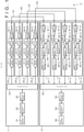
- FIG. 1 shows an example of a configuration of a transmission system according to an embodiment of the invention.
- the transmission system 1 shown includes a transmission side block 11 and a reception side block 12.
- the transmission side block 11 and the reception side block 12 are implemented, for example, by LSIs different from each other or by the same LSI and are provided in the same apparatus wherein information is processed such as a digital camera, a portable telephone set or a personal computer.
- the transmission side block 11 and the reception side block 12 are connected to each other by four transmission lines C1 to C4.
- the transmission lines C1 to C4 may be wire transmission lines or wireless transmission lines. Further, the number of transmission lines between the transmission side block 11 and the reception side block 12 may be five or more.
- the transmission side block 11 includes a signal processing section 21, a rearrangement processing section 22, an ECC (Error Correcting Code) processing section 23, a division section 24, and transmission processing sections 25-1 to 25-4.
- ECC Error Correcting Code
- the transmission processing section 25-1 includes a framing section 31-1, a modulation section 32-1, a DAC (Digital Analog Converter) 33-1 and a transmission amplifier 34-1
- the transmission processing section 25-2 includes a framing section 31-2, a modulation section 32-2, a DAC 33-2 and a transmission amplifier 34-2
- the transmission processing section 25-3 includes a framing section 31-3, a modulation section 32-3, a DAC 33-3 and a transmission amplifier 34-3
- the transmission processing section 25-4 includes a framing section 31-4, a modulation section 32-4, a DAC 33-4 and a transmission amplifier 34-4.
- the division section 24 is provided at a position lower than the ECC processing section 23. Further, at a position lower than the division section 24, a transmission processing section including a framing section, a modulation section, a DAC and a transmission amplifier is provided corresponding to each of the transmission lines C1 to C4.
- the signal processing section 21 carries out various signal processing and outputs transmission data which are data of a transmission object such as image data, text data and audio data obtained by carrying out the signal processing to the rearrangement processing section 22.
- transmission data are inputted from an external circuit of the transmission side block 11 to the rearrangement processing section 22.
- pixel data which configure an image picked up by an external image pickup device such as, for example, a CMOS (Complementary Metal Oxide Semiconductor) image pickup device may be inputted as transmission data in order one by one pixel data.
- CMOS Complementary Metal Oxide Semiconductor
- the rearrangement processing section 22 acquires the transmission data supplied thereto from the signal processing section 21 and carries out rearrangement of the acquired transmission data. For example, in the case where the transmission data are data whose symbol is configured from a predetermined number of bits such as 12 bits, the rearrangement processing section 22 carries out rearrangement of the data to convert the data into data of a unit of 8 bits.
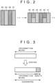
- FIG. 2 illustrates an example of rearrangement of transmission data.
- the rearrangement processing section 22 collects every 8 bits in the inputted order and rearranges the symbols S1 to S4 into symbols s1 to s6 which are data of a unit of 8 bits as indicated ahead of an arrow mark in FIG. 2 .
- the symbol s1 is configured from 8 bits from the first bit to the eighth bit of the symbol S1.
- the symbol s2 is configured from 8 bits including 4 bits from the ninth bit to the 12th bit of the symbol S1 and 4 bits from the first bit to the fourth bit of the symbol S2.
- the symbol s3 is configured from 8 bits from the fifth bit to the 12th bit of the symbol S2.
- the symbol s4 is configured from 8 bits from the first bit to the eighth bit of the symbol S3.
- the symbol s5 is configured from 8 bits including 4 bits from the ninth bit to the 12th bit of the symbol S3 and 4 bits from the first bit to the fourth bit of the symbol S4.
- the symbol s6 is configured from 8 bits from the fifth bit to the 12th bit of the symbol S4.
- the rearrangement processing section 22 carries out a process of rearranging transmission data into data of a unit of 8 bits so that, in whichever bit number each symbol of transmission data is represented, a transmission frame can be produced by the same process by a processing section at a succeeding stage.
- the rearrangement processing section 22 outputs transmission data of a unit of 8 bits obtained by the rearrangement to the ECC processing section 23.
- the ECC processing section 23 calculates an error correction code to be used for error correction of transmission data of a unit of 8 bits supplied thereto from the rearrangement processing section 22 based on the transmission data. Further, the ECC processing section 23 adds a parity which is the error correction code determined by the calculation to the transmission data to carry out error correction coding. For example, the Reed Solomon code is used as the error correction code.
- FIG. 3 illustrates an example of error correction coding by the ECC processing section 23.
- the ECC processing section 23 applies a predetermined number of transmission data of a unit of 8 bits as an information word to a generating polynomial to carry out calculation of a parity. For example, also the parity determined by the ECC processing section 23 is data of a unit of 8 bits. The ECC processing section 23 adds the parity determined by the calculation to the information word as indicated ahead of a solid-white arrow mark to produce a codeword. The ECC processing section 23 outputs the coded data which are the data of the produced codeword in a unit of 8 bits to the division section 24.
- the division section 24 allocates the coded data of a unit of 8 bits supplied thereto from the ECC processing section 23 successively to the transmission lines C1 to C4 beginning with the top data to carry out transmission line division.
- the division section 24 carries out the transmission line division such that, when certain coded data is allocated to the transmission line C4, succeeding coded data are successively allocated to the transmission lines beginning with the transmission line C1.
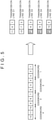
- FIG. 4 illustrates an example of transmission line division.
- each of blocks denoted by numerals represents transmission data or a parity of a unit of 8 bits.
- One codeword is configured from data of 24 bits of the blocks 1 to 3, blocks 4 to 6, blocks 7 to 9 and blocks 10 to 12, and the coded data of the blocks 1 to 12 are supplied in order.
- the division section 24 allocates the coded data supplied thereto from the ECC processing section 23 in the supplied order to the transmission lines C1 to C4 such that those coded data which configure the same codeword may not be transmitted using the same transmission line.
- the coded data of the blocks 1, 2 and 3 which configure the codeword 1 are allocated to the transmission lines C1, C2 and C3, respectively, and the coded data of the blocks 4, 5 and 6 which configure the codeword 2 are allocated to the transmission lines C4, C1 and C2, respectively.
- coded data of the blocks 7, 8 and 9 which configure the codeword 3 are allocated to the transmission lines C3, C4 and C1, respectively, and the coded data of the blocks 10, 11 and 12 which configure the codeword 4 are allocated to the transmission lines C2, C3, and C4, respectively.
- the coded data of the blocks 1, 5 and 9 allocated to the transmission line C1 are supplied in this order to the framing section 31-1, and the coded data of the blocks 2, 6 and 10 allocated to the transmission line C2 are supplied in this order to the framing section 31-2. Further, the coded data of the blocks 3, 7 and 11 allocated to the transmission line C3 are supplied in this order to the framing section 31-3, and the coded data of the blocks 4, 8 and 12 allocated to the transmission line C4 are supplied in this order to the framing section 31-4.
- FIG. 5 illustrates another example of transmission line division.
- the division section 24 allocates coded data supplied from the ECC processing section 23 in the supplied order to the transmission lines C1 to C5 such that those coded data which configure the same codeword may not be transmitted using the same transmission line similarly.
- coded data of the blocks 1, 2 and 3 which configure the codeword 1 are allocated to the transmission lines C1, C2 and C3, respectively, and coded data of the blocks 4, 5 and 6 which configure the codeword 2 are allocated to the transmission lines C4, C5 and C1, respectively.
- coded data of the blocks 7, 8 and 9 which configure the codeword 3 are allocated to the transmission lines C2, C3 and C4, respectively, and coded data of the blocks 10, 11 and 12 which configure the codeword 4 are allocated to the transmission lines C5, C1 and C2, respectively
- the division section 24 allocates padding data to each of those transmission lines to which a smaller amount of coded data is allocated so that the data amounts of the coded data allocated to all transmission lines may be equal to each other. Also the padding data is 8-bit data and has a predetermined value such as "00000000.”
- one padding data is applied to the transmission lines C3, C4 and C5 to which a smaller amount of coded data is allocated.
- a block indicated by slanting lines represents padding data.
- the coded data of the blocks 1, 6 and 11 allocated to the transmission line C1 are supplied in this order to the framing section 31-1, and the coded data of the blocks 2, 7 and 12 allocated to the transmission line C2 are supplied in this order to the framing section 31-2.
- the coded data of the blocks 3 and 8 allocated to the transmission line C3 and the padding data P1 allocated to the transmission line C3 next to the coded data of the block 8 are supplied in this order to the framing section 31-3.
- the coded data of the blocks 4 and 9 allocated to the transmission line C4 and the padding data P2 allocated to the transmission line C4 next to the coded data of the block 9 are supplied in this order to the framing section 31-4.
- the coded data of the blocks 5 and 10 allocated to the transmission line C5 and the padding data P3 allocated to the transmission line C5 next to the coded data of the block 10 are supplied in this order to a transmission processing section not shown which carries out processing of data transmitted thereto from the transmission line C5.
- the padding data is applied by the division section 24.
- the number or bit number of all padding data to be allocated is equal to a number obtained by subtracting the remainder when the number of coded data is divided by the number of transmission lines from the number of transmission lines. Since the sizes of data allocated to the transmission lines are made equal to each other in this manner, it is possible to establish synchronism among processes to be carried out in parallel by the transmission processing sections 25-1 to 25-4.
- the framing section 31-1 of the transmission section 25-1 produces a packet by placing coded data supplied thereto from the division section 24 into the payload and adding a header and a footer regarding transmission data to the payload.
- the framing section 31-1 also places the padding data into the payload similarly to the coded data.
- the framing section 31-1 adds a start code representative of a start position of packet data to the top of the packet and adds an end code representative of an end position of the packet data to the tail end of the packet to produce a transmission frame.
- FIG. 6 illustrates a frame configuration of a transmission frame.
- a header and a footer are added to a payload, in which coded data are placed, to configure one packet. Further, a start code and an end code are added to the packet to configure a transmission frame.
- the framing section 31-1 outputs the frame data, which are data of a transmission frame having such a frame configuration as illustrated in FIG. 6 , to the modulation section 32-1 in order beginning with the top data.
- the modulation section 32-1 modulates the frame data supplied thereto from the framing section 31-1 in accordance with a predetermined method and outputs the frame data after the modulation to the DAC 33-1.
- the DAC 33-1 carries out D/A conversion for the frame data supplied thereto from the modulation section 32-1 and outputs an analog signal obtained by the D/A conversion to the transmission amplifier 34-1.
- the transmission amplifier 34-1 adjusts the signal voltage of the signal supplied thereto from the DAC 33-1 and transmits the signal after the adjustment to the reception side block 12 through the transmission line C1.
- the transmission processing section 25-2 carries out framing, modulation and D/A conversion for coded data allocated to the transmission line C2 and transmits a signal representative of frame data through the transmission line C2.
- the transmission processing section 25-3 carries out framing, modulation and D/A conversion for coded data allocated to the transmission line C3 and transmits a signal representative of frame data through the transmission line C3.
- the transmission processing section 25-4 carries out framing, modulation and D/A conversion for coded data allocated to the transmission line C4 and transmits a signal representative of frame data through the transmission line C4.
- the reception side block 12 includes reception processing sections 51-1 to 51-4, a coupling section 52, an ECC processing section 53, a rearrangement processing section 54 and a signal processing section 55.
- the reception processing section 51-1 includes a reception amplifier 61-1, a clock reproduction section 62-1, an ADC (Analog Digital Converter) 63-1, a demodulation section 64-1 and a frame synchronization section 65-1.
- the reception processing section 51-2 includes a reception amplifier 61-2, a clock reproduction section 62-2, an ADC 63-2, a demodulation section 64-2 and a frame synchronization section 65-2.
- the reception processing section 51-3 includes a reception amplifier 61-3, a clock reproduction section 62-3, an ADC 63-3, a demodulation section 64-3 and a frame synchronization section 65-3.
- the reception processing section 51-4 includes a reception amplifier 61-4, a clock reproduction section 62-4, an ADC 63-4, a demodulation section 64-4 and a frame synchronization section 65-4.
- a signal transmitted from the transmission amplifier 34-1 of the transmission side block 11 is inputted to the reception amplifier 61-1, and a signal transmitted from the transmission amplifier 34-2 is inputted to the reception amplifier 61-2.
- a signal transmitted from the transmission amplifier 34-3 is inputted to the reception amplifier 61-3, and a signal transmitted from the transmission amplifier 34-4 is inputted to the reception amplifier 61-4.
- the coupling section 52 is provided at a position lower than the ECC processing section 53 in the reception side block 12. Further, a reception processing section having a reception amplifier, a clock reproduction section, an ADC, a demodulation section and a frame synchronization section is provided in a corresponding relationship to each of the transmission lines C1 to C4 at a position lower than the coupling section 52.
- the reception amplifier 61-1 of the reception processing section 51-1 receives a signal transmitted thereto from the transmission side block 11, adjusts the signal voltage of the received signal and outputs the signal of the adjusted signal voltage.
- the signal outputted from the reception amplifier 61-1 is inputted to the clock reproduction section 62-1 and the ADC 63-1.
- the clock reproduction section 62-1 detects an edge of the input signal to establish bit synchronism and reproduces a clock signal based on a detection period of the edge.
- the clock reproduction section 62-1 outputs the reproduced clock signal to the ADC 63-1.
- the ADC 63-1 carries out sampling of the input signal in accordance with the clock signal reproduced by the clock reproduction section 62-1 and outputs frame data obtained by the sampling to the demodulation section 64-1.
- the demodulation section 64-1 carries out demodulation of the frame data by a method corresponding to the modulation method used by the modulation section 32-1 of the transmission side block 11 and outputs the frame data after the demodulation to the frame synchronization section 65-1.
- the frame synchronization section 65-1 detects a start code and an end code from the frame data supplied thereto from the demodulation section 64-1 to establish frame synchronism.
- the frame synchronization section 65-1 detects data from the start code to the end code as packet data and outputs coded data placed in the payload of the packet data to the coupling section 52.
- reception processing sections 51-2 to 51-4 carry out similar processes to those carried out by the components of the reception processing section 51-1.
- the reception processing section 51-2 carries out sampling of a signal transmitted thereto through the transmission line C2, demodulation of frame data obtained by the sampling and frame synchronization and outputs coded data to the coupling section 52.
- the reception processing section 51-3 carries out sampling of a signal transmitted thereto through the transmission line C3, demodulation of frame data obtained by the sampling and frame synchronization and outputs coded data to the coupling section 52.
- the reception processing section 51-4 carries out sampling of a signal transmitted thereto through the transmission line C4, demodulation of frame data obtained by the sampling and frame synchronization and outputs coded data to the coupling section 52.
- the coupling section 52 rearranges the coded data supplied thereto from the reception processing sections 51-1 to 51-4 in an order reverse to the allocation order of the coded data to the transmission lines by the division section 24 of the transmission side block 11 to carry out transmission line coupling or integration.
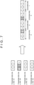
- FIG. 7 illustrates an example of transmission line coupling.
- transmission line division of coded data of the blocks 1 to 12 is carried out in such a manner as described hereinabove with reference to FIG. 4 .
- the coupling section 52 rearranges the coded data in the reverse order to the allocation order of the coded data to the transmission line upon transmission line division to produce coded data of a sequence same as that in the output order of the coded data from the ECC processing section 23 as indicated ahead of a solid-white arrow mark in FIG. 7 .
- the coupling section 52 successively outputs the coded data of the blocks 1 to 12, which configure each codeword produced by carrying out the rearrangement, to the ECC processing section 53.
- the coupling section 52 removes the padding data and outputs only the coded data.
- the ECC processing section 53 carries out error correction arithmetic operation based on the parity included in the coded data supplied thereto from the coupling section 52 to detect an error of the transmission data and carries out correction of the detected error.
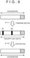
- FIG. 8 illustrates an example of error correction decoding by the ECC processing section 53.
- bits E1 and E2 in the reception data of FIG. 8 are error bits.
- the ECC processing section 53 carries out error detection arithmetic operation based on the parity to detect the bits E1 and E2 and corrects the bits E1 and E2 as indicated ahead of a solid-white arrow mark #12.
- the ECC processing section 53 carries out error correction decoding for each codeword and outputs the transmission data after the error correction to the rearrangement processing section 54.
- the rearrangement processing section 54 rearranges the transmission data of a unit of 8 bits supplied thereto from the ECC processing section 53 in the reverse order to the rearrangement order by the rearrangement processing section 22 of the transmission side block 11.
- the rearrangement processing section 54 carries out reverse processing to the processing described hereinabove with reference to FIG. 2 to convert the transmission data of a unit of 8 bits into transmission data of a unit of a predetermined bit number such as 12 bits.
- the rearrangement processing section 54 outputs the transmission data obtained by the rearrangement to the signal processing section 55.
- the signal processing section 55 uses the transmission data supplied thereto from the rearrangement processing section 54 to carry out various processes. For example, if the transmission data are pixel data which configure an image, then the signal processing section 55 produces an image of one frame based on the pixel data and carries out various processes such as compression of the image data, display of an image and recording of the image data into a recording medium.
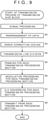
- the signal processing section 21 carries out signal processing and outputs transmission data obtained by the signal processing.
- the rearrangement processing section 22 acquires the transmission data supplied thereto from the signal processing section 21 and carries out rearrangement of the data in such a manner as described hereinabove with reference to FIG. 2 .
- the ECC processing section 23 calculates a parity based on the transmission data of a unit of 8 bits obtained by the rearrangement and adds the parity to the transmission data to carry out error correction coding.
- the division section 24 carries out transmission line division of the coded data obtained by the error correction coding.
- the processes at steps S5 to S8 are repeated in parallel by the transmission processing sections 25-1 to 25-4.
- the framing sections 31-1 to 31-4 individually place the coded data obtained by the error correction coding into the payload and add a header and a footer to produce a packet. Further, the framing sections 31-1 to 31-4 add a start code to the top of the packet and adds an end code to the tail end of the packet to carry out framing of the packet.
- the modulation sections 32-1 to 32-4 individually carry out a modulation process for frame data which configure the transmission frames obtained by the framing.
- the DACs 33-1 to 33-4 carry out D/A conversion for the frame data obtained by the modulation process.
- the transmission amplifiers 34-1 to 34-4 individually transmit the signals obtained by the D/A conversion to the reception side block 12.
- the processes at steps S2 to S8 are carried out repetitively for all transmission data outputted from the signal processing section 21 and end when the processes for all transmission data end.
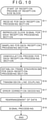
- reception process of the reception side block 12 is described with reference to a flow chart of FIG. 10 .
- Processes at steps S11 to S15 are carried out in parallel by the reception processing sections 51-1 to 51-4.
- the reception amplifiers 61-1 to 61-4 individually receive signals transmitted thereto from the transmission side block 11 and adjust the signal voltage of the received signals.
- the clock reproduction sections 62-1 to 62-4 individually detect an edge of the signals supplied thereto from the reception amplifiers 61-1 to 61-4, respectively, to reproduce a clock signal.
- the ADCs 63-1 to 63-4 carry out sampling in accordance with the clock signals reproduced by the clock reproduction sections 62-1 to 62-4, respectively.
- the demodulation sections 64-1 to 64-4 carry out a demodulation process for frame data obtained by the sampling.
- the frame synchronization sections 65-1 to 65-4 detect a start code and an end code from the frame data supplied thereto from the demodulation sections 64-1 to 64-4, respectively, to establish frame synchronism.
- the frame synchronization sections 65-1 to 65-4 output coded data placed in the payload to the coupling section 52.
- the coupling section 52 rearranges the coded data supplied thereto from the frame synchronization sections 65-1 to 65-4 in the reverse order to the allocation order of the coded data to the transmission lines upon transmission line division to carry out a transmission line coupling.
- the ECC processing section 53 carries out error correction decoding based on the parity included in the codeword configured from the coded data to correct an error of the transmission data.
- the rearrangement processing section 54 carries out rearrangement of the transmission data after the error correction to produce transmission data of a unit of a predetermined number of bits same as that of the data outputted from the signal processing section 21 in the transmission side block 11.
- the processes at steps S11 to S18 are carried out repetitively until the processing for the signals transmitted from the transmission side block 11 is ended.
- the signal processing section 55 carries out signal processing based on the transmission data supplied thereto from the rearrangement processing section 54 at step S19.
- the signal processing section 55 ends the processing.
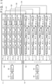
- FIG. 11 A configuration of the transmission side block 11 which carries out error correction coding after transmission line division and a configuration of the reception side block 12 which carries out error correction decoding before transmission line coupling are shown in FIG. 11 .
- a number of ECC processing sections 23-1 to 23-4 equal to the number of transmission lines are provided at a position lower than the division section 24.
- a number of ECC processing sections 53-1 to 53-4 equal to the number of transmission lines are provided at a position lower than the coupling section 52.
- each block indicated by slanting lines represents a block of coded data which suffer from an error
- each block indicated by no slanting line represents a block of coded data which does not suffer from an error.
- the coded data of the block 6 and the coded data of the block 10 transmitted through the transmission line C2 are dispersed into different codewords as indicated ahead of a solid-white arrow mark in FIG. 7 .
- most of error correction codes are vulnerable to burst errors.
- the error correction capacity can be enhanced.
- FIG. 12 shows an example of a hardware configuration of a computer which executes the series of processes described hereinabove in accordance with a program.
- a central processing unit (CPU) 101, a read only memory (ROM) 102 and a random access memory (RAM) 103 are connected to one another by a bus 104.
- CPU central processing unit
- ROM read only memory
- RAM random access memory
- an input/output interface 105 is connected to the bus 104.
- An inputting section 106 including a keyboard, a mouse and so forth, and an outputting section 107 including a display unit, a speaker and so forth are connected to the input/output interface 105.
- a storage section 108 formed from a hard disk, a nonvolatile memory, or the like, a communication section 109 formed from a network interface or the like, and a drive 110 for driving a removable medium 111 are connected to the input/output interface 105.
- the CPU 101 loads a program stored, for example, in the storage section 108 into the RAM 103 through the input/output interface 105 and the bus 104 and executes the program to carry out the series of processes described above.
- the program to be executed by the CPU 101 can be recorded on, for example, a removable medium 111 or can be provided through a wire or wireless transmission medium such as a local area network, the Internet or a digital broadcast, and installed into the storage section 108.
- the program to be executed by the computer may be of the type by which the processes are carried out in a time series in the order as described in the present specification or of the type by which the processes are executed in parallel or executed individually at necessary timings such as when the process is called.
- the present disclosure contains subject matter related to that disclosed in Japanese Priority Patent Application JP 2010-258570 filed in the Japan Patent Office on November 19, 2010 .
Landscapes
- Engineering & Computer Science (AREA)
- Computer Networks & Wireless Communication (AREA)
- Signal Processing (AREA)
- Power Engineering (AREA)
- Detection And Prevention Of Errors In Transmission (AREA)
- Error Detection And Correction (AREA)
Applications Claiming Priority (2)
| Application Number | Priority Date | Filing Date | Title |
|---|---|---|---|
| JP2010258570A JP5761551B2 (ja) | 2010-11-19 | 2010-11-19 | 送信装置、送信方法、受信装置、受信方法、プログラム、および伝送システム |
| EP11187641.3A EP2456112B1 (en) | 2010-11-19 | 2011-11-03 | Error correction methods and apparatus |
Related Parent Applications (2)
| Application Number | Title | Priority Date | Filing Date |
|---|---|---|---|
| EP11187641.3A Division-Into EP2456112B1 (en) | 2010-11-19 | 2011-11-03 | Error correction methods and apparatus |
| EP11187641.3A Division EP2456112B1 (en) | 2010-11-19 | 2011-11-03 | Error correction methods and apparatus |
Publications (2)
| Publication Number | Publication Date |
|---|---|
| EP3451564A1 EP3451564A1 (en) | 2019-03-06 |
| EP3451564B1 true EP3451564B1 (en) | 2022-03-23 |
Family
ID=44992611
Family Applications (2)
| Application Number | Title | Priority Date | Filing Date |
|---|---|---|---|
| EP18195190.6A Active EP3451564B1 (en) | 2010-11-19 | 2011-11-03 | Error correction methods and apparatus |
| EP11187641.3A Active EP2456112B1 (en) | 2010-11-19 | 2011-11-03 | Error correction methods and apparatus |
Family Applications After (1)
| Application Number | Title | Priority Date | Filing Date |
|---|---|---|---|
| EP11187641.3A Active EP2456112B1 (en) | 2010-11-19 | 2011-11-03 | Error correction methods and apparatus |
Country Status (4)
| Country | Link |
|---|---|
| US (1) | US8583985B2 (enExample) |
| EP (2) | EP3451564B1 (enExample) |
| JP (1) | JP5761551B2 (enExample) |
| CN (2) | CN102480340B (enExample) |
Families Citing this family (5)
| Publication number | Priority date | Publication date | Assignee | Title |
|---|---|---|---|---|
| JP5761551B2 (ja) * | 2010-11-19 | 2015-08-12 | ソニー株式会社 | 送信装置、送信方法、受信装置、受信方法、プログラム、および伝送システム |
| WO2013005766A1 (ja) * | 2011-07-04 | 2013-01-10 | 日本電信電話株式会社 | 伝送システム及び伝送方法 |
| JP2013187606A (ja) | 2012-03-06 | 2013-09-19 | Sony Corp | 撮像装置および画像伝送方法 |
| JP2020167634A (ja) * | 2019-03-29 | 2020-10-08 | ソニーセミコンダクタソリューションズ株式会社 | 送信装置、受信装置、及び伝送システム |
| JP2024098810A (ja) * | 2023-01-11 | 2024-07-24 | 国立研究開発法人情報通信研究機構 | 通信ネットワークの制御装置 |
Family Cites Families (13)
| Publication number | Priority date | Publication date | Assignee | Title |
|---|---|---|---|---|
| US3311878A (en) * | 1963-02-14 | 1967-03-28 | Ibm | Error checking system for binary parallel communications |
| JPH05304515A (ja) * | 1992-04-24 | 1993-11-16 | Rohm Co Ltd | デジタルデータ伝送方式 |
| JP3577717B2 (ja) * | 2001-05-18 | 2004-10-13 | 日本電気株式会社 | 通信装置、スクランブラ回路とデスクランブラ回路、そのスクランブル方法とデスクランブル方法 |
| JP3663151B2 (ja) * | 2001-06-07 | 2005-06-22 | 日本電信電話株式会社 | データ転送方法、データ転送システム、および受信装置 |
| JP3877576B2 (ja) * | 2001-11-07 | 2007-02-07 | 沖電気工業株式会社 | 並列送信装置及び並列伝送システム |
| JP2004088246A (ja) * | 2002-08-23 | 2004-03-18 | Toyota Industries Corp | 無線通信方法および無線通信装置 |
| US7978734B2 (en) * | 2004-03-18 | 2011-07-12 | Xocyst Transfer Ag L.L.C. | Multichannel MAC data stream for wireless communication |
| JP2008523660A (ja) * | 2004-12-06 | 2008-07-03 | トムソン ライセンシング | 増分順方向誤り訂正機構用の多重フロー |
| JP2008200344A (ja) * | 2007-02-21 | 2008-09-04 | Hoya Corp | 電子内視鏡および内視鏡プロセッサ |
| JP4774391B2 (ja) * | 2007-08-24 | 2011-09-14 | 株式会社日立製作所 | 光伝送システムおよび信号速度変換装置 |
| WO2009147735A1 (ja) * | 2008-06-04 | 2009-12-10 | 富士通株式会社 | 情報処理装置、データ送信装置およびデータ送信装置のデータ転送方法 |
| JP5388671B2 (ja) | 2009-04-22 | 2014-01-15 | キヤノン株式会社 | 撮像装置及び画像変換方法 |
| JP5761551B2 (ja) * | 2010-11-19 | 2015-08-12 | ソニー株式会社 | 送信装置、送信方法、受信装置、受信方法、プログラム、および伝送システム |
-
2010
- 2010-11-19 JP JP2010258570A patent/JP5761551B2/ja not_active Expired - Fee Related
-
2011
- 2011-10-05 US US13/253,464 patent/US8583985B2/en active Active
- 2011-11-03 EP EP18195190.6A patent/EP3451564B1/en active Active
- 2011-11-03 EP EP11187641.3A patent/EP2456112B1/en active Active
- 2011-11-15 CN CN201110361134.2A patent/CN102480340B/zh not_active Expired - Fee Related
- 2011-11-15 CN CN2011204516069U patent/CN202737883U/zh not_active Expired - Lifetime
Non-Patent Citations (1)
| Title |
|---|
| None * |
Also Published As
| Publication number | Publication date |
|---|---|
| US20120131412A1 (en) | 2012-05-24 |
| EP2456112B1 (en) | 2019-01-02 |
| US8583985B2 (en) | 2013-11-12 |
| EP3451564A1 (en) | 2019-03-06 |
| CN202737883U (zh) | 2013-02-13 |
| CN102480340A (zh) | 2012-05-30 |
| CN102480340B (zh) | 2017-09-01 |
| EP2456112A3 (en) | 2015-03-04 |
| EP2456112A2 (en) | 2012-05-23 |
| JP5761551B2 (ja) | 2015-08-12 |
| JP2012109890A (ja) | 2012-06-07 |
Similar Documents
| Publication | Publication Date | Title |
|---|---|---|
| US10362220B2 (en) | Conversation of pixel data into compression format of pixels | |
| CN102130742B (zh) | 纠错编码装置和方法、及纠错解码装置和方法 | |
| CN1323505C (zh) | 传输线路编码方法、传输线路解码方法及其设备 | |
| US20070202843A1 (en) | Method and system for data partitioning and encoding for transmission of uncompressed video over wireless communication channels | |
| EP3451564B1 (en) | Error correction methods and apparatus | |
| CN202663412U (zh) | 发送设备、接收设备、以及传输系统 | |
| WO2002073812A1 (en) | Error correction encoding method, error correction decoding method, error correction encoding apparatus, and error correction decoding apparatus | |
| JP2009524335A (ja) | 非圧縮avデータを送受信する装置および方法 | |
| CN101444101A (zh) | 使用多个并行编码器的用于数字通信的系统和方法 | |
| US8812938B2 (en) | Coding apparatus, coding method, decoding apparatus, decoding method, program and transmission system | |
| US9667757B2 (en) | Transmitting apparatus, receiving apparatus, and data processing method thereof | |
| KR101367216B1 (ko) | 디지털 방송 수신기 및 그 스트림 처리 방법 | |
| US11930296B2 (en) | Transmission device, reception device, and transmission system with padding code insertion | |
| US20220385959A1 (en) | Transmission device, reception device, and transmission system | |
| JP2003264532A (ja) | 伝送装置及び伝送方法 | |
| KR100740226B1 (ko) | 듀얼 전송 스트림 생성 장치 및 그 방법 | |
| JP3880585B2 (ja) | 誤り訂正復号化装置、誤り訂正復号化方法、誤り訂正符号化・復号化システム、および、誤り訂正符号化・復号化方法 | |
| US20070195822A1 (en) | Method and system for locating packet boundaries | |
| US20120044419A1 (en) | Apparatus and method for transmitting/receiving broadcast data in digital broadcasting system | |
| JPH06261024A (ja) | 信号伝送方法、エンコード装置、信号送信装置、デコード装置及び信号受信装置 | |
| US20220166598A1 (en) | Transmission apparatus, reception apparatus, and transmission system | |
| JPWO2015162738A1 (ja) | 通信装置、通信システムおよび誤り訂正フレーム生成方法 | |
| KR20070109760A (ko) | 비압축 aⅴ 데이터 송수신 방법 및 장치 | |
| KR20100007468A (ko) | 채널 디코딩시 에러 처리 방법 및 장치 |
Legal Events
| Date | Code | Title | Description |
|---|---|---|---|
| PUAI | Public reference made under article 153(3) epc to a published international application that has entered the european phase |
Free format text: ORIGINAL CODE: 0009012 |
|
| STAA | Information on the status of an ep patent application or granted ep patent |
Free format text: STATUS: REQUEST FOR EXAMINATION WAS MADE |
|
| 17P | Request for examination filed |
Effective date: 20181018 |
|
| AC | Divisional application: reference to earlier application |
Ref document number: 2456112 Country of ref document: EP Kind code of ref document: P |
|
| AK | Designated contracting states |
Kind code of ref document: A1 Designated state(s): AL AT BE BG CH CY CZ DE DK EE ES FI FR GB GR HR HU IE IS IT LI LT LU LV MC MK MT NL NO PL PT RO RS SE SI SK SM TR |
|
| STAA | Information on the status of an ep patent application or granted ep patent |
Free format text: STATUS: EXAMINATION IS IN PROGRESS |
|
| 17Q | First examination report despatched |
Effective date: 20201012 |
|
| GRAP | Despatch of communication of intention to grant a patent |
Free format text: ORIGINAL CODE: EPIDOSNIGR1 |
|
| STAA | Information on the status of an ep patent application or granted ep patent |
Free format text: STATUS: GRANT OF PATENT IS INTENDED |
|
| INTG | Intention to grant announced |
Effective date: 20210604 |
|
| RAP3 | Party data changed (applicant data changed or rights of an application transferred) |
Owner name: SONY GROUP CORPORATION |
|
| GRAJ | Information related to disapproval of communication of intention to grant by the applicant or resumption of examination proceedings by the epo deleted |
Free format text: ORIGINAL CODE: EPIDOSDIGR1 |
|
| STAA | Information on the status of an ep patent application or granted ep patent |
Free format text: STATUS: EXAMINATION IS IN PROGRESS |
|
| GRAP | Despatch of communication of intention to grant a patent |
Free format text: ORIGINAL CODE: EPIDOSNIGR1 |
|
| STAA | Information on the status of an ep patent application or granted ep patent |
Free format text: STATUS: GRANT OF PATENT IS INTENDED |
|
| INTC | Intention to grant announced (deleted) | ||
| INTG | Intention to grant announced |
Effective date: 20211019 |
|
| GRAS | Grant fee paid |
Free format text: ORIGINAL CODE: EPIDOSNIGR3 |
|
| GRAA | (expected) grant |
Free format text: ORIGINAL CODE: 0009210 |
|
| STAA | Information on the status of an ep patent application or granted ep patent |
Free format text: STATUS: THE PATENT HAS BEEN GRANTED |
|
| AC | Divisional application: reference to earlier application |
Ref document number: 2456112 Country of ref document: EP Kind code of ref document: P |
|
| AK | Designated contracting states |
Kind code of ref document: B1 Designated state(s): AL AT BE BG CH CY CZ DE DK EE ES FI FR GB GR HR HU IE IS IT LI LT LU LV MC MK MT NL NO PL PT RO RS SE SI SK SM TR |
|
| REG | Reference to a national code |
Ref country code: GB Ref legal event code: FG4D |
|
| REG | Reference to a national code |
Ref country code: CH Ref legal event code: EP |
|
| REG | Reference to a national code |
Ref country code: DE Ref legal event code: R096 Ref document number: 602011072659 Country of ref document: DE |
|
| REG | Reference to a national code |
Ref country code: IE Ref legal event code: FG4D |
|
| REG | Reference to a national code |
Ref country code: AT Ref legal event code: REF Ref document number: 1478165 Country of ref document: AT Kind code of ref document: T Effective date: 20220415 |
|
| REG | Reference to a national code |
Ref country code: LT Ref legal event code: MG9D |
|
| REG | Reference to a national code |
Ref country code: NL Ref legal event code: MP Effective date: 20220323 |
|
| PG25 | Lapsed in a contracting state [announced via postgrant information from national office to epo] |
Ref country code: SE Free format text: LAPSE BECAUSE OF FAILURE TO SUBMIT A TRANSLATION OF THE DESCRIPTION OR TO PAY THE FEE WITHIN THE PRESCRIBED TIME-LIMIT Effective date: 20220323 Ref country code: RS Free format text: LAPSE BECAUSE OF FAILURE TO SUBMIT A TRANSLATION OF THE DESCRIPTION OR TO PAY THE FEE WITHIN THE PRESCRIBED TIME-LIMIT Effective date: 20220323 Ref country code: NO Free format text: LAPSE BECAUSE OF FAILURE TO SUBMIT A TRANSLATION OF THE DESCRIPTION OR TO PAY THE FEE WITHIN THE PRESCRIBED TIME-LIMIT Effective date: 20220623 Ref country code: LT Free format text: LAPSE BECAUSE OF FAILURE TO SUBMIT A TRANSLATION OF THE DESCRIPTION OR TO PAY THE FEE WITHIN THE PRESCRIBED TIME-LIMIT Effective date: 20220323 Ref country code: HR Free format text: LAPSE BECAUSE OF FAILURE TO SUBMIT A TRANSLATION OF THE DESCRIPTION OR TO PAY THE FEE WITHIN THE PRESCRIBED TIME-LIMIT Effective date: 20220323 Ref country code: BG Free format text: LAPSE BECAUSE OF FAILURE TO SUBMIT A TRANSLATION OF THE DESCRIPTION OR TO PAY THE FEE WITHIN THE PRESCRIBED TIME-LIMIT Effective date: 20220623 |
|
| REG | Reference to a national code |
Ref country code: AT Ref legal event code: MK05 Ref document number: 1478165 Country of ref document: AT Kind code of ref document: T Effective date: 20220323 |
|
| PG25 | Lapsed in a contracting state [announced via postgrant information from national office to epo] |
Ref country code: LV Free format text: LAPSE BECAUSE OF FAILURE TO SUBMIT A TRANSLATION OF THE DESCRIPTION OR TO PAY THE FEE WITHIN THE PRESCRIBED TIME-LIMIT Effective date: 20220323 Ref country code: GR Free format text: LAPSE BECAUSE OF FAILURE TO SUBMIT A TRANSLATION OF THE DESCRIPTION OR TO PAY THE FEE WITHIN THE PRESCRIBED TIME-LIMIT Effective date: 20220624 Ref country code: FI Free format text: LAPSE BECAUSE OF FAILURE TO SUBMIT A TRANSLATION OF THE DESCRIPTION OR TO PAY THE FEE WITHIN THE PRESCRIBED TIME-LIMIT Effective date: 20220323 |
|
| PG25 | Lapsed in a contracting state [announced via postgrant information from national office to epo] |
Ref country code: NL Free format text: LAPSE BECAUSE OF FAILURE TO SUBMIT A TRANSLATION OF THE DESCRIPTION OR TO PAY THE FEE WITHIN THE PRESCRIBED TIME-LIMIT Effective date: 20220323 |
|
| PG25 | Lapsed in a contracting state [announced via postgrant information from national office to epo] |
Ref country code: SM Free format text: LAPSE BECAUSE OF FAILURE TO SUBMIT A TRANSLATION OF THE DESCRIPTION OR TO PAY THE FEE WITHIN THE PRESCRIBED TIME-LIMIT Effective date: 20220323 Ref country code: SK Free format text: LAPSE BECAUSE OF FAILURE TO SUBMIT A TRANSLATION OF THE DESCRIPTION OR TO PAY THE FEE WITHIN THE PRESCRIBED TIME-LIMIT Effective date: 20220323 Ref country code: RO Free format text: LAPSE BECAUSE OF FAILURE TO SUBMIT A TRANSLATION OF THE DESCRIPTION OR TO PAY THE FEE WITHIN THE PRESCRIBED TIME-LIMIT Effective date: 20220323 Ref country code: PT Free format text: LAPSE BECAUSE OF FAILURE TO SUBMIT A TRANSLATION OF THE DESCRIPTION OR TO PAY THE FEE WITHIN THE PRESCRIBED TIME-LIMIT Effective date: 20220725 Ref country code: ES Free format text: LAPSE BECAUSE OF FAILURE TO SUBMIT A TRANSLATION OF THE DESCRIPTION OR TO PAY THE FEE WITHIN THE PRESCRIBED TIME-LIMIT Effective date: 20220323 Ref country code: EE Free format text: LAPSE BECAUSE OF FAILURE TO SUBMIT A TRANSLATION OF THE DESCRIPTION OR TO PAY THE FEE WITHIN THE PRESCRIBED TIME-LIMIT Effective date: 20220323 Ref country code: CZ Free format text: LAPSE BECAUSE OF FAILURE TO SUBMIT A TRANSLATION OF THE DESCRIPTION OR TO PAY THE FEE WITHIN THE PRESCRIBED TIME-LIMIT Effective date: 20220323 Ref country code: AT Free format text: LAPSE BECAUSE OF FAILURE TO SUBMIT A TRANSLATION OF THE DESCRIPTION OR TO PAY THE FEE WITHIN THE PRESCRIBED TIME-LIMIT Effective date: 20220323 |
|
| PG25 | Lapsed in a contracting state [announced via postgrant information from national office to epo] |
Ref country code: PL Free format text: LAPSE BECAUSE OF FAILURE TO SUBMIT A TRANSLATION OF THE DESCRIPTION OR TO PAY THE FEE WITHIN THE PRESCRIBED TIME-LIMIT Effective date: 20220323 Ref country code: IS Free format text: LAPSE BECAUSE OF FAILURE TO SUBMIT A TRANSLATION OF THE DESCRIPTION OR TO PAY THE FEE WITHIN THE PRESCRIBED TIME-LIMIT Effective date: 20220723 Ref country code: AL Free format text: LAPSE BECAUSE OF FAILURE TO SUBMIT A TRANSLATION OF THE DESCRIPTION OR TO PAY THE FEE WITHIN THE PRESCRIBED TIME-LIMIT Effective date: 20220323 |
|
| REG | Reference to a national code |
Ref country code: DE Ref legal event code: R097 Ref document number: 602011072659 Country of ref document: DE |
|
| PLBE | No opposition filed within time limit |
Free format text: ORIGINAL CODE: 0009261 |
|
| STAA | Information on the status of an ep patent application or granted ep patent |
Free format text: STATUS: NO OPPOSITION FILED WITHIN TIME LIMIT |
|
| PG25 | Lapsed in a contracting state [announced via postgrant information from national office to epo] |
Ref country code: DK Free format text: LAPSE BECAUSE OF FAILURE TO SUBMIT A TRANSLATION OF THE DESCRIPTION OR TO PAY THE FEE WITHIN THE PRESCRIBED TIME-LIMIT Effective date: 20220323 |
|
| 26N | No opposition filed |
Effective date: 20230102 |
|
| PG25 | Lapsed in a contracting state [announced via postgrant information from national office to epo] |
Ref country code: SI Free format text: LAPSE BECAUSE OF FAILURE TO SUBMIT A TRANSLATION OF THE DESCRIPTION OR TO PAY THE FEE WITHIN THE PRESCRIBED TIME-LIMIT Effective date: 20220323 |
|
| PG25 | Lapsed in a contracting state [announced via postgrant information from national office to epo] |
Ref country code: MC Free format text: LAPSE BECAUSE OF FAILURE TO SUBMIT A TRANSLATION OF THE DESCRIPTION OR TO PAY THE FEE WITHIN THE PRESCRIBED TIME-LIMIT Effective date: 20220323 |
|
| REG | Reference to a national code |
Ref country code: CH Ref legal event code: PL |
|
| P01 | Opt-out of the competence of the unified patent court (upc) registered |
Effective date: 20230528 |
|
| REG | Reference to a national code |
Ref country code: BE Ref legal event code: MM Effective date: 20221130 |
|
| PG25 | Lapsed in a contracting state [announced via postgrant information from national office to epo] |
Ref country code: LI Free format text: LAPSE BECAUSE OF NON-PAYMENT OF DUE FEES Effective date: 20221130 Ref country code: IT Free format text: LAPSE BECAUSE OF FAILURE TO SUBMIT A TRANSLATION OF THE DESCRIPTION OR TO PAY THE FEE WITHIN THE PRESCRIBED TIME-LIMIT Effective date: 20220323 Ref country code: CH Free format text: LAPSE BECAUSE OF NON-PAYMENT OF DUE FEES Effective date: 20221130 |
|
| PG25 | Lapsed in a contracting state [announced via postgrant information from national office to epo] |
Ref country code: LU Free format text: LAPSE BECAUSE OF NON-PAYMENT OF DUE FEES Effective date: 20221103 |
|
| PG25 | Lapsed in a contracting state [announced via postgrant information from national office to epo] |
Ref country code: IE Free format text: LAPSE BECAUSE OF NON-PAYMENT OF DUE FEES Effective date: 20221103 |
|
| PG25 | Lapsed in a contracting state [announced via postgrant information from national office to epo] |
Ref country code: BE Free format text: LAPSE BECAUSE OF NON-PAYMENT OF DUE FEES Effective date: 20221130 |
|
| PG25 | Lapsed in a contracting state [announced via postgrant information from national office to epo] |
Ref country code: HU Free format text: LAPSE BECAUSE OF FAILURE TO SUBMIT A TRANSLATION OF THE DESCRIPTION OR TO PAY THE FEE WITHIN THE PRESCRIBED TIME-LIMIT; INVALID AB INITIO Effective date: 20111103 |
|
| PG25 | Lapsed in a contracting state [announced via postgrant information from national office to epo] |
Ref country code: CY Free format text: LAPSE BECAUSE OF FAILURE TO SUBMIT A TRANSLATION OF THE DESCRIPTION OR TO PAY THE FEE WITHIN THE PRESCRIBED TIME-LIMIT Effective date: 20220323 |
|
| PG25 | Lapsed in a contracting state [announced via postgrant information from national office to epo] |
Ref country code: MK Free format text: LAPSE BECAUSE OF FAILURE TO SUBMIT A TRANSLATION OF THE DESCRIPTION OR TO PAY THE FEE WITHIN THE PRESCRIBED TIME-LIMIT Effective date: 20220323 |
|
| PG25 | Lapsed in a contracting state [announced via postgrant information from national office to epo] |
Ref country code: MT Free format text: LAPSE BECAUSE OF FAILURE TO SUBMIT A TRANSLATION OF THE DESCRIPTION OR TO PAY THE FEE WITHIN THE PRESCRIBED TIME-LIMIT Effective date: 20220323 |
|
| PGFP | Annual fee paid to national office [announced via postgrant information from national office to epo] |
Ref country code: DE Payment date: 20241022 Year of fee payment: 14 |
|
| PGFP | Annual fee paid to national office [announced via postgrant information from national office to epo] |
Ref country code: GB Payment date: 20241022 Year of fee payment: 14 |
|
| PGFP | Annual fee paid to national office [announced via postgrant information from national office to epo] |
Ref country code: FR Payment date: 20241022 Year of fee payment: 14 |
|
| PG25 | Lapsed in a contracting state [announced via postgrant information from national office to epo] |
Ref country code: TR Free format text: LAPSE BECAUSE OF FAILURE TO SUBMIT A TRANSLATION OF THE DESCRIPTION OR TO PAY THE FEE WITHIN THE PRESCRIBED TIME-LIMIT Effective date: 20220323 |