EP3439018A1 - Substrate transfer apparatus, substrate transfer method and exposure apparatus - Google Patents
Substrate transfer apparatus, substrate transfer method and exposure apparatus Download PDFInfo
- Publication number
- EP3439018A1 EP3439018A1 EP18179277.1A EP18179277A EP3439018A1 EP 3439018 A1 EP3439018 A1 EP 3439018A1 EP 18179277 A EP18179277 A EP 18179277A EP 3439018 A1 EP3439018 A1 EP 3439018A1
- Authority
- EP
- European Patent Office
- Prior art keywords
- reticle
- protective cover
- transfer apparatus
- substrate
- substrate transfer
- Prior art date
- Legal status (The legal status is an assumption and is not a legal conclusion. Google has not performed a legal analysis and makes no representation as to the accuracy of the status listed.)
- Withdrawn
Links
Images





Classifications
-
- B—PERFORMING OPERATIONS; TRANSPORTING
- B25—HAND TOOLS; PORTABLE POWER-DRIVEN TOOLS; MANIPULATORS
- B25J—MANIPULATORS; CHAMBERS PROVIDED WITH MANIPULATION DEVICES
- B25J11/00—Manipulators not otherwise provided for
- B25J11/0095—Manipulators transporting wafers
-
- B—PERFORMING OPERATIONS; TRANSPORTING
- B82—NANOTECHNOLOGY
- B82Y—SPECIFIC USES OR APPLICATIONS OF NANOSTRUCTURES; MEASUREMENT OR ANALYSIS OF NANOSTRUCTURES; MANUFACTURE OR TREATMENT OF NANOSTRUCTURES
- B82Y10/00—Nanotechnology for information processing, storage or transmission, e.g. quantum computing or single electron logic
-
- B—PERFORMING OPERATIONS; TRANSPORTING
- B82—NANOTECHNOLOGY
- B82Y—SPECIFIC USES OR APPLICATIONS OF NANOSTRUCTURES; MEASUREMENT OR ANALYSIS OF NANOSTRUCTURES; MANUFACTURE OR TREATMENT OF NANOSTRUCTURES
- B82Y40/00—Manufacture or treatment of nanostructures
-
- G—PHYSICS
- G03—PHOTOGRAPHY; CINEMATOGRAPHY; ANALOGOUS TECHNIQUES USING WAVES OTHER THAN OPTICAL WAVES; ELECTROGRAPHY; HOLOGRAPHY
- G03F—PHOTOMECHANICAL PRODUCTION OF TEXTURED OR PATTERNED SURFACES, e.g. FOR PRINTING, FOR PROCESSING OF SEMICONDUCTOR DEVICES; MATERIALS THEREFOR; ORIGINALS THEREFOR; APPARATUS SPECIALLY ADAPTED THEREFOR
- G03F1/00—Originals for photomechanical production of textured or patterned surfaces, e.g., masks, photo-masks, reticles; Mask blanks or pellicles therefor; Containers specially adapted therefor; Preparation thereof
- G03F1/22—Masks or mask blanks for imaging by radiation of 100nm or shorter wavelength, e.g. X-ray masks, extreme ultraviolet [EUV] masks; Preparation thereof
- G03F1/24—Reflection masks; Preparation thereof
-
- G—PHYSICS
- G03—PHOTOGRAPHY; CINEMATOGRAPHY; ANALOGOUS TECHNIQUES USING WAVES OTHER THAN OPTICAL WAVES; ELECTROGRAPHY; HOLOGRAPHY
- G03F—PHOTOMECHANICAL PRODUCTION OF TEXTURED OR PATTERNED SURFACES, e.g. FOR PRINTING, FOR PROCESSING OF SEMICONDUCTOR DEVICES; MATERIALS THEREFOR; ORIGINALS THEREFOR; APPARATUS SPECIALLY ADAPTED THEREFOR
- G03F1/00—Originals for photomechanical production of textured or patterned surfaces, e.g., masks, photo-masks, reticles; Mask blanks or pellicles therefor; Containers specially adapted therefor; Preparation thereof
- G03F1/38—Masks having auxiliary features, e.g. special coatings or marks for alignment or testing; Preparation thereof
- G03F1/48—Protective coatings
-
- G—PHYSICS
- G03—PHOTOGRAPHY; CINEMATOGRAPHY; ANALOGOUS TECHNIQUES USING WAVES OTHER THAN OPTICAL WAVES; ELECTROGRAPHY; HOLOGRAPHY
- G03F—PHOTOMECHANICAL PRODUCTION OF TEXTURED OR PATTERNED SURFACES, e.g. FOR PRINTING, FOR PROCESSING OF SEMICONDUCTOR DEVICES; MATERIALS THEREFOR; ORIGINALS THEREFOR; APPARATUS SPECIALLY ADAPTED THEREFOR
- G03F1/00—Originals for photomechanical production of textured or patterned surfaces, e.g., masks, photo-masks, reticles; Mask blanks or pellicles therefor; Containers specially adapted therefor; Preparation thereof
- G03F1/62—Pellicles, e.g. pellicle assemblies, e.g. having membrane on support frame; Preparation thereof
-
- G—PHYSICS
- G03—PHOTOGRAPHY; CINEMATOGRAPHY; ANALOGOUS TECHNIQUES USING WAVES OTHER THAN OPTICAL WAVES; ELECTROGRAPHY; HOLOGRAPHY
- G03F—PHOTOMECHANICAL PRODUCTION OF TEXTURED OR PATTERNED SURFACES, e.g. FOR PRINTING, FOR PROCESSING OF SEMICONDUCTOR DEVICES; MATERIALS THEREFOR; ORIGINALS THEREFOR; APPARATUS SPECIALLY ADAPTED THEREFOR
- G03F1/00—Originals for photomechanical production of textured or patterned surfaces, e.g., masks, photo-masks, reticles; Mask blanks or pellicles therefor; Containers specially adapted therefor; Preparation thereof
- G03F1/66—Containers specially adapted for masks, mask blanks or pellicles; Preparation thereof
-
- G—PHYSICS
- G03—PHOTOGRAPHY; CINEMATOGRAPHY; ANALOGOUS TECHNIQUES USING WAVES OTHER THAN OPTICAL WAVES; ELECTROGRAPHY; HOLOGRAPHY
- G03F—PHOTOMECHANICAL PRODUCTION OF TEXTURED OR PATTERNED SURFACES, e.g. FOR PRINTING, FOR PROCESSING OF SEMICONDUCTOR DEVICES; MATERIALS THEREFOR; ORIGINALS THEREFOR; APPARATUS SPECIALLY ADAPTED THEREFOR
- G03F7/00—Photomechanical, e.g. photolithographic, production of textured or patterned surfaces, e.g. printing surfaces; Materials therefor, e.g. comprising photoresists; Apparatus specially adapted therefor
- G03F7/70—Microphotolithographic exposure; Apparatus therefor
- G03F7/70691—Handling of masks or workpieces
- G03F7/70733—Handling masks and workpieces, e.g. exchange of workpiece or mask, transport of workpiece or mask
-
- G—PHYSICS
- G03—PHOTOGRAPHY; CINEMATOGRAPHY; ANALOGOUS TECHNIQUES USING WAVES OTHER THAN OPTICAL WAVES; ELECTROGRAPHY; HOLOGRAPHY
- G03F—PHOTOMECHANICAL PRODUCTION OF TEXTURED OR PATTERNED SURFACES, e.g. FOR PRINTING, FOR PROCESSING OF SEMICONDUCTOR DEVICES; MATERIALS THEREFOR; ORIGINALS THEREFOR; APPARATUS SPECIALLY ADAPTED THEREFOR
- G03F7/00—Photomechanical, e.g. photolithographic, production of textured or patterned surfaces, e.g. printing surfaces; Materials therefor, e.g. comprising photoresists; Apparatus specially adapted therefor
- G03F7/70—Microphotolithographic exposure; Apparatus therefor
- G03F7/70691—Handling of masks or workpieces
- G03F7/70733—Handling masks and workpieces, e.g. exchange of workpiece or mask, transport of workpiece or mask
- G03F7/70741—Handling masks outside exposure position, e.g. reticle libraries
-
- G—PHYSICS
- G03—PHOTOGRAPHY; CINEMATOGRAPHY; ANALOGOUS TECHNIQUES USING WAVES OTHER THAN OPTICAL WAVES; ELECTROGRAPHY; HOLOGRAPHY
- G03F—PHOTOMECHANICAL PRODUCTION OF TEXTURED OR PATTERNED SURFACES, e.g. FOR PRINTING, FOR PROCESSING OF SEMICONDUCTOR DEVICES; MATERIALS THEREFOR; ORIGINALS THEREFOR; APPARATUS SPECIALLY ADAPTED THEREFOR
- G03F7/00—Photomechanical, e.g. photolithographic, production of textured or patterned surfaces, e.g. printing surfaces; Materials therefor, e.g. comprising photoresists; Apparatus specially adapted therefor
- G03F7/70—Microphotolithographic exposure; Apparatus therefor
- G03F7/70691—Handling of masks or workpieces
- G03F7/70733—Handling masks and workpieces, e.g. exchange of workpiece or mask, transport of workpiece or mask
- G03F7/7075—Handling workpieces outside exposure position, e.g. SMIF box
-
- G—PHYSICS
- G03—PHOTOGRAPHY; CINEMATOGRAPHY; ANALOGOUS TECHNIQUES USING WAVES OTHER THAN OPTICAL WAVES; ELECTROGRAPHY; HOLOGRAPHY
- G03F—PHOTOMECHANICAL PRODUCTION OF TEXTURED OR PATTERNED SURFACES, e.g. FOR PRINTING, FOR PROCESSING OF SEMICONDUCTOR DEVICES; MATERIALS THEREFOR; ORIGINALS THEREFOR; APPARATUS SPECIALLY ADAPTED THEREFOR
- G03F7/00—Photomechanical, e.g. photolithographic, production of textured or patterned surfaces, e.g. printing surfaces; Materials therefor, e.g. comprising photoresists; Apparatus specially adapted therefor
- G03F7/70—Microphotolithographic exposure; Apparatus therefor
- G03F7/708—Construction of apparatus, e.g. environment aspects, hygiene aspects or materials
- G03F7/70908—Hygiene, e.g. preventing apparatus pollution, mitigating effect of pollution or removing pollutants from apparatus
-
- G—PHYSICS
- G03—PHOTOGRAPHY; CINEMATOGRAPHY; ANALOGOUS TECHNIQUES USING WAVES OTHER THAN OPTICAL WAVES; ELECTROGRAPHY; HOLOGRAPHY
- G03F—PHOTOMECHANICAL PRODUCTION OF TEXTURED OR PATTERNED SURFACES, e.g. FOR PRINTING, FOR PROCESSING OF SEMICONDUCTOR DEVICES; MATERIALS THEREFOR; ORIGINALS THEREFOR; APPARATUS SPECIALLY ADAPTED THEREFOR
- G03F7/00—Photomechanical, e.g. photolithographic, production of textured or patterned surfaces, e.g. printing surfaces; Materials therefor, e.g. comprising photoresists; Apparatus specially adapted therefor
- G03F7/70—Microphotolithographic exposure; Apparatus therefor
- G03F7/708—Construction of apparatus, e.g. environment aspects, hygiene aspects or materials
- G03F7/70908—Hygiene, e.g. preventing apparatus pollution, mitigating effect of pollution or removing pollutants from apparatus
- G03F7/70916—Pollution mitigation, i.e. mitigating effect of contamination or debris, e.g. foil traps
-
- G—PHYSICS
- G03—PHOTOGRAPHY; CINEMATOGRAPHY; ANALOGOUS TECHNIQUES USING WAVES OTHER THAN OPTICAL WAVES; ELECTROGRAPHY; HOLOGRAPHY
- G03F—PHOTOMECHANICAL PRODUCTION OF TEXTURED OR PATTERNED SURFACES, e.g. FOR PRINTING, FOR PROCESSING OF SEMICONDUCTOR DEVICES; MATERIALS THEREFOR; ORIGINALS THEREFOR; APPARATUS SPECIALLY ADAPTED THEREFOR
- G03F7/00—Photomechanical, e.g. photolithographic, production of textured or patterned surfaces, e.g. printing surfaces; Materials therefor, e.g. comprising photoresists; Apparatus specially adapted therefor
- G03F7/70—Microphotolithographic exposure; Apparatus therefor
- G03F7/708—Construction of apparatus, e.g. environment aspects, hygiene aspects or materials
- G03F7/70983—Optical system protection, e.g. pellicles or removable covers for protection of mask
-
- H—ELECTRICITY
- H10—SEMICONDUCTOR DEVICES; ELECTRIC SOLID-STATE DEVICES NOT OTHERWISE PROVIDED FOR
- H10P—GENERIC PROCESSES OR APPARATUS FOR THE MANUFACTURE OR TREATMENT OF DEVICES COVERED BY CLASS H10
- H10P72/00—Handling or holding of wafers, substrates or devices during manufacture or treatment thereof
- H10P72/04—Apparatus for manufacture or treatment
- H10P72/0451—Apparatus for manufacturing or treating in a plurality of work-stations
- H10P72/0464—Apparatus for manufacturing or treating in a plurality of work-stations characterised by the construction of the transfer chamber
-
- H—ELECTRICITY
- H10—SEMICONDUCTOR DEVICES; ELECTRIC SOLID-STATE DEVICES NOT OTHERWISE PROVIDED FOR
- H10P—GENERIC PROCESSES OR APPARATUS FOR THE MANUFACTURE OR TREATMENT OF DEVICES COVERED BY CLASS H10
- H10P72/00—Handling or holding of wafers, substrates or devices during manufacture or treatment thereof
- H10P72/04—Apparatus for manufacture or treatment
- H10P72/0451—Apparatus for manufacturing or treating in a plurality of work-stations
- H10P72/0468—Apparatus for manufacturing or treating in a plurality of work-stations comprising a chamber adapted to a particular process
- H10P72/0474—Apparatus for manufacturing or treating in a plurality of work-stations comprising a chamber adapted to a particular process comprising at least one lithography chamber
-
- H—ELECTRICITY
- H10—SEMICONDUCTOR DEVICES; ELECTRIC SOLID-STATE DEVICES NOT OTHERWISE PROVIDED FOR
- H10P—GENERIC PROCESSES OR APPARATUS FOR THE MANUFACTURE OR TREATMENT OF DEVICES COVERED BY CLASS H10
- H10P72/00—Handling or holding of wafers, substrates or devices during manufacture or treatment thereof
- H10P72/30—Handling or holding of wafers, substrates or devices during manufacture or treatment thereof for conveying, e.g. between different workstations
- H10P72/33—Handling or holding of wafers, substrates or devices during manufacture or treatment thereof for conveying, e.g. between different workstations into and out of processing chamber
- H10P72/3302—Mechanical parts of transfer devices
-
- H—ELECTRICITY
- H10—SEMICONDUCTOR DEVICES; ELECTRIC SOLID-STATE DEVICES NOT OTHERWISE PROVIDED FOR
- H10P—GENERIC PROCESSES OR APPARATUS FOR THE MANUFACTURE OR TREATMENT OF DEVICES COVERED BY CLASS H10
- H10P72/00—Handling or holding of wafers, substrates or devices during manufacture or treatment thereof
- H10P72/70—Handling or holding of wafers, substrates or devices during manufacture or treatment thereof for supporting or gripping
- H10P72/76—Handling or holding of wafers, substrates or devices during manufacture or treatment thereof for supporting or gripping using mechanical means, e.g. clamps or pinches
- H10P72/7602—Handling or holding of wafers, substrates or devices during manufacture or treatment thereof for supporting or gripping using mechanical means, e.g. clamps or pinches the wafers being placed on a robot blade or gripped by a gripper for conveyance
Definitions
- the present invention pertains to a substrate transfer apparatus that carries substrates on which patterns are formed to a substrate exposure apparatus equipped with a substrate transfer method and a substrate transfer apparatus.
- reticles also known as masks
- EUVL next-generation lithography
- the object of the present invention is to prevent contamination of the inner surface of the protective cover when a substrate is used.
- a substrate transfer apparatus of the first invention carries substrates on which patterns are formed, the substrate transfer apparatus includes a protective cover that protects the substrate when the substrate is not used, and a cover protection means that covers the inner surface of the protective cover when the substrate is used.
- a substrate transfer apparatus of the second invention is according to the substrate transfer apparatus of the first invention, wherein the cover protection means covers the inner surface of the protective cover when the substrate is used in exposure.
- a substrate transfer apparatus of the third invention is according to the substrate transfer apparatus of the first or the second invention, wherein the protective cover includes a plurality of cover members that cover the substrate and are disposed so as to be attachable and removable, and the cover protective means holds the plurality of cover members in a closed state in a standby position.
- a substrate transfer apparatus of the fourth invention is according to the substrate transfer apparatus of the third invention, wherein the cover protective means, after carrying the substrate along with one part of the plurality of cover members to the substrate exposure position, returns the one part of the cover members to the standby position and bringing the plurality of cover members into a closed state.
- a substrate transfer apparatus of the fifth invention is according to the substrate transfer apparatus of the third or the fourth invention, wherein the closed state of the plurality of cover members is a state in which the plurality of cover members are sealed.
- a substrate transfer apparatus of the sixth invention is according to the substrate transfer apparatus of the first or the second invention, wherein the protective cover includes a cover member that covers the pattern on the substrate and is disposed so as to be attachable and removable, and the cover protective means holds the cover member in a standby position in a state mounted to a dummy member that imitates the shape of the substrate.
- a substrate transfer apparatus of the seventh invention is according to the substrate transfer apparatus of any one of the third to sixth inventions, wherein the standby position is a position that performs the alignment of the substrate.
- a substrate transfer apparatus of the eighth invention is according to the substrate transfer apparatus of any one of the third to sixth inventions, wherein in the standby position, the cover member is removed from the substrate.
- a substrate transfer apparatus of the ninth invention is according to the substrate transfer apparatus of any one of the third to sixth inventions, wherein the standby position is a library part that stores the substrate in an exposure atmosphere.
- a substrate transfer apparatus of the tenth invention is according to the substrate transfer apparatus of any one of the third to ninth inventions, wherein the protective cover is grounded at the standby position.
- a substrate transfer apparatus of the eleventh invention carries substrates on which patterns are formed, the substrate transfer apparatus includes in a state protected by a protective cover when the substrate is not used, and a grounding means that grounds the substrate or the protective cover.
- a substrate transfer apparatus of the twelfth invention is according to the substrate transfer apparatus of the eleventh invention, wherein the grounding means is provided on the setting machine that sets the substrate or the protective cover.
- a substrate transfer apparatus of the thirteenth invention is according to the substrate transfer apparatus of the eleventh or the twelfth invention, wherein the substrate is grounded via the protective cover.
- a substrate transfer method of the fourteenth invention carries substrates on which patterns are formed, the substrate transfer method includes the steps of carrying the substrates in a state protected by a protective cover when the substrate is not used, and holding the protective cover on standby so that the inner surface of the protective cover is covered when the substrate is used.
- a substrate exposure apparatus of the fifteenth invention has the substrate transfer apparatus according any one of the first to thirteenth inventions.
- the inner surface of the protective cover is covered by a cover protection means when the substrate is used. Therefore, when the substrate is used, contamination of the inner surface of the protective cover can be prevented.
- the cover protection means covers the inner surface of the protective cover when the substrate is used in exposure. Therefore, when the substrate is used in exposure, contamination of the inner surface of the protective cover can be prevented.
- the protective cover includes a plurality of cover members disposed so as to cover the substrate and to be attachable and removable, and the cover protection means holds the plurality of cover members in a closed state in a standby position. Therefore, in a standby position, contamination of the inner surface of the protective cover can be prevented.
- the cover protection means after carrying the substrate along with one part of the plurality of cover members to the substrate exposure position, returns the one part of the cover members to the standby position and brings the plurality of cover members into a closed state. Therefore, when carrying the substrate to the substrate exposure position, contamination of the substrate can be prevented. Further, in a standby position, contamination of the inner surface of the protective cover can be prevented.
- the closed state of the plurality of cover members is a state in which the plurality of cover members are sealed. Therefore, contamination of the inner surface of the plurality of cover members can be prevented.
- the protective cover includes a cover member disposed so as to cover the pattern on the substrate and to be attachable and removable, and the cover protection means holds the cover member in a standby position in a state mounted to a dummy member that imitates the shape of the substrate. Therefore, in a standby position, since the inner surface of the cover member is covered with the dummy member, contamination of the inner surface of the cover member can be prevented.
- the standby position is a position that performs alignment of the substrate. Therefore, at the alignment position of the substrate, contamination of the inner surface of the cover member can be prevented.
- the standby position is a position where the cover member is removed from the substrate. Therefore, at the position where the cover member is removed from the substrate, contamination of the inner surface of the cover member can be prevented.
- the standby position is a library part that stores the substrate in an exposure environment. Therefore, at the library part, contamination of the inner surface of the cover member can be prevented.
- the protective cover is grounded at the standby position. Therefore, electrostatic charging of the substrate is prevented, and adhering of the particles to the protective cover can be reduced.
- the grounding means grounds the substrate or the protective cover. Therefore, electrostatic charging of the substrate or the protective cover is prevented, and adhering of the particles to the substrate or the protective cover can be reduced.
- the grounding means is provided on a setting machine that sets the substrate or the protective cover. Therefore, the substrate or the protective cover can be grounded by setting the substrate or the protective cover on the setting machine.
- the substrate is grounded via the protective cover. Therefore, the substrate and the protective cover can be grounded at the same time.
- the protective cover when the substrate is used, the protective cover is held in standby in a state wherein the inner surface of the protective cover is covered. Therefore, contamination of the inner surface of the protective cover can be prevented.
- a substrate transfer apparatus of the present invention since a substrate transfer apparatus of the present invention are used, a product with high yield can be obtained using the substrates with little contamination.
- FIG. 1 shows the first embodiment of the substrate transfer apparatus of the present invention.
- This substrate transfer apparatus is provided adjacent to an exposure chamber 13 wherein reticle stage 11 and the like are disposed.
- a robot chamber 17 is provided wherein a vacuum robot 15 is disposed.
- a vacuum reticle library 19 is provided, and on the other side a clean filter pod opener 21 (hereafter called "CFP opener") is provided.
- Exposure chamber 13, robot chamber 17, vacuum reticle library 19 and CFP opener 21 are in vacuum atmosphere.
- a load-lock chamber 23 is disposed in the position where robot chamber 17 faces exposure chamber 13.
- Load-lock chamber 23 communicates to robot chamber 17 via a second gate valve 25.
- [load-lock chamber 23] communicates to atmospheric air via a first gate valve 27.
- a reticle carrier opener 31 is disposed via a second atmospheric robot 29.
- an atmospheric reticle library 35 is disposed via a first atmospheric robot 33.
- an EUVL reticle 37 used in exposure is placed in a state doubly protected by a reticle carrier 39 and a clean filter pod (hereafter called "CFP") 41.
- CFP 41 has the function of a protective cover protecting reticle 37 in a decompression atmosphere.
- the reticle carrier 39 placed in atmospheric reticle library 35 is transferred by the first atmospheric robot 33 to reticle carrier opener 31. Then, reticle carrier 39 is identified by reticle carrier ID reader 43. At this reticle carrier opener 31 reticle carrier 39 is opened and CFP 41 is exposed. The exposed CFP 41 is heated about 2-3 degrees Celsius by temperature compensation lamp 45. The heated CFP 41 is transferred by a second atmospheric robot 29 onto load-lock chamber 23 wherein only the first gate valve 27 is opened. Note that the steps from reticle carrier opener 31 to load-lock chamber 23 are in a clean environment.
- vacuum reticle library 19 for example around 5 sheets of reticle 37 are stored housed in CFP 41.
- the reticles 37 are held at a specified temperature by a temperature adjustment mechanism (not shown).
- the reticles 37 stored in CFP 41 are identified by reticle ID reader 47.
- the identified reticles 37 are transferred by vacuum robot 15 to CFP opener 21 while housed in CFP 41.
- CFP 41 is opened and reticle 37 exposed.
- CFP 41 transferred to CFP opener 21 is set on CFP stage 49.
- CFP 41 includes upper cover member (upper lid) 51 and lower cover member (lower lid) 53. Then, as shown in FIG. 4 , by lowering CFP stage 49 the exterior of upper cover member 51 is locked by locking member 57 on the upper end of support member 55, exposing reticle 37.
- a reference microscope 59 is disposed for performing prealignment of reticle 37. Then, a prealignment mark 37 a formed on the lower surface of reticle 37 is detected by reference microscope 59 from a perforating hole 49 a formed in CFP stage 49 and a transparent window 53 a established in lower cover member 53 through transparent window 53 a , and prealignment occurs by driving CFP stage 49. At this time, the reticle ID can be confirmed by detecting the reticle ID, such as a bar code, through the transparent window 53 a in lower cover member 53.
- the reticle 37 that has completed prealignment is transferred housed in the lower cover 53 of CFP 41 to reticle stage 11 by transfer arm 61 of vacuum robot 15.
- electrostatic chuck 63 is disposed with adsorption face 63 a facing down. Then, in a state where reticle 37 is crimped to adsorption face 63 a of electrostatic chuck 63 by transfer arm 61 via lower cover member 53, the upper surface of reticle 37 is chucked to adsorption face 63 a by turning on electrostatic chuck 63.
- transfer arm 61 carries lower cover member 53 to CFP opener 21, and lower cover member 53 is set on CFP stage 49, which is in the descended position shown in FIG. 4 . Then, the upper cover member 51 and lower cover member 53 of CFP 41 are adhered by raising CFP stage 49, and the inside of upper cover member 51 and lower cover member 53 is sealed airtight. In this embodiment, the closed CFP 41 is held during exposure inside CFP opener 21 in that state. Note that in other cases it is acceptable to hold the CFP opener 21 and prealignment part at the prealignment part. Also, it is acceptable to transfer these to vacuum reticle library 19 and then hold them.
- reticle 37 is set on lower cover member 53 by turning off electrostatic chuck 63.
- reticle 37 is transferred to CFP opener 21 by transfer arm 61 and lower cover member 53, on which is set reticle 37, is set on CFP stage 49, which is in the descended position as shown in FIG. 4 .
- CFP stage 49 the upper cover member 51 of CFP 41 and lower cover member 53 are sealed (refer to FIG. 3 ) and CFP 41 is sealed airtight while reticle 37 is contained inside CFP 41.
- FIG. 7 shows a second embodiment of the substrate transfer apparatus of the present invention.
- the cover member 65 that is a protective cover is mounted so that it can be attached and removed and so that it covers only pattern 37 b on reticle 37.
- cover member 65 is transferred as mounted to cover member 65 by transfer arm 61 to electrostatic chuck 63 of reticle stage 11, then only reticle 37 is chucked to electrostatic chuck 63.
- cover member 65 which remains on transfer arm 61, is transferred to a standby part by transfer arm 61.
- a standby part as shown in FIG. 7 ( d ), an imitation part 67 that imitates the shape of reticle 37 is disposed, and by mounting cover member 65 to this dummy member 67, the inner surface of cover member 65 is covered and protected by dummy member 67.
- cover member 65 is released from dummy member 67 and transferred to the reticle 37 exchange position by transfer arm 61. Then, after mounting cover 65 to the reticle 37 adhered to electrostatic chuck 63, reticle 37 is removed by turning electrostatic chuck 63 off. The removed reticle 37 is transferred along with cover member 65 by transfer arm 61 to vacuum reticle library 19, for example.
- FIG. 8 shows a third embodiment of the substrate transfer apparatus of the present invention.
- a stage-side conductive layer 69 made of aluminum is formed on the upper surface of CFP stage 49 (setting machine) of CFP opener 21, for example.
- This stage-side conductive layer 69 is grounded via ground wire 71.
- conductive layers 51 b and 53 b are formed on upper cover member 51 and lower cover member 53 of CFP 41 and when upper cover member 51 and lower cover member 53 are closed, they create a configuration where both are electrically connected.
- upper cover member 51 and lower cover member 53 are made of conductive material (for example, aluminum), there is no special need to form a conductive layer.
- CFP 41 on CFP stage 49 it becomes grounded.
- a mechanical means of making a reliable electrical contact for example a conductive needle.
- conductive layer 51 b of CFP 41 upper cover member 51 and conductive layer 37 b of reticle 37 The same applies to conductive layer 51 b of CFP 41 upper cover member 51 and conductive layer 37 b of reticle 37.
- a reticle-side conductive layer 37 b is formed only on the upper surface of reticle 37, but it is also acceptable to form a conductive layer on a side surface or lower surface (surface where circuit pattern is formed). In this case, it is necessary to form the conductive layer so that it does not harm exposure, inspection, or various alignments. Also, stage-side conductive layer 69 was formed on the entire upper surface of CFP stage 49, but it is also acceptable to form only a portion of stage-side conductive layer 69, such that at the least reticle 37 or CFP 41 can be grounded.
- grounding of reticle 37 can be made directly from its upper surface, and it is also possible to ground in the same manner as the above example via cover member 65.
- FIG. 9 shows the patterning of the EUV light lithography system inside the exposure chamber 13 of FIG. 1 .
- EUV light is used as the exposure light.
- EUV light has a wavelength of 0.1 ⁇ 400 nm, and for this embodiment a wavelength of 1 ⁇ 50 nm is preferable.
- the projection image uses an image optics system 101, and a reduction image of the pattern is formed on wafer 103 by reticle 37.
- the pattern exposed onto wafer 103 is determined by the reflecting reticle 37 disposed on the lower side of reticle stage 11 via electrostatic chuck 63.
- This reflecting reticle 37 is loaded in and out by the vacuum robot 15 of the above embodiment (indication of vacuum robot 15 on the drawing is omitted).
- wafer 103 is set on top of wafer stage 105. Typically, exposure is done by step scan.
- EUV light used as the illumination light during exposure has low transparency in atmospheric air; for this reason the light path traveled by EUV light is enclosed by vacuum chamber 106, which maintains a vacuum using an appropriate vacuum pump 107.
- EUV light is generated by a laser plasma X-ray source.
- the laser plasma X-ray source includes laser source 108 (operated as an excitation light source) and xenon gas supply apparatus 109.
- the laser plasma X-ray source is enclosed by vacuum chamber 110.
- the EUV light generated by the laser plasma X-ray source passes through window 111 of vacuum chamber 110.
- Laser source 108 generates laser light having a wavelength below ultraviolet, for example using a YAG laser or excimer laser.
- the laser light from laser source 108 is focused and exposed in a flow of xenon gas ejected from nozzle 112 (supplied from xenon supply apparatus 109).
- xenon gas ejected from nozzle 112 supplied from xenon supply apparatus 109.
- the laser light sufficiently warms the xenon gas, generating plasma.
- EUV light photons are emitted.
- a parabolic mirror 113 is disposed adjacent to the xenon gas ejection part.
- Parabolic mirror 113 forms a condenser optics system and is disposed so that the focus point is adjacent to the position where xenon gas is emitted from nozzle 112.
- EUV light is reflected on the multi-layer film of parabolic mirror 113 and reaches condenser mirror 114 through window 111 of vacuum chamber 11.0.
- Condenser mirror 114 focuses EUV light on reflecting reticle 37 and reflects it. EUV light is reflected by condenser mirror 114 and illuminates a specific portion of reticle 37. That is to say, parabolic mirror 113 and condenser 114 compose the illumination system of this apparatus.
- Reticle 37 has a multilayer film that reflects EUV light and an absorbent pattern layer for forming a pattern. By reflecting EUV light with reticle 37, the EUV light is "patternized.” The "patternized" EUV light reaches wafer 103 through projection system 101.
- the image optics system 101 of this embodiment includes 4 reflective mirrors: concave first mirror 115 a , convex second mirror 115 b , convex third mirror 115 c and concave fourth mirror 115 d.
- a multilayer film that reflects EUV light is provided on each mirror 115 a - 115d.
- the EUV light reflected from reticle 37 is reflected sequentially from first mirror 115 a through to fourth mirror 115 d , forming a reduced (for example, 1/4, 1/5, 1/6) image of the reticle pattern.
- Image optics system 101 is made to be telecentric on the image side (wafer 103 side).
- Reticle 37 is supported on at least the X and Y planes by movable reticle stage 11.
- Wafer 103 is preferably supported in the X, Y and Z directions by movable wafer stage 105.
- EUV light is exposed to a specific region on reticle 37 by illumination system 101, and reticle 37 and wafer 103 are moved relative to image optics system 101 at a specified speed according to the reduction percentage of image optics system 101. In this manner, the reticle pattern is exposed in the specified exposure area (toward the die) on wafer 103.
- partition 116 has an opening 116 a , and EUV light is exposed through it from mirror 5 d to wafer 103.
- the space inside partition 116 is evacuated by vacuum pump 117. In this manner, refuse in the form of gas generated by illuminating the resist is prevented from adhering to mirrors 115 a ⁇ d or to reticle 37. For that reason, deterioration of the optical properties thereof is prevented.
- transfer of reticle 37 is performed by the above substrate transfer apparatus; therefore a high yield product can be obtained using a reticle 37 with little contamination.
- the inner surface of the protective cover is covered by a cover protection means when the substrate is used. Therefore, contamination of the inner surface of the protective cover can be prevented when the substrate is used.
- the protective cover is grounded at the standby position. Therefore, electrostatic charging of the substrate is prevented, and adhering of the particles to the protective cover can be reduced.
- the protective cover when the substrate is used, the protective cover is held in standby in a state wherein the inner surface of the protective cover is covered. Therefore, contamination of the inner surface of the protective cover can be prevented.
Landscapes
- Physics & Mathematics (AREA)
- General Physics & Mathematics (AREA)
- Engineering & Computer Science (AREA)
- Health & Medical Sciences (AREA)
- Epidemiology (AREA)
- Public Health (AREA)
- Chemical & Material Sciences (AREA)
- Nanotechnology (AREA)
- Environmental & Geological Engineering (AREA)
- Atmospheric Sciences (AREA)
- Life Sciences & Earth Sciences (AREA)
- Crystallography & Structural Chemistry (AREA)
- Library & Information Science (AREA)
- Condensed Matter Physics & Semiconductors (AREA)
- Manufacturing & Machinery (AREA)
- Theoretical Computer Science (AREA)
- Mathematical Physics (AREA)
- Mechanical Engineering (AREA)
- Robotics (AREA)
- Exposure And Positioning Against Photoresist Photosensitive Materials (AREA)
- Exposure Of Semiconductors, Excluding Electron Or Ion Beam Exposure (AREA)
- Container, Conveyance, Adherence, Positioning, Of Wafer (AREA)
- Preparing Plates And Mask In Photomechanical Process (AREA)
Abstract
Description
- The present invention pertains to a substrate transfer apparatus that carries substrates on which patterns are formed to a substrate exposure apparatus equipped with a substrate transfer method and a substrate transfer apparatus.
- With reticles (also known as masks) used in next-generation lithography such as EPL and EUVL, a common problem is the weakness that pellicles that prevent the adhering of defect-causing particles onto the reticle pattern face cannot be used.
- As a means to resolve this problem, there is a proposal to attach a protective cover when a reticle is not used and only remove it during exposure.
- For example, refer to
U.S. Pat. No. 6,239,863 . - However, in the above method, there was the problem that the protective cover for the reticle used during exposure is left in a state wherein the inner surface of the protective cover is exposed, and it is easy for particles and the like to become adhered to the inner surface of the protective cover.
- The object of the present invention is to prevent contamination of the inner surface of the protective cover when a substrate is used.
- A substrate transfer apparatus of the first invention carries substrates on which patterns are formed, the substrate transfer apparatus includes a protective cover that protects the substrate when the substrate is not used, and a cover protection means that covers the inner surface of the protective cover when the substrate is used.
- A substrate transfer apparatus of the second invention is according to the substrate transfer apparatus of the first invention, wherein the cover protection means covers the inner surface of the protective cover when the substrate is used in exposure.
- A substrate transfer apparatus of the third invention is according to the substrate transfer apparatus of the first or the second invention, wherein the protective cover includes a plurality of cover members that cover the substrate and are disposed so as to be attachable and removable, and the cover protective means holds the plurality of cover members in a closed state in a standby position.
- A substrate transfer apparatus of the fourth invention is according to the substrate transfer apparatus of the third invention, wherein the cover protective means, after carrying the substrate along with one part of the plurality of cover members to the substrate exposure position, returns the one part of the cover members to the standby position and bringing the plurality of cover members into a closed state.
- A substrate transfer apparatus of the fifth invention is according to the substrate transfer apparatus of the third or the fourth invention, wherein the closed state of the plurality of cover members is a state in which the plurality of cover members are sealed.
- A substrate transfer apparatus of the sixth invention is according to the substrate transfer apparatus of the first or the second invention, wherein the protective cover includes a cover member that covers the pattern on the substrate and is disposed so as to be attachable and removable, and the cover protective means holds the cover member in a standby position in a state mounted to a dummy member that imitates the shape of the substrate.
- A substrate transfer apparatus of the seventh invention is according to the substrate transfer apparatus of any one of the third to sixth inventions, wherein the standby position is a position that performs the alignment of the substrate.
- A substrate transfer apparatus of the eighth invention is according to the substrate transfer apparatus of any one of the third to sixth inventions, wherein in the standby position, the cover member is removed from the substrate.
- A substrate transfer apparatus of the ninth invention is according to the substrate transfer apparatus of any one of the third to sixth inventions, wherein the standby position is a library part that stores the substrate in an exposure atmosphere.
- A substrate transfer apparatus of the tenth invention is according to the substrate transfer apparatus of any one of the third to ninth inventions, wherein the protective cover is grounded at the standby position.
- A substrate transfer apparatus of the eleventh invention carries substrates on which patterns are formed, the substrate transfer apparatus includes in a state protected by a protective cover when the substrate is not used, and a grounding means that grounds the substrate or the protective cover.
- A substrate transfer apparatus of the twelfth invention is according to the substrate transfer apparatus of the eleventh invention, wherein the grounding means is provided on the setting machine that sets the substrate or the protective cover.
- A substrate transfer apparatus of the thirteenth invention is according to the substrate transfer apparatus of the eleventh or the twelfth invention, wherein the substrate is grounded via the protective cover.
- A substrate transfer method of the fourteenth invention carries substrates on which patterns are formed, the substrate transfer method includes the steps of carrying the substrates in a state protected by a protective cover when the substrate is not used, and holding the protective cover on standby so that the inner surface of the protective cover is covered when the substrate is used.
- A substrate exposure apparatus of the fifteenth invention has the substrate transfer apparatus according any one of the first to thirteenth inventions.
- According to one aspect of the substrate transfer apparatus of the present invention, the inner surface of the protective cover is covered by a cover protection means when the substrate is used. Therefore, when the substrate is used, contamination of the inner surface of the protective cover can be prevented.
- According to another aspect of the substrate transfer apparatus of the present invention, the cover protection means covers the inner surface of the protective cover when the substrate is used in exposure. Therefore, when the substrate is used in exposure, contamination of the inner surface of the protective cover can be prevented.
- According to another aspect of the substrate transfer apparatus of the present invention, the protective cover includes a plurality of cover members disposed so as to cover the substrate and to be attachable and removable, and the cover protection means holds the plurality of cover members in a closed state in a standby position. Therefore, in a standby position, contamination of the inner surface of the protective cover can be prevented.
- According to another aspect of the substrate transfer apparatus of the present invention, the cover protection means, after carrying the substrate along with one part of the plurality of cover members to the substrate exposure position, returns the one part of the cover members to the standby position and brings the plurality of cover members into a closed state. Therefore, when carrying the substrate to the substrate exposure position, contamination of the substrate can be prevented. Further, in a standby position, contamination of the inner surface of the protective cover can be prevented.
- According to another aspect of the substrate transfer apparatus of the present invention, the closed state of the plurality of cover members is a state in which the plurality of cover members are sealed. Therefore, contamination of the inner surface of the plurality of cover members can be prevented.
- According to another aspect of the substrate transfer apparatus of the present invention, the protective cover includes a cover member disposed so as to cover the pattern on the substrate and to be attachable and removable, and the cover protection means holds the cover member in a standby position in a state mounted to a dummy member that imitates the shape of the substrate. Therefore, in a standby position, since the inner surface of the cover member is covered with the dummy member, contamination of the inner surface of the cover member can be prevented.
- According to another aspect of the substrate transfer apparatus of the present invention, the standby position is a position that performs alignment of the substrate. Therefore, at the alignment position of the substrate, contamination of the inner surface of the cover member can be prevented.
- According to another aspect of the substrate transfer apparatus of the present invention, the standby position is a position where the cover member is removed from the substrate. Therefore, at the position where the cover member is removed from the substrate, contamination of the inner surface of the cover member can be prevented.
- According to another aspect of the substrate transfer apparatus of the present invention, the standby position is a library part that stores the substrate in an exposure environment. Therefore, at the library part, contamination of the inner surface of the cover member can be prevented.
- According to another aspect of the substrate transfer apparatus of the present invention, the protective cover is grounded at the standby position. Therefore, electrostatic charging of the substrate is prevented, and adhering of the particles to the protective cover can be reduced.
- According to another aspect of the substrate transfer apparatus of the present invention, the grounding means grounds the substrate or the protective cover. Therefore, electrostatic charging of the substrate or the protective cover is prevented, and adhering of the particles to the substrate or the protective cover can be reduced.
- According to another aspect of the substrate transfer apparatus of the present invention, the grounding means is provided on a setting machine that sets the substrate or the protective cover. Therefore, the substrate or the protective cover can be grounded by setting the substrate or the protective cover on the setting machine.
- According to another aspect of the substrate transfer apparatus of the present invention, the substrate is grounded via the protective cover. Therefore, the substrate and the protective cover can be grounded at the same time.
- According to an aspect of the substrate transfer method of the present invention, when the substrate is used, the protective cover is held in standby in a state wherein the inner surface of the protective cover is covered. Therefore, contamination of the inner surface of the protective cover can be prevented.
- According to an aspect of the exposure apparatus of the present invention, since a substrate transfer apparatus of the present invention are used, a product with high yield can be obtained using the substrates with little contamination.
-
-
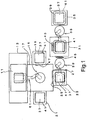
FIG. 1 is an illustration showing a first embodiment of the substrate transfer apparatus of the present invention. -
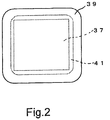
FIG. 2 is an illustration showing a reticle carrier fromFIG. 1 . -
FIG. 3 is an illustration showing the details of a CFP stage fromFIG. 1 . -
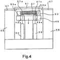
FIG. 4 is an illustration showing the state exposing the reticle from the CFP inFIG. 3 . -
FIG. 5 is an illustration showing a state wherein the reticle is transferred from a CFP stage to a reticle stage ofFIG. 1 . -
FIG. 6 is an illustration showing the state in the CFP stage ofFIG. 1 where the CFP is in standby. -
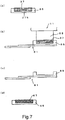
FIG. 7 is an illustration showing a second embodiment of the substrate transfer apparatus of the present invention. -
FIG. 8 is an illustration showing a third embodiment of the substrate transfer apparatus of the present invention. -
FIG. 9 is an illustration showing an embodiment of the exposure apparatus of the present invention. - Below we will explain the details of embodiments of the present invention using drawings. Note that the present invention is not limited to the following embodiments.
-
FIG. 1 shows the first embodiment of the substrate transfer apparatus of the present invention. - This substrate transfer apparatus is provided adjacent to an
exposure chamber 13 whereinreticle stage 11 and the like are disposed. On one side ofreticle chamber 13, arobot chamber 17 is provided wherein a vacuum robot 15 is disposed. On one side ofrobot chamber 17, avacuum reticle library 19 is provided, and on the other side a clean filter pod opener 21 (hereafter called "CFP opener") is provided.Exposure chamber 13,robot chamber 17,vacuum reticle library 19 andCFP opener 21 are in vacuum atmosphere. - In the position where
robot chamber 17 facesexposure chamber 13, a load-lock chamber 23 is disposed. Load-lock chamber 23 communicates torobot chamber 17 via asecond gate valve 25. In addition, [load-lock chamber 23] communicates to atmospheric air via afirst gate valve 27. - On the other side of load-
lock chamber 23, areticle carrier opener 31 is disposed via a secondatmospheric robot 29. On the other side ofreticle carrier opener 31, anatmospheric reticle library 35 is disposed via a firstatmospheric robot 33. - With the above substrate transfer apparatus, in the
atmospheric reticle library 35, as shown inFIG. 2 , anEUVL reticle 37 used in exposure is placed in a state doubly protected by areticle carrier 39 and a clean filter pod (hereafter called "CFP") 41. CFP 41 has the function of a protectivecover protecting reticle 37 in a decompression atmosphere. - The
reticle carrier 39 placed inatmospheric reticle library 35 is transferred by the firstatmospheric robot 33 toreticle carrier opener 31. Then,reticle carrier 39 is identified by reticlecarrier ID reader 43. At thisreticle carrier opener 31reticle carrier 39 is opened and CFP 41 is exposed. The exposed CFP 41 is heated about 2-3 degrees Celsius by temperature compensation lamp 45. The heated CFP 41 is transferred by a secondatmospheric robot 29 onto load-lock chamber 23 wherein only thefirst gate valve 27 is opened. Note that the steps fromreticle carrier opener 31 to load-lock chamber 23 are in a clean environment. - In load-
lock chamber 23, vacuum drawing occurs for each CFP 41 in a state where thefirst gate valve 27 andsecond gate valve 25 are closed. When a specified state of vacuum is achieved in load-lock chamber 23, onlysecond gate valve 25 opens and CFP 41 is transferred tovacuum reticle library 19 by vacuum robot 15. - In
vacuum reticle library 19, for example around 5 sheets ofreticle 37 are stored housed in CFP 41. Thereticles 37 are held at a specified temperature by a temperature adjustment mechanism (not shown). Thereticles 37 stored in CFP 41 are identified byreticle ID reader 47. The identifiedreticles 37 are transferred by vacuum robot 15 toCFP opener 21 while housed in CFP 41. - In
CFP opener 21, CFP 41 is opened andreticle 37 exposed. - In this embodiment, as shown in
FIG. 3 , the CFP 41 transferred toCFP opener 21 is set onCFP stage 49. CFP 41 includes upper cover member (upper lid) 51 and lower cover member (lower lid) 53. Then, as shown inFIG. 4 , by loweringCFP stage 49 the exterior ofupper cover member 51 is locked by lockingmember 57 on the upper end ofsupport member 55, exposingreticle 37. - In this embodiment, at the lower region of
CFP stage 49, areference microscope 59 is disposed for performing prealignment ofreticle 37. Then, a prealignment mark 37a formed on the lower surface ofreticle 37 is detected byreference microscope 59 from a perforating hole 49a formed inCFP stage 49 and a transparent window 53a established inlower cover member 53 through transparent window 53a, and prealignment occurs by drivingCFP stage 49. At this time, the reticle ID can be confirmed by detecting the reticle ID, such as a bar code, through the transparent window 53a inlower cover member 53. - The
reticle 37 that has completed prealignment, as shown inFIG. 5 , is transferred housed in thelower cover 53 of CFP 41 toreticle stage 11 by transfer arm 61 of vacuum robot 15. Inreticle stage 11,electrostatic chuck 63 is disposed with adsorption face 63a facing down. Then, in a state wherereticle 37 is crimped to adsorption face 63a ofelectrostatic chuck 63 by transfer arm 61 vialower cover member 53, the upper surface ofreticle 37 is chucked to adsorption face 63a by turning onelectrostatic chuck 63. - After chucking
reticle 37, transfer arm 61 carrieslower cover member 53 toCFP opener 21, andlower cover member 53 is set onCFP stage 49, which is in the descended position shown inFIG. 4 . Then, theupper cover member 51 andlower cover member 53 of CFP 41 are adhered by raisingCFP stage 49, and the inside ofupper cover member 51 andlower cover member 53 is sealed airtight. In this embodiment, the closed CFP 41 is held during exposure insideCFP opener 21 in that state. Note that in other cases it is acceptable to hold theCFP opener 21 and prealignment part at the prealignment part. Also, it is acceptable to transfer these to vacuumreticle library 19 and then hold them. - When exposure is completed and the exchange of
reticle 37 ofreticle stage 11 occurs, theupper cover member 51 andlower cover member 53 of the CFP 41 held in the state shown inFIG. 6 are separated by loweringCFP stage 49 and lowering the lower cover member 53 (corresponding to the state inFIG. 4 without reticle 37), andlower cover member 53 is transferred to thereticle 37 exchange position by transfer arm 61. - Then, with the
lower cover member 53 in contact withreticle 37, which is attached to electrostatic chuck 63 (refer toFIG. 5 ),reticle 37 is set onlower cover member 53 by turning offelectrostatic chuck 63. In this state,reticle 37 is transferred toCFP opener 21 by transfer arm 61 andlower cover member 53, on which is setreticle 37, is set onCFP stage 49, which is in the descended position as shown inFIG. 4 . Then, by raisingCFP stage 49, theupper cover member 51 of CFP 41 andlower cover member 53 are sealed (refer toFIG. 3 ) and CFP 41 is sealed airtight whilereticle 37 is contained inside CFP 41. - In the above substrate transfer apparatus and method, when
reticle 37 is used in exposure, theupper cover member 51 andlower cover member 53 of CFP 41 are closed and the inner surfaces ofupper cover member 51 andlower cover member 53 are covered; therefore, whenreticle 37 is used in exposure, contamination of the inner surface of CFP 41 can be easily and reliably prevented. Then, because the inner surface of CFP 41 is not contaminated, there is very little contamination ofreticle 37. -
FIG. 7 shows a second embodiment of the substrate transfer apparatus of the present invention. - Note that in this embodiment, the same members as in the first embodiment are assigned the same symbols, so detailed explanation has been omitted.
- In this embodiment, as shown in
FIG. 7 (a), thecover member 65 that is a protective cover is mounted so that it can be attached and removed and so that it covers only pattern 37b onreticle 37. - Then, as shown in
FIG. 7(b) ,cover member 65 is transferred as mounted to covermember 65 by transfer arm 61 toelectrostatic chuck 63 ofreticle stage 11, then only reticle 37 is chucked toelectrostatic chuck 63. - On the other hand, as shown in
FIG. 7(c) cover member 65, which remains on transfer arm 61, is transferred to a standby part by transfer arm 61. In the standby part, as shown inFIG. 7 (d), animitation part 67 that imitates the shape ofreticle 37 is disposed, and by mountingcover member 65 to thisdummy member 67, the inner surface ofcover member 65 is covered and protected bydummy member 67. - Then, when exposure is completed and the exchange of
reticle 37 ofreticle stage 11 occurs,cover member 65 is released fromdummy member 67 and transferred to thereticle 37 exchange position by transfer arm 61. Then, after mountingcover 65 to thereticle 37 adhered toelectrostatic chuck 63,reticle 37 is removed by turningelectrostatic chuck 63 off. The removedreticle 37 is transferred along withcover member 65 by transfer arm 61 tovacuum reticle library 19, for example. - In this embodiment the same result as in the first embodiment can be obtained.
-
FIG. 8 shows a third embodiment of the substrate transfer apparatus of the present invention. - Note that in this embodiment, the same members as in the first embodiment are assigned the same symbols, so detailed explanation has been omitted.
- In this embodiment, a stage-side
conductive layer 69 made of aluminum is formed on the upper surface of CFP stage 49 (setting machine) ofCFP opener 21, for example. This stage-sideconductive layer 69 is grounded via ground wire 71. - On the other hand, on the side surface of
lower cover member 53 of CFP 41, whenlower cover member 53 is set on stage-sideconductive layer 69, a lower cover conductive layer 53b that contacts stage-sideconductive layer 69 is formed. This lower cover conductive layer 53b contacts an upper cover conductive layer 51b formed onupper cover member 51 whenupper cover member 51 is set onlower cover member 53. Also, on the upper surface ofreticle 37, whenupper cover member 51 is set, a reticle conductive layer 37b is formed that contacts upper cover conductive layer 51b. - With this embodiment, the same result as in the first embodiment can be obtained, but in this embodiment, at
CFP stage 49 ,lower cover member 53 of CFP 41,upper cover member 51, orreticle 37 are grounded, therefore electrostatic charging oflower cover member 53,upper cover member 51, orreticle 37 can be easily, reliably prevented. Accordingly, adhesion of particles to these members and the like can be reduced. - Note that in this embodiment, we explained an example where
lower cover member 53,upper cover member 5 1, orreticle 37 are grounded atCFP stage 49; however, it is acceptable for example to ground the plate ofvacuum reticle library 19 on which CFP 41 is set, the setting machine of load-lock chamber 23, or the parts (end effectors) of vacuum robot 15 oratmospheric robot 29 that contact CFP 41. In this case, there is no need to ground at every location; it is acceptable to ground just those locations where one wants to prevent charging of CFP 41 andreticle 37. - Also, in the above embodiment, conductive layers 51b and 53b are formed on
upper cover member 51 andlower cover member 53 of CFP 41 and whenupper cover member 51 andlower cover member 53 are closed, they create a configuration where both are electrically connected. However, ifupper cover member 51 andlower cover member 53 are made of conductive material (for example, aluminum), there is no special need to form a conductive layer. Then, just by placing CFP 41 onCFP stage 49 it becomes grounded. However, in case there is an insufficient electrical contact, it is acceptable to dispose a mechanical means of making a reliable electrical contact (for example a conductive needle). The same applies to conductive layer 51b of CFP 41upper cover member 51 and conductive layer 37b ofreticle 37. - Also, in the above embodiment, a reticle-side conductive layer 37b is formed only on the upper surface of
reticle 37, but it is also acceptable to form a conductive layer on a side surface or lower surface (surface where circuit pattern is formed). In this case, it is necessary to form the conductive layer so that it does not harm exposure, inspection, or various alignments. Also, stage-sideconductive layer 69 was formed on the entire upper surface ofCFP stage 49, but it is also acceptable to form only a portion of stage-sideconductive layer 69, such that at theleast reticle 37 or CFP 41 can be grounded. - Also, as shown in
FIG. 7 , in the case that covermember 65 is established only on the pattern surface 37b ofreticle 37, because the upper surface ofreticle 37 is exposed, grounding ofreticle 37 can be made directly from its upper surface, and it is also possible to ground in the same manner as the above example viacover member 65. -
FIG. 9 shows the patterning of the EUV light lithography system inside theexposure chamber 13 ofFIG. 1 . Note that in this embodiment, the same members as in the first embodiment are assigned the same symbols. In this embodiment, EUV light is used as the exposure light. EUV light has a wavelength of 0.1∼400 nm, and for this embodiment a wavelength of 1∼50 nm is preferable. The projection image uses animage optics system 101, and a reduction image of the pattern is formed onwafer 103 byreticle 37. - The pattern exposed onto
wafer 103 is determined by the reflectingreticle 37 disposed on the lower side ofreticle stage 11 viaelectrostatic chuck 63. This reflectingreticle 37 is loaded in and out by the vacuum robot 15 of the above embodiment (indication of vacuum robot 15 on the drawing is omitted). Also,wafer 103 is set on top ofwafer stage 105. Typically, exposure is done by step scan. - The EUV light used as the illumination light during exposure has low transparency in atmospheric air; for this reason the light path traveled by EUV light is enclosed by
vacuum chamber 106, which maintains a vacuum using anappropriate vacuum pump 107. Also, EUV light is generated by a laser plasma X-ray source. The laser plasma X-ray source includes laser source 108 (operated as an excitation light source) and xenongas supply apparatus 109. The laser plasma X-ray source is enclosed byvacuum chamber 110. The EUV light generated by the laser plasma X-ray source passes throughwindow 111 ofvacuum chamber 110. -
Laser source 108 generates laser light having a wavelength below ultraviolet, for example using a YAG laser or excimer laser. The laser light fromlaser source 108 is focused and exposed in a flow of xenon gas ejected from nozzle 112 (supplied from xenon supply apparatus 109). When laser light is exposed in the xenon flow, the laser light sufficiently warms the xenon gas, generating plasma. When the xenon gas molecules-excited-by the laser fall into a low energy state, EUV light photons are emitted. - A
parabolic mirror 113 is disposed adjacent to the xenon gas ejection part.Parabolic mirror 113 forms a condenser optics system and is disposed so that the focus point is adjacent to the position where xenon gas is emitted fromnozzle 112. EUV light is reflected on the multi-layer film ofparabolic mirror 113 and reachescondenser mirror 114 throughwindow 111 of vacuum chamber 11.0.Condenser mirror 114 focuses EUV light on reflectingreticle 37 and reflects it. EUV light is reflected bycondenser mirror 114 and illuminates a specific portion ofreticle 37. That is to say,parabolic mirror 113 andcondenser 114 compose the illumination system of this apparatus. -
Reticle 37 has a multilayer film that reflects EUV light and an absorbent pattern layer for forming a pattern. By reflecting EUV light withreticle 37, the EUV light is "patternized." The "patternized" EUV light reacheswafer 103 throughprojection system 101. - The
image optics system 101 of this embodiment includes 4 reflective mirrors: concavefirst mirror 115a, convexsecond mirror 115b, convexthird mirror 115 c and concavefourth mirror 115d. A multilayer film that reflects EUV light is provided on eachmirror 115a - 115d. - The EUV light reflected from
reticle 37 is reflected sequentially fromfirst mirror 115a through tofourth mirror 115d, forming a reduced (for example, 1/4, 1/5, 1/6) image of the reticle pattern.Image optics system 101 is made to be telecentric on the image side (wafer 103 side). -
Reticle 37 is supported on at least the X and Y planes bymovable reticle stage 11.Wafer 103 is preferably supported in the X, Y and Z directions bymovable wafer stage 105. When the die onwafer 103 is exposed, EUV light is exposed to a specific region onreticle 37 byillumination system 101, andreticle 37 andwafer 103 are moved relative toimage optics system 101 at a specified speed according to the reduction percentage ofimage optics system 101. In this manner, the reticle pattern is exposed in the specified exposure area (toward the die) onwafer 103. - At time of exposure, it is desirable that
wafer 103 be disposed behind apartition 116 so that the gas that is generated from the resist onwafer 103 not influencemirrors 115a - 115d ofimage optics system 101.Partition 116 has anopening 116a, and EUV light is exposed through it from mirror 5d towafer 103. The space insidepartition 116 is evacuated byvacuum pump 117. In this manner, refuse in the form of gas generated by illuminating the resist is prevented from adhering tomirrors 115a ∼d or toreticle 37. For that reason, deterioration of the optical properties thereof is prevented. - With the exposure apparatus of this embodiment, transfer of
reticle 37 is performed by the above substrate transfer apparatus; therefore a high yield product can be obtained using areticle 37 with little contamination. -
- (1) For the above embodiment, we explained an example where the inner surface of CFP 41 is covered when
reticle 37 is used in exposure, but it is also acceptable for example to cover the inner surface of CFP 41 whenreticle 37 is used in inspection, cleaning, etc. - (2) For the above first embodiment, we explained an example where the protective cover for
reticle 37 is composed on anupper cover member 51 and alower cover member 53, but it is also acceptable for example to be composed of 3 or more members. - (3) For the above embodiment, we explained an example of an exposure apparatus that uses EUV light, but other than this it is also acceptable to broadly apply an exposure apparatus using charged particle rays, i-line, g-line, KrF, ArF, F2 and the like.
- In the above we explained the present invention in detail, however, the invention is not limited to the above embodiments and various modifications may be made without departing from the spirit and scope of the invention. Any improvement may be made in part or all of the components.
- In the substrate transfer apparatus of the present invention, the inner surface of the protective cover is covered by a cover protection means when the substrate is used. Therefore, contamination of the inner surface of the protective cover can be prevented when the substrate is used.
- In the substrate transfer apparatus of the present invention, the protective cover is grounded at the standby position. Therefore, electrostatic charging of the substrate is prevented, and adhering of the particles to the protective cover can be reduced.
- In the substrate transfer method of the present invention, when the substrate is used, the protective cover is held in standby in a state wherein the inner surface of the protective cover is covered. Therefore, contamination of the inner surface of the protective cover can be prevented.
- In the exposure apparatus of the present invention, since a substrate transfer apparatus of the present invention are used, a product with high yield can be obtained using the substrates with little contamination.
- The following numbered paragraphs set out particular combinations of features which are considered relevant to particular embodiments of the present disclosure.
- 1. A substrate transfer apparatus that carries a substrate on which patterns are formed, the substrate transfer apparatus comprising:
- a protective cover that protects the substrate when the substrate is not used, and
- a cover protection means that covers the inner surface of the protective cover when the substrate is used.
- 2. The substrate transfer apparatus according to
paragraph 1, wherein the cover protection means covers the inner surface of the protective cover when the substrate is used in exposure. - 3. The substrate transfer apparatus according to
paragraph 1 or 2, wherein the protective cover comprises a plurality of cover members disposed so as to cover the substrate and to be attachable and removable, and the cover protection means holds the plurality of cover members in a closed state in a standby position. - 4. The substrate transfer apparatus according to
paragraph 3, wherein the cover protection means, after carrying the substrate along with one part of the plurality of cover members to the substrate exposure position, returns the one part of the cover members to the standby position and brings the plurality of cover members into a closed state. - 5. The substrate transfer apparatus according to
paragraph - 6. The substrate transfer apparatus according to
paragraph 1 or 2, wherein the protective cover comprises a cover member disposed so as to cover the patterns on the substrate and to be attachable and removable, and the cover protection means holds the cover member in a standby position in a state mounted to a dummy member that imitates the shape of the substrate. - 7. The substrate transfer apparatus according to any one of
paragraphs 3 to 6, wherein the standby position is a position that performs alignment of the substrate. - 8. The substrate transfer apparatus according to any one of
paragraphs 3 to 6, wherein in the standby position, the cover member is removed from the substrate. - 9. The substrate transfer apparatus according to any one of
paragraphs 3 to 6, wherein the standby position is a library part that stores the substrate in an exposure environment. - 10. The substrate transfer apparatus according to any one of
paragraphs 3 to 9, wherein the protective cover is grounded at the standby position. - 11. A substrate transfer apparatus that carries substrates on which patterns are formed, the substrate transfer apparatus comprising:
- in a state protected by a protective cover that protects the substrate when the substrate is not used, and
- a grounding means that grounds the substrate or the protective cover.
- 12. The substrate transfer apparatus according to
paragraph 11, wherein the grounding means is provided on a setting machine that sets the substrate or the protective cover. - 13. The substrate transfer apparatus according to
paragraph 11 or 12, wherein the substrate is grounded via the protective cover. - 14. A substrate transfer method that carries substrates on which patterns are formed, the substrate transfer method comprising the steps of:
carrying a substrates in a state protected by a protective cover when the substrate is not used, and holding the protective cover on standby so that the inner surface of the protective cover is covered when the substrate is used. - 15. An exposure apparatus having a substrate transfer apparatus according to any one of
paragraphs 1 to 13.
Claims (18)
- A reticle transfer apparatus arranged to carry a reticle on which patterns are formed, the reticle transfer apparatus comprising:a protective cover, that is arranged to protect the reticle when the reticle is present in the protective cover; andcharacterized in that the apparatus is configured to cover an inner surface of the protective cover in a vacuum chamber when the reticle is absent from the protective cover due to the reticle being used in exposure by an EUV light.
- The reticle transfer apparatus according to claim 1, further comprising:means arranged to bring the protective cover to an open state so that the reticle is allowed to be removed from and returned into the protective cover and the means being arranged to bring the protective cover to an closed state,characterized in that the means bring the protective cover to the closed state so that the inner surface of the protective cover is covered when the reticle is absent from the protective cover.
- The reticle transfer apparatus according to claim 2, wherein the protective cover has a plurality of separable protective cover members and the plurality of the protective cover members are separated in the open state.
- The reticle transfer apparatus according to claim 3, wherein the plurality of the separable protective cover members are tightly attached in the closed state.
- The reticle transfer apparatus according to claim 4, wherein the plurality of protective cover members are sealed airtight in the closed state.
- The reticle transfer apparatus according to any one of claims 3 to 5, wherein the means moves one of the plurality of protective cover members.
- The reticle transfer apparatus according to claim 6, wherein the one of the plurality of separable protective cover members is configured to hold the reticle.
- The reticle transfer apparatus according to claim 6 or 7, wherein the means moves the one of the plurality of protective members to remove the reticle from the protective cover and the means returns the one of the plurality of protective members to make the closed state when the reticle is absent from the protective cover.
- The reticle transfer apparatus according to claims 6 to 8, wherein the reticle transfer apparatus is arranged to carry the reticle along with the one of the plurality of protective cover members to a reticle exposure position, and wherein the one of the protective cover members is returned to a position to bring the plurality of protective cover members into the closed state.
- The reticle transfer apparatus according to any one of claims 3-9, wherein alignment of the reticle is performed at which the plurality of protective cover members are separated.
- The reticle transfer apparatus according to any one of claims 2 to 10, wherein the apparatus is provided with a library part that is configured to store the protective cover in the closed state in an exposure environment when the reticle is absent from the protective cover.
- The reticle transfer apparatus according to any one of claims 2 to 11, wherein the protective cover is grounded in the closed state when the reticle is absent from the protective cover.
- The reticle transfer apparatus according to claim 1, wherein the reticle transfer apparatus is configured to mount a dummy member to protect to inner surface of the protective cover when the reticle is removed from the protective cover.
- The reticle transfer apparatus according to claim 13, wherein the dummy member has a shape similar to the reticle.
- The reticle transfer apparatus according to claim 13 or 14, wherein the protective cover has a plurality of separable protective cover members, one of which is configured to hold the reticle, and wherein the dummy member is mounted on the one of the protective cover members when the reticle is absent from the protective cover.
- The reticle transfer apparatus according to claim 15, wherein the one of the protective cover members has the inner surface which faces the pattern surface of the reticle when the reticle held thereon.
- A reticle transfer method for carrying a reticle on which patterns are formed, the reticle transfer method comprising the steps of:removing the reticle from a protective cover that is arranged to protect the reticle when the reticle is present in the protective cover; andcovering an inner surface of the protective cover in a vacuum chamber when the reticle is absent from the protective cover due to the reticle being used in exposure by an EUV light.
- An exposure apparatus having a reticle apparatus according to any one of claims 1 to 16.
Applications Claiming Priority (3)
| Application Number | Priority Date | Filing Date | Title |
|---|---|---|---|
| JP2004310919A JP2006128188A (en) | 2004-10-26 | 2004-10-26 | Substrate transport apparatus, substrate transport method, and exposure apparatus |
| PCT/JP2005/019423 WO2006046488A1 (en) | 2004-10-26 | 2005-10-21 | Substrate transfer apparatus, substrate transfer method and exposure apparatus |
| EP05795225.1A EP1806767B1 (en) | 2004-10-26 | 2005-10-21 | Substrate transfer apparatus, substrate transfer method and exposure apparatus |
Related Parent Applications (1)
| Application Number | Title | Priority Date | Filing Date |
|---|---|---|---|
| EP05795225.1A Division EP1806767B1 (en) | 2004-10-26 | 2005-10-21 | Substrate transfer apparatus, substrate transfer method and exposure apparatus |
Publications (1)
| Publication Number | Publication Date |
|---|---|
| EP3439018A1 true EP3439018A1 (en) | 2019-02-06 |
Family
ID=36205863
Family Applications (2)
| Application Number | Title | Priority Date | Filing Date |
|---|---|---|---|
| EP18179277.1A Withdrawn EP3439018A1 (en) | 2004-10-26 | 2005-10-21 | Substrate transfer apparatus, substrate transfer method and exposure apparatus |
| EP05795225.1A Expired - Lifetime EP1806767B1 (en) | 2004-10-26 | 2005-10-21 | Substrate transfer apparatus, substrate transfer method and exposure apparatus |
Family Applications After (1)
| Application Number | Title | Priority Date | Filing Date |
|---|---|---|---|
| EP05795225.1A Expired - Lifetime EP1806767B1 (en) | 2004-10-26 | 2005-10-21 | Substrate transfer apparatus, substrate transfer method and exposure apparatus |
Country Status (7)
| Country | Link |
|---|---|
| US (2) | US7483123B2 (en) |
| EP (2) | EP3439018A1 (en) |
| JP (1) | JP2006128188A (en) |
| KR (2) | KR101496076B1 (en) |
| CN (1) | CN101006573A (en) |
| TW (1) | TWI383938B (en) |
| WO (1) | WO2006046488A1 (en) |
Families Citing this family (397)
| Publication number | Priority date | Publication date | Assignee | Title |
|---|---|---|---|---|
| US7250114B2 (en) * | 2003-05-30 | 2007-07-31 | Lam Research Corporation | Methods of finishing quartz glass surfaces and components made by the methods |
| TWI447840B (en) * | 2004-11-15 | 2014-08-01 | 尼康股份有限公司 | Substrate transfer device, substrate transfer method, and exposure device |
| US7773198B2 (en) * | 2006-03-28 | 2010-08-10 | Nikon Corporation | Filtered device container assembly with shield for a reticle |
| TWI320059B (en) * | 2006-07-05 | 2010-02-01 | Evaporation equipment and convey device thereof | |
| JPWO2008007521A1 (en) * | 2006-07-11 | 2009-12-10 | 株式会社ニコン | Reticle holding member, reticle stage, exposure apparatus, projection exposure method, and device manufacturing method |
| US20080128303A1 (en) * | 2006-12-05 | 2008-06-05 | Nikon Corporation | Device container assembly with adjustable retainers for a reticle |
| US7960708B2 (en) * | 2007-03-13 | 2011-06-14 | University Of Houston | Device and method for manufacturing a particulate filter with regularly spaced micropores |
| NL1036785A1 (en) | 2008-04-18 | 2009-10-20 | Asml Netherlands Bv | Rapid exchange device for lithography reticles. |
| US10378106B2 (en) | 2008-11-14 | 2019-08-13 | Asm Ip Holding B.V. | Method of forming insulation film by modified PEALD |
| US9394608B2 (en) | 2009-04-06 | 2016-07-19 | Asm America, Inc. | Semiconductor processing reactor and components thereof |
| KR101105416B1 (en) * | 2009-07-23 | 2012-01-17 | 주식회사 디엠에스 | Substrate processing apparatus |
| US8802201B2 (en) | 2009-08-14 | 2014-08-12 | Asm America, Inc. | Systems and methods for thin-film deposition of metal oxides using excited nitrogen-oxygen species |
| JP5358366B2 (en) * | 2009-09-14 | 2013-12-04 | 東京エレクトロン株式会社 | Substrate processing apparatus and method |
| TW201206787A (en) * | 2010-04-30 | 2012-02-16 | Fortrend Engineering Corp | Opener for extreme ultra violet lithography reticle pods |
| US9312155B2 (en) | 2011-06-06 | 2016-04-12 | Asm Japan K.K. | High-throughput semiconductor-processing apparatus equipped with multiple dual-chamber modules |
| JP5772261B2 (en) * | 2011-06-10 | 2015-09-02 | 株式会社ニコン | Mask protection device, transfer device, exposure device, and device manufacturing method |
| US10364496B2 (en) | 2011-06-27 | 2019-07-30 | Asm Ip Holding B.V. | Dual section module having shared and unshared mass flow controllers |
| US10854498B2 (en) | 2011-07-15 | 2020-12-01 | Asm Ip Holding B.V. | Wafer-supporting device and method for producing same |
| US20130023129A1 (en) | 2011-07-20 | 2013-01-24 | Asm America, Inc. | Pressure transmitter for a semiconductor processing environment |
| US8772737B2 (en) * | 2011-09-27 | 2014-07-08 | Applied Materials Israel, Ltd. | Conductive element for electrically coupling an EUVL mask to a supporting chuck |
| US9017481B1 (en) | 2011-10-28 | 2015-04-28 | Asm America, Inc. | Process feed management for semiconductor substrate processing |
| JP5614417B2 (en) * | 2012-01-05 | 2014-10-29 | 株式会社安川電機 | Transport system |
| US9715175B2 (en) | 2012-06-15 | 2017-07-25 | Nikon Corporation | Mask protection device, exposure apparatus, and method for manufacturing device |
| US9558931B2 (en) | 2012-07-27 | 2017-01-31 | Asm Ip Holding B.V. | System and method for gas-phase sulfur passivation of a semiconductor surface |
| US9659799B2 (en) | 2012-08-28 | 2017-05-23 | Asm Ip Holding B.V. | Systems and methods for dynamic semiconductor process scheduling |
| US9021985B2 (en) | 2012-09-12 | 2015-05-05 | Asm Ip Holdings B.V. | Process gas management for an inductively-coupled plasma deposition reactor |
| US10714315B2 (en) | 2012-10-12 | 2020-07-14 | Asm Ip Holdings B.V. | Semiconductor reaction chamber showerhead |
| US20160376700A1 (en) | 2013-02-01 | 2016-12-29 | Asm Ip Holding B.V. | System for treatment of deposition reactor |
| US9589770B2 (en) | 2013-03-08 | 2017-03-07 | Asm Ip Holding B.V. | Method and systems for in-situ formation of intermediate reactive species |
| US9484191B2 (en) | 2013-03-08 | 2016-11-01 | Asm Ip Holding B.V. | Pulsed remote plasma method and system |
| US8993054B2 (en) | 2013-07-12 | 2015-03-31 | Asm Ip Holding B.V. | Method and system to reduce outgassing in a reaction chamber |
| US9240412B2 (en) | 2013-09-27 | 2016-01-19 | Asm Ip Holding B.V. | Semiconductor structure and device and methods of forming same using selective epitaxial process |
| KR101527901B1 (en) * | 2013-10-10 | 2015-06-10 | 피에스케이 주식회사 | Apparatus for treating substrate and method for transfering substrate |
| US9605343B2 (en) | 2013-11-13 | 2017-03-28 | Asm Ip Holding B.V. | Method for forming conformal carbon films, structures conformal carbon film, and system of forming same |
| US10683571B2 (en) | 2014-02-25 | 2020-06-16 | Asm Ip Holding B.V. | Gas supply manifold and method of supplying gases to chamber using same |
| US10167557B2 (en) | 2014-03-18 | 2019-01-01 | Asm Ip Holding B.V. | Gas distribution system, reactor including the system, and methods of using the same |
| US11015245B2 (en) | 2014-03-19 | 2021-05-25 | Asm Ip Holding B.V. | Gas-phase reactor and system having exhaust plenum and components thereof |
| US10858737B2 (en) | 2014-07-28 | 2020-12-08 | Asm Ip Holding B.V. | Showerhead assembly and components thereof |
| US9543180B2 (en) * | 2014-08-01 | 2017-01-10 | Asm Ip Holding B.V. | Apparatus and method for transporting wafers between wafer carrier and process tool under vacuum |
| US9890456B2 (en) | 2014-08-21 | 2018-02-13 | Asm Ip Holding B.V. | Method and system for in situ formation of gas-phase compounds |
| US9657845B2 (en) | 2014-10-07 | 2017-05-23 | Asm Ip Holding B.V. | Variable conductance gas distribution apparatus and method |
| US10941490B2 (en) | 2014-10-07 | 2021-03-09 | Asm Ip Holding B.V. | Multiple temperature range susceptor, assembly, reactor and system including the susceptor, and methods of using the same |
| KR102300403B1 (en) | 2014-11-19 | 2021-09-09 | 에이에스엠 아이피 홀딩 비.브이. | Method of depositing thin film |
| KR102263121B1 (en) | 2014-12-22 | 2021-06-09 | 에이에스엠 아이피 홀딩 비.브이. | Semiconductor device and manufacuring method thereof |
| US10529542B2 (en) | 2015-03-11 | 2020-01-07 | Asm Ip Holdings B.V. | Cross-flow reactor and method |
| US10276355B2 (en) | 2015-03-12 | 2019-04-30 | Asm Ip Holding B.V. | Multi-zone reactor, system including the reactor, and method of using the same |
| US10458018B2 (en) | 2015-06-26 | 2019-10-29 | Asm Ip Holding B.V. | Structures including metal carbide material, devices including the structures, and methods of forming same |
| US10600673B2 (en) | 2015-07-07 | 2020-03-24 | Asm Ip Holding B.V. | Magnetic susceptor to baseplate seal |
| US10043661B2 (en) | 2015-07-13 | 2018-08-07 | Asm Ip Holding B.V. | Method for protecting layer by forming hydrocarbon-based extremely thin film |
| US10083836B2 (en) | 2015-07-24 | 2018-09-25 | Asm Ip Holding B.V. | Formation of boron-doped titanium metal films with high work function |
| US10087525B2 (en) | 2015-08-04 | 2018-10-02 | Asm Ip Holding B.V. | Variable gap hard stop design |
| US9647114B2 (en) | 2015-08-14 | 2017-05-09 | Asm Ip Holding B.V. | Methods of forming highly p-type doped germanium tin films and structures and devices including the films |
| US9960072B2 (en) | 2015-09-29 | 2018-05-01 | Asm Ip Holding B.V. | Variable adjustment for precise matching of multiple chamber cavity housings |
| US10211308B2 (en) | 2015-10-21 | 2019-02-19 | Asm Ip Holding B.V. | NbMC layers |
| US10322384B2 (en) | 2015-11-09 | 2019-06-18 | Asm Ip Holding B.V. | Counter flow mixer for process chamber |
| US9627221B1 (en) | 2015-12-28 | 2017-04-18 | Asm Ip Holding B.V. | Continuous process incorporating atomic layer etching |
| US11139308B2 (en) | 2015-12-29 | 2021-10-05 | Asm Ip Holding B.V. | Atomic layer deposition of III-V compounds to form V-NAND devices |
| US10529554B2 (en) | 2016-02-19 | 2020-01-07 | Asm Ip Holding B.V. | Method for forming silicon nitride film selectively on sidewalls or flat surfaces of trenches |
| US10468251B2 (en) | 2016-02-19 | 2019-11-05 | Asm Ip Holding B.V. | Method for forming spacers using silicon nitride film for spacer-defined multiple patterning |
| US10501866B2 (en) | 2016-03-09 | 2019-12-10 | Asm Ip Holding B.V. | Gas distribution apparatus for improved film uniformity in an epitaxial system |
| US10343920B2 (en) | 2016-03-18 | 2019-07-09 | Asm Ip Holding B.V. | Aligned carbon nanotubes |
| US9892913B2 (en) | 2016-03-24 | 2018-02-13 | Asm Ip Holding B.V. | Radial and thickness control via biased multi-port injection settings |
| US10087522B2 (en) | 2016-04-21 | 2018-10-02 | Asm Ip Holding B.V. | Deposition of metal borides |
| US10190213B2 (en) | 2016-04-21 | 2019-01-29 | Asm Ip Holding B.V. | Deposition of metal borides |
| US10865475B2 (en) | 2016-04-21 | 2020-12-15 | Asm Ip Holding B.V. | Deposition of metal borides and silicides |
| US10367080B2 (en) | 2016-05-02 | 2019-07-30 | Asm Ip Holding B.V. | Method of forming a germanium oxynitride film |
| US10032628B2 (en) | 2016-05-02 | 2018-07-24 | Asm Ip Holding B.V. | Source/drain performance through conformal solid state doping |
| KR102592471B1 (en) | 2016-05-17 | 2023-10-20 | 에이에스엠 아이피 홀딩 비.브이. | Method of forming metal interconnection and method of fabricating semiconductor device using the same |
| US11453943B2 (en) | 2016-05-25 | 2022-09-27 | Asm Ip Holding B.V. | Method for forming carbon-containing silicon/metal oxide or nitride film by ALD using silicon precursor and hydrocarbon precursor |
| US10388509B2 (en) | 2016-06-28 | 2019-08-20 | Asm Ip Holding B.V. | Formation of epitaxial layers via dislocation filtering |
| US10612137B2 (en) | 2016-07-08 | 2020-04-07 | Asm Ip Holdings B.V. | Organic reactants for atomic layer deposition |
| US9859151B1 (en) | 2016-07-08 | 2018-01-02 | Asm Ip Holding B.V. | Selective film deposition method to form air gaps |
| US9793135B1 (en) | 2016-07-14 | 2017-10-17 | ASM IP Holding B.V | Method of cyclic dry etching using etchant film |
| US10714385B2 (en) | 2016-07-19 | 2020-07-14 | Asm Ip Holding B.V. | Selective deposition of tungsten |
| US10381226B2 (en) | 2016-07-27 | 2019-08-13 | Asm Ip Holding B.V. | Method of processing substrate |
| KR102532607B1 (en) | 2016-07-28 | 2023-05-15 | 에이에스엠 아이피 홀딩 비.브이. | Substrate processing apparatus and method of operating the same |
| US10395919B2 (en) | 2016-07-28 | 2019-08-27 | Asm Ip Holding B.V. | Method and apparatus for filling a gap |
| US10177025B2 (en) | 2016-07-28 | 2019-01-08 | Asm Ip Holding B.V. | Method and apparatus for filling a gap |
| US9887082B1 (en) | 2016-07-28 | 2018-02-06 | Asm Ip Holding B.V. | Method and apparatus for filling a gap |
| US9812320B1 (en) | 2016-07-28 | 2017-11-07 | Asm Ip Holding B.V. | Method and apparatus for filling a gap |
| US10090316B2 (en) | 2016-09-01 | 2018-10-02 | Asm Ip Holding B.V. | 3D stacked multilayer semiconductor memory using doped select transistor channel |
| US10410943B2 (en) | 2016-10-13 | 2019-09-10 | Asm Ip Holding B.V. | Method for passivating a surface of a semiconductor and related systems |
| US10643826B2 (en) | 2016-10-26 | 2020-05-05 | Asm Ip Holdings B.V. | Methods for thermally calibrating reaction chambers |
| US11532757B2 (en) | 2016-10-27 | 2022-12-20 | Asm Ip Holding B.V. | Deposition of charge trapping layers |
| US10229833B2 (en) | 2016-11-01 | 2019-03-12 | Asm Ip Holding B.V. | Methods for forming a transition metal nitride film on a substrate by atomic layer deposition and related semiconductor device structures |
| US10435790B2 (en) | 2016-11-01 | 2019-10-08 | Asm Ip Holding B.V. | Method of subatmospheric plasma-enhanced ALD using capacitively coupled electrodes with narrow gap |
| US10643904B2 (en) | 2016-11-01 | 2020-05-05 | Asm Ip Holdings B.V. | Methods for forming a semiconductor device and related semiconductor device structures |
| US10714350B2 (en) | 2016-11-01 | 2020-07-14 | ASM IP Holdings, B.V. | Methods for forming a transition metal niobium nitride film on a substrate by atomic layer deposition and related semiconductor device structures |
| US10134757B2 (en) | 2016-11-07 | 2018-11-20 | Asm Ip Holding B.V. | Method of processing a substrate and a device manufactured by using the method |
| KR102546317B1 (en) | 2016-11-15 | 2023-06-21 | 에이에스엠 아이피 홀딩 비.브이. | Gas supply unit and substrate processing apparatus including the same |
| US10340135B2 (en) | 2016-11-28 | 2019-07-02 | Asm Ip Holding B.V. | Method of topologically restricted plasma-enhanced cyclic deposition of silicon or metal nitride |
| KR102762543B1 (en) | 2016-12-14 | 2025-02-05 | 에이에스엠 아이피 홀딩 비.브이. | Substrate processing apparatus |
| US11581186B2 (en) | 2016-12-15 | 2023-02-14 | Asm Ip Holding B.V. | Sequential infiltration synthesis apparatus |
| US11447861B2 (en) | 2016-12-15 | 2022-09-20 | Asm Ip Holding B.V. | Sequential infiltration synthesis apparatus and a method of forming a patterned structure |
| US9916980B1 (en) | 2016-12-15 | 2018-03-13 | Asm Ip Holding B.V. | Method of forming a structure on a substrate |
| KR102700194B1 (en) | 2016-12-19 | 2024-08-28 | 에이에스엠 아이피 홀딩 비.브이. | Substrate processing apparatus |
| US10269558B2 (en) | 2016-12-22 | 2019-04-23 | Asm Ip Holding B.V. | Method of forming a structure on a substrate |
| US10867788B2 (en) | 2016-12-28 | 2020-12-15 | Asm Ip Holding B.V. | Method of forming a structure on a substrate |
| CN108288597A (en) * | 2017-01-10 | 2018-07-17 | 台湾积体电路制造股份有限公司 | Storage box and particle detection method |
| US11390950B2 (en) | 2017-01-10 | 2022-07-19 | Asm Ip Holding B.V. | Reactor system and method to reduce residue buildup during a film deposition process |
| US10655221B2 (en) | 2017-02-09 | 2020-05-19 | Asm Ip Holding B.V. | Method for depositing oxide film by thermal ALD and PEALD |
| US10468261B2 (en) | 2017-02-15 | 2019-11-05 | Asm Ip Holding B.V. | Methods for forming a metallic film on a substrate by cyclical deposition and related semiconductor device structures |
| US10529563B2 (en) | 2017-03-29 | 2020-01-07 | Asm Ip Holdings B.V. | Method for forming doped metal oxide films on a substrate by cyclical deposition and related semiconductor device structures |
| US10283353B2 (en) | 2017-03-29 | 2019-05-07 | Asm Ip Holding B.V. | Method of reforming insulating film deposited on substrate with recess pattern |
| US10103040B1 (en) | 2017-03-31 | 2018-10-16 | Asm Ip Holding B.V. | Apparatus and method for manufacturing a semiconductor device |
| USD830981S1 (en) | 2017-04-07 | 2018-10-16 | Asm Ip Holding B.V. | Susceptor for semiconductor substrate processing apparatus |
| KR102457289B1 (en) | 2017-04-25 | 2022-10-21 | 에이에스엠 아이피 홀딩 비.브이. | Method for depositing a thin film and manufacturing a semiconductor device |
| US10446393B2 (en) | 2017-05-08 | 2019-10-15 | Asm Ip Holding B.V. | Methods for forming silicon-containing epitaxial layers and related semiconductor device structures |
| US10770286B2 (en) | 2017-05-08 | 2020-09-08 | Asm Ip Holdings B.V. | Methods for selectively forming a silicon nitride film on a substrate and related semiconductor device structures |
| US10892156B2 (en) | 2017-05-08 | 2021-01-12 | Asm Ip Holding B.V. | Methods for forming a silicon nitride film on a substrate and related semiconductor device structures |
| US11360400B2 (en) | 2017-05-19 | 2022-06-14 | Massachusetts Institute Of Technology | Transport system having a magnetically levitated transportation stage |
| US10504742B2 (en) | 2017-05-31 | 2019-12-10 | Asm Ip Holding B.V. | Method of atomic layer etching using hydrogen plasma |
| US10886123B2 (en) | 2017-06-02 | 2021-01-05 | Asm Ip Holding B.V. | Methods for forming low temperature semiconductor layers and related semiconductor device structures |
| US12040200B2 (en) | 2017-06-20 | 2024-07-16 | Asm Ip Holding B.V. | Semiconductor processing apparatus and methods for calibrating a semiconductor processing apparatus |
| US11306395B2 (en) | 2017-06-28 | 2022-04-19 | Asm Ip Holding B.V. | Methods for depositing a transition metal nitride film on a substrate by atomic layer deposition and related deposition apparatus |
| US10685834B2 (en) | 2017-07-05 | 2020-06-16 | Asm Ip Holdings B.V. | Methods for forming a silicon germanium tin layer and related semiconductor device structures |
| KR20190009245A (en) | 2017-07-18 | 2019-01-28 | 에이에스엠 아이피 홀딩 비.브이. | Methods for forming a semiconductor device structure and related semiconductor device structures |
| US11374112B2 (en) | 2017-07-19 | 2022-06-28 | Asm Ip Holding B.V. | Method for depositing a group IV semiconductor and related semiconductor device structures |
| US10541333B2 (en) | 2017-07-19 | 2020-01-21 | Asm Ip Holding B.V. | Method for depositing a group IV semiconductor and related semiconductor device structures |
| US11018002B2 (en) | 2017-07-19 | 2021-05-25 | Asm Ip Holding B.V. | Method for selectively depositing a Group IV semiconductor and related semiconductor device structures |
| US10590535B2 (en) | 2017-07-26 | 2020-03-17 | Asm Ip Holdings B.V. | Chemical treatment, deposition and/or infiltration apparatus and method for using the same |
| US10605530B2 (en) | 2017-07-26 | 2020-03-31 | Asm Ip Holding B.V. | Assembly of a liner and a flange for a vertical furnace as well as the liner and the vertical furnace |
| US10312055B2 (en) | 2017-07-26 | 2019-06-04 | Asm Ip Holding B.V. | Method of depositing film by PEALD using negative bias |
| TWI815813B (en) | 2017-08-04 | 2023-09-21 | 荷蘭商Asm智慧財產控股公司 | Showerhead assembly for distributing a gas within a reaction chamber |
| US10692741B2 (en) | 2017-08-08 | 2020-06-23 | Asm Ip Holdings B.V. | Radiation shield |
| US10770336B2 (en) | 2017-08-08 | 2020-09-08 | Asm Ip Holding B.V. | Substrate lift mechanism and reactor including same |
| US11139191B2 (en) | 2017-08-09 | 2021-10-05 | Asm Ip Holding B.V. | Storage apparatus for storing cassettes for substrates and processing apparatus equipped therewith |
| US10249524B2 (en) | 2017-08-09 | 2019-04-02 | Asm Ip Holding B.V. | Cassette holder assembly for a substrate cassette and holding member for use in such assembly |
| US11769682B2 (en) | 2017-08-09 | 2023-09-26 | Asm Ip Holding B.V. | Storage apparatus for storing cassettes for substrates and processing apparatus equipped therewith |
| US10236177B1 (en) | 2017-08-22 | 2019-03-19 | ASM IP Holding B.V.. | Methods for depositing a doped germanium tin semiconductor and related semiconductor device structures |
| USD900036S1 (en) | 2017-08-24 | 2020-10-27 | Asm Ip Holding B.V. | Heater electrical connector and adapter |
| US11830730B2 (en) | 2017-08-29 | 2023-11-28 | Asm Ip Holding B.V. | Layer forming method and apparatus |
| KR102491945B1 (en) | 2017-08-30 | 2023-01-26 | 에이에스엠 아이피 홀딩 비.브이. | Substrate processing apparatus |
| US11295980B2 (en) | 2017-08-30 | 2022-04-05 | Asm Ip Holding B.V. | Methods for depositing a molybdenum metal film over a dielectric surface of a substrate by a cyclical deposition process and related semiconductor device structures |
| US11056344B2 (en) | 2017-08-30 | 2021-07-06 | Asm Ip Holding B.V. | Layer forming method |
| KR102401446B1 (en) | 2017-08-31 | 2022-05-24 | 에이에스엠 아이피 홀딩 비.브이. | Substrate processing apparatus |
| US10607895B2 (en) | 2017-09-18 | 2020-03-31 | Asm Ip Holdings B.V. | Method for forming a semiconductor device structure comprising a gate fill metal |
| KR102630301B1 (en) | 2017-09-21 | 2024-01-29 | 에이에스엠 아이피 홀딩 비.브이. | Method of sequential infiltration synthesis treatment of infiltrateable material and structures and devices formed using same |
| US10844484B2 (en) | 2017-09-22 | 2020-11-24 | Asm Ip Holding B.V. | Apparatus for dispensing a vapor phase reactant to a reaction chamber and related methods |
| US10658205B2 (en) | 2017-09-28 | 2020-05-19 | Asm Ip Holdings B.V. | Chemical dispensing apparatus and methods for dispensing a chemical to a reaction chamber |
| US10403504B2 (en) | 2017-10-05 | 2019-09-03 | Asm Ip Holding B.V. | Method for selectively depositing a metallic film on a substrate |
| US10319588B2 (en) | 2017-10-10 | 2019-06-11 | Asm Ip Holding B.V. | Method for depositing a metal chalcogenide on a substrate by cyclical deposition |
| US10923344B2 (en) | 2017-10-30 | 2021-02-16 | Asm Ip Holding B.V. | Methods for forming a semiconductor structure and related semiconductor structures |
| KR102443047B1 (en) | 2017-11-16 | 2022-09-14 | 에이에스엠 아이피 홀딩 비.브이. | Substrate processing apparatus method and apparatus manufactured thereby |
| US10910262B2 (en) | 2017-11-16 | 2021-02-02 | Asm Ip Holding B.V. | Method of selectively depositing a capping layer structure on a semiconductor device structure |
| US11022879B2 (en) | 2017-11-24 | 2021-06-01 | Asm Ip Holding B.V. | Method of forming an enhanced unexposed photoresist layer |
| JP7214724B2 (en) | 2017-11-27 | 2023-01-30 | エーエスエム アイピー ホールディング ビー.ブイ. | Storage device for storing wafer cassettes used in batch furnaces |
| TWI791689B (en) | 2017-11-27 | 2023-02-11 | 荷蘭商Asm智慧財產控股私人有限公司 | Apparatus including a clean mini environment |
| US10290508B1 (en) | 2017-12-05 | 2019-05-14 | Asm Ip Holding B.V. | Method for forming vertical spacers for spacer-defined patterning |
| US10872771B2 (en) | 2018-01-16 | 2020-12-22 | Asm Ip Holding B. V. | Method for depositing a material film on a substrate within a reaction chamber by a cyclical deposition process and related device structures |
| TWI799494B (en) | 2018-01-19 | 2023-04-21 | 荷蘭商Asm 智慧財產控股公司 | Deposition method |
| KR102695659B1 (en) | 2018-01-19 | 2024-08-14 | 에이에스엠 아이피 홀딩 비.브이. | Method for depositing a gap filling layer by plasma assisted deposition |
| USD903477S1 (en) | 2018-01-24 | 2020-12-01 | Asm Ip Holdings B.V. | Metal clamp |
| US11018047B2 (en) | 2018-01-25 | 2021-05-25 | Asm Ip Holding B.V. | Hybrid lift pin |
| US10535516B2 (en) | 2018-02-01 | 2020-01-14 | Asm Ip Holdings B.V. | Method for depositing a semiconductor structure on a surface of a substrate and related semiconductor structures |
| USD880437S1 (en) | 2018-02-01 | 2020-04-07 | Asm Ip Holding B.V. | Gas supply plate for semiconductor manufacturing apparatus |
| US11081345B2 (en) | 2018-02-06 | 2021-08-03 | Asm Ip Holding B.V. | Method of post-deposition treatment for silicon oxide film |
| US11685991B2 (en) | 2018-02-14 | 2023-06-27 | Asm Ip Holding B.V. | Method for depositing a ruthenium-containing film on a substrate by a cyclical deposition process |
| US10896820B2 (en) | 2018-02-14 | 2021-01-19 | Asm Ip Holding B.V. | Method for depositing a ruthenium-containing film on a substrate by a cyclical deposition process |
| US10731249B2 (en) | 2018-02-15 | 2020-08-04 | Asm Ip Holding B.V. | Method of forming a transition metal containing film on a substrate by a cyclical deposition process, a method for supplying a transition metal halide compound to a reaction chamber, and related vapor deposition apparatus |
| KR102636427B1 (en) | 2018-02-20 | 2024-02-13 | 에이에스엠 아이피 홀딩 비.브이. | Substrate processing method and apparatus |
| US10658181B2 (en) | 2018-02-20 | 2020-05-19 | Asm Ip Holding B.V. | Method of spacer-defined direct patterning in semiconductor fabrication |
| US10975470B2 (en) | 2018-02-23 | 2021-04-13 | Asm Ip Holding B.V. | Apparatus for detecting or monitoring for a chemical precursor in a high temperature environment |
| US11473195B2 (en) | 2018-03-01 | 2022-10-18 | Asm Ip Holding B.V. | Semiconductor processing apparatus and a method for processing a substrate |
| US11629406B2 (en) | 2018-03-09 | 2023-04-18 | Asm Ip Holding B.V. | Semiconductor processing apparatus comprising one or more pyrometers for measuring a temperature of a substrate during transfer of the substrate |
| US11114283B2 (en) | 2018-03-16 | 2021-09-07 | Asm Ip Holding B.V. | Reactor, system including the reactor, and methods of manufacturing and using same |
| KR102646467B1 (en) | 2018-03-27 | 2024-03-11 | 에이에스엠 아이피 홀딩 비.브이. | Method of forming an electrode on a substrate and a semiconductor device structure including an electrode |
| US11230766B2 (en) | 2018-03-29 | 2022-01-25 | Asm Ip Holding B.V. | Substrate processing apparatus and method |
| US10510536B2 (en) | 2018-03-29 | 2019-12-17 | Asm Ip Holding B.V. | Method of depositing a co-doped polysilicon film on a surface of a substrate within a reaction chamber |
| US11088002B2 (en) | 2018-03-29 | 2021-08-10 | Asm Ip Holding B.V. | Substrate rack and a substrate processing system and method |
| KR102501472B1 (en) | 2018-03-30 | 2023-02-20 | 에이에스엠 아이피 홀딩 비.브이. | Substrate processing method |
| KR102600229B1 (en) | 2018-04-09 | 2023-11-10 | 에이에스엠 아이피 홀딩 비.브이. | Substrate supporting device, substrate processing apparatus including the same and substrate processing method |
| KR102602980B1 (en) | 2018-04-16 | 2023-11-16 | 현대자동차주식회사 | Aluminium alloy for die casting and manufacturing method for aluminium alloy casting using the same |
| TWI843623B (en) | 2018-05-08 | 2024-05-21 | 荷蘭商Asm Ip私人控股有限公司 | Methods for depositing an oxide film on a substrate by a cyclical deposition process and related device structures |
| US12025484B2 (en) | 2018-05-08 | 2024-07-02 | Asm Ip Holding B.V. | Thin film forming method |
| US12272527B2 (en) | 2018-05-09 | 2025-04-08 | Asm Ip Holding B.V. | Apparatus for use with hydrogen radicals and method of using same |
| KR20190129718A (en) | 2018-05-11 | 2019-11-20 | 에이에스엠 아이피 홀딩 비.브이. | Methods for forming a doped metal carbide film on a substrate and related semiconductor device structures |
| KR102596988B1 (en) | 2018-05-28 | 2023-10-31 | 에이에스엠 아이피 홀딩 비.브이. | Method of processing a substrate and a device manufactured by the same |
| TWI840362B (en) | 2018-06-04 | 2024-05-01 | 荷蘭商Asm Ip私人控股有限公司 | Wafer handling chamber with moisture reduction |
| US11718913B2 (en) | 2018-06-04 | 2023-08-08 | Asm Ip Holding B.V. | Gas distribution system and reactor system including same |
| US11286562B2 (en) | 2018-06-08 | 2022-03-29 | Asm Ip Holding B.V. | Gas-phase chemical reactor and method of using same |
| KR102568797B1 (en) | 2018-06-21 | 2023-08-21 | 에이에스엠 아이피 홀딩 비.브이. | Substrate processing system |
| US10797133B2 (en) | 2018-06-21 | 2020-10-06 | Asm Ip Holding B.V. | Method for depositing a phosphorus doped silicon arsenide film and related semiconductor device structures |
| TWI871083B (en) | 2018-06-27 | 2025-01-21 | 荷蘭商Asm Ip私人控股有限公司 | Cyclic deposition processes for forming metal-containing material |
| US11499222B2 (en) | 2018-06-27 | 2022-11-15 | Asm Ip Holding B.V. | Cyclic deposition methods for forming metal-containing material and films and structures including the metal-containing material |
| US10612136B2 (en) | 2018-06-29 | 2020-04-07 | ASM IP Holding, B.V. | Temperature-controlled flange and reactor system including same |
| KR102686758B1 (en) | 2018-06-29 | 2024-07-18 | 에이에스엠 아이피 홀딩 비.브이. | Method for depositing a thin film and manufacturing a semiconductor device |
| US10755922B2 (en) | 2018-07-03 | 2020-08-25 | Asm Ip Holding B.V. | Method for depositing silicon-free carbon-containing film as gap-fill layer by pulse plasma-assisted deposition |
| US10388513B1 (en) | 2018-07-03 | 2019-08-20 | Asm Ip Holding B.V. | Method for depositing silicon-free carbon-containing film as gap-fill layer by pulse plasma-assisted deposition |
| US10767789B2 (en) | 2018-07-16 | 2020-09-08 | Asm Ip Holding B.V. | Diaphragm valves, valve components, and methods for forming valve components |
| US10483099B1 (en) | 2018-07-26 | 2019-11-19 | Asm Ip Holding B.V. | Method for forming thermally stable organosilicon polymer film |
| US11053591B2 (en) | 2018-08-06 | 2021-07-06 | Asm Ip Holding B.V. | Multi-port gas injection system and reactor system including same |
| US10883175B2 (en) | 2018-08-09 | 2021-01-05 | Asm Ip Holding B.V. | Vertical furnace for processing substrates and a liner for use therein |
| US10829852B2 (en) | 2018-08-16 | 2020-11-10 | Asm Ip Holding B.V. | Gas distribution device for a wafer processing apparatus |
| US11430674B2 (en) | 2018-08-22 | 2022-08-30 | Asm Ip Holding B.V. | Sensor array, apparatus for dispensing a vapor phase reactant to a reaction chamber and related methods |
| US11024523B2 (en) | 2018-09-11 | 2021-06-01 | Asm Ip Holding B.V. | Substrate processing apparatus and method |
| KR102707956B1 (en) | 2018-09-11 | 2024-09-19 | 에이에스엠 아이피 홀딩 비.브이. | Method for deposition of a thin film |
| US11049751B2 (en) | 2018-09-14 | 2021-06-29 | Asm Ip Holding B.V. | Cassette supply system to store and handle cassettes and processing apparatus equipped therewith |
| CN110970344B (en) | 2018-10-01 | 2024-10-25 | Asmip控股有限公司 | Substrate holding device, system including the same and method of using the same |
| US11232963B2 (en) | 2018-10-03 | 2022-01-25 | Asm Ip Holding B.V. | Substrate processing apparatus and method |
| KR102592699B1 (en) | 2018-10-08 | 2023-10-23 | 에이에스엠 아이피 홀딩 비.브이. | Substrate support unit and apparatuses for depositing thin film and processing the substrate including the same |
| US10847365B2 (en) | 2018-10-11 | 2020-11-24 | Asm Ip Holding B.V. | Method of forming conformal silicon carbide film by cyclic CVD |
| US10811256B2 (en) | 2018-10-16 | 2020-10-20 | Asm Ip Holding B.V. | Method for etching a carbon-containing feature |
| KR102605121B1 (en) | 2018-10-19 | 2023-11-23 | 에이에스엠 아이피 홀딩 비.브이. | Substrate processing apparatus and substrate processing method |
| KR102546322B1 (en) | 2018-10-19 | 2023-06-21 | 에이에스엠 아이피 홀딩 비.브이. | Substrate processing apparatus and substrate processing method |
| USD948463S1 (en) | 2018-10-24 | 2022-04-12 | Asm Ip Holding B.V. | Susceptor for semiconductor substrate supporting apparatus |
| US10381219B1 (en) | 2018-10-25 | 2019-08-13 | Asm Ip Holding B.V. | Methods for forming a silicon nitride film |
| US12378665B2 (en) | 2018-10-26 | 2025-08-05 | Asm Ip Holding B.V. | High temperature coatings for a preclean and etch apparatus and related methods |
| US11087997B2 (en) | 2018-10-31 | 2021-08-10 | Asm Ip Holding B.V. | Substrate processing apparatus for processing substrates |
| KR102748291B1 (en) | 2018-11-02 | 2024-12-31 | 에이에스엠 아이피 홀딩 비.브이. | Substrate support unit and substrate processing apparatus including the same |
| US11572620B2 (en) | 2018-11-06 | 2023-02-07 | Asm Ip Holding B.V. | Methods for selectively depositing an amorphous silicon film on a substrate |
| US11031242B2 (en) | 2018-11-07 | 2021-06-08 | Asm Ip Holding B.V. | Methods for depositing a boron doped silicon germanium film |
| US10847366B2 (en) | 2018-11-16 | 2020-11-24 | Asm Ip Holding B.V. | Methods for depositing a transition metal chalcogenide film on a substrate by a cyclical deposition process |
| US10818758B2 (en) | 2018-11-16 | 2020-10-27 | Asm Ip Holding B.V. | Methods for forming a metal silicate film on a substrate in a reaction chamber and related semiconductor device structures |
| US10559458B1 (en) | 2018-11-26 | 2020-02-11 | Asm Ip Holding B.V. | Method of forming oxynitride film |
| US12040199B2 (en) | 2018-11-28 | 2024-07-16 | Asm Ip Holding B.V. | Substrate processing apparatus for processing substrates |
| US11217444B2 (en) | 2018-11-30 | 2022-01-04 | Asm Ip Holding B.V. | Method for forming an ultraviolet radiation responsive metal oxide-containing film |
| KR102636428B1 (en) | 2018-12-04 | 2024-02-13 | 에이에스엠 아이피 홀딩 비.브이. | A method for cleaning a substrate processing apparatus |
| US11158513B2 (en) | 2018-12-13 | 2021-10-26 | Asm Ip Holding B.V. | Methods for forming a rhenium-containing film on a substrate by a cyclical deposition process and related semiconductor device structures |
| JP7504584B2 (en) | 2018-12-14 | 2024-06-24 | エーエスエム・アイピー・ホールディング・ベー・フェー | Method and system for forming device structures using selective deposition of gallium nitride - Patents.com |
| TWI866480B (en) | 2019-01-17 | 2024-12-11 | 荷蘭商Asm Ip 私人控股有限公司 | Methods of forming a transition metal containing film on a substrate by a cyclical deposition process |
| KR102727227B1 (en) | 2019-01-22 | 2024-11-07 | 에이에스엠 아이피 홀딩 비.브이. | Semiconductor processing device |
| CN111524788B (en) | 2019-02-01 | 2023-11-24 | Asm Ip私人控股有限公司 | Method for forming topologically selective films of silicon oxide |
| KR20200102357A (en) | 2019-02-20 | 2020-08-31 | 에이에스엠 아이피 홀딩 비.브이. | Apparatus and methods for plug fill deposition in 3-d nand applications |
| TWI873122B (en) | 2019-02-20 | 2025-02-21 | 荷蘭商Asm Ip私人控股有限公司 | Method of filling a recess formed within a surface of a substrate, semiconductor structure formed according to the method, and semiconductor processing apparatus |
| KR102626263B1 (en) | 2019-02-20 | 2024-01-16 | 에이에스엠 아이피 홀딩 비.브이. | Cyclical deposition method including treatment step and apparatus for same |
| TWI845607B (en) | 2019-02-20 | 2024-06-21 | 荷蘭商Asm Ip私人控股有限公司 | Cyclical deposition method and apparatus for filling a recess formed within a substrate surface |
| TWI842826B (en) | 2019-02-22 | 2024-05-21 | 荷蘭商Asm Ip私人控股有限公司 | Substrate processing apparatus and method for processing substrate |
| KR102782593B1 (en) | 2019-03-08 | 2025-03-14 | 에이에스엠 아이피 홀딩 비.브이. | Structure Including SiOC Layer and Method of Forming Same |
| KR102762833B1 (en) | 2019-03-08 | 2025-02-04 | 에이에스엠 아이피 홀딩 비.브이. | STRUCTURE INCLUDING SiOCN LAYER AND METHOD OF FORMING SAME |
| KR102858005B1 (en) | 2019-03-08 | 2025-09-09 | 에이에스엠 아이피 홀딩 비.브이. | Method for Selective Deposition of Silicon Nitride Layer and Structure Including Selectively-Deposited Silicon Nitride Layer |
| JP2020167398A (en) | 2019-03-28 | 2020-10-08 | エーエスエム・アイピー・ホールディング・ベー・フェー | Door openers and substrate processing equipment provided with door openers |
| KR102809999B1 (en) | 2019-04-01 | 2025-05-19 | 에이에스엠 아이피 홀딩 비.브이. | Method of manufacturing semiconductor device |
| KR102897355B1 (en) | 2019-04-19 | 2025-12-08 | 에이에스엠 아이피 홀딩 비.브이. | Layer forming method and apparatus |
| KR20200125453A (en) | 2019-04-24 | 2020-11-04 | 에이에스엠 아이피 홀딩 비.브이. | Gas-phase reactor system and method of using same |
| KR102869364B1 (en) | 2019-05-07 | 2025-10-10 | 에이에스엠 아이피 홀딩 비.브이. | Method for Reforming Amorphous Carbon Polymer Film |
| KR102929471B1 (en) | 2019-05-07 | 2026-02-20 | 에이에스엠 아이피 홀딩 비.브이. | Chemical source vessel with dip tube |
| KR102929472B1 (en) | 2019-05-10 | 2026-02-20 | 에이에스엠 아이피 홀딩 비.브이. | Method of depositing material onto a surface and structure formed according to the method |
| JP7612342B2 (en) | 2019-05-16 | 2025-01-14 | エーエスエム・アイピー・ホールディング・ベー・フェー | Wafer boat handling apparatus, vertical batch furnace and method |
| JP7598201B2 (en) | 2019-05-16 | 2024-12-11 | エーエスエム・アイピー・ホールディング・ベー・フェー | Wafer boat handling apparatus, vertical batch furnace and method |
| USD975665S1 (en) | 2019-05-17 | 2023-01-17 | Asm Ip Holding B.V. | Susceptor shaft |
| USD947913S1 (en) | 2019-05-17 | 2022-04-05 | Asm Ip Holding B.V. | Susceptor shaft |
| USD935572S1 (en) | 2019-05-24 | 2021-11-09 | Asm Ip Holding B.V. | Gas channel plate |
| USD922229S1 (en) | 2019-06-05 | 2021-06-15 | Asm Ip Holding B.V. | Device for controlling a temperature of a gas supply unit |
| KR20200141002A (en) | 2019-06-06 | 2020-12-17 | 에이에스엠 아이피 홀딩 비.브이. | Method of using a gas-phase reactor system including analyzing exhausted gas |
| KR102918757B1 (en) | 2019-06-10 | 2026-01-28 | 에이에스엠 아이피 홀딩 비.브이. | Method for cleaning quartz epitaxial chambers |
| KR20200143254A (en) | 2019-06-11 | 2020-12-23 | 에이에스엠 아이피 홀딩 비.브이. | Method of forming an electronic structure using an reforming gas, system for performing the method, and structure formed using the method |
| USD944946S1 (en) | 2019-06-14 | 2022-03-01 | Asm Ip Holding B.V. | Shower plate |
| USD931978S1 (en) | 2019-06-27 | 2021-09-28 | Asm Ip Holding B.V. | Showerhead vacuum transport |
| KR102911421B1 (en) | 2019-07-03 | 2026-01-12 | 에이에스엠 아이피 홀딩 비.브이. | Temperature control assembly for substrate processing apparatus and method of using same |
| JP7499079B2 (en) | 2019-07-09 | 2024-06-13 | エーエスエム・アイピー・ホールディング・ベー・フェー | Plasma device using coaxial waveguide and substrate processing method |
| CN112216646B (en) | 2019-07-10 | 2026-02-10 | Asmip私人控股有限公司 | Substrate support assembly and substrate processing apparatus including the thereof |
| KR102895115B1 (en) | 2019-07-16 | 2025-12-03 | 에이에스엠 아이피 홀딩 비.브이. | Substrate processing apparatus |
| KR102860110B1 (en) | 2019-07-17 | 2025-09-16 | 에이에스엠 아이피 홀딩 비.브이. | Methods of forming silicon germanium structures |
| TWI826704B (en) | 2019-07-17 | 2023-12-21 | 荷蘭商Asm Ip私人控股有限公司 | Radical assist ignition plasma system and method |
| US11643724B2 (en) | 2019-07-18 | 2023-05-09 | Asm Ip Holding B.V. | Method of forming structures using a neutral beam |
| TWI839544B (en) | 2019-07-19 | 2024-04-21 | 荷蘭商Asm Ip私人控股有限公司 | Method of forming topology-controlled amorphous carbon polymer film |
| KR102903090B1 (en) | 2019-07-19 | 2025-12-19 | 에이에스엠 아이피 홀딩 비.브이. | Method of Forming Topology-Controlled Amorphous Carbon Polymer Film |
| CN112309843B (en) | 2019-07-29 | 2026-01-23 | Asmip私人控股有限公司 | Selective deposition method for achieving high dopant incorporation |
| KR20210015655A (en) | 2019-07-30 | 2021-02-10 | 에이에스엠 아이피 홀딩 비.브이. | Substrate processing apparatus and method |
| CN112309899B (en) | 2019-07-30 | 2025-11-14 | Asmip私人控股有限公司 | Substrate processing equipment |
| CN112309900B (en) | 2019-07-30 | 2025-11-04 | Asmip私人控股有限公司 | Substrate processing equipment |
| US11227782B2 (en) | 2019-07-31 | 2022-01-18 | Asm Ip Holding B.V. | Vertical batch furnace assembly |
| US11587815B2 (en) | 2019-07-31 | 2023-02-21 | Asm Ip Holding B.V. | Vertical batch furnace assembly |
| US11587814B2 (en) | 2019-07-31 | 2023-02-21 | Asm Ip Holding B.V. | Vertical batch furnace assembly |
| KR20210018759A (en) | 2019-08-05 | 2021-02-18 | 에이에스엠 아이피 홀딩 비.브이. | Liquid level sensor for a chemical source vessel |
| KR20210018761A (en) | 2019-08-09 | 2021-02-18 | 에이에스엠 아이피 홀딩 비.브이. | heater assembly including cooling apparatus and method of using same |
| USD965044S1 (en) | 2019-08-19 | 2022-09-27 | Asm Ip Holding B.V. | Susceptor shaft |
| USD965524S1 (en) | 2019-08-19 | 2022-10-04 | Asm Ip Holding B.V. | Susceptor support |
| JP7810514B2 (en) | 2019-08-21 | 2026-02-03 | エーエスエム・アイピー・ホールディング・ベー・フェー | Film-forming raw material mixed gas generating device and film-forming device |
| KR20210024423A (en) | 2019-08-22 | 2021-03-05 | 에이에스엠 아이피 홀딩 비.브이. | Method for forming a structure with a hole |
| USD979506S1 (en) | 2019-08-22 | 2023-02-28 | Asm Ip Holding B.V. | Insulator |
| USD940837S1 (en) | 2019-08-22 | 2022-01-11 | Asm Ip Holding B.V. | Electrode |
| USD930782S1 (en) | 2019-08-22 | 2021-09-14 | Asm Ip Holding B.V. | Gas distributor |
| USD949319S1 (en) | 2019-08-22 | 2022-04-19 | Asm Ip Holding B.V. | Exhaust duct |
| KR102928101B1 (en) | 2019-08-23 | 2026-02-13 | 에이에스엠 아이피 홀딩 비.브이. | Method for depositing silicon oxide film having improved quality by peald using bis(diethylamino)silane |
| US11286558B2 (en) | 2019-08-23 | 2022-03-29 | Asm Ip Holding B.V. | Methods for depositing a molybdenum nitride film on a surface of a substrate by a cyclical deposition process and related semiconductor device structures including a molybdenum nitride film |
| KR102868968B1 (en) | 2019-09-03 | 2025-10-10 | 에이에스엠 아이피 홀딩 비.브이. | Methods and apparatus for depositing a chalcogenide film and structures including the film |
| KR102806450B1 (en) | 2019-09-04 | 2025-05-12 | 에이에스엠 아이피 홀딩 비.브이. | Methods for selective deposition using a sacrificial capping layer |
| KR102733104B1 (en) | 2019-09-05 | 2024-11-22 | 에이에스엠 아이피 홀딩 비.브이. | Substrate processing apparatus |
| US12469693B2 (en) | 2019-09-17 | 2025-11-11 | Asm Ip Holding B.V. | Method of forming a carbon-containing layer and structure including the layer |
| US11562901B2 (en) | 2019-09-25 | 2023-01-24 | Asm Ip Holding B.V. | Substrate processing method |
| CN112593212B (en) | 2019-10-02 | 2023-12-22 | Asm Ip私人控股有限公司 | Method for forming topologically selective silicon oxide film through cyclic plasma enhanced deposition process |
| KR102948143B1 (en) | 2019-10-08 | 2026-04-07 | 에이에스엠 아이피 홀딩 비.브이. | Reactor system including a gas distribution assembly for use with activated species and method of using same |
| TW202128273A (en) | 2019-10-08 | 2021-08-01 | 荷蘭商Asm Ip私人控股有限公司 | Gas injection system, reactor system, and method of depositing material on surface of substratewithin reaction chamber |
| TWI846953B (en) | 2019-10-08 | 2024-07-01 | 荷蘭商Asm Ip私人控股有限公司 | Substrate processing device |
| TWI846966B (en) | 2019-10-10 | 2024-07-01 | 荷蘭商Asm Ip私人控股有限公司 | Method of forming a photoresist underlayer and structure including same |
| US12009241B2 (en) | 2019-10-14 | 2024-06-11 | Asm Ip Holding B.V. | Vertical batch furnace assembly with detector to detect cassette |
| TWI834919B (en) | 2019-10-16 | 2024-03-11 | 荷蘭商Asm Ip私人控股有限公司 | Method of topology-selective film formation of silicon oxide |
| US11637014B2 (en) | 2019-10-17 | 2023-04-25 | Asm Ip Holding B.V. | Methods for selective deposition of doped semiconductor material |
| KR102845724B1 (en) | 2019-10-21 | 2025-08-13 | 에이에스엠 아이피 홀딩 비.브이. | Apparatus and methods for selectively etching films |
| US11996292B2 (en) | 2019-10-25 | 2024-05-28 | Asm Ip Holding B.V. | Methods for filling a gap feature on a substrate surface and related semiconductor structures |
| US11646205B2 (en) | 2019-10-29 | 2023-05-09 | Asm Ip Holding B.V. | Methods of selectively forming n-type doped material on a surface, systems for selectively forming n-type doped material, and structures formed using same |
| KR102890638B1 (en) | 2019-11-05 | 2025-11-25 | 에이에스엠 아이피 홀딩 비.브이. | Structures with doped semiconductor layers and methods and systems for forming same |
| US11501968B2 (en) | 2019-11-15 | 2022-11-15 | Asm Ip Holding B.V. | Method for providing a semiconductor device with silicon filled gaps |
| KR102861314B1 (en) | 2019-11-20 | 2025-09-17 | 에이에스엠 아이피 홀딩 비.브이. | Method of depositing carbon-containing material on a surface of a substrate, structure formed using the method, and system for forming the structure |
| CN112951697B (en) | 2019-11-26 | 2025-07-29 | Asmip私人控股有限公司 | Substrate processing apparatus |
| KR20210065848A (en) | 2019-11-26 | 2021-06-04 | 에이에스엠 아이피 홀딩 비.브이. | Methods for selectivley forming a target film on a substrate comprising a first dielectric surface and a second metallic surface |
| CN120432376A (en) | 2019-11-29 | 2025-08-05 | Asm Ip私人控股有限公司 | Substrate processing equipment |
| CN112885692B (en) | 2019-11-29 | 2025-08-15 | Asmip私人控股有限公司 | Substrate processing apparatus |
| JP7527928B2 (en) | 2019-12-02 | 2024-08-05 | エーエスエム・アイピー・ホールディング・ベー・フェー | Substrate processing apparatus and substrate processing method |
| KR20210070898A (en) | 2019-12-04 | 2021-06-15 | 에이에스엠 아이피 홀딩 비.브이. | Substrate processing apparatus |
| US11885013B2 (en) | 2019-12-17 | 2024-01-30 | Asm Ip Holding B.V. | Method of forming vanadium nitride layer and structure including the vanadium nitride layer |
| KR102943768B1 (en) | 2019-12-19 | 2026-03-26 | 에이에스엠 아이피 홀딩 비.브이. | Methods for filling a gap feature on a substrate and related semiconductor structures |
| TWI887322B (en) | 2020-01-06 | 2025-06-21 | 荷蘭商Asm Ip私人控股有限公司 | Reactor system, lift pin, and processing method |
| JP7730637B2 (en) | 2020-01-06 | 2025-08-28 | エーエスエム・アイピー・ホールディング・ベー・フェー | Gas delivery assembly, components thereof, and reactor system including same |
| US11993847B2 (en) | 2020-01-08 | 2024-05-28 | Asm Ip Holding B.V. | Injector |
| KR102882467B1 (en) | 2020-01-16 | 2025-11-05 | 에이에스엠 아이피 홀딩 비.브이. | Method of forming high aspect ratio features |
| KR102675856B1 (en) | 2020-01-20 | 2024-06-17 | 에이에스엠 아이피 홀딩 비.브이. | Method of forming thin film and method of modifying surface of thin film |
| TWI889744B (en) | 2020-01-29 | 2025-07-11 | 荷蘭商Asm Ip私人控股有限公司 | Contaminant trap system, and baffle plate stack |
| TW202513845A (en) | 2020-02-03 | 2025-04-01 | 荷蘭商Asm Ip私人控股有限公司 | Semiconductor structures and methods for forming the same |
| KR20210100010A (en) | 2020-02-04 | 2021-08-13 | 에이에스엠 아이피 홀딩 비.브이. | Method and apparatus for transmittance measurements of large articles |
| US11776846B2 (en) | 2020-02-07 | 2023-10-03 | Asm Ip Holding B.V. | Methods for depositing gap filling fluids and related systems and devices |
| KR102916725B1 (en) | 2020-02-13 | 2026-01-23 | 에이에스엠 아이피 홀딩 비.브이. | Substrate processing apparatus including light receiving device and calibration method of light receiving device |
| KR20210103953A (en) | 2020-02-13 | 2021-08-24 | 에이에스엠 아이피 홀딩 비.브이. | Gas distribution assembly and method of using same |
| US11781243B2 (en) | 2020-02-17 | 2023-10-10 | Asm Ip Holding B.V. | Method for depositing low temperature phosphorous-doped silicon |
| TWI895326B (en) | 2020-02-28 | 2025-09-01 | 荷蘭商Asm Ip私人控股有限公司 | System dedicated for parts cleaning |
| KR102943116B1 (en) | 2020-03-04 | 2026-03-23 | 에이에스엠 아이피 홀딩 비.브이. | Alignment fixture for a reactor system |
| US11876356B2 (en) | 2020-03-11 | 2024-01-16 | Asm Ip Holding B.V. | Lockout tagout assembly and system and method of using same |
| KR20210116240A (en) | 2020-03-11 | 2021-09-27 | 에이에스엠 아이피 홀딩 비.브이. | Substrate handling device with adjustable joints |
| KR102775390B1 (en) | 2020-03-12 | 2025-02-28 | 에이에스엠 아이피 홀딩 비.브이. | Method for Fabricating Layer Structure Having Target Topological Profile |
| US12173404B2 (en) | 2020-03-17 | 2024-12-24 | Asm Ip Holding B.V. | Method of depositing epitaxial material, structure formed using the method, and system for performing the method |
| KR102755229B1 (en) | 2020-04-02 | 2025-01-14 | 에이에스엠 아이피 홀딩 비.브이. | Thin film forming method |
| TWI887376B (en) | 2020-04-03 | 2025-06-21 | 荷蘭商Asm Ip私人控股有限公司 | Method for manufacturing semiconductor device |
| TWI888525B (en) | 2020-04-08 | 2025-07-01 | 荷蘭商Asm Ip私人控股有限公司 | Apparatus and methods for selectively etching silcon oxide films |
| KR20210128343A (en) | 2020-04-15 | 2021-10-26 | 에이에스엠 아이피 홀딩 비.브이. | Method of forming chromium nitride layer and structure including the chromium nitride layer |
| US11821078B2 (en) | 2020-04-15 | 2023-11-21 | Asm Ip Holding B.V. | Method for forming precoat film and method for forming silicon-containing film |
| US11996289B2 (en) | 2020-04-16 | 2024-05-28 | Asm Ip Holding B.V. | Methods of forming structures including silicon germanium and silicon layers, devices formed using the methods, and systems for performing the methods |
| KR102901748B1 (en) | 2020-04-21 | 2025-12-17 | 에이에스엠 아이피 홀딩 비.브이. | Method for processing a substrate |
| KR20210132600A (en) | 2020-04-24 | 2021-11-04 | 에이에스엠 아이피 홀딩 비.브이. | Methods and systems for depositing a layer comprising vanadium, nitrogen, and a further element |
| KR102866804B1 (en) | 2020-04-24 | 2025-09-30 | 에이에스엠 아이피 홀딩 비.브이. | Vertical batch furnace assembly comprising a cooling gas supply |
| TW202539998A (en) | 2020-04-24 | 2025-10-16 | 荷蘭商Asm Ip私人控股有限公司 | Compositions and vessels including vanadium compounds, and methods and systems for stabilizing vanadium compounds |
| CN113555279A (en) | 2020-04-24 | 2021-10-26 | Asm Ip私人控股有限公司 | Methods of forming vanadium nitride-containing layers and structures comprising the same |
| KR102934380B1 (en) | 2020-04-24 | 2026-03-05 | 에이에스엠 아이피 홀딩 비.브이. | Methods of forming structures including vanadium boride and vanadium phosphide layers |
| KR102783898B1 (en) | 2020-04-29 | 2025-03-18 | 에이에스엠 아이피 홀딩 비.브이. | Solid source precursor vessel |
| KR20210134869A (en) | 2020-05-01 | 2021-11-11 | 에이에스엠 아이피 홀딩 비.브이. | Fast FOUP swapping with a FOUP handler |
| JP7726664B2 (en) | 2020-05-04 | 2025-08-20 | エーエスエム・アイピー・ホールディング・ベー・フェー | Substrate processing system for processing a substrate |
| JP7736446B2 (en) | 2020-05-07 | 2025-09-09 | エーエスエム・アイピー・ホールディング・ベー・フェー | Reactor system with tuned circuit |
| KR102788543B1 (en) | 2020-05-13 | 2025-03-27 | 에이에스엠 아이피 홀딩 비.브이. | Laser alignment fixture for a reactor system |
| KR102936676B1 (en) | 2020-05-15 | 2026-03-10 | 에이에스엠 아이피 홀딩 비.브이. | Methods for silicon germanium uniformity control using multiple precursors |
| KR102905441B1 (en) | 2020-05-19 | 2025-12-30 | 에이에스엠 아이피 홀딩 비.브이. | Substrate processing apparatus |
| KR20210145079A (en) | 2020-05-21 | 2021-12-01 | 에이에스엠 아이피 홀딩 비.브이. | Flange and apparatus for processing substrates |
| KR102795476B1 (en) | 2020-05-21 | 2025-04-11 | 에이에스엠 아이피 홀딩 비.브이. | Structures including multiple carbon layers and methods of forming and using same |
| TWI873343B (en) | 2020-05-22 | 2025-02-21 | 荷蘭商Asm Ip私人控股有限公司 | Reaction system for forming thin film on substrate |
| KR20210146802A (en) | 2020-05-26 | 2021-12-06 | 에이에스엠 아이피 홀딩 비.브이. | Method for depositing boron and gallium containing silicon germanium layers |
| TWI876048B (en) | 2020-05-29 | 2025-03-11 | 荷蘭商Asm Ip私人控股有限公司 | Substrate processing device |
| TW202212620A (en) | 2020-06-02 | 2022-04-01 | 荷蘭商Asm Ip私人控股有限公司 | Apparatus for processing substrate, method of forming film, and method of controlling apparatus for processing substrate |
| KR20210156219A (en) | 2020-06-16 | 2021-12-24 | 에이에스엠 아이피 홀딩 비.브이. | Method for depositing boron containing silicon germanium layers |
| TWI908816B (en) | 2020-06-24 | 2025-12-21 | 荷蘭商Asm Ip私人控股有限公司 | Method for forming a layer provided with silicon |
| TWI873359B (en) | 2020-06-30 | 2025-02-21 | 荷蘭商Asm Ip私人控股有限公司 | Substrate processing method |
| US12431354B2 (en) | 2020-07-01 | 2025-09-30 | Asm Ip Holding B.V. | Silicon nitride and silicon oxide deposition methods using fluorine inhibitor |
| KR102707957B1 (en) | 2020-07-08 | 2024-09-19 | 에이에스엠 아이피 홀딩 비.브이. | Method for processing a substrate |
| KR20220010438A (en) | 2020-07-17 | 2022-01-25 | 에이에스엠 아이피 홀딩 비.브이. | Structures and methods for use in photolithography |
| KR20220011092A (en) | 2020-07-20 | 2022-01-27 | 에이에스엠 아이피 홀딩 비.브이. | Method and system for forming structures including transition metal layers |
| TWI878570B (en) | 2020-07-20 | 2025-04-01 | 荷蘭商Asm Ip私人控股有限公司 | Method and system for depositing molybdenum layers |
| TW202219303A (en) | 2020-07-27 | 2022-05-16 | 荷蘭商Asm Ip私人控股有限公司 | Thin film deposition process |
| KR20220020210A (en) | 2020-08-11 | 2022-02-18 | 에이에스엠 아이피 홀딩 비.브이. | Methods for Depositing a Titinum Aluminun Carbide Film Structuru on a Substrate and Releated Semiconductor Structures |
| KR102915124B1 (en) | 2020-08-14 | 2026-01-19 | 에이에스엠 아이피 홀딩 비.브이. | Method for processing a substrate |
| US12040177B2 (en) | 2020-08-18 | 2024-07-16 | Asm Ip Holding B.V. | Methods for forming a laminate film by cyclical plasma-enhanced deposition processes |
| TWI911263B (en) | 2020-08-25 | 2026-01-11 | 荷蘭商Asm Ip私人控股有限公司 | Method for cleaning a substrate, method for selectively depositing, and reaction system |
| TW202534193A (en) | 2020-08-26 | 2025-09-01 | 荷蘭商Asm Ip私人控股有限公司 | Method of forming metal silicon oxide layer and metal silicon oxynitride layer |
| TWI911265B (en) | 2020-08-27 | 2026-01-11 | 荷蘭商Asm Ip私人控股有限公司 | Method of forming patterned structures, method of manipulating mechanical property, and device structure |
| TWI904232B (en) | 2020-09-10 | 2025-11-11 | 荷蘭商Asm Ip私人控股有限公司 | Methods for depositing gap filing fluids and related systems and devices |
| USD990534S1 (en) | 2020-09-11 | 2023-06-27 | Asm Ip Holding B.V. | Weighted lift pin |
| KR20220036866A (en) | 2020-09-16 | 2022-03-23 | 에이에스엠 아이피 홀딩 비.브이. | Silicon oxide deposition method |
| USD1012873S1 (en) | 2020-09-24 | 2024-01-30 | Asm Ip Holding B.V. | Electrode for semiconductor processing apparatus |
| TWI889903B (en) | 2020-09-25 | 2025-07-11 | 荷蘭商Asm Ip私人控股有限公司 | Semiconductor processing method |
| CN114280891B (en) * | 2020-09-28 | 2023-02-03 | 长鑫存储技术有限公司 | Lithographic apparatus |
| US12009224B2 (en) | 2020-09-29 | 2024-06-11 | Asm Ip Holding B.V. | Apparatus and method for etching metal nitrides |
| TW202229612A (en) | 2020-10-06 | 2022-08-01 | 荷蘭商Asm Ip私人控股有限公司 | Method and system for forming silicon nitride on a sidewall of a feature |
| KR20220045900A (en) | 2020-10-06 | 2022-04-13 | 에이에스엠 아이피 홀딩 비.브이. | Deposition method and an apparatus for depositing a silicon-containing material |
| CN114293174A (en) | 2020-10-07 | 2022-04-08 | Asm Ip私人控股有限公司 | Gas supply unit and substrate processing apparatus including the same |
| KR102855834B1 (en) | 2020-10-14 | 2025-09-04 | 에이에스엠 아이피 홀딩 비.브이. | Method of Depositing Material on Stepped Structure |
| KR102873665B1 (en) | 2020-10-15 | 2025-10-17 | 에이에스엠 아이피 홀딩 비.브이. | Method of manufacturing semiconductor device, and substrate treatment apparatus using ether-cat |
| TW202217037A (en) | 2020-10-22 | 2022-05-01 | 荷蘭商Asm Ip私人控股有限公司 | Method of depositing vanadium metal, structure, device and a deposition assembly |
| TW202223136A (en) | 2020-10-28 | 2022-06-16 | 荷蘭商Asm Ip私人控股有限公司 | Method for forming layer on substrate, and semiconductor processing system |
| TW202229620A (en) | 2020-11-12 | 2022-08-01 | 特文特大學 | Deposition system, method for controlling reaction condition, method for depositing |
| US20230395409A1 (en) * | 2020-11-13 | 2023-12-07 | Massachusetts Institute Of Technology | Reticle exchange device with reticle levitation |
| TW202229795A (en) | 2020-11-23 | 2022-08-01 | 荷蘭商Asm Ip私人控股有限公司 | A substrate processing apparatus with an injector |
| TW202235649A (en) | 2020-11-24 | 2022-09-16 | 荷蘭商Asm Ip私人控股有限公司 | Methods for filling a gap and related systems and devices |
| TW202235675A (en) | 2020-11-30 | 2022-09-16 | 荷蘭商Asm Ip私人控股有限公司 | Injector, and substrate processing apparatus |
| KR20220077875A (en) | 2020-12-02 | 2022-06-09 | 에이에스엠 아이피 홀딩 비.브이. | Cleaning fixture for showerhead assemblies |
| US12255053B2 (en) | 2020-12-10 | 2025-03-18 | Asm Ip Holding B.V. | Methods and systems for depositing a layer |
| US12159788B2 (en) | 2020-12-14 | 2024-12-03 | Asm Ip Holding B.V. | Method of forming structures for threshold voltage control |
| CN114639631A (en) | 2020-12-16 | 2022-06-17 | Asm Ip私人控股有限公司 | Fixing device for measuring jumping and swinging |
| TW202232639A (en) | 2020-12-18 | 2022-08-16 | 荷蘭商Asm Ip私人控股有限公司 | Wafer processing apparatus with a rotatable table |
| TW202226899A (en) | 2020-12-22 | 2022-07-01 | 荷蘭商Asm Ip私人控股有限公司 | Plasma treatment device having matching box |
| KR20220090435A (en) | 2020-12-22 | 2022-06-29 | 에이에스엠 아이피 홀딩 비.브이. | Precursor capsule, vessel and method |
| KR20220090438A (en) | 2020-12-22 | 2022-06-29 | 에이에스엠 아이피 홀딩 비.브이. | Transition metal deposition method |
| JP2024511280A (en) * | 2021-02-22 | 2024-03-13 | エヴァテック・アーゲー | Vacuum processing equipment and method for manufacturing vacuum processed substrates |
| USD980814S1 (en) | 2021-05-11 | 2023-03-14 | Asm Ip Holding B.V. | Gas distributor for substrate processing apparatus |
| USD1023959S1 (en) | 2021-05-11 | 2024-04-23 | Asm Ip Holding B.V. | Electrode for substrate processing apparatus |
| USD980813S1 (en) | 2021-05-11 | 2023-03-14 | Asm Ip Holding B.V. | Gas flow control plate for substrate processing apparatus |
| USD981973S1 (en) | 2021-05-11 | 2023-03-28 | Asm Ip Holding B.V. | Reactor wall for substrate processing apparatus |
| USD990441S1 (en) | 2021-09-07 | 2023-06-27 | Asm Ip Holding B.V. | Gas flow control plate |
| USD1099184S1 (en) | 2021-11-29 | 2025-10-21 | Asm Ip Holding B.V. | Weighted lift pin |
| USD1060598S1 (en) | 2021-12-03 | 2025-02-04 | Asm Ip Holding B.V. | Split showerhead cover |
Citations (8)
| Publication number | Priority date | Publication date | Assignee | Title |
|---|---|---|---|---|
| US5390785A (en) * | 1992-08-04 | 1995-02-21 | International Business Machines Corporation | Pressurized sealable transportable containers for storing a semiconductor wafer in a protective gaseous environment |
| US5586585A (en) * | 1995-02-27 | 1996-12-24 | Asyst Technologies, Inc. | Direct loadlock interface |
| US6239863B1 (en) | 1999-10-08 | 2001-05-29 | Silicon Valley Group, Inc. | Removable cover for protecting a reticle, system including and method of using the same |
| US20020021781A1 (en) * | 1996-05-17 | 2002-02-21 | Keiko Chiba | X-ray mask, and exposure method and apparatus using the same |
| US6421113B1 (en) * | 2000-02-14 | 2002-07-16 | Advanced Micro Devices, Inc. | Photolithography system including a SMIF pod and reticle library cassette designed for ESD protection |
| US20030082030A1 (en) * | 2001-08-10 | 2003-05-01 | Del Puerto Santiago E. | System and method for reticle protection and transport |
| US6612797B1 (en) * | 1999-05-18 | 2003-09-02 | Asyst Technologies, Inc. | Cassette buffering within a minienvironment |
| US20040180270A1 (en) * | 2002-12-27 | 2004-09-16 | Asml Netherlands B.V. | Container for a mask, method of transferring lithographic masks therein and method of scanning a mask in a container |
Family Cites Families (26)
| Publication number | Priority date | Publication date | Assignee | Title |
|---|---|---|---|---|
| JPS63208414A (en) * | 1987-02-20 | 1988-08-29 | Canon Inc | Board transfer device |
| JPH0780568B2 (en) * | 1987-02-20 | 1995-08-30 | キヤノン株式会社 | Substrate transfer device |
| US4984953A (en) * | 1987-02-20 | 1991-01-15 | Canon Kabushiki Kaisha | Plate-like article conveying system |
| JPH07101270B2 (en) * | 1988-09-30 | 1995-11-01 | 日本電気株式会社 | Optical logic element |
| US5498118A (en) * | 1992-02-07 | 1996-03-12 | Nikon Corporation | Apparatus for and method of carrying a substrate |
| JP3340151B2 (en) * | 1992-05-21 | 2002-11-05 | 不二越機械工業株式会社 | Wafer mounting device |
| JPH062699U (en) * | 1992-06-16 | 1994-01-14 | 株式会社柿崎製作所 | Wafer carrier box |
| JPH062699A (en) | 1992-06-18 | 1994-01-11 | Takuma Co Ltd | Low noise type blower |
| JPH0758192A (en) * | 1993-08-12 | 1995-03-03 | Nikon Corp | Board storage case |
| JP3014640B2 (en) * | 1996-03-26 | 2000-02-28 | キヤノン株式会社 | Plate-like container |
| US6090176A (en) * | 1997-03-18 | 2000-07-18 | Kabushiki Kaisha Toshiba | Sample transferring method and sample transfer supporting apparatus |
| JPH11292186A (en) * | 1998-04-09 | 1999-10-26 | Nikon Corp | Substrate storage case and substrate holding member |
| US6380090B1 (en) * | 1998-05-29 | 2002-04-30 | Winbond Electrinics Corp | Protecting method applied to the semiconductor manufacturing process |
| US6402400B1 (en) * | 1999-10-06 | 2002-06-11 | Tokyo Electron Limited | Substrate processing apparatus |
| JP2001319873A (en) * | 2000-02-28 | 2001-11-16 | Nikon Corp | Projection exposure apparatus, and method of manufacturing and adjusting the same |
| JP4054159B2 (en) * | 2000-03-08 | 2008-02-27 | 東京エレクトロン株式会社 | Substrate processing method and apparatus |
| JP2002099095A (en) * | 2000-09-25 | 2002-04-05 | Orc Mfg Co Ltd | Automatic both-side exposing device and method of using the same |
| JP3939101B2 (en) * | 2000-12-04 | 2007-07-04 | 株式会社荏原製作所 | Substrate transport method and substrate transport container |
| KR100597035B1 (en) * | 2001-03-01 | 2006-07-04 | 에이에스엠엘 네델란즈 비.브이. | Mask handling method, and mask and device or apparatus comprising a gripper therefor, device manufacturing method and device manufactured thereby |
| JPWO2002093626A1 (en) | 2001-05-16 | 2004-09-02 | 株式会社ニコン | Exposure method and apparatus, and substrate transfer method and apparatus |
| US6646720B2 (en) * | 2001-09-21 | 2003-11-11 | Intel Corporation | Euv reticle carrier with removable pellicle |
| US6906783B2 (en) * | 2002-02-22 | 2005-06-14 | Asml Holding N.V. | System for using a two part cover for protecting a reticle |
| JP4030452B2 (en) * | 2002-03-01 | 2008-01-09 | エーエスエムエル ネザーランズ ビー.ブイ. | Mask or substrate transfer method, storage box, device or apparatus adapted for use in such a method, and device manufacturing method including such a method |
| US6826451B2 (en) * | 2002-07-29 | 2004-11-30 | Asml Holding N.V. | Lithography tool having a vacuum reticle library coupled to a vacuum chamber |
| SG102718A1 (en) * | 2002-07-29 | 2004-03-26 | Asml Holding Nv | Lithography tool having a vacuum reticle library coupled to a vacuum chamber |
| US6912043B2 (en) * | 2003-01-09 | 2005-06-28 | Asml Holding, N.V. | Removable reticle window and support frame using magnetic force |
-
2004
- 2004-10-26 JP JP2004310919A patent/JP2006128188A/en active Pending
-
2005
- 2005-09-27 US US11/235,130 patent/US7483123B2/en not_active Expired - Lifetime
- 2005-10-18 TW TW094136291A patent/TWI383938B/en not_active IP Right Cessation
- 2005-10-21 EP EP18179277.1A patent/EP3439018A1/en not_active Withdrawn
- 2005-10-21 EP EP05795225.1A patent/EP1806767B1/en not_active Expired - Lifetime
- 2005-10-21 KR KR1020137024985A patent/KR101496076B1/en not_active Expired - Lifetime
- 2005-10-21 WO PCT/JP2005/019423 patent/WO2006046488A1/en not_active Ceased
- 2005-10-21 CN CNA2005800279644A patent/CN101006573A/en active Pending
- 2005-10-21 KR KR1020077004924A patent/KR20070069141A/en not_active Ceased
-
2009
- 2009-01-09 US US12/351,500 patent/US20090219504A1/en not_active Abandoned
Patent Citations (8)
| Publication number | Priority date | Publication date | Assignee | Title |
|---|---|---|---|---|
| US5390785A (en) * | 1992-08-04 | 1995-02-21 | International Business Machines Corporation | Pressurized sealable transportable containers for storing a semiconductor wafer in a protective gaseous environment |
| US5586585A (en) * | 1995-02-27 | 1996-12-24 | Asyst Technologies, Inc. | Direct loadlock interface |
| US20020021781A1 (en) * | 1996-05-17 | 2002-02-21 | Keiko Chiba | X-ray mask, and exposure method and apparatus using the same |
| US6612797B1 (en) * | 1999-05-18 | 2003-09-02 | Asyst Technologies, Inc. | Cassette buffering within a minienvironment |
| US6239863B1 (en) | 1999-10-08 | 2001-05-29 | Silicon Valley Group, Inc. | Removable cover for protecting a reticle, system including and method of using the same |
| US6421113B1 (en) * | 2000-02-14 | 2002-07-16 | Advanced Micro Devices, Inc. | Photolithography system including a SMIF pod and reticle library cassette designed for ESD protection |
| US20030082030A1 (en) * | 2001-08-10 | 2003-05-01 | Del Puerto Santiago E. | System and method for reticle protection and transport |
| US20040180270A1 (en) * | 2002-12-27 | 2004-09-16 | Asml Netherlands B.V. | Container for a mask, method of transferring lithographic masks therein and method of scanning a mask in a container |
Also Published As
| Publication number | Publication date |
|---|---|
| TW200613208A (en) | 2006-05-01 |
| KR20130123456A (en) | 2013-11-12 |
| JP2006128188A (en) | 2006-05-18 |
| US20090219504A1 (en) | 2009-09-03 |
| WO2006046488A1 (en) | 2006-05-04 |
| US20060087638A1 (en) | 2006-04-27 |
| CN101006573A (en) | 2007-07-25 |
| TWI383938B (en) | 2013-02-01 |
| EP1806767A4 (en) | 2010-01-27 |
| US7483123B2 (en) | 2009-01-27 |
| EP1806767A1 (en) | 2007-07-11 |
| KR20070069141A (en) | 2007-07-02 |
| KR101496076B1 (en) | 2015-02-25 |
| EP1806767B1 (en) | 2018-07-04 |
Similar Documents
| Publication | Publication Date | Title |
|---|---|---|
| EP1806767B1 (en) | Substrate transfer apparatus, substrate transfer method and exposure apparatus | |
| US7428958B2 (en) | Substrate conveyor apparatus, substrate conveyance method and exposure apparatus | |
| KR101313460B1 (en) | Substrate carrying device, substrate carrying method, and exposure device | |
| US8235212B2 (en) | Mask transport system configured to transport a mask into and out of a lithographic apparatus | |
| TWI247337B (en) | Transfer method for a mask or substrate, storage box, device or apparatus adapted for use in such method, and device manufacturing method comprising such a method | |
| JP5823040B2 (en) | Lithographic apparatus and device manufacturing method | |
| WO2006046682A1 (en) | Reticle protective member, reticle carrying apparatus, exposure device, and reticle carrying method | |
| TW202309667A (en) | Reticle enclosure | |
| JP2007165699A (en) | Electrostatic chuck particle removing method, electrostatic chuck particle removing apparatus and exposure apparatus | |
| CN114503034A (en) | Cleaning device, lithographic apparatus, method of removing water or other contaminants, and device manufacturing method | |
| HK1109497A (en) | Substrate transfer apparatus, substrate transfer method and exposure apparatus | |
| HK1109497B (en) | Substrate transfer apparatus, substrate transfer method and exposure apparatus | |
| JP5263274B2 (en) | Exposure apparatus and method | |
| JP2007335665A (en) | Particle removal apparatus and exposure apparatus | |
| TWI831314B (en) | Reticle enclosure and method of handling the same | |
| JP2007281007A (en) | Substrate transport method, substrate transport apparatus, and exposure apparatus | |
| KR102613748B1 (en) | Cleaning method for photo masks and apparatus therefor | |
| JP2002299225A (en) | Reticle protection case and exposure apparatus using the same | |
| JP2006005241A (en) | Substrate transport apparatus and exposure apparatus |
Legal Events
| Date | Code | Title | Description |
|---|---|---|---|
| PUAI | Public reference made under article 153(3) epc to a published international application that has entered the european phase |
Free format text: ORIGINAL CODE: 0009012 |
|
| STAA | Information on the status of an ep patent application or granted ep patent |
Free format text: STATUS: REQUEST FOR EXAMINATION WAS MADE |
|
| 17P | Request for examination filed |
Effective date: 20180622 |
|
| AC | Divisional application: reference to earlier application |
Ref document number: 1806767 Country of ref document: EP Kind code of ref document: P |
|
| AK | Designated contracting states |
Kind code of ref document: A1 Designated state(s): AT BE BG CH CY CZ DE DK EE ES FI FR GB GR HU IE IS IT LI LT LU LV MC NL PL PT RO SE SI SK TR |
|
| STAA | Information on the status of an ep patent application or granted ep patent |
Free format text: STATUS: THE APPLICATION IS DEEMED TO BE WITHDRAWN |
|
| 18D | Application deemed to be withdrawn |
Effective date: 20190807 |