JP4030452B2 - Mask or substrate transfer method, storage box, device or apparatus adapted for use in such a method, and device manufacturing method including such a method - Google Patents
Mask or substrate transfer method, storage box, device or apparatus adapted for use in such a method, and device manufacturing method including such a method Download PDFInfo
- Publication number
- JP4030452B2 JP4030452B2 JP2003100900A JP2003100900A JP4030452B2 JP 4030452 B2 JP4030452 B2 JP 4030452B2 JP 2003100900 A JP2003100900 A JP 2003100900A JP 2003100900 A JP2003100900 A JP 2003100900A JP 4030452 B2 JP4030452 B2 JP 4030452B2
- Authority
- JP
- Japan
- Prior art keywords
- storage box
- mask
- load lock
- openable
- protective environment
- Prior art date
- Legal status (The legal status is an assumption and is not a legal conclusion. Google has not performed a legal analysis and makes no representation as to the accuracy of the status listed.)
- Expired - Fee Related
Links
Images


Classifications
-
- H—ELECTRICITY
- H01—ELECTRIC ELEMENTS
- H01L—SEMICONDUCTOR DEVICES NOT COVERED BY CLASS H10
- H01L21/00—Processes or apparatus adapted for the manufacture or treatment of semiconductor or solid state devices or of parts thereof
- H01L21/67—Apparatus specially adapted for handling semiconductor or electric solid state devices during manufacture or treatment thereof; Apparatus specially adapted for handling wafers during manufacture or treatment of semiconductor or electric solid state devices or components ; Apparatus not specifically provided for elsewhere
- H01L21/68—Apparatus specially adapted for handling semiconductor or electric solid state devices during manufacture or treatment thereof; Apparatus specially adapted for handling wafers during manufacture or treatment of semiconductor or electric solid state devices or components ; Apparatus not specifically provided for elsewhere for positioning, orientation or alignment
-
- G—PHYSICS
- G03—PHOTOGRAPHY; CINEMATOGRAPHY; ANALOGOUS TECHNIQUES USING WAVES OTHER THAN OPTICAL WAVES; ELECTROGRAPHY; HOLOGRAPHY
- G03F—PHOTOMECHANICAL PRODUCTION OF TEXTURED OR PATTERNED SURFACES, e.g. FOR PRINTING, FOR PROCESSING OF SEMICONDUCTOR DEVICES; MATERIALS THEREFOR; ORIGINALS THEREFOR; APPARATUS SPECIALLY ADAPTED THEREFOR
- G03F1/00—Originals for photomechanical production of textured or patterned surfaces, e.g., masks, photo-masks, reticles; Mask blanks or pellicles therefor; Containers specially adapted therefor; Preparation thereof
- G03F1/66—Containers specially adapted for masks, mask blanks or pellicles; Preparation thereof
-
- G—PHYSICS
- G03—PHOTOGRAPHY; CINEMATOGRAPHY; ANALOGOUS TECHNIQUES USING WAVES OTHER THAN OPTICAL WAVES; ELECTROGRAPHY; HOLOGRAPHY
- G03F—PHOTOMECHANICAL PRODUCTION OF TEXTURED OR PATTERNED SURFACES, e.g. FOR PRINTING, FOR PROCESSING OF SEMICONDUCTOR DEVICES; MATERIALS THEREFOR; ORIGINALS THEREFOR; APPARATUS SPECIALLY ADAPTED THEREFOR
- G03F7/00—Photomechanical, e.g. photolithographic, production of textured or patterned surfaces, e.g. printing surfaces; Materials therefor, e.g. comprising photoresists; Apparatus specially adapted therefor
- G03F7/70—Microphotolithographic exposure; Apparatus therefor
- G03F7/70691—Handling of masks or workpieces
- G03F7/70733—Handling masks and workpieces, e.g. exchange of workpiece or mask, transport of workpiece or mask
- G03F7/70741—Handling masks outside exposure position, e.g. reticle libraries
-
- G—PHYSICS
- G03—PHOTOGRAPHY; CINEMATOGRAPHY; ANALOGOUS TECHNIQUES USING WAVES OTHER THAN OPTICAL WAVES; ELECTROGRAPHY; HOLOGRAPHY
- G03F—PHOTOMECHANICAL PRODUCTION OF TEXTURED OR PATTERNED SURFACES, e.g. FOR PRINTING, FOR PROCESSING OF SEMICONDUCTOR DEVICES; MATERIALS THEREFOR; ORIGINALS THEREFOR; APPARATUS SPECIALLY ADAPTED THEREFOR
- G03F7/00—Photomechanical, e.g. photolithographic, production of textured or patterned surfaces, e.g. printing surfaces; Materials therefor, e.g. comprising photoresists; Apparatus specially adapted therefor
- G03F7/70—Microphotolithographic exposure; Apparatus therefor
- G03F7/70691—Handling of masks or workpieces
- G03F7/70733—Handling masks and workpieces, e.g. exchange of workpiece or mask, transport of workpiece or mask
- G03F7/7075—Handling workpieces outside exposure position, e.g. SMIF box
-
- G—PHYSICS
- G03—PHOTOGRAPHY; CINEMATOGRAPHY; ANALOGOUS TECHNIQUES USING WAVES OTHER THAN OPTICAL WAVES; ELECTROGRAPHY; HOLOGRAPHY
- G03F—PHOTOMECHANICAL PRODUCTION OF TEXTURED OR PATTERNED SURFACES, e.g. FOR PRINTING, FOR PROCESSING OF SEMICONDUCTOR DEVICES; MATERIALS THEREFOR; ORIGINALS THEREFOR; APPARATUS SPECIALLY ADAPTED THEREFOR
- G03F7/00—Photomechanical, e.g. photolithographic, production of textured or patterned surfaces, e.g. printing surfaces; Materials therefor, e.g. comprising photoresists; Apparatus specially adapted therefor
- G03F7/70—Microphotolithographic exposure; Apparatus therefor
- G03F7/708—Construction of apparatus, e.g. environment aspects, hygiene aspects or materials
- G03F7/70908—Hygiene, e.g. preventing apparatus pollution, mitigating effect of pollution or removing pollutants from apparatus
- G03F7/70916—Pollution mitigation, i.e. mitigating effect of contamination or debris, e.g. foil traps
-
- G—PHYSICS
- G03—PHOTOGRAPHY; CINEMATOGRAPHY; ANALOGOUS TECHNIQUES USING WAVES OTHER THAN OPTICAL WAVES; ELECTROGRAPHY; HOLOGRAPHY
- G03F—PHOTOMECHANICAL PRODUCTION OF TEXTURED OR PATTERNED SURFACES, e.g. FOR PRINTING, FOR PROCESSING OF SEMICONDUCTOR DEVICES; MATERIALS THEREFOR; ORIGINALS THEREFOR; APPARATUS SPECIALLY ADAPTED THEREFOR
- G03F7/00—Photomechanical, e.g. photolithographic, production of textured or patterned surfaces, e.g. printing surfaces; Materials therefor, e.g. comprising photoresists; Apparatus specially adapted therefor
- G03F7/70—Microphotolithographic exposure; Apparatus therefor
- G03F7/708—Construction of apparatus, e.g. environment aspects, hygiene aspects or materials
- G03F7/70991—Connection with other apparatus, e.g. multiple exposure stations, particular arrangement of exposure apparatus and pre-exposure and/or post-exposure apparatus; Shared apparatus, e.g. having shared radiation source, shared mask or workpiece stage, shared base-plate; Utilities, e.g. cable, pipe or wireless arrangements for data, power, fluids or vacuum
-
- Y—GENERAL TAGGING OF NEW TECHNOLOGICAL DEVELOPMENTS; GENERAL TAGGING OF CROSS-SECTIONAL TECHNOLOGIES SPANNING OVER SEVERAL SECTIONS OF THE IPC; TECHNICAL SUBJECTS COVERED BY FORMER USPC CROSS-REFERENCE ART COLLECTIONS [XRACs] AND DIGESTS
- Y10—TECHNICAL SUBJECTS COVERED BY FORMER USPC
- Y10S—TECHNICAL SUBJECTS COVERED BY FORMER USPC CROSS-REFERENCE ART COLLECTIONS [XRACs] AND DIGESTS
- Y10S414/00—Material or article handling
- Y10S414/135—Associated with semiconductor wafer handling
- Y10S414/139—Associated with semiconductor wafer handling including wafer charging or discharging means for vacuum chamber
Landscapes
- General Physics & Mathematics (AREA)
- Physics & Mathematics (AREA)
- Engineering & Computer Science (AREA)
- Health & Medical Sciences (AREA)
- Epidemiology (AREA)
- Public Health (AREA)
- Atmospheric Sciences (AREA)
- Environmental & Geological Engineering (AREA)
- Life Sciences & Earth Sciences (AREA)
- Library & Information Science (AREA)
- Computer Networks & Wireless Communication (AREA)
- Condensed Matter Physics & Semiconductors (AREA)
- Manufacturing & Machinery (AREA)
- Computer Hardware Design (AREA)
- Microelectronics & Electronic Packaging (AREA)
- Power Engineering (AREA)
- Exposure And Positioning Against Photoresist Photosensitive Materials (AREA)
- Exposure Of Semiconductors, Excluding Electron Or Ion Beam Exposure (AREA)
- Preparing Plates And Mask In Photomechanical Process (AREA)
- Container, Conveyance, Adherence, Positioning, Of Wafer (AREA)
Description
【0001】
【発明の属する技術分野】
本発明は、極端紫外電磁放射の投影ビームをパターン形成するのに適した基板またはマスクを移送する方法、そのような方法で使用するのに適合した保管ボックス、デバイスまたは装置、例えばリソグラフィ投影装置に関し、このリソグラフィ投影装置は、
極端紫外電磁放射の投影ビームを供給するための放射システムと、
投影ビームがマスクで反射するときに、所望のパターンに従って投影ビームをパターン形成するように作用して、パターン形成された投影ビームを作り出す反射マスクを保持するためのマスク・テーブルと、
基板を保持するための基板テーブルと、
パターン形成された投影ビームを基板の目標部分に投影するための投影システムを備える。
【0002】
【従来の技術】
リソグラフィ投影装置は、例えば、集積回路(IC)の製造で使用することができる。そのような場合、パターン形成手段は、ICの個々の層に対応する回路パターンを生成することができる。このパターンの像が、感放射線材料(レジスト)の層で覆われた基板(シリコン・ウェーハ)上の目標部分(例えば、1つまたは複数のチップで構成される)に形成される。一般に、単一のウェーハは全体として網の目状の隣接する目標部分を含み、この隣接する目標部分が、投影システムにより、一度に1つずつ、連続的に照射される。マスク・テーブル上のマスクによるパターン形成が使用される現在の装置では、2つの異なる種類の機械を区別することができる。一方の種類のリソグラフィ投影装置では、全マスク・パターンを一括して目標部分に露出させることで、各目標部分が照射される。そのような装置は、通常、ウェーハ・ステッパと呼ばれる。走査ステップ式装置と通常呼ばれる他方の装置では、投影ビームの当たるマスク・パターンを所与の基準方向(「走査」方向)に漸進的に走査し、同時に、同期して、この方向に対して平行または逆平行に基板テーブルを走査することで、各目標部分が照射される。一般に、投影システムは、拡大率M(一般に、M<1)を持つので、基板テーブルが走査される速度Vは、マスク・テーブルが走査される速度の因数M倍となる。ここで説明したようなリソグラフィ装置に関して、例えば、米国特許第6,046,792号から、もっと多くの情報を収集することができる。この特許は、参照により本明細書に組み込む。
【0003】
リソグラフィ投影装置を使用する製造プロセスでは、感放射線材料(レジスト)の層で少なくとも部分的に覆われた基板に、パターン(例えば、マスク内の)の像が作られる。この像形成ステップの前に、基板は、下塗り、レジスト被覆、およびソフト・ベークのような様々な手順を経ることができる。露出後に、基板は、露出後ベーク(PEB)、現像、ハード・ベーク、および形成された像の特徴の測定/検査のような他の手順を受けることができる。この手順の配列は、デバイス、例えばICの個々の層をパターン形成する基礎として使用される。次に、そのようなパターン形成層は、エッチング、イオン打込み(ドーピング)、メタライゼーション、酸化、化学機械研磨などのような、全て個々の層を仕上げるために意図された、様々なプロセスを経ることができる。いくつかの層が必要な場合には、この全手順またはその変形を、新しい層ごとに繰り返さなければならない。最終的に、デバイスの配列が基板(ウェーハ)上に存在するようになる。次に、ダイシングまたは鋸引きのような方法で、これらのデバイスを互いに分離し、それから、個々のデバイスを、ピンなどに接続されたキャリアに取り付けることができる。そのようなプロセスに関するより多くの情報は、例えば、「Microchip Fabrication:A practical Guide to Semiconductor Processing(マイクロチップの製造:半導体処理への実用的入門書)」、Third Edition、by Peter van Zant、McGraw Hill Publishing Co.、1997、ISBN0−07−067250−4の本から得ることができる。この本を参照により本明細書に組み込む。
【0004】
簡単にするために、投影システムを以下で「レンズ」と呼ぶことがある。しかし、この用語は、例えば、屈折光学システム、反射光学システム、およびカタディオプトリック・システムなどの様々な種類の投影システムを包含するものとして広く解釈すべきである。また、放射システムは、これらの設計方式のいずれかに従って動作して放射の投影ビームを方向付け、整形し、または制御する構成部品を含むことができる。さらに、そのような構成部品もまた、下で一括してまたは単独で、「レンズ」と呼ぶことがある。さらに、リソグラフィ装置は、2つ以上の基板テーブル(および/または2つ以上のマスク・テーブル)を有する種類のものであることがある。そのような「マルチ・ステージ」の装置では、追加のテーブルは、並列に使用されることがあり、または、他の1つまたは複数の他のテーブルを露出に使用しながら、1つまたは複数のテーブルで準備ステップが行われることがある。双子ステージ・リソグラフィ装置は、例えば、米国特許第5,969,441号および国際公開WO98/40791に記載されている。これらを両方共参照により本明細書に組み込む。
【0005】
マスクの概念は、リソグラフィではよく知られており、様々なハイブリッド・マスクの型だけでなく、2値、交互位相シフト、および減衰位相シフトのようなマスクの型も含まれている。放射ビーム中にそのようなマスクを置くことで、マスク上のパターンに従って、マスクに当たる放射の選択的な透過(透過マスクの場合)または選択的な反射(反射マスクの場合)が生じる。マスク・テーブルによって、入射放射ビーム中の所望の位置にマスクを確実に保持することができるようになり、さらに、そのように望む場合は、マスクをビームに対して確実に動かすことができるようになる。
【0006】
従来、放射が照明システムからマスク、投影システムを通って基板に進むように、マスク・テーブルは位置付けされていた。そのようなマスクは、照明システムからの放射を選択的に通過させて、基板上にパターンを形成するので、透過マスクとして知られている。そのようなマスクは、光がマスクを透過することができるように、支持しなければならない。従来、このことは、大気の空気圧でマスクをマスク・テーブルに押し付けるように、マスクの周囲区域のところのテーブルに真空を使用して実現されていた。
【0007】
リソグラフィ装置では、ウェーハに像を形成することができる特徴の大きさは、投影放射の波長で制限されている。より高密度のデバイスで、したがってより高い動作速度の集積回路を製造するためには、より小さな特徴の像を形成できることが望ましい。大抵の現在のリソグラフィ投影装置では、水銀ランプまたはエキシマ・レーザで生成される365nm、248nmおよび193nmの紫外光が使用されているが、ほぼ13nmのより短い波長の放射を使用することが提案されている。そのような放射は、極端紫外(EUV)放射と呼ばれ、可能な光源には、レーザ生成プラズマ源、放電光源、またはシンクロトロン放射源があり、それらの例は、例えば、ヨーロッパ特許出願EP1109427AおよびEP1170982Aに開示されている。これらの出願は、参照してここに組み込む。
【0008】
今日までEUV放射に対して十分に透明な材料は知られていないので、EUV放射を使用するリソグラフィ投影装置は、異なる材料の交互になる層の多層被膜、例えば、モリブデンとシリコンまたは例えばヨーロッパ特許出願EP1065532Aに開示されているような他の材料の50周期程度の交互になる層、を有する反射マスクを使用することが考えられる。このヨーロッパ特許出願EP1065532Aは、参照してここに組み込む。EUVリソグラフィで像を形成される特徴の大きさのために、像形成プロセスはマスク上に存在する汚染に対して非常に敏感になる。50nm程度の寸法の汚染粒子はどんなものでも、基板に製造されるデバイスに存在する欠陥の原因となると予想される。従来、レチクルのパターン形成された側はいわゆるペリクルで覆われている。それで、どんな汚染もマスク・パターンからある距離を隔てたところにあるペリクル表面に堆積するので、基板に(鮮明に)像が形成されず、ペリクルを有するそのようなマスクは汚染にそれほど敏感でなくなっている。ペリクルは、EUV放射に対して十分に透明でないので、EUV放射に使用することはできない。したがって、パターンを含んだマスクの反射表面の粒子汚染は、不良デバイスの製造をもたらすので、起こらないようにしなければならない。
【0009】
さらに、反射マスクは、EUVマスク位置付けの非常に厳しい条件を満すことができるように、マスク支持面に働く静電力によってマスクの裏側をマスク・テーブルに固定することが考えられる。マスクの裏側とマスク・テーブルのマスク支持面の間に存在する汚染粒子は、反射マスク表面のでこぼこの原因となる。反射マスクが使用されるために、投影システムは、物体側でテレセントリックでないので(この問題についてのさらに多くの情報は、ヨーロッパ特許出願EP1139176Aから得ることができる。この出願は、参照してここに組み込む)、反射マスク表面の表面形状の不規則は、基板上に像が形成されるパターンの局部的なシフトにつながる。その結果として、像形成された層は、基板に加工されていた以前の層に揃って並ばないかもしれないので、今度も、不良デバイスの製造をもたらす。したがって、マスクの裏側表面の粒子汚染は、起こらないようにしなければならない。
【0010】
炭化水素および水のような分子型の汚染もまた、起こらないようにすべきである。そのような汚染は、マスクなどのリソグラフィ装置の光学部品に悪影響を及ぼす。マスクおよび基板の全ての取り扱い手順において、マスクや基板の表面がそのような分子汚染でよごれていない状態のままであるように注意すべきである。真空になっているか、不活性気体が充填されている環境のような保護環境が維持されている保管ボックスを使用して、マスクおよび基板は、様々な種類の装置の間で格納移送することができる。そのような保管ボックスの内壁は、また、汚染されていない状態のままであるべきである。しかし、マスクまたは基板を、そのような保管ボックスから出して、そのような基板またはマスクを処理するか、使用するデバイスまたは装置に移す間に、粒子汚染と分子汚染の両方の汚染が、マスクまたは基板または保護環境の内壁に生じるかもしれない。マスクまたは基板は、中間チャンバ例えばロード・ロック・チャンバを通して、処理または使用のための最終環境に移すことができるが、そのような汚染を中間チャンバから除去する前には、非常に長い時間、例えば、保護環境を真空にするときの非常に長い排気時間を要するかもしれない。
【0011】
【発明が解決しようとする課題】
本発明の目的は、保護環境中への汚染の導入が大幅に減少するか、さらには完全に起こらなくする移送方法を提供することである。
【0012】
【課題を解決するための手段】
この目的および他の目的は、保管ボックスで1つまたは複数の基板またはマスクを、前記の基板またはマスクを取り扱いか、処理するか、使用するするデバイスまたは装置に、またはその逆に移すための方法で、本発明に従って達成される。前記の保管ボックスは開放可能な蓋部分を有する蓋を備え、前記の方法は、
前記の保管ボックスを、前記のデバイスまたは装置の密閉された保護環境の壁の開放可能な壁部分の上に、前記の保管ボックスの前記の開放可能な蓋部分が前記の保護環境の前記の開放可能な壁部分と重なるように取り付けるステップであって、前記の保護環境が不活性気体で充填されるように、または真空にされるように構成されているものであるステップと、
前記の保管ボックスの前記の開放可能な蓋部分および前記の保護環境の前記の開放可能な壁部分を開くステップであって、これによって、前記の保管ボックスの前記の蓋が前記の保護環境の前記の壁の部分を形成し、かつ前記の保管ボックスの内部が前記の保護環境の部分になるステップと、
前記の保管ボックスの内部空間から前記の保護環境の前記の壁の内部空間に、またはその逆に前記の基板またはマスクの少なくとも1つを移すステップとを含む。
【0013】
本発明のさらに他の態様に従って、上記の方法で使用するための保管ボックスおよびデバイスまたは装置が提供される。
【0014】
本発明のさらに他の態様にしたがって、
放射敏感材料の層で少なくとも部分的に覆われている基板を供給するステップと、
放射システムを使用して極端紫外放射の投影ビームを供給するステップと、
パターン形成された放射のビームを供給するために、投影ビームの断面にパターンを与えるように反射マスクを使用するステップと、
パターン形成された放射のビームを放射敏感材料の層の目標部分に投影するステップと、上記の方法に従って、1つまたは複数のマスクまたは基板を移すステップとを備えるデバイス製造方法が提供される。
【0015】
この明細書では、ICの製造で本発明に従った装置を使用することを特に参照するかもしれないが、そのような装置は他の多くの可能な用途を有することは明確に理解すべきである。例えば、集積光システム、磁気ドメイン・メモリの誘導および検出、液晶表示パネル、薄膜磁気ヘッド、その他の製造で使用することができる。当業者は理解するであろうが、そのような他の用途の環境では、この明細書での用語「レチクル」、「ウェーハ」または「チップ」の使用は、より一般的な用語「マスク」、「基板」および「目標部分」でそれぞれ置き換えられるものとして考えるべきである。
【0016】
本文献において、用語「放射」および「ビーム」は、例えば、波長が5〜20nmの範囲にある極端紫外(EUV)放射を包含するように使用される。
【0017】
本発明の実施形態は、ここで、単に例として、添付の概略図面を参照して説明する。この図面において、対応する参照符号は対応する部分を示す。
【0018】
【発明の実施の形態】
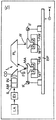
図1は、本発明の特定の実施形態に従ったリソグラフィ投影装置を模式的に示す。本装置は、
EUV放射(例えば、波長が5〜20nmの範囲)の投影ビームPBを供給するための放射システムEx、ILと(この特定の場合、放射システムは放射源LAも備える)、
マスクMA(例えば、レチクル)を保持するためのマスク・ホルダを備え、かつ要素PLに対してマスクを正確に位置決めするための第1の位置決め手段PMに接続された第1の物体テーブル(マスク・テーブル)MTと、
基板W(例えば、レジスト被覆シリコン・ウェーハ)を保持するための基板ホルダを備え、かつ要素PLに対して基板を正確に位置決めするための第2の位置決め手段PWに接続された第2の物体テーブル(基板テーブル)WTと、
マスクMAの放射照射部分の像を、基板Wの目標部分C(例えば、1つまたは複数のダイを含む)に形成するための投影システム(「レンズ」)PLとを備える。
【0019】
ここに示すように、この装置は反射型(すなわち、反射マスクを有する)である。しかし、一般に、装置は例えば透過型(透過マスクを有する)であってもよい。もしくは、装置は、上で言及したようなプログラマブル・ミラー・アレイの型のような、別の種類のパターン形成手段を使用することができる。
【0020】
放射源LA(例えば、レーザ生成プラズマ源または放電プラズマ源)は、放射ビームを生成する。このビームは、直接か、例えばビーム拡大器Exのような条件付け手段を通り抜けた後で、照明システム(照明装置)ILに送られる。照明装置ILは、ビームの強度分布の外側半径範囲および/または内側半径範囲(一般に、σ−outerおよびσ−innerと呼ばれる)を設定するための調整手段AMを含むことができる。さらに、照明装置は、一般に、積分器INおよび集光器COのような様々な他の部品を含む。このようにして、マスクMAに当たるビームPBは、その断面に所望の一様性および強度分布を有する。
【0021】
図1に関して留意すべきことであるが、放射源LAは、リソグラフィ投影装置のハウジング内にあるかもしれないが(放射源LAが例えば水銀ランプである場合、しばしばそうであるように)、放射源は、また、リソグラフィ投影装置から遠く離れており、それが生成する放射ビームが装置の中に導かれるかもしれない(例えば適切な方向付けミラーを使って)。この後者のシナリオは、放射源LAがエキシマ・レーザである場合に、しばしばそうである。本発明および特許請求の範囲は、これらのシナリオの両方を含む。
【0022】
ビームPBは、その後、マスク・テーブルMT上に保持されているマスクMAに遮断される。マスクMAにより選択的に反射されたビームPBは、レンズPLを通り抜ける。このレンズPLは、基板Wの目標部分CにビームPBを収束させる。第2の位置決め手段PW(および干渉測定手段IF)を使って、基板テーブルWTは、例えば、ビームPBの経路内に異なった目標部分Cを位置決めするように、正確に移動させることができる。同様に、第1の位置決め手段PMを使用して、例えば、マスク・ライブラリからマスクMAを機械的に取り出した後で、または走査中に、ビームPBの経路に対してマスクMAを正確に位置決めすることができる。一般に、物体テーブルMT、WTの移動は、長行程モジュール(粗い位置決め)と短行程モジュール(精密位置決め)を使って行われる。これらのモジュールは、図1に明示的に示さない。しかし、ウェーハ・ステッパの場合(走査ステップ式装置に対立するものとして)、マスク・テーブルMTは短行程アクチュエータに接続されるだけかもしれないし、または混在しているかもしれない。
【0023】
図示の装置は、2つの異なるモードで使用することができる。
1.ステップ・モードでは、マスク・テーブルMTは基本的に静止したままであり、全マスク像が一括して(すなわち、単一「フラッシュ」で)目標部分Cに投影される。次に、異なる目標部分CがビームPBで照射されるように、基板テーブルWTがxおよび/またはy方向に移動される。
2.走査モードでは、基本的に同じシナリオが当てはまるが、ただ、特定の目標部分Cが単一「フラッシュ」で露出されないことが異なる。代わりに、マスク・テーブルMTが、特定の方向(いわゆる「走査方向」、例えば、y方向)に速度vで移動可能であり、その結果、投影ビームPBはマスク像全体を走査することができるようになる。これと並行して、基板テーブルWTが、速度V=mvで、同じ方向または反対方向に同時に移動する。ここで、MはレンズPLの拡大率である(通常は、M=1/4または1/5)。このようにして、分解能で妥協する必要なく、比較的大きな目標部分Cを露出させることができる。
【0024】
EUV放射は、使用される光学部品に保護環境を提供するほとんどの気体で大いに吸収されるので、装置は大部分が真空環境中に含まれており、この真空環境は一般にいくつかの副区画に分割されている。
【0025】
図2は、マスク保管ボックス10を示し、このボックス中には、EUV反射マスクが、移送、保管および取り扱いの目的のために格納されている。保管ボックス10は、上部11および底部12を備える。マスクMAは、例えば、ヨーロッパ特許出願EP01301864.3に開示されているような運動学的に決定される保持機構によって、底板12の上の保管ボックス10の内側に保持される。このヨーロッパ特許出願EP01301864.3は、参照してここに組み込む。保管ボックス10の内部には、例えば周囲圧力より高い圧力で保護(不活性)気体の雰囲気を維持することができる。しかし、保管ボックス10の内部に真空を維持することもできる。後者の場合、具体的には、底板12と上部11の間に十分な封止を設けて、保管ボックスの内部とその周囲環境の間の気体の流れおよび、保管ボックスの結果として生じる汚染された内部環境を防止するのが好ましい。
【0026】
保管ボックス10からリソグラフィ投影装置にマスクを移送するために、保管ボックスを、図3に示すいわゆるロード・ロック20の上に置く。ロード・ロック20は、弁30によって図1のリソグラフィ装置の真空環境VCに結合される。この弁30を図4および5にさらに示す。保管ボックスの底板12がロード・ロックの開放可能な上部21と正確に重なるように、保管ボックス10をロード・ロック20の上に位置付けする。このために、案内機構(図示しない)を、ロード・ロックおよび/または保管ボックスに設けて、保管ボックスとロード・ロックの開放可能な上部を適切に位置合わせすることができる。保管ボックス10が適切に位置付けされたときに、保管ボックスをロード・ロックに締め付けるように、締め付け機構(図示しない)を設けるのが好ましい。保管ボックス10とロード・ロック20の間に、封止材22を図式的に示す。封止材22は、底板12および開放可能な上部12に非常に近接して設けるのが好ましい。
【0027】
保管ボックスの底板12および開放可能な上部21は、今や、互いに接触している。図面に垂直な面での底板と開放可能な上部の断面形状は、実質的に同一形状であるように作られる。したがって、両要素の接触面の形状は一致する。封止材23は、底板12と開放可能な上部21の間の周囲に非常に近接して設けるのが好ましい。ポンプP1は、底板12と開放可能な上部21の間の空間を真空にすることができるように設けるのが好ましい。
【0028】
ロード・ロック20の開放可能な上部21は、開放可能な上部21を上下に動かすためのエレベータ25に取り付けられているのが分かる。上部21が上方にいっぱいに動いてロード・ロック20の上の壁にぶつかって、この壁の一部を構成するようになったとき、上部21をロード・ロック20の上の壁に押し付けて封止するために、封止材24が設けられる。ベロー26は、エレベータ25のまわりで、かつ上部21とロード・ロック20の下の壁の間に設ける。エレベータ25は、それを上下に動かす適切な駆動手段(図示しない)に接続される。別のポンプP2が、ロード・ロック20を真空にするために設けられる。
【0029】
マスク保管ボックス10でマスクをロード・ロック20の中に移すために、次のように始めることができる。最初に、マスクをマスク保管ボックス10の内部に保持する。ボックス内部に格納されるマスクを汚染しないように、保管ボックスの全ての内壁が非常にきれいであることに気をつける。粒子も分子汚染も両方とも、マスクを、リソグラフィ投影装置で投影ビームをパターン形成するのに役に立たないものにする可能性がある。上で述べたように、真空または不活性気体を保管ボックス内部に与えることができる。
【0030】
それから、保管ボックス10は、上で説明したようにロード・ロック20の開放可能な上部21の上に位置付けされる。底板12の汚染された外側表面は、開放可能な上部21の汚染された外側表面に重なる。その間の空間は、真空ポンプP1を使用してエレベータ25を通して真空にする。
【0031】
保管ボックス10の内部の真空空間または気体充填空間に依存して、様々な方法で続けることができる。保管ボックスが真空にされている場合には、上部21を開く前に、最初に、ポンプP2を使用してロード・ロック20を真空にするのが好ましいと思われる。保管ボックスが気体で充填されている場合には、同じく最初にロード・ロック20を真空にし、続いて、エレベータ25を下げて、静かに、または非常に突然に上部21を開いて続けることができる。そのとき、保管ボックスからロード・ロック中への気体の流れが起こり、保管ボックスの突然の気体の流れおよび排気は、マスクに存在しているかもしれない粒子を取り去って、マスクをきれいにするのに役立つ。他の方法は、最初にロード・ロックに(不活性)気体を充填し、続いて上部21を下げ、それからポンプP2を使用してロード・ロックを真空にすることかもしれない。
【0032】
また、ロード・ロックの全ての内側表面が非常にきれいであることに気をつける。上記のように進むことによって、ロード・ロックおよび保管ボックスの結合された内部空間に対して生じる汚染された表面積の量は非常に限られたものになる。そのような汚染表面によって、マスクに汚染が導入されるかもしれないが、また、EUV投影リソグラフィのために必要な分圧(例えば、水および炭化水素の)までの排気時間が劇的に増すかもしれない。
【0033】
図4は、マスク保管ボックスから下ろされたマスクを示す。この図は、さらに、ロード・ロックを投影装置の真空システムの別の部分に結合する側部弁30を示す。開いた位置の弁30によって、マスクを持ち上げ、必要に応じて内部ライブラリ、マスク・テーブルまたは他の場所に運ぶためにグリッパー40の利用が可能になる。グリッパーは、先に言及したEP01301864.3に開示されている。
【0034】
投影装置からマスク保管ボックス中にマスクを取り出すために、ロード・ロックおよび保管ボックスの内部空間が真空にされている間に、グリッパー40は、最初に、マスクMAを、エレベータ25で下ろされている底板12の上に載せる。その後で、弁30を閉めることができる。それから、エレベータが上げられて、底板12がボックスを閉めたときに、マスクを保管ボックスの中に置き、さらに保管ボックス内部の真空空間を維持することができる。ボックス内部にきれいな(不活性)気体の雰囲気を保持するために、ロード・ロックおよび保管ボックスの空間をそのような気体でパージし、その後で、エレベータ25を上げて、マスクMAを保管ボックスの中に置き、ボックスの底部分の所定の位置に底板12を入れて保管ボックスを閉じる。
【0035】
図5は、本発明のさらに他の実施形態を示す。この図は図4と全く同じであるが、ただ、ロード・ロック20の上にあるときのマスク保管ボックスを覆ってカバーを設けたことが異なっている。保管ボックスは、ボックスの内部が真空にされ、かつボックスの周囲環境が真空にされないときに生じる圧力に耐えるように特に設計されていないかもしれない。保管ボックスを覆ってカバー50を設け、さらに、保管ボックス内部の空間およびカバー50と保管ボックスの間の空間の両方を真空にすることで、保管ボックスに対して生じる圧力は全くないか無視できる程度になる。ポンプP3は、カバー50と保管ボックスの上部部分11の間の空間を真空にするために示す。
【0036】
本発明は、単に例として、リソグラフィ投影装置に関して説明した。本発明は、マスクを取り扱い、さらに、上記のように、マスクをマスク保管ボックスから装填し、かつマスク保管ボックス中に取り出す必要のあるどのような他の種類の装置にも使用することができ、例えば、マスク描画装置、マスク検査装置、多層堆積装置、マスク清浄装置などに関しても使用できる。マスク保管ボックスは、専用ホルダで2以上のマスクを含むことができる。
【0037】
さらに、本発明は、処理済みまたは未処理の半導体ウェーハのような基板を、基板用の保管ボックスに搬入し、またそこから搬出する際にも使用することができる。
【0038】
マスクが運ばれる保護環境は、真空環境である必要はなく、乾燥空気、窒素、アルゴン、その他種々のような不活性気体で充填された環境であってもよい。
【0039】
本発明の特定の実施形態を上で説明したが、本発明は、説明したようなものとは別の方法で実施できることが理解されよう。この説明は本発明を制限する意図ではない。
【図面の簡単な説明】
【図1】本発明の実施形態に従ったリソグラフィ投影装置を図式的に示す図である。
【図2】マスクが格納される保管ボックスを図式的に示す図である。
【図3】図1のリソグラフィ装置の真空チャンバに取り付けられたロード・ロック・チャンバ上の保管ボックスを図式的に示す図である。
【図4】マスクがロード・ロック・チャンバの中に下ろされている状態の、図3のロード・ロック・チャンバ上の保管ボックスを図式的に示す図である。
【図5】追加の蓋が保管ボックスを覆っている状態の、図4に従った保管ボックスおよびロード・ロック・チャンバを図式的に示す図である。
【符号の説明】
LA 放射源
IL 照明装置
IL 放射システム
PL 投影システム
MA マスク(レチクル)
MT マスク・テーブル
C 目標部分
PB 投影ビーム
W 基板
WT 基板テーブル
10 保管ボックス
11 保管ボックスの上部
12 底板
20 ロード・ロック
21 開放可能な上部
22、23、24 封止材
25 エレベータ
26 ベロー
30 弁
50 カバー
P1、P2、P3 ポンプ[0001]
BACKGROUND OF THE INVENTION
The present invention relates to a method of transporting a substrate or mask suitable for patterning a projection beam of extreme ultraviolet electromagnetic radiation, a storage box, device or apparatus adapted for use in such a method, for example a lithographic projection apparatus. The lithographic projection apparatus
A radiation system for supplying a projection beam of extreme ultraviolet electromagnetic radiation;
A mask table for holding a reflective mask that acts to pattern the projection beam according to a desired pattern when the projection beam reflects off the mask, creating a patterned projection beam;
A substrate table for holding the substrate;
A projection system is provided for projecting the patterned projection beam onto a target portion of the substrate.
[0002]
[Prior art]
Lithographic projection apparatus can be used, for example, in the manufacture of integrated circuits (ICs). In such a case, the pattern forming means can generate circuit patterns corresponding to the individual layers of the IC. An image of this pattern is formed on a target portion (eg composed of one or more chips) on a substrate (silicon wafer) covered with a layer of radiation sensitive material (resist). In general, a single wafer will contain a whole network of adjacent target portions that are successively irradiated via the projection system, one at a time. In current devices where patterning with a mask on a mask table is used, two different types of machines can be distinguished. In one type of lithographic projection apparatus, each target portion is irradiated by exposing all mask patterns to the target portion at once. Such an apparatus is commonly referred to as a wafer stepper. In the other apparatus, commonly referred to as a scanning stepped apparatus, the mask pattern impinged by the projection beam is scanned progressively in a given reference direction ("scan" direction) and simultaneously, synchronously and parallel to this direction. Alternatively, each target portion is irradiated by scanning the substrate table in antiparallel. In general, since the projection system has a magnification factor M (generally M <1), the speed V at which the substrate table is scanned is a factor M times the speed at which the mask table is scanned. More information can be gathered on a lithographic apparatus as here described, for example from US Pat. No. 6,046,792. This patent is incorporated herein by reference.
[0003]
In a manufacturing process using a lithographic projection apparatus, an image of a pattern (eg in a mask) is created on a substrate that is at least partially covered by a layer of radiation sensitive material (resist). Prior to this imaging step, the substrate can go through various procedures such as primering, resist coating, and soft baking. After exposure, the substrate can be subjected to other procedures such as post-exposure bake (PEB), development, hard bake, and measurement / inspection of the characteristics of the formed image. This sequence of procedures is used as a basis for patterning individual layers of a device, eg, an IC. Such patterned layers then go through various processes, all intended to finish individual layers, such as etching, ion implantation (doping), metallization, oxidation, chemical mechanical polishing, etc. Can do. If several layers are required, this entire procedure or a variation thereof must be repeated for each new layer. Eventually, an array of devices will be present on the substrate (wafer). These devices can then be separated from each other in a manner such as dicing or sawing, and then the individual devices can be attached to a carrier connected to pins or the like. More information on such processes can be found in, for example, “Microchip Fabrication: A Practical Guide to Semiconductor Processing”, Third Edition, by Peter Van Gant Hant Zan, Publishing Co. 1997, ISBN 0-07-0667250-4. This book is incorporated herein by reference.
[0004]
For simplicity, the projection system may be referred to below as a “lens”. However, this term should be broadly interpreted as encompassing various types of projection systems such as refractive optical systems, reflective optical systems, and catadioptric systems. The radiation system can also include components that operate according to any of these design schemes to direct, shape, or control the projected beam of radiation. Furthermore, such components may also be referred to collectively as “lenses” below or collectively. Further, the lithographic apparatus may be of a type having two or more substrate tables (and / or two or more mask tables). In such “multi-stage” apparatus, the additional tables may be used in parallel, or one or more while using one or more other tables for exposure. Preparatory steps may be performed at the table. Twin stage lithographic apparatus are described, for example, in US Pat. No. 5,969,441 and International Publication No. WO 98/40791. Both of which are incorporated herein by reference.
[0005]
The concept of a mask is well known in lithography and includes mask types such as binary, alternating phase shift, and attenuated phase shift as well as various hybrid mask types. Placing such a mask in the radiation beam results in selective transmission (in the case of a transmission mask) or selective reflection (in the case of a reflection mask) of radiation striking the mask according to the pattern on the mask. The mask table ensures that the mask can be held in a desired position in the incident radiation beam and, if so desired, the mask can be moved relative to the beam. Become.
[0006]
Traditionally, the mask table has been positioned so that the radiation travels from the illumination system to the substrate through the mask and projection system. Such masks are known as transmission masks because they selectively pass radiation from the illumination system to form a pattern on the substrate. Such a mask must be supported so that light can pass through the mask. In the past, this has been accomplished using a vacuum on the table at the peripheral area of the mask, such as pressing the mask against the mask table with atmospheric air pressure.
[0007]
In a lithographic apparatus, the size of a feature that can form an image on a wafer is limited by the wavelength of the projection radiation. In order to produce integrated circuits with higher density devices and thus higher operating speeds, it is desirable to be able to image smaller features. Most current lithographic projection apparatus use 365 nm, 248 nm and 193 nm ultraviolet light generated by mercury lamps or excimer lasers, but it has been proposed to use shorter wavelength radiation of approximately 13 nm. Yes. Such radiation is referred to as extreme ultraviolet (EUV) radiation, and possible light sources include laser-produced plasma sources, discharge light sources, or synchrotron radiation sources, examples of which are described in, for example, European Patent Application EP 1109427A and It is disclosed in EP1170982A. These applications are incorporated herein by reference.
[0008]
To date, no material is known that is sufficiently transparent to EUV radiation, so that lithographic projection apparatus using EUV radiation can be used for multilayer coatings of alternating layers of different materials, for example molybdenum and silicon or for example European patent applications It is conceivable to use a reflective mask with alternating layers of as many as 50 periods of other materials as disclosed in EP 1065532A. This European patent application EP 1065532A is incorporated herein by reference. Due to the size of the features imaged by EUV lithography, the imaging process becomes very sensitive to contamination present on the mask. Any contamination particles with dimensions on the order of 50 nm are expected to cause defects present in devices fabricated on the substrate. Conventionally, the patterned side of a reticle is covered with a so-called pellicle. So any contamination is deposited on the pellicle surface at a distance from the mask pattern so that no (clearly) image is formed on the substrate and such a mask with a pellicle is less sensitive to contamination. ing. The pellicle cannot be used for EUV radiation because it is not sufficiently transparent to EUV radiation. Therefore, particle contamination of the reflective surface of the mask containing the pattern should be avoided since it results in the manufacture of defective devices.
[0009]
Furthermore, it is conceivable that the back side of the mask is fixed to the mask table by an electrostatic force acting on the mask support surface so that the reflection mask can satisfy very severe conditions of EUV mask positioning. Contaminant particles present between the back side of the mask and the mask support surface of the mask table cause irregularities on the reflective mask surface. Since the projection system is not telecentric on the object side because a reflective mask is used (more information about this problem can be obtained from European patent application EP 1139176A, which is incorporated herein by reference. ), Irregularities in the surface shape of the reflective mask surface lead to local shifts in the pattern in which an image is formed on the substrate. As a result, the imaged layer may again not be aligned with the previous layer that was processed into the substrate, thus again leading to the production of defective devices. Therefore, particle contamination on the backside surface of the mask must not occur.
[0010]
Molecular type contamination such as hydrocarbons and water should also be avoided. Such contamination adversely affects the optical components of the lithographic apparatus, such as a mask. Care should be taken in all handling procedures of the mask and substrate to keep the surface of the mask and substrate free from such molecular contamination. Masks and substrates can be stored and transferred between various types of equipment using a storage box that is maintained in a protective environment, such as an environment that is evacuated or filled with an inert gas. it can. The inner wall of such a storage box should also remain uncontaminated. However, while removing the mask or substrate from such a storage box and processing or transferring such a substrate or mask to the device or apparatus used, both particle and molecular contamination are It may occur on the substrate or the inner wall of the protective environment. The mask or substrate can be transferred through an intermediate chamber, such as a load lock chamber, to the final environment for processing or use, but before such contamination is removed from the intermediate chamber for a very long time, such as It may take a very long exhaust time when evacuating the protective environment.
[0011]
[Problems to be solved by the invention]
The object of the present invention is to provide a transfer method in which the introduction of contamination into the protected environment is greatly reduced or even completely eliminated.
[0012]
[Means for Solving the Problems]
This and other objects are directed to a method for transferring one or more substrates or masks in a storage box to a device or apparatus for handling, processing or using said substrates or masks, or vice versa. This is achieved according to the present invention. The storage box comprises a lid having an openable lid portion, the method comprising:
The storage box is placed on an openable wall portion of a sealed protective environment wall of the device or apparatus, and the openable lid portion of the storage box is the open of the protective environment. Attaching to a possible wall portion, wherein the protective environment is configured to be filled with an inert gas or to be evacuated;
Opening said releasable lid portion of said storage box and said releasable wall portion of said protective environment, whereby said lid of said storage box is said of said protective environment Forming a wall portion of the storage box and the interior of the storage box being part of the protective environment;
Transferring at least one of the substrate or mask from an interior space of the storage box to an interior space of the wall of the protective environment, or vice versa.
[0013]
In accordance with yet another aspect of the present invention, a storage box and device or apparatus for use in the above method are provided.
[0014]
According to yet another aspect of the invention,
Providing a substrate that is at least partially covered by a layer of radiation-sensitive material;
Providing a projection beam of extreme ultraviolet radiation using a radiation system;
Using a reflective mask to provide a pattern in the cross section of the projection beam to provide a beam of patterned radiation;
A device manufacturing method is provided comprising projecting a beam of patterned radiation onto a target portion of a layer of radiation sensitive material and transferring one or more masks or substrates according to the method described above.
[0015]
While this specification may specifically refer to the use of a device according to the present invention in the manufacture of an IC, it should be clearly understood that such a device has many other possible uses. is there. For example, it can be used in integrated optical systems, magnetic domain memory guidance and detection, liquid crystal display panels, thin film magnetic heads, and others. As those skilled in the art will appreciate, in such other application environments, the use of the terms “reticle”, “wafer” or “chip” in this specification is the more general term “mask”, It should be considered as being replaced by “substrate” and “target part”, respectively.
[0016]
In this document, the terms “radiation” and “beam” are used to encompass extreme ultraviolet (EUV) radiation having a wavelength in the range of 5-20 nm, for example.
[0017]
Embodiments of the invention will now be described, by way of example only, with reference to the accompanying schematic drawings. Corresponding reference characters indicate corresponding parts in the drawings.
[0018]
DETAILED DESCRIPTION OF THE INVENTION
FIG. 1 schematically depicts a lithographic projection apparatus according to a particular embodiment of the invention. This device
A radiation system Ex, IL for supplying a projection beam PB of EUV radiation (eg in the range of 5-20 nm in wavelength) (in this particular case, the radiation system also comprises a radiation source LA);
A first object table (mask mask) comprising a mask holder for holding a mask MA (eg a reticle) and connected to first positioning means PM for accurately positioning the mask with respect to the element PL Table) MT,
A second object table comprising a substrate holder for holding a substrate W (eg resist-coated silicon wafer) and connected to second positioning means PW for accurately positioning the substrate relative to the element PL (Substrate table) WT;
And a projection system (“lens”) PL for forming an image of the irradiated portion of the mask MA on a target portion C (eg, including one or more dies) of the substrate W.
[0019]
As shown here, the apparatus is of a reflective type (ie having a reflective mask). However, in general, the apparatus may be of a transmissive type (having a transmissive mask), for example. Alternatively, the apparatus can use another type of patterning means, such as a programmable mirror array type as mentioned above.
[0020]
The radiation source LA (eg, a laser-produced plasma source or a discharge plasma source) generates a radiation beam. This beam is sent to the illumination system (illuminator) IL either directly or after passing through conditioning means such as a beam expander Ex. The illuminator IL may include adjusting means AM for setting an outer radius range and / or an inner radius range (commonly referred to as σ-outer and σ-inner) of the intensity distribution of the beam. In addition, the illumination device typically includes various other components such as an integrator IN and a condenser CO. In this way, the beam PB hitting the mask MA has a desired uniformity and intensity distribution in its cross section.
[0021]
It should be noted with respect to FIG. 1 that the source LA may be in the housing of the lithographic projection apparatus (as is often the case when the source LA is a mercury lamp, for example) May also be far from the lithographic projection apparatus and the radiation beam it generates may be directed into the apparatus (eg, using a suitable directing mirror). This latter scenario is often the case when the source LA is an excimer laser. The present invention and claims include both of these scenarios.
[0022]
The beam PB is then interrupted by the mask MA, which is held on the mask table MT. The beam PB selectively reflected by the mask MA passes through the lens PL. The lens PL converges the beam PB on the target portion C of the substrate W. Using the second positioning means PW (and the interference measuring means IF), the substrate table WT can be accurately moved, for example, to position different target portions C in the path of the beam PB. Similarly, the first positioning means PM is used to accurately position the mask MA with respect to the path of the beam PB, for example after mechanical removal of the mask MA from the mask library or during a scan. be able to. In general, the movement of the object tables MT, WT is performed using a long stroke module (coarse positioning) and a short stroke module (fine positioning). These modules are not explicitly shown in FIG. However, in the case of a wafer stepper (as opposed to a scanning stepper), the mask table MT may only be connected to a short stroke actuator or may be mixed.
[0023]
The depicted apparatus can be used in two different modes.
1. In step mode, the mask table MT remains essentially stationary and the entire mask image is projected onto the target portion C in bulk (ie, with a single “flash”). The substrate table WT is then moved in the x and / or y direction so that a different target portion C is irradiated with the beam PB.
2. In scan mode, basically the same scenario applies, except that a specific target portion C is not exposed in a single “flash”. Instead, the mask table MT can be moved at a velocity v in a specific direction (so-called “scanning direction”, eg the y direction) so that the projection beam PB can scan the entire mask image. become. In parallel with this, the substrate table WT moves simultaneously in the same direction or in the opposite direction at a velocity V = mv. Here, M is an enlargement ratio of the lens PL (usually M = 1/4 or 1/5). In this way, a relatively large target portion C can be exposed without having to compromise on resolution.
[0024]
Since EUV radiation is greatly absorbed by most gases that provide a protective environment for the optical components used, the device is mostly contained in a vacuum environment, which is generally in several subcompartments. It is divided.
[0025]
FIG. 2 shows a
[0026]
In order to transfer the mask from the
[0027]
The storage
[0028]
It can be seen that the openable
[0029]
To move the mask into the
[0030]
The
[0031]
Depending on the vacuum space or gas-filled space inside the
[0032]
Also note that all inner surfaces of the load lock are very clean. By proceeding as described above, the amount of contaminated surface area generated for the combined interior space of the load lock and storage box is very limited. Such a contaminated surface may introduce contamination into the mask, but may also dramatically increase the exhaust time to the partial pressure (eg, water and hydrocarbons) required for EUV projection lithography. unknown.
[0033]
FIG. 4 shows the mask lowered from the mask storage box. This figure further shows a
[0034]
In order to remove the mask from the projection device into the mask storage box, the
[0035]
FIG. 5 shows yet another embodiment of the present invention. This figure is exactly the same as FIG. 4 except that a cover is provided over the mask storage box when over the
[0036]
The invention has been described by way of example only with reference to a lithographic projection apparatus. The present invention can be used in any other type of apparatus that handles a mask and further requires that the mask be loaded and removed from the mask storage box as described above, For example, it can be used for a mask drawing apparatus, a mask inspection apparatus, a multilayer deposition apparatus, a mask cleaning apparatus, and the like. The mask storage box can include two or more masks with a dedicated holder.
[0037]
Furthermore, the present invention can be used when a substrate such as a processed or unprocessed semiconductor wafer is carried into and out of a storage box for the substrate.
[0038]
The protective environment in which the mask is carried need not be a vacuum environment, but may be an environment filled with an inert gas such as dry air, nitrogen, argon, or the like.
[0039]
While specific embodiments of the invention have been described above, it will be appreciated that the invention may be practiced otherwise than as described. This description is not intended to limit the invention.
[Brief description of the drawings]
FIG. 1 schematically depicts a lithographic projection apparatus according to an embodiment of the invention.
FIG. 2 is a diagram schematically showing a storage box in which a mask is stored.
FIG. 3 schematically depicts a storage box on a load lock chamber attached to the vacuum chamber of the lithographic apparatus of FIG.
4 schematically illustrates a storage box on the load lock chamber of FIG. 3 with the mask being lowered into the load lock chamber. FIG.
5 schematically shows the storage box and load lock chamber according to FIG. 4 with an additional lid covering the storage box.
[Explanation of symbols]
LA radiation source
IL lighting device
IL radiation system
PL projection system
MA mask (reticle)
MT mask table
C Target part
PB projection beam
W substrate
WT board table
10 Storage box
11 Top of storage box
12 Bottom plate
20 Load lock
21 Openable top
22, 23, 24 Sealing material
25 Elevator
26 Bellows
30 valves
50 cover
P1, P2, P3 pump
Claims (7)
前記保管ボックスを、前記ロード・ロックの前記開放可能な壁部分の上に、前記保管ボックスの前記開放可能な蓋部分が前記保護環境の前記開放可能な壁部分と重なるように取り付けるステップであって、前記保管ボックスの前記開放可能な蓋部分と前記保護環境の前記開放可能な壁部分との間には、周囲に近接して封止材が配置され、該蓋部分と該壁部分との間の空間は、前記第1の真空ポンプを使用して前記エレベータを通して真空にされるとともに、前記ロード・ロックが前記第2の真空ポンプを使用して真空にされるように構成されているものであるステップと、
前記保管ボックスの前記開放可能な蓋部分および前記ロード・ロックの前記開放可能な壁部分を開くステップであって、前記エレベータを移動させて前記蓋部分及び前記壁部分を下げることにより、前記蓋部分が開かれた前記保管ボックスの前記蓋が、前記保護環境の開かれた前記壁部分に代わって前記保護環境を密閉し、前記保管ボックスの内部を前記保護環境に連通させるステップと、
前記保管ボックスの内部空間から前記保護環境の前記壁の内部空間に、またはその逆に前記基板またはマスクの少なくとも1つを移すステップとを特徴とする方法。One or more substrate or mask using a storage box, or transferred from the storage box to the load lock handling the substrate or mask, or a method of transferring the storage box from the load lock, the A storage box is removable from the load lock , the storage box further comprising a lid having an openable lid portion, wherein the load lock includes an openable wall portion of the wall of the sealed storage environment; An elevator for opening and closing the wall portion; first and second vacuum pumps; and a side valve for coupling the load lock to another vacuum system;
Mounting the storage box on the openable wall portion of the load lock so that the openable lid portion of the storage box overlaps the openable wall portion of the protective environment; A sealant is disposed between the openable lid portion of the storage box and the openable wall portion of the protective environment in proximity to the periphery, between the lid portion and the wall portion; The space is configured to be evacuated through the elevator using the first vacuum pump and the load lock is evacuated using the second vacuum pump. A step and
Opening the openable lid portion of the storage box and the openable wall portion of the load lock by moving the elevator to lower the lid portion and the wall portion; The lid of the storage box opened by sealing the protective environment on behalf of the open wall portion of the protective environment and communicating the interior of the storage box to the protective environment;
Transferring at least one of the substrate or mask from an interior space of the storage box to an interior space of the wall of the protective environment, or vice versa.
少なくとも部分的に放射敏感材料の層で覆われた基板を供給するステップと、
放射システムを使用して極端紫外放射の投影ビームを供給するステップと、
パターン形成された放射のビームを供給するために、前記投影ビームの断面にパターンを与えるように反射マスクを使用するステップと、
前記パターン形成された放射のビームを放射敏感材料の前記層の目標部分に投影するステップと、
請求項1から請求項6までのいずれか一項に記載の方法に従って、1つまたは複数のマスクまたは基板を移すステップとを含む方法。A device manufacturing method comprising:
Providing a substrate at least partially covered with a layer of radiation sensitive material;
Providing a projection beam of extreme ultraviolet radiation using a radiation system;
Using a reflective mask to provide a pattern in a cross-section of the projection beam to provide a beam of patterned radiation;
Projecting the patterned beam of radiation onto a target portion of the layer of radiation sensitive material;
7. Transferring one or more masks or substrates according to the method of any one of claims 1-6.
Applications Claiming Priority (1)
| Application Number | Priority Date | Filing Date | Title |
|---|---|---|---|
| EP02075883 | 2002-03-01 |
Publications (2)
| Publication Number | Publication Date |
|---|---|
| JP2004006784A JP2004006784A (en) | 2004-01-08 |
| JP4030452B2 true JP4030452B2 (en) | 2008-01-09 |
Family
ID=29558351
Family Applications (1)
| Application Number | Title | Priority Date | Filing Date |
|---|---|---|---|
| JP2003100900A Expired - Fee Related JP4030452B2 (en) | 2002-03-01 | 2003-02-27 | Mask or substrate transfer method, storage box, device or apparatus adapted for use in such a method, and device manufacturing method including such a method |
Country Status (6)
| Country | Link |
|---|---|
| US (1) | US6753945B2 (en) |
| JP (1) | JP4030452B2 (en) |
| KR (1) | KR100588121B1 (en) |
| CN (1) | CN1474233A (en) |
| SG (1) | SG106129A1 (en) |
| TW (1) | TWI247337B (en) |
Families Citing this family (27)
| Publication number | Priority date | Publication date | Assignee | Title |
|---|---|---|---|---|
| DE10261775A1 (en) | 2002-12-20 | 2004-07-01 | Carl Zeiss Smt Ag | Device for the optical measurement of an imaging system |
| US20050169730A1 (en) * | 2003-04-30 | 2005-08-04 | Ravinder Aggarwal | Semiconductor processing tool front end interface with sealing capability |
| US7026581B2 (en) * | 2003-08-22 | 2006-04-11 | Axcelis Technologies, Inc. | Apparatus for positioning an elevator tube |
| TW201809911A (en) | 2003-09-29 | 2018-03-16 | 尼康股份有限公司 | Exposure apparatus, exposure method, and method for producing device |
| WO2005047981A2 (en) * | 2003-11-10 | 2005-05-26 | Nikon Corporation | Thermophoretic techniques for protecting reticles from contaminants |
| WO2005119368A2 (en) | 2004-06-04 | 2005-12-15 | Carl Zeiss Smt Ag | System for measuring the image quality of an optical imaging system |
| US20060033905A1 (en) * | 2004-08-16 | 2006-02-16 | Mahmood Toofan | Pellicle-reticle methods with reduced haze or wrinkle formation |
| EP1786342A1 (en) * | 2004-09-07 | 2007-05-23 | Smith and Nephew, Inc. | Minimal thickness bone plate locking mechanism |
| US7477358B2 (en) * | 2004-09-28 | 2009-01-13 | Nikon Corporation | EUV reticle handling system and method |
| JP2006128188A (en) * | 2004-10-26 | 2006-05-18 | Nikon Corp | Substrate carrying apparatus, substrate carrying method and exposure apparatus |
| JP4710308B2 (en) | 2004-10-29 | 2011-06-29 | 株式会社ニコン | Reticle conveying apparatus, exposure apparatus, and reticle conveying method |
| US7428958B2 (en) * | 2004-11-15 | 2008-09-30 | Nikon Corporation | Substrate conveyor apparatus, substrate conveyance method and exposure apparatus |
| TWI447840B (en) * | 2004-11-15 | 2014-08-01 | 尼康股份有限公司 | Substrate transport device, substrate transport method and exposure device |
| US20060201958A1 (en) * | 2005-02-27 | 2006-09-14 | Tieben Anthony M | Mask container |
| JP4667140B2 (en) * | 2005-06-30 | 2011-04-06 | キヤノン株式会社 | Exposure apparatus and device manufacturing method |
| US7665981B2 (en) | 2005-08-25 | 2010-02-23 | Molecular Imprints, Inc. | System to transfer a template transfer body between a motion stage and a docking plate |
| US7808616B2 (en) * | 2005-12-28 | 2010-10-05 | Nikon Corporation | Reticle transport apparatus, exposure apparatus, reticle transport method, and reticle processing method |
| US7773198B2 (en) * | 2006-03-28 | 2010-08-10 | Nikon Corporation | Filtered device container assembly with shield for a reticle |
| US7740437B2 (en) | 2006-09-22 | 2010-06-22 | Asm International N.V. | Processing system with increased cassette storage capacity |
| US20080128303A1 (en) * | 2006-12-05 | 2008-06-05 | Nikon Corporation | Device container assembly with adjustable retainers for a reticle |
| US10586722B2 (en) * | 2007-05-30 | 2020-03-10 | Brooks Automation, Inc. | Vacuum substrate storage |
| JP5516968B2 (en) * | 2010-06-08 | 2014-06-11 | 独立行政法人産業技術総合研究所 | Linked transport system |
| KR101293025B1 (en) | 2011-12-22 | 2013-08-05 | 에스엔유 프리시젼 주식회사 | Mask Stock and Panel Passage Chamber, Method for Operating the same |
| US8968971B2 (en) | 2013-03-08 | 2015-03-03 | Micro Lithography, Inc. | Pellicles with reduced particulates |
| US10459352B2 (en) | 2015-08-31 | 2019-10-29 | Taiwan Semiconductor Manufacturing Company, Ltd. | Mask cleaning |
| US11226568B2 (en) * | 2017-11-09 | 2022-01-18 | Asml Netherlands B.V. | Lithographic apparatus and method |
| KR102388390B1 (en) * | 2020-01-06 | 2022-04-21 | 세메스 주식회사 | Load port unit, storage apparatus comprising the same and exhaust method |
Family Cites Families (7)
| Publication number | Priority date | Publication date | Assignee | Title |
|---|---|---|---|---|
| EP0358443B1 (en) | 1988-09-06 | 1997-11-26 | Canon Kabushiki Kaisha | Mask cassette loading device |
| US5169272A (en) | 1990-11-01 | 1992-12-08 | Asyst Technologies, Inc. | Method and apparatus for transferring articles between two controlled environments |
| US5559584A (en) | 1993-03-08 | 1996-09-24 | Nikon Corporation | Exposure apparatus |
| US6427096B1 (en) * | 1999-02-12 | 2002-07-30 | Honeywell International Inc. | Processing tool interface apparatus for use in manufacturing environment |
| JP3513437B2 (en) | 1999-09-01 | 2004-03-31 | キヤノン株式会社 | Substrate management method and semiconductor exposure apparatus |
| AU4462001A (en) | 2000-03-29 | 2001-10-08 | Nikon Corporation | Aligner, apparatus and method for transferring wafer, microdevice and method formanufacturing the same |
| KR100592576B1 (en) * | 2000-06-02 | 2006-06-26 | 에이에스엠엘 네델란즈 비.브이. | Lithographic projection apparatus, supporting assembly and device manufacturing method |
-
2003
- 2003-02-27 US US10/374,511 patent/US6753945B2/en not_active Expired - Lifetime
- 2003-02-27 SG SG200300824A patent/SG106129A1/en unknown
- 2003-02-27 TW TW092104242A patent/TWI247337B/en not_active IP Right Cessation
- 2003-02-27 CN CNA031107818A patent/CN1474233A/en active Pending
- 2003-02-27 JP JP2003100900A patent/JP4030452B2/en not_active Expired - Fee Related
- 2003-02-27 KR KR1020030012302A patent/KR100588121B1/en active IP Right Grant
Also Published As
| Publication number | Publication date |
|---|---|
| KR100588121B1 (en) | 2006-06-09 |
| US20030224295A1 (en) | 2003-12-04 |
| TW200307980A (en) | 2003-12-16 |
| CN1474233A (en) | 2004-02-11 |
| KR20030071632A (en) | 2003-09-06 |
| TWI247337B (en) | 2006-01-11 |
| SG106129A1 (en) | 2004-09-30 |
| JP2004006784A (en) | 2004-01-08 |
| US6753945B2 (en) | 2004-06-22 |
Similar Documents
| Publication | Publication Date | Title |
|---|---|---|
| JP4030452B2 (en) | Mask or substrate transfer method, storage box, device or apparatus adapted for use in such a method, and device manufacturing method including such a method | |
| US8235212B2 (en) | Mask transport system configured to transport a mask into and out of a lithographic apparatus | |
| US8347915B2 (en) | Load-lock technique | |
| JP4021419B2 (en) | Temperature controlled load lock, lithographic apparatus with load lock, and method of manufacturing a substrate using the load lock | |
| JP2004247733A (en) | Lithography apparatus including gas washing system | |
| US7656507B2 (en) | Processing unit, exposure apparatus having the processing unit, and protection unit | |
| JP4154380B2 (en) | Lithographic apparatus and device manufacturing method | |
| JP3836751B2 (en) | Lithographic projection apparatus, element manufacturing method, and element manufactured thereby | |
| US7230673B2 (en) | Lithographic apparatus, reticle exchange unit and device manufacturing method | |
| EP1434094A1 (en) | Container for a mask | |
| WO2002069379A1 (en) | X-ray reflective mask, method of protecting the reflective mask, x-ray exposure device, and method of manufacturing semiconductor device | |
| TWI232356B (en) | Lithographic projection apparatus, device manufacturing method and device manufactured thereby | |
| TWI289733B (en) | Lithographic apparatus and device manufacturing method | |
| EP1341045A1 (en) | Method of transferring a mask or substrate | |
| US7088421B2 (en) | Lithographic apparatus, device manufacturing method, and device manufactured thereby | |
| JP2007165778A (en) | Exposing apparatus | |
| JP3713479B2 (en) | Flat projection apparatus and element manufacturing method | |
| EP1396759A2 (en) | Lithographic apparatus, device manufacturing method, and device manufactured thereby | |
| JP2007142019A (en) | Exposure device |
Legal Events
| Date | Code | Title | Description |
|---|---|---|---|
| A131 | Notification of reasons for refusal |
Free format text: JAPANESE INTERMEDIATE CODE: A131 Effective date: 20050419 |
|
| A601 | Written request for extension of time |
Free format text: JAPANESE INTERMEDIATE CODE: A601 Effective date: 20050719 |
|
| A602 | Written permission of extension of time |
Free format text: JAPANESE INTERMEDIATE CODE: A602 Effective date: 20050722 |
|
| A521 | Written amendment |
Free format text: JAPANESE INTERMEDIATE CODE: A523 Effective date: 20050921 |
|
| A02 | Decision of refusal |
Free format text: JAPANESE INTERMEDIATE CODE: A02 Effective date: 20060307 |
|
| A521 | Written amendment |
Free format text: JAPANESE INTERMEDIATE CODE: A523 Effective date: 20060605 |
|
| A521 | Written amendment |
Free format text: JAPANESE INTERMEDIATE CODE: A523 Effective date: 20060705 |
|
| RD03 | Notification of appointment of power of attorney |
Free format text: JAPANESE INTERMEDIATE CODE: A7423 Effective date: 20060904 |
|
| A911 | Transfer to examiner for re-examination before appeal (zenchi) |
Free format text: JAPANESE INTERMEDIATE CODE: A911 Effective date: 20060929 |
|
| A912 | Re-examination (zenchi) completed and case transferred to appeal board |
Free format text: JAPANESE INTERMEDIATE CODE: A912 Effective date: 20061208 |
|
| A61 | First payment of annual fees (during grant procedure) |
Free format text: JAPANESE INTERMEDIATE CODE: A61 Effective date: 20071016 |
|
| R150 | Certificate of patent or registration of utility model |
Ref document number: 4030452 Country of ref document: JP Free format text: JAPANESE INTERMEDIATE CODE: R150 Free format text: JAPANESE INTERMEDIATE CODE: R150 |
|
| FPAY | Renewal fee payment (event date is renewal date of database) |
Free format text: PAYMENT UNTIL: 20101026 Year of fee payment: 3 |
|
| FPAY | Renewal fee payment (event date is renewal date of database) |
Free format text: PAYMENT UNTIL: 20101026 Year of fee payment: 3 |
|
| FPAY | Renewal fee payment (event date is renewal date of database) |
Free format text: PAYMENT UNTIL: 20111026 Year of fee payment: 4 |
|
| R250 | Receipt of annual fees |
Free format text: JAPANESE INTERMEDIATE CODE: R250 |
|
| FPAY | Renewal fee payment (event date is renewal date of database) |
Free format text: PAYMENT UNTIL: 20111026 Year of fee payment: 4 |
|
| FPAY | Renewal fee payment (event date is renewal date of database) |
Free format text: PAYMENT UNTIL: 20121026 Year of fee payment: 5 |
|
| R250 | Receipt of annual fees |
Free format text: JAPANESE INTERMEDIATE CODE: R250 |
|
| FPAY | Renewal fee payment (event date is renewal date of database) |
Free format text: PAYMENT UNTIL: 20121026 Year of fee payment: 5 |
|
| FPAY | Renewal fee payment (event date is renewal date of database) |
Free format text: PAYMENT UNTIL: 20131026 Year of fee payment: 6 |
|
| R250 | Receipt of annual fees |
Free format text: JAPANESE INTERMEDIATE CODE: R250 |
|
| R250 | Receipt of annual fees |
Free format text: JAPANESE INTERMEDIATE CODE: R250 |
|
| R250 | Receipt of annual fees |
Free format text: JAPANESE INTERMEDIATE CODE: R250 |
|
| R250 | Receipt of annual fees |
Free format text: JAPANESE INTERMEDIATE CODE: R250 |
|
| R250 | Receipt of annual fees |
Free format text: JAPANESE INTERMEDIATE CODE: R250 |
|
| R250 | Receipt of annual fees |
Free format text: JAPANESE INTERMEDIATE CODE: R250 |
|
| R250 | Receipt of annual fees |
Free format text: JAPANESE INTERMEDIATE CODE: R250 |
|
| R250 | Receipt of annual fees |
Free format text: JAPANESE INTERMEDIATE CODE: R250 |
|
| LAPS | Cancellation because of no payment of annual fees |