EP3423947B1 - Power saving techniques for memory systems - Google Patents
Power saving techniques for memory systems Download PDFInfo
- Publication number
- EP3423947B1 EP3423947B1 EP17711926.0A EP17711926A EP3423947B1 EP 3423947 B1 EP3423947 B1 EP 3423947B1 EP 17711926 A EP17711926 A EP 17711926A EP 3423947 B1 EP3423947 B1 EP 3423947B1
- Authority
- EP
- European Patent Office
- Prior art keywords
- data
- memory
- command
- host processor
- lanes
- Prior art date
- Legal status (The legal status is an assumption and is not a legal conclusion. Google has not performed a legal analysis and makes no representation as to the accuracy of the status listed.)
- Active
Links
Images


Classifications
-
- G—PHYSICS
- G06—COMPUTING OR CALCULATING; COUNTING
- G06F—ELECTRIC DIGITAL DATA PROCESSING
- G06F1/00—Details not covered by groups G06F3/00 - G06F13/00 and G06F21/00
- G06F1/26—Power supply means, e.g. regulation thereof
- G06F1/32—Means for saving power
- G06F1/3203—Power management, i.e. event-based initiation of a power-saving mode
- G06F1/3234—Power saving characterised by the action undertaken
- G06F1/325—Power saving in peripheral device
- G06F1/3275—Power saving in memory, e.g. RAM, cache
-
- G—PHYSICS
- G06—COMPUTING OR CALCULATING; COUNTING
- G06F—ELECTRIC DIGITAL DATA PROCESSING
- G06F1/00—Details not covered by groups G06F3/00 - G06F13/00 and G06F21/00
- G06F1/26—Power supply means, e.g. regulation thereof
- G06F1/32—Means for saving power
- G06F1/3203—Power management, i.e. event-based initiation of a power-saving mode
- G06F1/3206—Monitoring of events, devices or parameters that trigger a change in power modality
- G06F1/3215—Monitoring of peripheral devices
- G06F1/3225—Monitoring of peripheral devices of memory devices
-
- G—PHYSICS
- G06—COMPUTING OR CALCULATING; COUNTING
- G06F—ELECTRIC DIGITAL DATA PROCESSING
- G06F1/00—Details not covered by groups G06F3/00 - G06F13/00 and G06F21/00
- G06F1/26—Power supply means, e.g. regulation thereof
- G06F1/32—Means for saving power
- G06F1/3203—Power management, i.e. event-based initiation of a power-saving mode
- G06F1/3234—Power saving characterised by the action undertaken
- G06F1/325—Power saving in peripheral device
- G06F1/3278—Power saving in modem or I/O interface
-
- G—PHYSICS
- G06—COMPUTING OR CALCULATING; COUNTING
- G06F—ELECTRIC DIGITAL DATA PROCESSING
- G06F12/00—Accessing, addressing or allocating within memory systems or architectures
- G06F12/02—Addressing or allocation; Relocation
- G06F12/06—Addressing a physical block of locations, e.g. base addressing, module addressing, memory dedication
-
- G—PHYSICS
- G06—COMPUTING OR CALCULATING; COUNTING
- G06F—ELECTRIC DIGITAL DATA PROCESSING
- G06F13/00—Interconnection of, or transfer of information or other signals between, memories, input/output devices or central processing units
- G06F13/14—Handling requests for interconnection or transfer
- G06F13/16—Handling requests for interconnection or transfer for access to memory bus
- G06F13/1668—Details of memory controller
- G06F13/1673—Details of memory controller using buffers
-
- G—PHYSICS
- G06—COMPUTING OR CALCULATING; COUNTING
- G06F—ELECTRIC DIGITAL DATA PROCESSING
- G06F13/00—Interconnection of, or transfer of information or other signals between, memories, input/output devices or central processing units
- G06F13/38—Information transfer, e.g. on bus
- G06F13/42—Bus transfer protocol, e.g. handshake; Synchronisation
- G06F13/4204—Bus transfer protocol, e.g. handshake; Synchronisation on a parallel bus
- G06F13/4234—Bus transfer protocol, e.g. handshake; Synchronisation on a parallel bus being a memory bus
-
- G—PHYSICS
- G06—COMPUTING OR CALCULATING; COUNTING
- G06F—ELECTRIC DIGITAL DATA PROCESSING
- G06F3/00—Input arrangements for transferring data to be processed into a form capable of being handled by the computer; Output arrangements for transferring data from processing unit to output unit, e.g. interface arrangements
- G06F3/06—Digital input from, or digital output to, record carriers, e.g. RAID, emulated record carriers or networked record carriers
- G06F3/0601—Interfaces specially adapted for storage systems
- G06F3/0602—Interfaces specially adapted for storage systems specifically adapted to achieve a particular effect
- G06F3/0608—Saving storage space on storage systems
-
- G—PHYSICS
- G06—COMPUTING OR CALCULATING; COUNTING
- G06F—ELECTRIC DIGITAL DATA PROCESSING
- G06F3/00—Input arrangements for transferring data to be processed into a form capable of being handled by the computer; Output arrangements for transferring data from processing unit to output unit, e.g. interface arrangements
- G06F3/06—Digital input from, or digital output to, record carriers, e.g. RAID, emulated record carriers or networked record carriers
- G06F3/0601—Interfaces specially adapted for storage systems
- G06F3/0602—Interfaces specially adapted for storage systems specifically adapted to achieve a particular effect
- G06F3/0625—Power saving in storage systems
-
- G—PHYSICS
- G06—COMPUTING OR CALCULATING; COUNTING
- G06F—ELECTRIC DIGITAL DATA PROCESSING
- G06F3/00—Input arrangements for transferring data to be processed into a form capable of being handled by the computer; Output arrangements for transferring data from processing unit to output unit, e.g. interface arrangements
- G06F3/06—Digital input from, or digital output to, record carriers, e.g. RAID, emulated record carriers or networked record carriers
- G06F3/0601—Interfaces specially adapted for storage systems
- G06F3/0628—Interfaces specially adapted for storage systems making use of a particular technique
- G06F3/0655—Vertical data movement, i.e. input-output transfer; data movement between one or more hosts and one or more storage devices
- G06F3/0659—Command handling arrangements, e.g. command buffers, queues, command scheduling
-
- G—PHYSICS
- G06—COMPUTING OR CALCULATING; COUNTING
- G06F—ELECTRIC DIGITAL DATA PROCESSING
- G06F3/00—Input arrangements for transferring data to be processed into a form capable of being handled by the computer; Output arrangements for transferring data from processing unit to output unit, e.g. interface arrangements
- G06F3/06—Digital input from, or digital output to, record carriers, e.g. RAID, emulated record carriers or networked record carriers
- G06F3/0601—Interfaces specially adapted for storage systems
- G06F3/0668—Interfaces specially adapted for storage systems adopting a particular infrastructure
- G06F3/0671—In-line storage system
- G06F3/0673—Single storage device
-
- G—PHYSICS
- G11—INFORMATION STORAGE
- G11C—STATIC STORES
- G11C7/00—Arrangements for writing information into, or reading information out from, a digital store
- G11C7/10—Input/output [I/O] data interface arrangements, e.g. I/O data control circuits, I/O data buffers
- G11C7/1006—Data managing, e.g. manipulating data before writing or reading out, data bus switches or control circuits therefor
-
- G—PHYSICS
- G11—INFORMATION STORAGE
- G11C—STATIC STORES
- G11C2207/00—Indexing scheme relating to arrangements for writing information into, or reading information out from, a digital store
- G11C2207/10—Aspects relating to interfaces of memory device to external buses
- G11C2207/102—Compression or decompression of data before storage
-
- Y—GENERAL TAGGING OF NEW TECHNOLOGICAL DEVELOPMENTS; GENERAL TAGGING OF CROSS-SECTIONAL TECHNOLOGIES SPANNING OVER SEVERAL SECTIONS OF THE IPC; TECHNICAL SUBJECTS COVERED BY FORMER USPC CROSS-REFERENCE ART COLLECTIONS [XRACs] AND DIGESTS
- Y02—TECHNOLOGIES OR APPLICATIONS FOR MITIGATION OR ADAPTATION AGAINST CLIMATE CHANGE
- Y02D—CLIMATE CHANGE MITIGATION TECHNOLOGIES IN INFORMATION AND COMMUNICATION TECHNOLOGIES [ICT], I.E. INFORMATION AND COMMUNICATION TECHNOLOGIES AIMING AT THE REDUCTION OF THEIR OWN ENERGY USE
- Y02D10/00—Energy efficient computing, e.g. low power processors, power management or thermal management
Definitions
- computing devices While power savings may be of particular interest in mobile computing devices, non-mobile devices may also benefit from reduced power consumption to reduce waste heat generation. Thus, computing devices of various sorts may benefit from memory systems that have decreased power consumption.
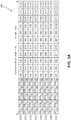
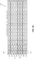
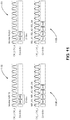
- Figure 3D illustrates a situation where data block 330 has two slots that are the same.
- the data within grouping 332 corresponding to slots DO-D1 are the same; the data within grouping 334 corresponding to slots D2-D3 are the same; the data within grouping 336 corresponding to slots D4-D5 are the same; and the data within grouping 338 corresponding to slots D6-D7 are the same.
- data is sent on data lanes DQ0, DQ2, DQ4, and DQ6 and data lanes DQ1, DQ3, DQ5, and DQ7 are turned off.
- having four active lanes consumes more power than having one or two active lanes, having the four active lanes is still less power consuming than having eight active lanes.
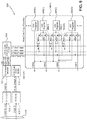
- Separate pattern checking can be used for the data that is being sent over data lanes DQ8-DQ15.
- the modified write command 1106 and the modified read command 1108 are illustrative, and alternate commands could be used.
- the CAS command can be positioned in front of the write or read commands without departing from the scope of the present disclosure.
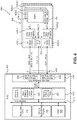
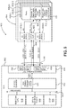
- the host processor 602 may send a normal read command and the memory system 604 uses the backchannel lane 634 to indicate to the host processor 602 that consolidated data is being sent to the host processor 602. While the backchannel lane 634 is illustrated as extending from the command/address/clock block 622, it should be appreciated that other backchannels could be used.
- the backchannel could be an additional DQ lane from a data lane IO block (e.g., data lane IO block 620(1) or 620(2)).
- the CAS command includes a command code and reduced IO per DQ byte (LB-D0, LB-D1 for lower DQ byte (DQ0-DQ7), UB-D0, UB-D1 for upper DQ byte (DQ8-DQ15)).
- LB-D0, LB-D1 for lower DQ byte
- UB-D0, UB-D1 for upper DQ byte
- DQ8-DQ15 DQ8-DQ15
- memory systems interpret a normal write for the lower DQ byte and a reduced IO lane write (WR_X1 for example) for the upper DQ byte.
- Still other truth tables may be constructed to effectuate exemplary aspects of the present disclosure.
- the backchannel lane 634 may be a data mask (DM) lane.
- a DM lane may be associated with the data lane IO blocks 620(1) and 620(2). Normally, if the DM beat is "H," the corresponding DQ byte is not written to the memory array, but traditionally, the DM lane is only used during write commands. Thus, the DM lane is open for use during responses to read commands. In such instance, when a particular DM lane is asserted, that indicates that data consolidation is occurring in response to the read command.
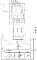
- Figure 14 illustrates an example of a processor-based system 1400 that can employ the host processors 402, 502, and 602 and the memory systems 404, 504, and 604 illustrated in Figures 4-6 .
- the processor-based system 1400 includes one or more CPUs 1402, each including one or more processors 1404, which may be the host processor 402, 502, or 602.
- the CPU(s) 1402 may have cache memory 1406 coupled to the processor(s) 1404 for rapid access to temporarily stored data.
- the CPU(s) 1402 is coupled to a system bus 1408 and can intercouple devices included in the processor-based system 1400.
- the system bus 1408 may be the system bus 414 or 614.
- a processor may also be implemented as a combination of computing devices (e.g., a combination of a DSP and a microprocessor, a plurality of microprocessors, one or more microprocessors in conjunction with a DSP core, or any other such configuration).
- RAM Random Access Memory
- ROM Read Only Memory
- EPROM Electrically Programmable ROM
- EEPROM Electrically Erasable Programmable ROM
- registers a hard disk, a removable disk, a CD-ROM, or any other form of computer readable medium known in the art.
- An exemplary storage medium is coupled to the processor such that the processor can read information from, and write information to, the storage medium.
- the storage medium may be integral to the processor.
- the processor and the storage medium may reside in an ASIC.
- the ASIC may reside in a remote station.
- the processor and the storage medium may reside as discrete components in a remote station, base station, or server.
Landscapes
- Engineering & Computer Science (AREA)
- Theoretical Computer Science (AREA)
- Physics & Mathematics (AREA)
- General Engineering & Computer Science (AREA)
- General Physics & Mathematics (AREA)
- Human Computer Interaction (AREA)
- Techniques For Improving Reliability Of Storages (AREA)
- Memory System (AREA)
- Bus Control (AREA)
- Power Sources (AREA)
Applications Claiming Priority (3)
| Application Number | Priority Date | Filing Date | Title |
|---|---|---|---|
| US201662302891P | 2016-03-03 | 2016-03-03 | |
| US15/448,327 US10222853B2 (en) | 2016-03-03 | 2017-03-02 | Power saving techniques for memory systems by consolidating data in data lanes of a memory bus |
| PCT/US2017/020582 WO2017152005A1 (en) | 2016-03-03 | 2017-03-03 | Power saving techniques for memory systems |
Publications (2)
| Publication Number | Publication Date |
|---|---|
| EP3423947A1 EP3423947A1 (en) | 2019-01-09 |
| EP3423947B1 true EP3423947B1 (en) | 2020-04-22 |
Family
ID=59722700
Family Applications (1)
| Application Number | Title | Priority Date | Filing Date |
|---|---|---|---|
| EP17711926.0A Active EP3423947B1 (en) | 2016-03-03 | 2017-03-03 | Power saving techniques for memory systems |
Country Status (9)
| Country | Link |
|---|---|
| US (2) | US10222853B2 (enExample) |
| EP (1) | EP3423947B1 (enExample) |
| JP (2) | JP6999565B2 (enExample) |
| KR (1) | KR102420909B1 (enExample) |
| CN (1) | CN108701099B (enExample) |
| CA (1) | CA3013090A1 (enExample) |
| ES (1) | ES2804604T3 (enExample) |
| HU (1) | HUE049615T2 (enExample) |
| WO (1) | WO2017152005A1 (enExample) |
Families Citing this family (17)
| Publication number | Priority date | Publication date | Assignee | Title |
|---|---|---|---|---|
| US10222853B2 (en) | 2016-03-03 | 2019-03-05 | Qualcomm Incorporated | Power saving techniques for memory systems by consolidating data in data lanes of a memory bus |
| US10394724B2 (en) * | 2016-08-22 | 2019-08-27 | Qualcomm Incorporated | Low power data transfer for memory subsystem using data pattern checker to determine when to suppress transfers based on specific patterns |
| KR20190035392A (ko) * | 2017-09-26 | 2019-04-03 | 삼성전자주식회사 | 데이터 다중 기록을 수행하는 메모리 장치, 메모리 장치의 동작방법 및 메모리 컨트롤러의 동작방법 |
| KR102731057B1 (ko) * | 2018-09-21 | 2024-11-15 | 삼성전자주식회사 | 메모리 장치와 통신하는 데이터 처리 장치 및 방법 |
| KR20200071396A (ko) * | 2018-12-11 | 2020-06-19 | 에스케이하이닉스 주식회사 | 반도체장치 및 반도체시스템 |
| KR102698036B1 (ko) * | 2019-04-10 | 2024-08-22 | 에스케이하이닉스 주식회사 | 반도체장치 |
| US12061793B1 (en) * | 2020-11-25 | 2024-08-13 | Astera Labs, Inc. | Capacity-expanding memory control component |
| US11722152B1 (en) | 2020-11-25 | 2023-08-08 | Astera Labs, Inc. | Capacity-expanding memory control component |
| KR20220135504A (ko) | 2021-03-30 | 2022-10-07 | 삼성전자주식회사 | 데이터 처리 시스템 및 데이터 처리 장치의 동작 방법 |
| US11785424B1 (en) | 2021-06-28 | 2023-10-10 | Wm Intellectual Property Holdings, L.L.C. | System and method for asset tracking for waste and recycling containers |
| CN116264083B (zh) * | 2021-12-14 | 2025-08-15 | 长鑫存储技术有限公司 | 存储系统以及存储系统的数据读取方法 |
| CN116264085B (zh) * | 2021-12-14 | 2025-08-15 | 长鑫存储技术有限公司 | 存储系统以及存储系统的数据写入方法 |
| US20230197123A1 (en) * | 2021-12-20 | 2023-06-22 | Advanced Micro Devices, Inc. | Method and apparatus for performing a simulated write operation |
| US11899598B2 (en) * | 2022-05-31 | 2024-02-13 | Western Digital Technologies, Inc. | Data storage device and method for lane selection based on thermal conditions |
| KR20240009813A (ko) | 2022-07-14 | 2024-01-23 | 삼성전자주식회사 | 단일 직렬 쓰기 인터페이싱 방식을 지원하는 스토리지 모듈 및 그것의 동작 방법 |
| US12356292B1 (en) | 2023-07-21 | 2025-07-08 | Wm Intellectual Property Holdings, L.L.C. | Apparatus and method for asset tracking for metal waste and recycling containers |
| US12277350B1 (en) | 2023-10-30 | 2025-04-15 | Astera Labs, Inc. | Virtual metadata storage |
Family Cites Families (26)
| Publication number | Priority date | Publication date | Assignee | Title |
|---|---|---|---|---|
| US7190284B1 (en) * | 1994-11-16 | 2007-03-13 | Dye Thomas A | Selective lossless, lossy, or no compression of data based on address range, data type, and/or requesting agent |
| JPH1011360A (ja) * | 1996-06-24 | 1998-01-16 | Toshiba Corp | キャッシュメモリ |
| JP2921505B2 (ja) * | 1996-08-09 | 1999-07-19 | 日本電気株式会社 | 半導体記憶装置 |
| US6009026A (en) * | 1997-07-28 | 1999-12-28 | International Business Machines Corporation | Compressed input/output test mode |
| US6145069A (en) * | 1999-01-29 | 2000-11-07 | Interactive Silicon, Inc. | Parallel decompression and compression system and method for improving storage density and access speed for non-volatile memory and embedded memory devices |
| US6785793B2 (en) | 2001-09-27 | 2004-08-31 | Intel Corporation | Method and apparatus for memory access scheduling to reduce memory access latency |
| US7383399B2 (en) * | 2004-06-30 | 2008-06-03 | Intel Corporation | Method and apparatus for memory compression |
| US7631207B1 (en) * | 2006-04-21 | 2009-12-08 | Sun Microsystems, Inc. | Reducing power consumption for processing of common values in microprocessor registers and execution units |
| GB2457667B (en) | 2008-02-19 | 2012-01-11 | Advanced Risc Mach Ltd | Data transfer between devices within an integrated circuit |
| US8694703B2 (en) * | 2010-06-09 | 2014-04-08 | Brocade Communications Systems, Inc. | Hardware-accelerated lossless data compression |
| RU2556443C2 (ru) | 2010-09-16 | 2015-07-10 | Эппл Инк. | Многопортовый контроллер запоминающего устройства с портами, ассоциированными с классами трафика |
| KR101854251B1 (ko) | 2010-11-30 | 2018-05-03 | 삼성전자주식회사 | 멀티 채널 반도체 메모리 장치 및 그를 구비하는 반도체 장치 |
| US9189394B2 (en) * | 2012-08-08 | 2015-11-17 | Wisconsin Alumni Research Foundation | Memory-link compression for graphic processor unit |
| JP2014053058A (ja) * | 2012-09-06 | 2014-03-20 | Toshiba Corp | 半導体記憶装置 |
| EP2979188A4 (en) | 2013-06-28 | 2016-12-07 | Hewlett Packard Entpr Dev Lp | MEMORY COMPONENT THAT MAY COMMUNICATE TO A PLURALITY OF DATA WIDTHS |
| US9430434B2 (en) | 2013-09-20 | 2016-08-30 | Qualcomm Incorporated | System and method for conserving memory power using dynamic memory I/O resizing |
| US9568542B2 (en) * | 2013-09-25 | 2017-02-14 | Cavium, Inc. | Memory interface with integrated tester |
| US20150121111A1 (en) * | 2013-10-24 | 2015-04-30 | Qualcomm Incorporated | System and method for providing multi-user power saving codebook optmization |
| US9864536B2 (en) * | 2013-10-24 | 2018-01-09 | Qualcomm Incorporated | System and method for conserving power consumption in a memory system |
| US9563251B2 (en) | 2013-12-28 | 2017-02-07 | Intel Corporation | Representing a cache line bit pattern via meta signaling |
| KR102017808B1 (ko) | 2013-12-31 | 2019-09-03 | 에스케이하이닉스 주식회사 | 데이터 처리 장치 및 데이터 처리 방법 |
| CN103714026B (zh) * | 2014-01-14 | 2016-09-28 | 中国人民解放军国防科学技术大学 | 一种支持原址数据交换的存储器访问方法及装置 |
| CA2986559A1 (en) * | 2015-05-21 | 2016-11-24 | Zeropoint Technologies Ab | Methods, devices and systems for semantic-value data compression and decompression |
| US20170115900A1 (en) * | 2015-10-23 | 2017-04-27 | International Business Machines Corporation | Dummy page insertion for flexible page retirement in flash memory storing multiple bits per memory cell |
| US10222853B2 (en) | 2016-03-03 | 2019-03-05 | Qualcomm Incorporated | Power saving techniques for memory systems by consolidating data in data lanes of a memory bus |
| US10394724B2 (en) * | 2016-08-22 | 2019-08-27 | Qualcomm Incorporated | Low power data transfer for memory subsystem using data pattern checker to determine when to suppress transfers based on specific patterns |
-
2017
- 2017-03-02 US US15/448,327 patent/US10222853B2/en active Active
- 2017-03-03 CN CN201780013577.8A patent/CN108701099B/zh active Active
- 2017-03-03 HU HUE17711926A patent/HUE049615T2/hu unknown
- 2017-03-03 WO PCT/US2017/020582 patent/WO2017152005A1/en not_active Ceased
- 2017-03-03 KR KR1020187025182A patent/KR102420909B1/ko active Active
- 2017-03-03 JP JP2018544830A patent/JP6999565B2/ja active Active
- 2017-03-03 CA CA3013090A patent/CA3013090A1/en not_active Abandoned
- 2017-03-03 ES ES17711926T patent/ES2804604T3/es active Active
- 2017-03-03 EP EP17711926.0A patent/EP3423947B1/en active Active
-
2019
- 2019-02-06 US US16/268,634 patent/US10852809B2/en active Active
-
2021
- 2021-12-21 JP JP2021207223A patent/JP7417576B2/ja active Active
Non-Patent Citations (1)
| Title |
|---|
| None * |
Also Published As
| Publication number | Publication date |
|---|---|
| JP2019507436A (ja) | 2019-03-14 |
| US20170255394A1 (en) | 2017-09-07 |
| KR102420909B1 (ko) | 2022-07-13 |
| ES2804604T3 (es) | 2021-02-08 |
| EP3423947A1 (en) | 2019-01-09 |
| KR20180119584A (ko) | 2018-11-02 |
| CN108701099A (zh) | 2018-10-23 |
| US20190179399A1 (en) | 2019-06-13 |
| JP7417576B2 (ja) | 2024-01-18 |
| JP6999565B2 (ja) | 2022-01-18 |
| US10222853B2 (en) | 2019-03-05 |
| CN108701099B (zh) | 2022-05-03 |
| CA3013090A1 (en) | 2017-09-08 |
| HUE049615T2 (hu) | 2020-09-28 |
| WO2017152005A1 (en) | 2017-09-08 |
| US10852809B2 (en) | 2020-12-01 |
| JP2022040150A (ja) | 2022-03-10 |
| BR112018067531A2 (pt) | 2019-01-02 |
Similar Documents
| Publication | Publication Date | Title |
|---|---|---|
| US10852809B2 (en) | Power saving techniques for memory systems by consolidating data in data lanes of a memory bus | |
| KR20130119545A (ko) | 메모리 장치, 메모리 컨트롤러, 메모리 시스템 및 이의 동작 방법 | |
| EP2791809B1 (en) | Unified data masking, data poisoning, and data bus inversion signaling | |
| US10503435B2 (en) | Providing extended dynamic random access memory (DRAM) burst lengths in processor-based systems | |
| KR20190019209A (ko) | Ddr 메모리 에러 복구 | |
| US20140177347A1 (en) | Inter-row data transfer in memory devices | |
| KR20140100690A (ko) | 메모리 장치 및 메모리 장치의 리프레시 방법 | |
| JPH032943A (ja) | 記憶システム | |
| KR102078562B1 (ko) | 리프레쉬 어드레스 생성기 및 이를 포함하는 휘발성 메모리 장치 | |
| KR20160026386A (ko) | 어드레스 정렬기 및 이를 포함하는 메모리 장치 | |
| KR20200055805A (ko) | 다수의 레이턴시 집합을 이용하는 메모리 디바이스 및 이의 작동 방법 | |
| CN111881071B (zh) | 高带宽存储器和系统 | |
| EP4411546B1 (en) | Memory device for synchronizing command start point (csp) | |
| US20180088659A1 (en) | Cache memory clock generation circuits for reducing power consumption and read errors in cache memory | |
| CN118430627A (zh) | 用于同步命令起始点(csp)的存储器设备和方法 | |
| US20240004583A1 (en) | Protocol for data poisoning | |
| CN106940684B (zh) | 一种按比特写数据的方法及装置 | |
| CN119422124A (zh) | 具有伪通道支持的存储器控制器 | |
| BR112018067531B1 (pt) | Processador hospedeiro e sistema de memória | |
| KR20240121652A (ko) | 커맨드 스타트 포인트(csp) 동기화를 위한 메모리 장치 빛 방법 | |
| JPS59191656A (ja) | メモリicシミュレ−タ | |
| KR20160113152A (ko) | 동적 랜덤 액세스 메모리 (dram) 인터페이스들을 위한 직렬 데이터 송신 |
Legal Events
| Date | Code | Title | Description |
|---|---|---|---|
| STAA | Information on the status of an ep patent application or granted ep patent |
Free format text: STATUS: UNKNOWN |
|
| STAA | Information on the status of an ep patent application or granted ep patent |
Free format text: STATUS: THE INTERNATIONAL PUBLICATION HAS BEEN MADE |
|
| PUAI | Public reference made under article 153(3) epc to a published international application that has entered the european phase |
Free format text: ORIGINAL CODE: 0009012 |
|
| STAA | Information on the status of an ep patent application or granted ep patent |
Free format text: STATUS: REQUEST FOR EXAMINATION WAS MADE |
|
| 17P | Request for examination filed |
Effective date: 20180725 |
|
| AK | Designated contracting states |
Kind code of ref document: A1 Designated state(s): AL AT BE BG CH CY CZ DE DK EE ES FI FR GB GR HR HU IE IS IT LI LT LU LV MC MK MT NL NO PL PT RO RS SE SI SK SM TR |
|
| AX | Request for extension of the european patent |
Extension state: BA ME |
|
| DAV | Request for validation of the european patent (deleted) | ||
| DAX | Request for extension of the european patent (deleted) | ||
| GRAP | Despatch of communication of intention to grant a patent |
Free format text: ORIGINAL CODE: EPIDOSNIGR1 |
|
| STAA | Information on the status of an ep patent application or granted ep patent |
Free format text: STATUS: GRANT OF PATENT IS INTENDED |
|
| INTG | Intention to grant announced |
Effective date: 20191106 |
|
| GRAS | Grant fee paid |
Free format text: ORIGINAL CODE: EPIDOSNIGR3 |
|
| GRAA | (expected) grant |
Free format text: ORIGINAL CODE: 0009210 |
|
| STAA | Information on the status of an ep patent application or granted ep patent |
Free format text: STATUS: THE PATENT HAS BEEN GRANTED |
|
| AK | Designated contracting states |
Kind code of ref document: B1 Designated state(s): AL AT BE BG CH CY CZ DE DK EE ES FI FR GB GR HR HU IE IS IT LI LT LU LV MC MK MT NL NO PL PT RO RS SE SI SK SM TR |
|
| REG | Reference to a national code |
Ref country code: CH Ref legal event code: EP |
|
| REG | Reference to a national code |
Ref country code: IE Ref legal event code: FG4D |
|
| REG | Reference to a national code |
Ref country code: DE Ref legal event code: R096 Ref document number: 602017015200 Country of ref document: DE |
|
| REG | Reference to a national code |
Ref country code: AT Ref legal event code: REF Ref document number: 1261034 Country of ref document: AT Kind code of ref document: T Effective date: 20200515 |
|
| REG | Reference to a national code |
Ref country code: CH Ref legal event code: NV Representative=s name: MAUCHER JENKINS PATENTANWAELTE AND RECHTSANWAE, DE |
|
| REG | Reference to a national code |
Ref country code: FI Ref legal event code: FGE |
|
| REG | Reference to a national code |
Ref country code: NL Ref legal event code: FP |
|
| REG | Reference to a national code |
Ref country code: LT Ref legal event code: MG4D |
|
| REG | Reference to a national code |
Ref country code: HU Ref legal event code: AG4A Ref document number: E049615 Country of ref document: HU |
|
| PG25 | Lapsed in a contracting state [announced via postgrant information from national office to epo] |
Ref country code: NO Free format text: LAPSE BECAUSE OF FAILURE TO SUBMIT A TRANSLATION OF THE DESCRIPTION OR TO PAY THE FEE WITHIN THE PRESCRIBED TIME-LIMIT Effective date: 20200722 Ref country code: GR Free format text: LAPSE BECAUSE OF FAILURE TO SUBMIT A TRANSLATION OF THE DESCRIPTION OR TO PAY THE FEE WITHIN THE PRESCRIBED TIME-LIMIT Effective date: 20200723 Ref country code: IS Free format text: LAPSE BECAUSE OF FAILURE TO SUBMIT A TRANSLATION OF THE DESCRIPTION OR TO PAY THE FEE WITHIN THE PRESCRIBED TIME-LIMIT Effective date: 20200822 Ref country code: SE Free format text: LAPSE BECAUSE OF FAILURE TO SUBMIT A TRANSLATION OF THE DESCRIPTION OR TO PAY THE FEE WITHIN THE PRESCRIBED TIME-LIMIT Effective date: 20200422 Ref country code: PT Free format text: LAPSE BECAUSE OF FAILURE TO SUBMIT A TRANSLATION OF THE DESCRIPTION OR TO PAY THE FEE WITHIN THE PRESCRIBED TIME-LIMIT Effective date: 20200824 Ref country code: LT Free format text: LAPSE BECAUSE OF FAILURE TO SUBMIT A TRANSLATION OF THE DESCRIPTION OR TO PAY THE FEE WITHIN THE PRESCRIBED TIME-LIMIT Effective date: 20200422 |
|
| REG | Reference to a national code |
Ref country code: AT Ref legal event code: MK05 Ref document number: 1261034 Country of ref document: AT Kind code of ref document: T Effective date: 20200422 |
|
| PG25 | Lapsed in a contracting state [announced via postgrant information from national office to epo] |
Ref country code: BG Free format text: LAPSE BECAUSE OF FAILURE TO SUBMIT A TRANSLATION OF THE DESCRIPTION OR TO PAY THE FEE WITHIN THE PRESCRIBED TIME-LIMIT Effective date: 20200722 Ref country code: LV Free format text: LAPSE BECAUSE OF FAILURE TO SUBMIT A TRANSLATION OF THE DESCRIPTION OR TO PAY THE FEE WITHIN THE PRESCRIBED TIME-LIMIT Effective date: 20200422 Ref country code: RS Free format text: LAPSE BECAUSE OF FAILURE TO SUBMIT A TRANSLATION OF THE DESCRIPTION OR TO PAY THE FEE WITHIN THE PRESCRIBED TIME-LIMIT Effective date: 20200422 Ref country code: HR Free format text: LAPSE BECAUSE OF FAILURE TO SUBMIT A TRANSLATION OF THE DESCRIPTION OR TO PAY THE FEE WITHIN THE PRESCRIBED TIME-LIMIT Effective date: 20200422 |
|
| PG25 | Lapsed in a contracting state [announced via postgrant information from national office to epo] |
Ref country code: AL Free format text: LAPSE BECAUSE OF FAILURE TO SUBMIT A TRANSLATION OF THE DESCRIPTION OR TO PAY THE FEE WITHIN THE PRESCRIBED TIME-LIMIT Effective date: 20200422 |
|
| REG | Reference to a national code |
Ref country code: DE Ref legal event code: R097 Ref document number: 602017015200 Country of ref document: DE |
|
| PG25 | Lapsed in a contracting state [announced via postgrant information from national office to epo] |
Ref country code: EE Free format text: LAPSE BECAUSE OF FAILURE TO SUBMIT A TRANSLATION OF THE DESCRIPTION OR TO PAY THE FEE WITHIN THE PRESCRIBED TIME-LIMIT Effective date: 20200422 Ref country code: DK Free format text: LAPSE BECAUSE OF FAILURE TO SUBMIT A TRANSLATION OF THE DESCRIPTION OR TO PAY THE FEE WITHIN THE PRESCRIBED TIME-LIMIT Effective date: 20200422 Ref country code: AT Free format text: LAPSE BECAUSE OF FAILURE TO SUBMIT A TRANSLATION OF THE DESCRIPTION OR TO PAY THE FEE WITHIN THE PRESCRIBED TIME-LIMIT Effective date: 20200422 Ref country code: SM Free format text: LAPSE BECAUSE OF FAILURE TO SUBMIT A TRANSLATION OF THE DESCRIPTION OR TO PAY THE FEE WITHIN THE PRESCRIBED TIME-LIMIT Effective date: 20200422 Ref country code: IT Free format text: LAPSE BECAUSE OF FAILURE TO SUBMIT A TRANSLATION OF THE DESCRIPTION OR TO PAY THE FEE WITHIN THE PRESCRIBED TIME-LIMIT Effective date: 20200422 Ref country code: CZ Free format text: LAPSE BECAUSE OF FAILURE TO SUBMIT A TRANSLATION OF THE DESCRIPTION OR TO PAY THE FEE WITHIN THE PRESCRIBED TIME-LIMIT Effective date: 20200422 Ref country code: RO Free format text: LAPSE BECAUSE OF FAILURE TO SUBMIT A TRANSLATION OF THE DESCRIPTION OR TO PAY THE FEE WITHIN THE PRESCRIBED TIME-LIMIT Effective date: 20200422 |
|
| REG | Reference to a national code |
Ref country code: ES Ref legal event code: FG2A Ref document number: 2804604 Country of ref document: ES Kind code of ref document: T3 Effective date: 20210208 |
|
| PG25 | Lapsed in a contracting state [announced via postgrant information from national office to epo] |
Ref country code: PL Free format text: LAPSE BECAUSE OF FAILURE TO SUBMIT A TRANSLATION OF THE DESCRIPTION OR TO PAY THE FEE WITHIN THE PRESCRIBED TIME-LIMIT Effective date: 20200422 Ref country code: SK Free format text: LAPSE BECAUSE OF FAILURE TO SUBMIT A TRANSLATION OF THE DESCRIPTION OR TO PAY THE FEE WITHIN THE PRESCRIBED TIME-LIMIT Effective date: 20200422 |
|
| PLBE | No opposition filed within time limit |
Free format text: ORIGINAL CODE: 0009261 |
|
| STAA | Information on the status of an ep patent application or granted ep patent |
Free format text: STATUS: NO OPPOSITION FILED WITHIN TIME LIMIT |
|
| 26N | No opposition filed |
Effective date: 20210125 |
|
| PG25 | Lapsed in a contracting state [announced via postgrant information from national office to epo] |
Ref country code: SI Free format text: LAPSE BECAUSE OF FAILURE TO SUBMIT A TRANSLATION OF THE DESCRIPTION OR TO PAY THE FEE WITHIN THE PRESCRIBED TIME-LIMIT Effective date: 20200422 |
|
| PG25 | Lapsed in a contracting state [announced via postgrant information from national office to epo] |
Ref country code: MC Free format text: LAPSE BECAUSE OF FAILURE TO SUBMIT A TRANSLATION OF THE DESCRIPTION OR TO PAY THE FEE WITHIN THE PRESCRIBED TIME-LIMIT Effective date: 20200422 |
|
| REG | Reference to a national code |
Ref country code: BE Ref legal event code: MM Effective date: 20210331 |
|
| PG25 | Lapsed in a contracting state [announced via postgrant information from national office to epo] |
Ref country code: LU Free format text: LAPSE BECAUSE OF NON-PAYMENT OF DUE FEES Effective date: 20210303 Ref country code: IE Free format text: LAPSE BECAUSE OF NON-PAYMENT OF DUE FEES Effective date: 20210303 |
|
| PG25 | Lapsed in a contracting state [announced via postgrant information from national office to epo] |
Ref country code: BE Free format text: LAPSE BECAUSE OF NON-PAYMENT OF DUE FEES Effective date: 20210331 |
|
| PG25 | Lapsed in a contracting state [announced via postgrant information from national office to epo] |
Ref country code: CY Free format text: LAPSE BECAUSE OF FAILURE TO SUBMIT A TRANSLATION OF THE DESCRIPTION OR TO PAY THE FEE WITHIN THE PRESCRIBED TIME-LIMIT Effective date: 20200422 |
|
| PG25 | Lapsed in a contracting state [announced via postgrant information from national office to epo] |
Ref country code: MK Free format text: LAPSE BECAUSE OF FAILURE TO SUBMIT A TRANSLATION OF THE DESCRIPTION OR TO PAY THE FEE WITHIN THE PRESCRIBED TIME-LIMIT Effective date: 20200422 |
|
| PG25 | Lapsed in a contracting state [announced via postgrant information from national office to epo] |
Ref country code: TR Free format text: LAPSE BECAUSE OF FAILURE TO SUBMIT A TRANSLATION OF THE DESCRIPTION OR TO PAY THE FEE WITHIN THE PRESCRIBED TIME-LIMIT Effective date: 20200422 |
|
| PG25 | Lapsed in a contracting state [announced via postgrant information from national office to epo] |
Ref country code: MT Free format text: LAPSE BECAUSE OF FAILURE TO SUBMIT A TRANSLATION OF THE DESCRIPTION OR TO PAY THE FEE WITHIN THE PRESCRIBED TIME-LIMIT Effective date: 20200422 |
|
| PGFP | Annual fee paid to national office [announced via postgrant information from national office to epo] |
Ref country code: NL Payment date: 20250212 Year of fee payment: 9 |
|
| PGFP | Annual fee paid to national office [announced via postgrant information from national office to epo] |
Ref country code: DE Payment date: 20250210 Year of fee payment: 9 |
|
| PGFP | Annual fee paid to national office [announced via postgrant information from national office to epo] |
Ref country code: FI Payment date: 20250225 Year of fee payment: 9 |
|
| PGFP | Annual fee paid to national office [announced via postgrant information from national office to epo] |
Ref country code: HU Payment date: 20250303 Year of fee payment: 9 |
|
| PGFP | Annual fee paid to national office [announced via postgrant information from national office to epo] |
Ref country code: FR Payment date: 20250210 Year of fee payment: 9 |
|
| PGFP | Annual fee paid to national office [announced via postgrant information from national office to epo] |
Ref country code: GB Payment date: 20250213 Year of fee payment: 9 |
|
| PGFP | Annual fee paid to national office [announced via postgrant information from national office to epo] |
Ref country code: ES Payment date: 20250409 Year of fee payment: 9 |
|
| PGFP | Annual fee paid to national office [announced via postgrant information from national office to epo] |
Ref country code: CH Payment date: 20250401 Year of fee payment: 9 |