EP3407100B1 - Nd-filter mit kunststoff-grundmaterial und nd-filter mit kunststoff-grundmaterial für brillen - Google Patents
Nd-filter mit kunststoff-grundmaterial und nd-filter mit kunststoff-grundmaterial für brillen Download PDFInfo
- Publication number
- EP3407100B1 EP3407100B1 EP17756349.1A EP17756349A EP3407100B1 EP 3407100 B1 EP3407100 B1 EP 3407100B1 EP 17756349 A EP17756349 A EP 17756349A EP 3407100 B1 EP3407100 B1 EP 3407100B1
- Authority
- EP
- European Patent Office
- Prior art keywords
- layer
- film
- base
- sio
- nio
- Prior art date
- Legal status (The legal status is an assumption and is not a legal conclusion. Google has not performed a legal analysis and makes no representation as to the accuracy of the status listed.)
- Active
Links
Images


Classifications
-
- G—PHYSICS
- G02—OPTICS
- G02B—OPTICAL ELEMENTS, SYSTEMS OR APPARATUS
- G02B5/00—Optical elements other than lenses
- G02B5/20—Filters
- G02B5/205—Neutral density filters
-
- B—PERFORMING OPERATIONS; TRANSPORTING
- B32—LAYERED PRODUCTS
- B32B—LAYERED PRODUCTS, i.e. PRODUCTS BUILT-UP OF STRATA OF FLAT OR NON-FLAT, e.g. CELLULAR OR HONEYCOMB, FORM
- B32B27/00—Layered products comprising a layer of synthetic resin
- B32B27/06—Layered products comprising a layer of synthetic resin as the main or only constituent of a layer, which is next to another layer of the same or of a different material
- B32B27/08—Layered products comprising a layer of synthetic resin as the main or only constituent of a layer, which is next to another layer of the same or of a different material of synthetic resin
-
- B—PERFORMING OPERATIONS; TRANSPORTING
- B32—LAYERED PRODUCTS
- B32B—LAYERED PRODUCTS, i.e. PRODUCTS BUILT-UP OF STRATA OF FLAT OR NON-FLAT, e.g. CELLULAR OR HONEYCOMB, FORM
- B32B27/00—Layered products comprising a layer of synthetic resin
- B32B27/28—Layered products comprising a layer of synthetic resin comprising synthetic resins not wholly covered by any one of the sub-groups B32B27/30 - B32B27/42
-
- B—PERFORMING OPERATIONS; TRANSPORTING
- B32—LAYERED PRODUCTS
- B32B—LAYERED PRODUCTS, i.e. PRODUCTS BUILT-UP OF STRATA OF FLAT OR NON-FLAT, e.g. CELLULAR OR HONEYCOMB, FORM
- B32B27/00—Layered products comprising a layer of synthetic resin
- B32B27/40—Layered products comprising a layer of synthetic resin comprising polyurethanes
-
- B—PERFORMING OPERATIONS; TRANSPORTING
- B32—LAYERED PRODUCTS
- B32B—LAYERED PRODUCTS, i.e. PRODUCTS BUILT-UP OF STRATA OF FLAT OR NON-FLAT, e.g. CELLULAR OR HONEYCOMB, FORM
- B32B7/00—Layered products characterised by the relation between layers; Layered products characterised by the relative orientation of features between layers, or by the relative values of a measurable parameter between layers, i.e. products comprising layers having different physical, chemical or physicochemical properties; Layered products characterised by the interconnection of layers
- B32B7/02—Physical, chemical or physicochemical properties
- B32B7/023—Optical properties
-
- B—PERFORMING OPERATIONS; TRANSPORTING
- B32—LAYERED PRODUCTS
- B32B—LAYERED PRODUCTS, i.e. PRODUCTS BUILT-UP OF STRATA OF FLAT OR NON-FLAT, e.g. CELLULAR OR HONEYCOMB, FORM
- B32B9/00—Layered products comprising a layer of a particular substance not covered by groups B32B11/00 - B32B29/00
-
- G—PHYSICS
- G02—OPTICS
- G02B—OPTICAL ELEMENTS, SYSTEMS OR APPARATUS
- G02B1/00—Optical elements characterised by the material of which they are made; Optical coatings for optical elements
- G02B1/10—Optical coatings produced by application to, or surface treatment of, optical elements
- G02B1/11—Anti-reflection coatings
- G02B1/113—Anti-reflection coatings using inorganic layer materials only
- G02B1/115—Multilayers
-
- G—PHYSICS
- G02—OPTICS
- G02B—OPTICAL ELEMENTS, SYSTEMS OR APPARATUS
- G02B1/00—Optical elements characterised by the material of which they are made; Optical coatings for optical elements
- G02B1/10—Optical coatings produced by application to, or surface treatment of, optical elements
- G02B1/14—Protective coatings, e.g. hard coatings
-
- G—PHYSICS
- G02—OPTICS
- G02B—OPTICAL ELEMENTS, SYSTEMS OR APPARATUS
- G02B5/00—Optical elements other than lenses
-
- G—PHYSICS
- G02—OPTICS
- G02C—SPECTACLES; SUNGLASSES OR GOGGLES INSOFAR AS THEY HAVE THE SAME FEATURES AS SPECTACLES; CONTACT LENSES
- G02C7/00—Optical parts
- G02C7/10—Filters, e.g. for facilitating adaptation of the eyes to the dark; Sunglasses
-
- G—PHYSICS
- G02—OPTICS
- G02C—SPECTACLES; SUNGLASSES OR GOGGLES INSOFAR AS THEY HAVE THE SAME FEATURES AS SPECTACLES; CONTACT LENSES
- G02C7/00—Optical parts
- G02C7/10—Filters, e.g. for facilitating adaptation of the eyes to the dark; Sunglasses
- G02C7/107—Interference colour filters
-
- B—PERFORMING OPERATIONS; TRANSPORTING
- B32—LAYERED PRODUCTS
- B32B—LAYERED PRODUCTS, i.e. PRODUCTS BUILT-UP OF STRATA OF FLAT OR NON-FLAT, e.g. CELLULAR OR HONEYCOMB, FORM
- B32B2255/00—Coating on the layer surface
- B32B2255/10—Coating on the layer surface on synthetic resin layer or on natural or synthetic rubber layer
-
- B—PERFORMING OPERATIONS; TRANSPORTING
- B32—LAYERED PRODUCTS
- B32B—LAYERED PRODUCTS, i.e. PRODUCTS BUILT-UP OF STRATA OF FLAT OR NON-FLAT, e.g. CELLULAR OR HONEYCOMB, FORM
- B32B2255/00—Coating on the layer surface
- B32B2255/20—Inorganic coating
-
- B—PERFORMING OPERATIONS; TRANSPORTING
- B32—LAYERED PRODUCTS
- B32B—LAYERED PRODUCTS, i.e. PRODUCTS BUILT-UP OF STRATA OF FLAT OR NON-FLAT, e.g. CELLULAR OR HONEYCOMB, FORM
- B32B2551/00—Optical elements
Definitions
- the present invention relates to a ND (Neutral Density) filter with a plastic base, and a ND filter with a plastic base for eyeglasses.
- ND Neutral Density
- the ND filter disclosed in JP 5066644 B2 is known.
- the ND filter has a structure in which a plurality of light absorbing films and a plurality of dielectric films are layered and formed on one or both surfaces of a transparent substrate, and the light absorbing film contains elemental germanium or elemental silicon and a mixture (Ni+NiO x ) of nickel and an oxide of nickel.
- US 2006/018050 A1 discloses a ND filter according to the preamble of claim 1.
- the substrate is formed from reinforced glass or plastic.
- a plastic substrate is preferable, and is preferable, in particular, for spectacles.
- JP 5066644 B2 does not particularly describe moisture from the plastic substrate, and there is room for further improving lifespan such as weather resistance in the technique disclosed in JP 5066644 B2 (plastic substrate).
- an object of the invention described in claims 1 and 8 is to provide a ND filter and a ND filter, for spectacles, each of which has a base (substrate) formed from plastic, and has an excellent durability.
- an effect of providing a neutral density filter and a neutral density filter, for eyeglasses, each of which has a base formed from plastic and has an excellent durability, can be obtained.
- AND filter according to the present invention is a filter that uniformly absorbs at least light (visible light) having a wavelength in a visible region (for example, not less than 400 nanometers (nm) and not greater than 800 nm, not less than 400 nm and not greater than 760 nm, not less than 400 nm and not greater than 700 nm, not less than 410 nm and not greater than 760 nm, or not less than 420 nm and not greater than 760 nm).
- a visible region for example, not less than 400 nanometers (nm) and not greater than 800 nm, not less than 400 nm and not greater than 760 nm, not less than 400 nm and not greater than 700 nm, not less than 410 nm and not greater than 760 nm, or not less than 420 nm and not greater than 760 nm).
- a base of the ND filter is formed from a transparent (including translucent as appropriate) plastic.
- a material of the base include polyurethane resin, protecting another lens or incorporated in a camera body) or similarly used for projectors, binoculars, and telescopes, and more preferably used for spectacles (used as a spectacles lens itself or used as a lens for covering a spectacles lens).
- An optical multilayer film is formed on one surface or both surfaces of the base.
- the optical multilayer film mainly has a function of uniformly absorbing visible light, and further has a function of preventing reflection of the visible light as appropriate.
- the optical multilayer film or a portion thereof for absorbing visible light is a light absorbing film.
- the light absorbing film may be a light absorbing layer.
- the optical multilayer film or a portion thereof for preventing reflection of visible light is an antireflection film.
- the antireflection film may include a light absorbing film.
- both the optical multilayer films may have the same structure, or may have different structures.
- the optical multilayer film may be formed from a light absorbing film only.
- the optical multilayer film may have an antifouling film or a protective film added on the front surface side (air side) of the light absorbing film.
- the optical multilayer film may have a single or a plurality of intermediate layers, such as a hard coating film, which is added on the base side of the light absorbing film.
- the optical multilayer film may have a single or a plurality of layers or films added inside or outside the light absorbing film, for another purpose such as improvement of conductivity.
- the optical multilayer film may be obtained by combination of above-described layers and/or films.
- a hard coating film, a conductive layer, an antireflection film, or the like may not be included in the optical multilayer film. Each of them or a combination thereof may be formed as a separate optical multilayer film.
- the hard coating film is formed from, for example, an organosiloxane compound, or is formed from an organosilicon compound or an acrylic compound.
- a primer layer may be formed.
- the primer layer is formed from, for example, at least one of polyurethane-based resin, acrylic resin, methacrylic resin, and organosilicon resin.
- the antireflection film is formed from, for example, a plurality of kinds of dielectric materials including a low refractive index material and a high refractive index material.
- a low refractive index material for example, at least one of silicon oxide (in particular, SiO 2 ) and magnesium fluoride (in particular, MgF 2 ) is used.
- MgF 2 magnesium fluoride
- the high refractive index material for example, at least one of zirconium oxide (in particular, ZrO 2 ), titanium oxide (in particular, TiO 2 ), tantalum oxide (in particular, Ta 2 O 5 ), and niobium oxide (in particular, Nb 2 O 5 ) is used.
- the antireflection film is preferably formed such that the low refractive index materials and the high refractive index materials are alternately layered by one of the low and the high refractive index materials being positioned on the base side.
- the light absorbing film is formed so as to include one or more light absorbing layers formed from at least one unsaturated oxide of nickel (Ni) and cobalt (Co), as defined by the independent claim.
- NiO x an unsaturated metal oxide film
- x is greater than 0 and not greater than 1
- Ni is a deposition material and deposited in a state where oxygen gas is supplied into a deposition vacuum device at a predetermined flow rate, whereby the value of x can be adjusted.
- CoO x' an unsaturated metal oxide film
- x' is greater than 0 and not greater than 1.5
- Co is a deposition material and deposited in a state where oxygen gas is supplied into a deposition vacuum device at a predetermined flow rate, whereby the value of x'can be adjusted.
- the light absorbing film may be formed as a multilayer film having another layer.
- the other layer include a SiO 2 layer, a ZrO 2 layer, an aluminium oxide (in particular, Al 2 O 3 ) layer, a silica compound layer, and a combination thereof.
- the silica compound is a silicon compound or a mixture of a silicon compound and another compound.
- the silica compound is preferably a mixture of silicon oxide and aluminium oxide, and is more preferably a mixture of SiO 2 and Al 2 O 3 .
- an adjacent layer, on the base side, of the at least one light absorbing layer and an adjacent layer thereof on the opposite side (air side) are formed from different materials, respectively.
- the adjacent layer on the base side is an Al 2 O 3 layer
- the adjacent layer on the opposite side is a silica compound layer.
- the adjacent layer, on the base side, of at least one of the NiO x layers and the adjacent layer thereof on the opposite side may be formed from different materials, respectively.
- the adjacent layer, on the base side, of at least one of the CoO x' layers and the adjacent layer thereof on the opposite side may be formed from different materials, respectively.
- the adjacent layer, on the base side, of at least one of the NiO x layer and the CoO x' layer and the adjacent layer thereof on the opposite side may be formed from different materials, respectively.
- the adjacent layer, on the base side, of one of the NiO x layers and the CoO x' layers and the adjacent layer thereof on the opposite side may be formed from different materials, respectively.
- the adjacent layer on the base side or the adjacent layer on the opposite side is preferably a silica compound layer because the silica compound layer has a density which allows less moisture permeation as compared to a density of the ZrO 2 layer, does not have an ultra-high density that allows moisture to be completely sealed, and has an appropriate moisture permeation degree.
- the first layer (initial layer) from the base side of the light absorbing film is a SiO 2 layer or an Al 2 O 3 layer.
- the initial layer of the light absorbing film preferably has a density as obtained without performing ion-assisted deposition.
- the density of the deposited film such as the initial layer is very difficult to directly measure for a person skilled in the art. Specifying a degree of a density of the deposited film according to whether or not ion assisted deposition is performed is easy and useful for a person skilled in the art.
- the light absorbing film may also have a function as an antireflection film in addition to a light absorbing function by low refractive index layers and high refractive index layers being alternately disposed.
- the NiO x layer and the CoO x' layer may be handled as the high refractive index layers.
- the base preferably has front and back surfaces as a base for spectacles and the like.
- the front surface of the ND filter base for spectacles is on an environment side, and the back surface thereof is on a face side.
- the antireflection film is preferably disposed on the front surface side of the base, and the light absorbing film is preferably disposed on the back surface side thereof.
- the antireflection film has a higher durability than the light absorbing film.
- the antireflection film having a relatively high durability is disposed on the front surface that is exposed to harsher environment, and the light absorbing film is disposed on the back surface that is protected relatively well.
- light absorption (ND) and antireflection functions are assured, and durability can be improved as a whole while advantageous properties are obtained.
- This ND filter is advantageously used for spectacles. That is, the ND filter itself may be used as a spectacles lens, and the ND filter may be prepared as a filter that covers another spectacles lens.
- the ND filter, for spectacles, according to the present invention uniformly absorbs visible light in a visible region and can thus provide visibility equivalent to that by naked eyes.
- convex lenses, for spectacles each having a round shape and having the diameter of 75 millimeters (mm) were produced.
- the power was S-4.00
- the shape on the convex surface side (front surface side) was non-spherical
- the thickness was 1.2 mm at the center.
- Each of the bases was formed from episulfide resin, and had a refractive index of 1.76, the Abbe number of 30, and the specific gravity of 1.49 g/cm 3 (gram per cubic centimeter).
- HC films On both the front and back surfaces of the base, hard coating films (HC films) were formed.
- the hard coating films were formed by the same hard coating solution being applied in the same manner.
- the hard coating solution was produced as follows. Firstly, 206 g (gram) of methanol, 300g of a methanol-dispersed titania sol (made by JGC Catalysts and Chemicals Ltd., solid content was 30%), 30g of ⁇ -glycidoxypropylmethyldiethoxysilane, and 60 g of tetraethoxysilane were dropped in a container, and 0.01 N (normality) of hydrochloric acid aqueous solution was dropped into the mixed solution. The resultant mixed solution was stirred and hydrolyzed. Next, 0.5 g of flow regulating agent and 1.0 g of catalyst were added, and the resultant solution was stirred at room temperature for three hours, to obtain the hard coating solution.
- the hard coating solution was uniformly applied to the surface of the base by a spin coating method, and was then left as it was in an environment of 120°C for 1.5 hours, whereby the hard coating solution was heat-cured, to obtain the hard coating film.
- the physical film thickness of the hard coating film having been thus formed was 2.5 ⁇ m (micrometer).
- an antireflection film (AR film) and a water-repellent layer were formed on the convex surface (front surface) side of the base.
- the base having the hard coating film was set in a fixing tool (dome), and was put into a vacuum device through a door. Thereafter, the door was closed, and the vacuum device was evacuated. The temperature in the vacuum device was maintained at 60°C in order to remove moisture from the base.
- the degree of vacuum in the vacuum device was 1.0E-03 (1.0 ⁇ 10 -3 ) Pa (pascal)
- the following film formation was started. That is, firstly, the surface of the base was activated by applying oxygen ions to the surface of the base for 60 seconds in order to enhance adhesion between the intermediate layer (hard coating film) and the optical multilayer film to be then formed.
- SiO 2 for a low refractive index material and ZrO 2 for a high refractive index material were alternately deposited such that each material was deposited for a predetermined time, and five layers of the antireflection film were formed in total on the convex surface of the base such that each layer had a desired film thickness.
- a water repellent agent was deposited on the convex surface side of the base having the antireflection film, and the water-repellent layer (top layer) was formed on the antireflection film.
- the structures of the optical multilayer films on the convex surface side according to examples 1 to 8 and comparative example 1 to 7 are as indicated below in Table 1. Unless otherwise specified, the film thickness is a physical film thickness. [Table 1] Examples 1 to 8, Comparative examples 1 to 7 Base ⁇ HC film side Material and the like Film thickness [nm] AR film-formed convex surface First layer SiO 2 80 Second layer ZrO 2 29 Third layer SiO 2 31 Fourth layer ZrO 2 58 Fifth layer SiO 2 92 Water-repellent layer ---
- the light absorbing film and the water-repellent layer were formed on the concave surface (back surface) side of the base.
- the light absorbing film was formed, similarly to formation of the antireflection film, by adjusting conditions at the start of the film formation.
- the film was formed, after oxygen ions were similarly applied, the following materials were formed into films under the following conditions.
- ions were not applied except for the initial oxygen ion application, and the light absorbing film was deposited without ion-assisting (non-Ion Assist Deposition).
- the weight of SiO 2 is greater than the weight of Al 2 O 3 , and, for example, a percentage of the weight of Al 2 O 3 relative to the weight of SiO 2 is about several %.
- the percentage of the weight of Al 2 O 3 to the weight of SiO 2 is not particularly limited, and the component of the silica compound is not limited to SiO 2 and Al 2 O 3 .
- the water-repellent layer was formed on the light absorbing film (air side) similarly to one on the antireflection film.
- Example 1 Example 2
- Example 3 Example 4 Material and the like Film thickness [nm] Material and the like Film thickness [nm] Material and the like Film thickness [nm] Material and the like Film thickness [nm] Material and the like Film thickness [nm] - base --- base --- base --- base --- - HC film --- HC film --- HC film --- HC film --- 1 SiO 2 40.0 SiO 2 40.0 SiO 2 70.0 Al 2 O 3 30.0 2 Al 2 O 3 40.0 Al 2 O 3 30.0 Al 2 O 3 30.0 Al 2 O 3 30.0 NiO X 4.2 3 NiO x 4.4 NiO x 4.5 NiO X 4.2 SiO 2 +Al 2 O 3 35.0 4 SiO 2 +Al 2 O 3 30.0 Al 2 O 3 30.0 Al 2 O 3 45.0 NiO X 4.2 5 NiO x 4.4 NiO x 4.5 NiO X 4.2
- a PET (polyethylene terephthalate) film was a base.
- a water vapor permeability (gram per cubic meter for one day, g/m 2 ⁇ day) was measured for a case where only a base was used, and for a case where a SiO 2 film, an Al 2 O 3 film, or a SiO 2 +Al 2 O 3 -mixture film was deposited on the base by changing between use of ion-assisting and non-use thereof.
- the water vapor permeability was 7.29.
- the SiO 2 film, the Al 2 O 3 film, or the SiO 2 +Al 2 O 3 -mixture film (deposition materials are described in the column for "material” in Table 6) was deposited without ion-assisting such that the film thicknesses were 90.3 nm, 94.8 nm, 74.4 nm, the water vapor permeabilities were 6.75, 6.28, 6.12, and were slightly lower than that in the case where only the base was used. This is because the SiO 2 film, the Al 2 O 3 film, or the SiO 2 +Al 2 O 3 -mixture film prevented permeation of water vapor.
- the SiO 2 film was deposited by ion-assisting (acceleration voltage of 900 volts (V), acceleration current of 900 milliampere (mA), bias current of 600 mA, and introduced oxygen (O 2 ) gas at 50 sccm, by means of an ion gun) such that the film thickness was 69.1 nm, the water vapor permeability was 3.77 and was thus more greatly reduced.
- ion-assisting acceleration voltage of 900 volts (V)
- acceleration current of 900 milliampere (mA) acceleration current of 900 milliampere
- bias current 600 mA
- O 2 oxygen
- the Al 2 O 3 film was deposited by ion-assisting (acceleration voltage of 1000 V, acceleration current of 1000 mA, bias current of 600 mA, and introduced oxygen gas at 50 sccm) such that the film thickness was 79.0 nm, the water vapor permeability was 0.89 and was thus greatly reduced.
- the density of the Al 2 O 3 film formed by ion-assisted deposition was greater than the density in the case of ion-assisting being not performed, and the Al 2 O 3 film having such a great density further prevented permeation of water vapor.
- the Si0 2 +A1 2 0 3 -mixture film was similarly deposited by performing ion-assisting similar to the SiO 2 film such that the film thickness was 75.0 nm, the water vapor permeability was 1.61 and was thus low.
- the density of the SiO 2 +Al 2 O 3 -mixture film formed by ion-assisted deposition was greater than the density in the case of ion-assisting being not performed, and the SiO 2 +Al 2 O 3 -mixture film having such a great density further prevented permeation of water vapor.
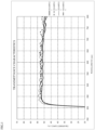
- FIG. 1 shows a graph representing a spectral transmittance distribution in a visible region according to examples 1 to 4.
- the spectral transmittance distribution was measured by using a spectrophotometer (U-4100 manufactured by Hitachi High-Technologies Corporation).
- the transmittance in a visible region was 51 ⁇ 3% so as to be within a band-shaped region and visible light was uniformly absorbed at an absorption rate of about 50%
- the ND filter, for spectacles which prevented a color recognized during wearing from being greatly different from a color by naked eyes while having gray outer appearance, was able to be obtained.
- the absorption rate in the uniform absorption can be variously changed.
- Table 7 indicates values of L, a, and b in Lab color space (UCS space) according to examples 1 to 8 as follows. These values were measured by using a D65 light source at a viewing angle of 2°.
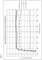
- FIG. 2 shows a graph representing a spectral transmittance distribution in a visible region according to examples 5 to 8.
- Example 5 (NiO x layer) and example 6 (CoO x' layer) each indicated a spectral transmittance distribution similar to those of examples 1 to 4 and had values of L, a, and b similar to those of examples 1 to 4. That is, in examples 5 and 6, the transmittance in a visible region was 54 ⁇ 3% so as to be within a band-shaped region and visible light was uniformly absorbed at an absorption rate of about 46%, and the ND filter, for spectacles, which prevented a color recognized during wearing from being greatly different from a color by naked eyes while having gray outer appearance, was able to be obtained. Furthermore, comparison between examples 5 and 6 indicates that the NiO x layer and the CoO x' layer have similar characteristics and can be similarly used.
- the number of the light absorbing layers was increased to three although the number thereof in each of examples 1 to 5 was two. Therefore, the absorption rate of visible light was higher than those of examples 1 to 5.
- the transmittance in a visible region was 31 ⁇ 2% so as to be within a band-shaped region and visible light was uniformly absorbed at an absorption rate of about 70%, and the ND filter, for spectacles, which prevented a color recognized during wearing from being greatly different from a color by naked eyes while having gray outer appearance, was able to be obtained.
- Example 7 indicated values of a and b which were similar to those of examples 1 to 6, and the L value which was reduced as compared to examples 1 to 6.
- both the NiO x layer and the CoO x' layer were used as the light absorbing layer.
- the transmittance in a visible region was 47 ⁇ 2% so as to be within a band-shaped region and visible light was uniformly absorbed at an absorption rate of about 53%
- the ND filter, for spectacles which prevented a color recognized during wearing from being greatly different from a color by naked eyes while having gray outer appearance, was able to be obtained.
- Example 8 indicated values of a and b which were similar to those of examples 1 to 6, and the L value which was slightly reduced as compared to examples 1 to 6.
- FIG. 3 shows a graph representing a spectral transmittance distribution for a dyed spectacles lens which is commercially available as gray sunglasses (concentration of 50%).
- the dyed spectacles lens had gray color similar to examples 1 to 8, and a lot of extreme values in a range of 45% to 94% were indicated in the spectral transmittance distribution in a visible region. Color during wearing was greatly different from color by naked eyes.
- Example 1 Example 2
- Example 3 Example 4 Lab space L 73.56 72.31 72.52 72.45 a -4.34 -4.24 -4.29 -4.49 b 2.76 4.61 3.62 4.67
- Example 5 Example 6
- Example 7 Example 8 Lab space L 73.04 71.97 54.73 69.31 a -3.48 -4.21 -2.18 -4.17 b 4.57 5.58 2.28 4.87
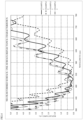
- FIG. 4 shows a graph representing a spectral reflectance distribution (one surface) in a visible region on the concave surface (ND-film formed surface) side according to examples 1 to 4.
- a spectral reflectance distribution was measured by a reflectometer (USPM-RU manufactured by Olympus Corporation).
- the reflectance was approximately not greater than 5% in the visible region on the concave surface side, and a minimum value (minimal value in an overall distribution) in the reflectance distribution was in a green color region (not less than about 450 nm and not greater than about 580 nm) that was greatly associated with visibility. Therefore, each light absorbing film functions also as an antireflection film.
- FIG. 5 shows a graph, similar to that in FIG. 4 , for the concave surface (ND-film formed surface) side according to examples 5 to 8.
- the reflectance was approximately not greater than 5% in a visible region on the concave surface side, and a minimum value (minimal value in the overall distribution) in the reflectance distribution was in a green color region which was greatly associated with visibility, and a region adjacent thereto (not less than about 440 nm and not greater than about 580 nm). Therefore, each light absorbing film functions also as an antireflection film.
- FIG. 6 shows a graph representing a similarly measured spectral reflectance distribution (one surface, common) in a visible region on the convex surface side according to examples 1 to 8.
- the reflectance was approximately not greater than 5% in a visible region also on the convex surface side. In a region of not less than 430 nm and not greater than 670 nm corresponding to the most of the visible region, the reflectance was not greater than 2%. Thus, reflection of the visible light was sufficiently prevented on the convex surface side.
- a constant temperature and humidity tester (LHU-113 manufactured by ESPEC CORP.) was used, and each ND filter was put in the tester in the environment of 60°C and 95%. After elapse of one day, three days, and seven days from the start of the putting, the ND filter was temporarily taken out, and whether or not abnormality of an outer appearance such as expansion, color change, or crack occurred was observed.
- each concave surface was cut by a cutter so as to form 100 cells thereon in total, and a cellophane tape was adhered over the entirety of the cells, and forcefully removed. This was repeated five times in total, and the number of cells which were not removed thereinside was checked after completion of the total five time removals and during the five time removals (the number of cells which were not removed initially after completion of the total five time removals/the number of cells which were not removed during the five time removals).
- the ND filter was put into a sunshine weather meter (S80B manufactured by Suga Test Instruments Co., Ltd.), and was taken out when the putting time reached 60 hours (hr), and the cells were formed as described above, cellophane tape removal was performed five times, and the number of cells was checked. Furthermore, the ND filter was similarly put, and, also when the putting time reached total 120 hours, total 180 hours, and total 240 hours, the cells were formed as described above, cellophane tape removal was performed five times, and the number of cells was checked.
- salt water boiling test 45 g of sodium chloride and 1000 g of pure water were mixed, to form salt water.
- the salt water was boiled by using a heater.
- Each ND filter was soaked in the boiled salt water, and, after the total soaking time reached 10 minutes, 20 minutes, 30 minutes, and 40 minutes, the ND filter was taken out and the outer appearance was observed similarly to the constant temperature and humidity test.
- Example 1 Example 2
- Example 3 Example 4 Constant temperature and humidity One day no change no change no change no change no change Three days no change no change no change no change no change Three days no change no change no change no change no change
- Weather-resistance and adhesion Initially 100/100 100/100 100/100 100/100 100/100 60 hr 100/100 100/100 100/100 100/100 120 hr 100/100 100/100 100/100 100/100 180 hr 100/100 100/100 100/100 100/100 240 hr 100/100 100/100 100/100 100/100 Salt water boiling 10 min. not removed not removed not removed not removed 20 min. not removed not removed not removed not removed not removed 30 min. not removed not removed not removed not removed 40 min.
- Comparative example 1 Comparative example 2 Comparative example 3 Comparative example 4 Constant temperature and humidity One day color change in center portion very light stain in end portion linearly shaped color change crack in center portion Three days crack very light stain in end portion linearly shaped color change crack in center portion Seven days crack stain in end portion+linearly shaped color change a lot of linearly shaped color changes in center portion crack in center portion Weather-resistance and adhesion (ND processed surface) Initially 100/100 100/100 100/100 98/99 60 hr 100/100 100/100 100/100 10/80 120 hr 99.5/100 100/100 100/100 --- 180 hr 99.5/100 100/100 100/100 --- 240 hr 100/100 100/100 100/100 --- Salt water boiling 10 min.
- Comparative example 5 Comparative example 6 Comparative example 7 Example 5 Constant temperature and humidity One day no change crescent-shaped color change crescent-shaped color change no change Three days no change crescent-shaped color change crescent-shaped color change no change Seven days no change crescent-shaped color change crescent-shaped color change color change in peripheral portion+crack Weather-resistance and adhesion (ND processed surface) Initiall y 100/100 100/100 100/100 100/100 60 hr 10/70 100/100 100/100 100/100 120 hr --- 100/100 100/100 100/100 180 hr --- 100/100 100/100 100/100 240 hr --- 100/100 100/100 100/100 100/100 Salt water boiling 10 min.
- Example 6 Example 7
- Example 8 Constant temperature and humidity One day no change no change no change Three days no change no change no change Three days no change no change no change Three days no change no change no change
- Weather-resistance and adhesion ND processed surface Initially 100/100 100/100 100/100 60 hr 100/100 100/100 100/100 120 hr 100/100 100/100 100/100 180 hr 100/100 100/100 100/100 240 hr 100/100 100/100 100/100 Salt water boiling 10 min. not removed not removed not removed 20 min. not removed not removed not removed 30 min. not removed not removed not removed 40 min. not removed not removed not removed not removed
- the first layer from the base side (the same applies to the following description) was not a SiO 2 layer or an Al 2 O 3 layer, but a ZrO 2 layer. It is considered that the ZrO 2 layer had too small film density and was likely to allow water vapor to permeate as compared to the SiO 2 layer and the Al 2 O 3 layer. Thus, moisture from the plastic base soon reached the second layer and the subsequent layers, in particular, the NiO x layer, which caused color change.
- the first layer preferably has a density as obtained without ion-assisting.
- the adjacent layer, on the base side, of each of the two NiO x layers and the adjacent layer thereof on the opposite side were each the SiO 2 +Al 2 O 3 -mixutre layer.
- the SiO 2 +Al 2 O 3 -mixutre layer has a higher density than the SiO 2 layer and the Al 2 O 3 layer, and moisture is less likely to permeate (the structure is dense and has a high packing effect). This may be because SiO 2 is crosslinked by Al 2 O 3 .
- the stress of the SiO 2 +Al 2 O 3 -mixture layer is different from the stress of the NiO x layer, and a difference between the stress of the NiO x layer and the stress of the SiO 2 +Al 2 O 3 -mixutre layer is relatively great. Therefore, when both adjacent layers of the NiO x layer are the Si0 2 +A1 2 0 3 -mixture layers, balance in stress in the light absorbing films is relatively not good. Therefore, crack is considered to have occurred in the constant temperature and humidity test.
- the adjacent layer, on the base side, of at least one of the NiO x layers and the adjacent layer thereof on the opposite side are formed from different materials, respectively.
- stress is released from the layer formed from the different material to reduce the entire stress, thereby preventing occurrence of crack.
- the Al 2 O 3 layer which was the second layer and was the adjacent layer, on the base side, of the NiO x layer in the third layer was formed from a material different from the Si0 2 +A1 2 0 3 -mixture layer which was the fourth layer and was the adjacent layer thereof on the opposite side. Therefore, stress was able to be released from the adjacent layer on the base side.
- each of the adjacent layer (fourth layer), on the base side, of the NiO x layer in the fifth layer and the adjacent layer (sixth layer) thereof on the opposite side was the Si0 2 +A1 2 0 3 -mixture layer
- stress was able to be reduced by the Al 2 O 3 layer in the second layer.
- the SiO 2 +Al 2 O 3 -mixture layer that was the sixth layer and was the adjacent layer, on the opposite side, of the NiO x layer in the fifth layer was formed from a material different from the Al 2 O 3 layer that was the fourth layer and was the adjacent layer thereof on the base side. Therefore, stress was able to be released from the adjacent layer on the opposite side.
- the adjacent layer thereof on the base side and the adjacent layer thereof on the opposite side are formed from different materials, respectively. Therefore, stress is reduced in at least one light absorbing layer, and occurrence of crack is prevented, similarly to the NiO x layer in examples 1 to 5, and 7.
- the ZrO 2 layer in the first layer allowed more moisture to permeate than the SiO 2 layer or the Al 2 O 3 layer allowed. Therefore, it is considered that moisture released from the base formed from plastic reached the NiO x layer in the second layer in the peripheral portion, and the NiO x layer was changed in its state.
- the first layer of the light absorbing film was the SiO 2 layer or the Al 2 O 3 layer, and allowed less moisture permeation as compared to the ZrO 2 layer, and the NiO x layer was prevented from being changed in its state due to moisture.
- the SiO 2 layer or the Al 2 O 3 layer in the first layer had a density as obtained by deposition without ion-assisting, and possibility of occurrence of dot-shaped color change was reduced, and, thus examples 1 to 8 are more preferable.
- the light absorbing film was structured such that the SiO 2 layer and the ZrO 2 layer were added between the first layer and the second layer in comparative example 2, and the film thickness of the ZrO 2 layer in the first layer was reduced according thereto, that is, the first layer in comparative example 2 was divided into three layers.
- the test result did not show improvement as compared to comparative example 2. Therefore, it is considered that, even if the first layer is divided, when the first layer is the ZrO 2 layer, influence of permeation of moisture into the NiO x layer may not be prevented.
- comparative example 4 weather resistance, heat resistance, and moisture resistance were poor. This may be because comparative example 4 had, similarly to comparative example 1, a structure in which each of the NiO x layers was disposed between the SiO 2 +Al 2 O 3 -mixture layers, and balance in stress continued to be lost.
- the first layer was the ZrO 2 layer, and more moisture permeated. Further, each of the NiO x layers in the third layer and the fifth layer was disposed between the SiO 2 +Al 2 O 3 -mixture layers similarly to comparative example 1, and weather resistance was influenced.
- NiO x deposition material
- a direction in which the NiO x (deposition material) is applied is not perpendicular to the tangent line of the surface of the base when the deposition is performed, and is tilted from the perpendicular line at an angle. Therefore, it is considered that the density of NiO x in the NiO x layer is relatively small in the end portion as compared to a portion (center portion) in which the direction in which NiO x is applied to the base is perpendicular. When the density of NiO x is thus small, the NiO x layer becomes porous according thereto.
- the film thickness of the NiO x layer was not less than 4.2 nm and not greater than 4.7 nm, and influence of porosity (porous state) in the end portion was alleviated. Furthermore, when the film thickness of the NiO x layer is thin, difference in stress relative to the adjacent layer is reduced according thereto. Further, in the CoO x' layer of examples 6 and 8, similarly, the film thickness was not greater than 4.5 nm, and influence of porosity in the end portion was also alleviated.
- the film thickness of the NiO x layer (sixth layer) was relatively great, and, further, the adjacent layer (fifth layer), on the base side, of the NiO x layer and the adjacent layer (seventh layer) thereof on the opposite side were each the SiO 2 +Al 2 O 3 -mixure layer, and it is considered that, in particular, the end portion was influenced by difference in stress and porosity.
- a ND filter that has a base formed from plastic and excellent durability can be provided.
Landscapes
- Physics & Mathematics (AREA)
- General Physics & Mathematics (AREA)
- Optics & Photonics (AREA)
- Health & Medical Sciences (AREA)
- Ophthalmology & Optometry (AREA)
- General Health & Medical Sciences (AREA)
- Chemical & Material Sciences (AREA)
- Inorganic Chemistry (AREA)
- Surface Treatment Of Optical Elements (AREA)
- Eyeglasses (AREA)
- Optical Elements Other Than Lenses (AREA)
- Physical Vapour Deposition (AREA)
- Laminated Bodies (AREA)
Claims (7)
- Ein Neutraldichtefilter mit einer Kunststoffbasis, wobei das Neutraldichtefilter umfasst:eine Basis, die aus Kunststoff gebildet ist; undeine lichtabsorbierende S8chicht, die auf mindestens einer Oberfläche der Basis angeordnet ist, wobei die lichtabsorbierende Schicht eine Vielzahl von Lagen aufweist, wobeidie lichtabsorbierende Schicht eine erste Lage von einer Basisseite aus umfasst, die eine aus SiO2 gebildete SiO2 -Lage oder eine aus Al2O3 gebildete Al2O3 - Lage ist,die lichtabsorbierende Schicht mindestens eine aus einer oder mehreren aus NiOx gebildeten NiOx-Lagen, wobei x nicht kleiner als 0 und nicht größer als 1 ist, und einer oder mehreren aus CoOx' gebildeten CoOx'-Lagen umfasst, wobei x' nicht kleiner als 0 und nicht größer als 1,5 ist, unddie mindestens eine der NiOx-Lagen und der CoOx'-Lagen zwischen einer der Basisseite benachbarten Lage, die die Lage ist, die der mindestens einen Lage auf der Basisseite benachbart ist, und einer der gegenüberliegenden Seite benachbarten Lage angeordnet ist, die aus einem Material gebildet ist, das sich von dem der der Basisseite benachbarten Lage unterscheidet, und die die Lage ist, die der mindestens einen Lage auf der gegenüberliegenden Seite benachbart ist, wobei die der Basisseite benachbarte Lage und die der gegenüberliegenden Seite benachbarte Lage Teil der lichtabsorbierenden Schicht sind,die NiOx-Lagen und die CoOx'-Lagen jeweils eine physikalische Schichtdicke aufweisen, die nicht größer als 6 Nanometer ist, dadurch gekennzeichnet, dassx größer als 0 und nicht größer als 1 ist und x' größer als 0 und nicht größer als 1,5 ist.
- Das Neutraldichtefilter mit der Kunststoffbasis nach Anspruch 1, wobei die der Basisseite benachbarte Lage oder die der gegenüberliegenden Seite benachbarte Lage eine Siliziumdioxidverbindungslage ist, die aus einer Siliziumdioxidverbindung gebildet ist.
- Das Neutraldichtefilter mit der Kunststoffbasis nach einem der Ansprüche 1 bis 2, wobei die SiO2 -Lage oder die Al2O3 -Lage durch Abscheidung erhalten wird, die ohne lonenunterstützung durchgeführt wird.
- Das Neutraldichtefilter mit der Kunststoffbasis nach einem der Ansprüche 1 bis 3, wobei die lichtabsorbierende Schicht durch Lagen mit niedrigem Brechungsindex und Lagen mit hohem Brechungsindex gebildet ist, die abwechselnd angeordnet sind.
- Das Neutraldichtefilter mit der Kunststoffbasis nach einem der Ansprüche 1 bis 4, wobeidie Basis eine vordere Oberfläche und eine hintere Oberfläche aufweist, unddie lichtabsorbierende Schicht auf der hinteren Oberfläche angeordnet ist.
- Das Neutraldichtefilter mit der Kunststoffbasis nach Anspruch 5, wobei eine Antireflexionsschicht auf der vorderen Oberfläche angeordnet ist.
- Ein Neutraldichtefilter mit einer Kunststoffbasis für Brillen, wobei das Neutraldichtefilter den ND-Neutraldichtefilter mit der Kunststoffbasis nach einem der Ansprüche 1 bis 6 umfasst.
Applications Claiming Priority (2)
| Application Number | Priority Date | Filing Date | Title |
|---|---|---|---|
| JP2016032332 | 2016-02-23 | ||
| PCT/JP2017/005732 WO2017145910A1 (ja) | 2016-02-23 | 2017-02-16 | プラスチック基材ndフィルタ及び眼鏡用プラスチック基材ndフィルタ |
Publications (3)
| Publication Number | Publication Date |
|---|---|
| EP3407100A1 EP3407100A1 (de) | 2018-11-28 |
| EP3407100A4 EP3407100A4 (de) | 2019-10-02 |
| EP3407100B1 true EP3407100B1 (de) | 2023-12-20 |
Family
ID=59685225
Family Applications (1)
| Application Number | Title | Priority Date | Filing Date |
|---|---|---|---|
| EP17756349.1A Active EP3407100B1 (de) | 2016-02-23 | 2017-02-16 | Nd-filter mit kunststoff-grundmaterial und nd-filter mit kunststoff-grundmaterial für brillen |
Country Status (6)
| Country | Link |
|---|---|
| US (1) | US10663634B2 (de) |
| EP (1) | EP3407100B1 (de) |
| JP (1) | JP6902775B2 (de) |
| KR (1) | KR102613927B1 (de) |
| CN (1) | CN108603952A (de) |
| WO (1) | WO2017145910A1 (de) |
Families Citing this family (10)
| Publication number | Priority date | Publication date | Assignee | Title |
|---|---|---|---|---|
| US10429673B2 (en) * | 2017-09-11 | 2019-10-01 | Quantum Innovations, Inc. | High energy visible light absorbing material for ophthalmic substrate and application method |
| CN109839346A (zh) * | 2017-11-26 | 2019-06-04 | 丹阳康斯特光学元件有限公司 | 一种镜片膜层牢固度检测方法 |
| TWI906558B (zh) | 2018-01-30 | 2025-12-01 | 美商菲爾薇解析公司 | 具有光學性質和機械性質的光學裝置 |
| JP2020076883A (ja) * | 2018-11-08 | 2020-05-21 | 北川工業株式会社 | 反射防止フィルム |
| CN110068940B (zh) * | 2019-05-07 | 2020-07-28 | 河南达人视界眼镜有限公司 | 一种手机专用镜片 |
| JP7385894B2 (ja) * | 2019-06-11 | 2023-11-24 | 東海光学株式会社 | プラスチック基材ndフィルタ及び眼鏡用プラスチック基材ndフィルタ |
| CN110262079A (zh) * | 2019-07-19 | 2019-09-20 | 厦门美澜光电科技有限公司 | 一种埃米抗氧化渐进多彩镜片及其制备方法 |
| JP2021056327A (ja) * | 2019-09-28 | 2021-04-08 | ホヤ レンズ タイランド リミテッドHOYA Lens Thailand Ltd | 眼鏡レンズ及び眼鏡レンズの製造方法 |
| US12578519B2 (en) | 2020-03-05 | 2026-03-17 | Viavi Solutions Inc. | Optical coating for organic surface treatments |
| CN117120877A (zh) * | 2021-03-29 | 2023-11-24 | 东海光学株式会社 | 眼镜用塑料镜片 |
Citations (1)
| Publication number | Priority date | Publication date | Assignee | Title |
|---|---|---|---|---|
| US20060018050A1 (en) * | 2004-07-20 | 2006-01-26 | Sumitomo Metal Mining Co., Ltd. | Absorption type multi-layer film ND filter |
Family Cites Families (13)
| Publication number | Priority date | Publication date | Assignee | Title |
|---|---|---|---|---|
| JP4855602B2 (ja) * | 2001-07-27 | 2012-01-18 | 日本電産コパル株式会社 | 薄膜型ndフィルタ及びその製造方法 |
| JP3991671B2 (ja) * | 2001-12-11 | 2007-10-17 | 凸版印刷株式会社 | 積層体 |
| WO2005047940A1 (ja) * | 2003-11-14 | 2005-05-26 | Nidec Copal Corporation | Ndフィルタ及びこれを用いた光量絞り装置 |
| JP4481720B2 (ja) * | 2004-05-14 | 2010-06-16 | 日本電産コパル株式会社 | Ndフィルタ及び光量絞り装置 |
| JP2006084994A (ja) * | 2004-09-17 | 2006-03-30 | Nidec Copal Corp | Ndフィルタ及びこれを用いた光量絞り装置 |
| JP4613706B2 (ja) * | 2004-11-24 | 2011-01-19 | 住友金属鉱山株式会社 | 吸収型多層膜ndフィルター |
| JP2009157211A (ja) * | 2007-12-27 | 2009-07-16 | Shincron:Kk | 光学フィルター及びその製造方法並びに該光学フィルターを備えた光学機器 |
| JP5058783B2 (ja) * | 2007-12-28 | 2012-10-24 | キヤノン電子株式会社 | 光学素子及び該光学素子の製造方法 |
| JP5066644B2 (ja) * | 2008-04-30 | 2012-11-07 | 東海光学株式会社 | 多層膜ndフィルター |
| JP5927457B2 (ja) | 2009-06-16 | 2016-06-01 | 東海光学株式会社 | 光学製品及び眼鏡プラスチックレンズ |
| JP2014002270A (ja) * | 2012-06-19 | 2014-01-09 | Tokai Kogaku Kk | カメラ用ndフィルタ及びその製造方法 |
| WO2014089041A2 (en) * | 2012-12-03 | 2014-06-12 | Wave Tech, LLC | Optical filter, production system using the optical filter, and method of using the optical filter |
| TWI487932B (zh) * | 2013-11-21 | 2015-06-11 | Global Wafers Co Ltd | 光學元件及其製造方法 |
-
2017
- 2017-02-16 EP EP17756349.1A patent/EP3407100B1/de active Active
- 2017-02-16 JP JP2017027198A patent/JP6902775B2/ja active Active
- 2017-02-16 CN CN201780010020.9A patent/CN108603952A/zh active Pending
- 2017-02-16 KR KR1020187024298A patent/KR102613927B1/ko active Active
- 2017-02-16 WO PCT/JP2017/005732 patent/WO2017145910A1/ja not_active Ceased
-
2018
- 2018-08-08 US US16/058,098 patent/US10663634B2/en active Active
Patent Citations (1)
| Publication number | Priority date | Publication date | Assignee | Title |
|---|---|---|---|---|
| US20060018050A1 (en) * | 2004-07-20 | 2006-01-26 | Sumitomo Metal Mining Co., Ltd. | Absorption type multi-layer film ND filter |
Also Published As
| Publication number | Publication date |
|---|---|
| KR20180114071A (ko) | 2018-10-17 |
| EP3407100A1 (de) | 2018-11-28 |
| EP3407100A4 (de) | 2019-10-02 |
| US10663634B2 (en) | 2020-05-26 |
| JP6902775B2 (ja) | 2021-07-14 |
| WO2017145910A1 (ja) | 2017-08-31 |
| CN108603952A (zh) | 2018-09-28 |
| JP2017151430A (ja) | 2017-08-31 |
| US20180348414A1 (en) | 2018-12-06 |
| KR102613927B1 (ko) | 2023-12-15 |
Similar Documents
| Publication | Publication Date | Title |
|---|---|---|
| EP3407100B1 (de) | Nd-filter mit kunststoff-grundmaterial und nd-filter mit kunststoff-grundmaterial für brillen | |
| EP3088921B1 (de) | Optisches produkt, brillenglas und brille | |
| EP2199835B1 (de) | Optische komponente und verfahren zur herstellung der optischen komponente | |
| CN105359005B (zh) | 包括在可见光区具有极低反射的抗反射涂层的光学制品 | |
| KR102835324B1 (ko) | 내마모성을 개선하기 위한 필터링 간섭 코팅 및 다층 시스템을 갖는 광학 렌즈 | |
| EP2804026B1 (de) | Optisches produkt und verfahren zur herstellung davon | |
| KR100496557B1 (ko) | 증착 조성물의 제조방법, 증착 조성물 및 반사방지막을갖는 광학부품의 제조방법 | |
| EP2560031B1 (de) | Optisches kunststoffprodukt und kunststofflinse für brillen | |
| JP5266466B2 (ja) | 光学部材、眼鏡用プラスチックレンズ及びそれらの製造方法 | |
| JP2006267561A (ja) | 光学素子およびその製造方法 | |
| EP3968083B1 (de) | Kunststoffsubstrat-nd-filter und kunststoffsubstrat-nd-filter zur verwendung bei brillen | |
| CN110832358B (zh) | 塑料光学制品以及塑料眼镜片和眼镜 | |
| KR102775471B1 (ko) | 내마모성이 높은 간섭 코팅을 갖는 광학 물품 | |
| JPH02291502A (ja) | プラスチックレンズ用多層反射防止膜 | |
| EP4109141A1 (de) | Optische linse mit lichtabsorbierender interferenzieller beschichtung | |
| BR112021009281B1 (pt) | Lente óptica tendo um revestimento interferencial de filtragem e método de fabricação de uma lente óptica | |
| BR112021009285A2 (pt) | lente óptica tendo um revestimento de espelho e um sistema multicamada para melhoramento da resistência à abrasão | |
| BR112021006664B1 (pt) | Artigo óptico tendo um revestimento interferencial com uma elevada resistência à abrasão e método de fabricação de um artigo óptico | |
| BR112021009285B1 (pt) | Lente óptica tendo um revestimento de espelho e método de fabricação | |
| BR112021009280B1 (pt) | Lente óptica tendo um revestimento interferencial e método de fabricação | |
| BR112021009280A2 (pt) | lente óptica tendo um revestimento interferencial e um sistema multicamada para melhoramento da resistência à abrasão |
Legal Events
| Date | Code | Title | Description |
|---|---|---|---|
| STAA | Information on the status of an ep patent application or granted ep patent |
Free format text: STATUS: THE INTERNATIONAL PUBLICATION HAS BEEN MADE |
|
| PUAI | Public reference made under article 153(3) epc to a published international application that has entered the european phase |
Free format text: ORIGINAL CODE: 0009012 |
|
| STAA | Information on the status of an ep patent application or granted ep patent |
Free format text: STATUS: REQUEST FOR EXAMINATION WAS MADE |
|
| 17P | Request for examination filed |
Effective date: 20180820 |
|
| AK | Designated contracting states |
Kind code of ref document: A1 Designated state(s): AL AT BE BG CH CY CZ DE DK EE ES FI FR GB GR HR HU IE IS IT LI LT LU LV MC MK MT NL NO PL PT RO RS SE SI SK SM TR |
|
| AX | Request for extension of the european patent |
Extension state: BA ME |
|
| DAV | Request for validation of the european patent (deleted) | ||
| DAX | Request for extension of the european patent (deleted) | ||
| A4 | Supplementary search report drawn up and despatched |
Effective date: 20190902 |
|
| RIC1 | Information provided on ipc code assigned before grant |
Ipc: B32B 7/02 20190101ALI20190827BHEP Ipc: G02B 1/115 20150101ALI20190827BHEP Ipc: G02B 5/20 20060101ALI20190827BHEP Ipc: B32B 9/00 20060101ALI20190827BHEP Ipc: G02C 7/10 20060101ALI20190827BHEP Ipc: G02B 5/00 20060101AFI20190827BHEP Ipc: G02B 1/14 20150101ALI20190827BHEP |
|
| STAA | Information on the status of an ep patent application or granted ep patent |
Free format text: STATUS: EXAMINATION IS IN PROGRESS |
|
| 17Q | First examination report despatched |
Effective date: 20220204 |
|
| GRAP | Despatch of communication of intention to grant a patent |
Free format text: ORIGINAL CODE: EPIDOSNIGR1 |
|
| STAA | Information on the status of an ep patent application or granted ep patent |
Free format text: STATUS: GRANT OF PATENT IS INTENDED |
|
| INTG | Intention to grant announced |
Effective date: 20230717 |
|
| RIN1 | Information on inventor provided before grant (corrected) |
Inventor name: TAKAHASHI, HIROTOSHI Inventor name: SUZUKI, RYOSUKE |
|
| GRAS | Grant fee paid |
Free format text: ORIGINAL CODE: EPIDOSNIGR3 |
|
| GRAA | (expected) grant |
Free format text: ORIGINAL CODE: 0009210 |
|
| STAA | Information on the status of an ep patent application or granted ep patent |
Free format text: STATUS: THE PATENT HAS BEEN GRANTED |
|
| P01 | Opt-out of the competence of the unified patent court (upc) registered |
Effective date: 20231027 |
|
| AK | Designated contracting states |
Kind code of ref document: B1 Designated state(s): AL AT BE BG CH CY CZ DE DK EE ES FI FR GB GR HR HU IE IS IT LI LT LU LV MC MK MT NL NO PL PT RO RS SE SI SK SM TR |
|
| REG | Reference to a national code |
Ref country code: GB Ref legal event code: FG4D |
|
| REG | Reference to a national code |
Ref country code: DE Ref legal event code: R096 Ref document number: 602017077702 Country of ref document: DE |
|
| REG | Reference to a national code |
Ref country code: CH Ref legal event code: EP |
|
| REG | Reference to a national code |
Ref country code: IE Ref legal event code: FG4D |
|
| PG25 | Lapsed in a contracting state [announced via postgrant information from national office to epo] |
Ref country code: GR Free format text: LAPSE BECAUSE OF FAILURE TO SUBMIT A TRANSLATION OF THE DESCRIPTION OR TO PAY THE FEE WITHIN THE PRESCRIBED TIME-LIMIT Effective date: 20240321 |
|
| REG | Reference to a national code |
Ref country code: LT Ref legal event code: MG9D |
|
| PG25 | Lapsed in a contracting state [announced via postgrant information from national office to epo] |
Ref country code: LT Free format text: LAPSE BECAUSE OF FAILURE TO SUBMIT A TRANSLATION OF THE DESCRIPTION OR TO PAY THE FEE WITHIN THE PRESCRIBED TIME-LIMIT Effective date: 20231220 |
|
| REG | Reference to a national code |
Ref country code: NL Ref legal event code: MP Effective date: 20231220 |
|
| PG25 | Lapsed in a contracting state [announced via postgrant information from national office to epo] |
Ref country code: ES Free format text: LAPSE BECAUSE OF FAILURE TO SUBMIT A TRANSLATION OF THE DESCRIPTION OR TO PAY THE FEE WITHIN THE PRESCRIBED TIME-LIMIT Effective date: 20231220 |
|
| PG25 | Lapsed in a contracting state [announced via postgrant information from national office to epo] |
Ref country code: LT Free format text: LAPSE BECAUSE OF FAILURE TO SUBMIT A TRANSLATION OF THE DESCRIPTION OR TO PAY THE FEE WITHIN THE PRESCRIBED TIME-LIMIT Effective date: 20231220 Ref country code: GR Free format text: LAPSE BECAUSE OF FAILURE TO SUBMIT A TRANSLATION OF THE DESCRIPTION OR TO PAY THE FEE WITHIN THE PRESCRIBED TIME-LIMIT Effective date: 20240321 Ref country code: FI Free format text: LAPSE BECAUSE OF FAILURE TO SUBMIT A TRANSLATION OF THE DESCRIPTION OR TO PAY THE FEE WITHIN THE PRESCRIBED TIME-LIMIT Effective date: 20231220 Ref country code: ES Free format text: LAPSE BECAUSE OF FAILURE TO SUBMIT A TRANSLATION OF THE DESCRIPTION OR TO PAY THE FEE WITHIN THE PRESCRIBED TIME-LIMIT Effective date: 20231220 Ref country code: BG Free format text: LAPSE BECAUSE OF FAILURE TO SUBMIT A TRANSLATION OF THE DESCRIPTION OR TO PAY THE FEE WITHIN THE PRESCRIBED TIME-LIMIT Effective date: 20240320 |
|
| REG | Reference to a national code |
Ref country code: AT Ref legal event code: MK05 Ref document number: 1642934 Country of ref document: AT Kind code of ref document: T Effective date: 20231220 |
|
| PG25 | Lapsed in a contracting state [announced via postgrant information from national office to epo] |
Ref country code: NL Free format text: LAPSE BECAUSE OF FAILURE TO SUBMIT A TRANSLATION OF THE DESCRIPTION OR TO PAY THE FEE WITHIN THE PRESCRIBED TIME-LIMIT Effective date: 20231220 |
|
| PG25 | Lapsed in a contracting state [announced via postgrant information from national office to epo] |
Ref country code: SE Free format text: LAPSE BECAUSE OF FAILURE TO SUBMIT A TRANSLATION OF THE DESCRIPTION OR TO PAY THE FEE WITHIN THE PRESCRIBED TIME-LIMIT Effective date: 20231220 Ref country code: RS Free format text: LAPSE BECAUSE OF FAILURE TO SUBMIT A TRANSLATION OF THE DESCRIPTION OR TO PAY THE FEE WITHIN THE PRESCRIBED TIME-LIMIT Effective date: 20231220 Ref country code: NO Free format text: LAPSE BECAUSE OF FAILURE TO SUBMIT A TRANSLATION OF THE DESCRIPTION OR TO PAY THE FEE WITHIN THE PRESCRIBED TIME-LIMIT Effective date: 20240320 Ref country code: NL Free format text: LAPSE BECAUSE OF FAILURE TO SUBMIT A TRANSLATION OF THE DESCRIPTION OR TO PAY THE FEE WITHIN THE PRESCRIBED TIME-LIMIT Effective date: 20231220 Ref country code: LV Free format text: LAPSE BECAUSE OF FAILURE TO SUBMIT A TRANSLATION OF THE DESCRIPTION OR TO PAY THE FEE WITHIN THE PRESCRIBED TIME-LIMIT Effective date: 20231220 Ref country code: HR Free format text: LAPSE BECAUSE OF FAILURE TO SUBMIT A TRANSLATION OF THE DESCRIPTION OR TO PAY THE FEE WITHIN THE PRESCRIBED TIME-LIMIT Effective date: 20231220 |
|
| PG25 | Lapsed in a contracting state [announced via postgrant information from national office to epo] |
Ref country code: IS Free format text: LAPSE BECAUSE OF FAILURE TO SUBMIT A TRANSLATION OF THE DESCRIPTION OR TO PAY THE FEE WITHIN THE PRESCRIBED TIME-LIMIT Effective date: 20240420 |
|
| PG25 | Lapsed in a contracting state [announced via postgrant information from national office to epo] |
Ref country code: AT Free format text: LAPSE BECAUSE OF FAILURE TO SUBMIT A TRANSLATION OF THE DESCRIPTION OR TO PAY THE FEE WITHIN THE PRESCRIBED TIME-LIMIT Effective date: 20231220 Ref country code: CZ Free format text: LAPSE BECAUSE OF FAILURE TO SUBMIT A TRANSLATION OF THE DESCRIPTION OR TO PAY THE FEE WITHIN THE PRESCRIBED TIME-LIMIT Effective date: 20231220 |
|
| PG25 | Lapsed in a contracting state [announced via postgrant information from national office to epo] |
Ref country code: SK Free format text: LAPSE BECAUSE OF FAILURE TO SUBMIT A TRANSLATION OF THE DESCRIPTION OR TO PAY THE FEE WITHIN THE PRESCRIBED TIME-LIMIT Effective date: 20231220 |
|
| PG25 | Lapsed in a contracting state [announced via postgrant information from national office to epo] |
Ref country code: SM Free format text: LAPSE BECAUSE OF FAILURE TO SUBMIT A TRANSLATION OF THE DESCRIPTION OR TO PAY THE FEE WITHIN THE PRESCRIBED TIME-LIMIT Effective date: 20231220 Ref country code: SK Free format text: LAPSE BECAUSE OF FAILURE TO SUBMIT A TRANSLATION OF THE DESCRIPTION OR TO PAY THE FEE WITHIN THE PRESCRIBED TIME-LIMIT Effective date: 20231220 Ref country code: RO Free format text: LAPSE BECAUSE OF FAILURE TO SUBMIT A TRANSLATION OF THE DESCRIPTION OR TO PAY THE FEE WITHIN THE PRESCRIBED TIME-LIMIT Effective date: 20231220 Ref country code: IS Free format text: LAPSE BECAUSE OF FAILURE TO SUBMIT A TRANSLATION OF THE DESCRIPTION OR TO PAY THE FEE WITHIN THE PRESCRIBED TIME-LIMIT Effective date: 20240420 Ref country code: EE Free format text: LAPSE BECAUSE OF FAILURE TO SUBMIT A TRANSLATION OF THE DESCRIPTION OR TO PAY THE FEE WITHIN THE PRESCRIBED TIME-LIMIT Effective date: 20231220 Ref country code: CZ Free format text: LAPSE BECAUSE OF FAILURE TO SUBMIT A TRANSLATION OF THE DESCRIPTION OR TO PAY THE FEE WITHIN THE PRESCRIBED TIME-LIMIT Effective date: 20231220 Ref country code: AT Free format text: LAPSE BECAUSE OF FAILURE TO SUBMIT A TRANSLATION OF THE DESCRIPTION OR TO PAY THE FEE WITHIN THE PRESCRIBED TIME-LIMIT Effective date: 20231220 |
|
| PG25 | Lapsed in a contracting state [announced via postgrant information from national office to epo] |
Ref country code: PL Free format text: LAPSE BECAUSE OF FAILURE TO SUBMIT A TRANSLATION OF THE DESCRIPTION OR TO PAY THE FEE WITHIN THE PRESCRIBED TIME-LIMIT Effective date: 20231220 Ref country code: PT Free format text: LAPSE BECAUSE OF FAILURE TO SUBMIT A TRANSLATION OF THE DESCRIPTION OR TO PAY THE FEE WITHIN THE PRESCRIBED TIME-LIMIT Effective date: 20240422 |
|
| PG25 | Lapsed in a contracting state [announced via postgrant information from national office to epo] |
Ref country code: PT Free format text: LAPSE BECAUSE OF FAILURE TO SUBMIT A TRANSLATION OF THE DESCRIPTION OR TO PAY THE FEE WITHIN THE PRESCRIBED TIME-LIMIT Effective date: 20240422 Ref country code: PL Free format text: LAPSE BECAUSE OF FAILURE TO SUBMIT A TRANSLATION OF THE DESCRIPTION OR TO PAY THE FEE WITHIN THE PRESCRIBED TIME-LIMIT Effective date: 20231220 |
|
| REG | Reference to a national code |
Ref country code: DE Ref legal event code: R097 Ref document number: 602017077702 Country of ref document: DE |
|
| PG25 | Lapsed in a contracting state [announced via postgrant information from national office to epo] |
Ref country code: MC Free format text: LAPSE BECAUSE OF FAILURE TO SUBMIT A TRANSLATION OF THE DESCRIPTION OR TO PAY THE FEE WITHIN THE PRESCRIBED TIME-LIMIT Effective date: 20231220 |
|
| REG | Reference to a national code |
Ref country code: CH Ref legal event code: PL |
|
| PG25 | Lapsed in a contracting state [announced via postgrant information from national office to epo] |
Ref country code: DK Free format text: LAPSE BECAUSE OF FAILURE TO SUBMIT A TRANSLATION OF THE DESCRIPTION OR TO PAY THE FEE WITHIN THE PRESCRIBED TIME-LIMIT Effective date: 20231220 |
|
| PG25 | Lapsed in a contracting state [announced via postgrant information from national office to epo] |
Ref country code: LU Free format text: LAPSE BECAUSE OF NON-PAYMENT OF DUE FEES Effective date: 20240216 |
|
| PG25 | Lapsed in a contracting state [announced via postgrant information from national office to epo] |
Ref country code: CH Free format text: LAPSE BECAUSE OF NON-PAYMENT OF DUE FEES Effective date: 20240229 |
|
| PLBE | No opposition filed within time limit |
Free format text: ORIGINAL CODE: 0009261 |
|
| STAA | Information on the status of an ep patent application or granted ep patent |
Free format text: STATUS: NO OPPOSITION FILED WITHIN TIME LIMIT |
|
| PG25 | Lapsed in a contracting state [announced via postgrant information from national office to epo] |
Ref country code: SI Free format text: LAPSE BECAUSE OF FAILURE TO SUBMIT A TRANSLATION OF THE DESCRIPTION OR TO PAY THE FEE WITHIN THE PRESCRIBED TIME-LIMIT Effective date: 20231220 |
|
| PG25 | Lapsed in a contracting state [announced via postgrant information from national office to epo] |
Ref country code: SI Free format text: LAPSE BECAUSE OF FAILURE TO SUBMIT A TRANSLATION OF THE DESCRIPTION OR TO PAY THE FEE WITHIN THE PRESCRIBED TIME-LIMIT Effective date: 20231220 Ref country code: LU Free format text: LAPSE BECAUSE OF NON-PAYMENT OF DUE FEES Effective date: 20240216 Ref country code: DK Free format text: LAPSE BECAUSE OF FAILURE TO SUBMIT A TRANSLATION OF THE DESCRIPTION OR TO PAY THE FEE WITHIN THE PRESCRIBED TIME-LIMIT Effective date: 20231220 Ref country code: CH Free format text: LAPSE BECAUSE OF NON-PAYMENT OF DUE FEES Effective date: 20240229 |
|
| 26N | No opposition filed |
Effective date: 20240923 |
|
| PG25 | Lapsed in a contracting state [announced via postgrant information from national office to epo] |
Ref country code: IE Free format text: LAPSE BECAUSE OF NON-PAYMENT OF DUE FEES Effective date: 20240216 |
|
| PG25 | Lapsed in a contracting state [announced via postgrant information from national office to epo] |
Ref country code: IE Free format text: LAPSE BECAUSE OF NON-PAYMENT OF DUE FEES Effective date: 20240216 |
|
| PGFP | Annual fee paid to national office [announced via postgrant information from national office to epo] |
Ref country code: DE Payment date: 20250227 Year of fee payment: 9 |
|
| PGFP | Annual fee paid to national office [announced via postgrant information from national office to epo] |
Ref country code: BE Payment date: 20250214 Year of fee payment: 9 |
|
| PGFP | Annual fee paid to national office [announced via postgrant information from national office to epo] |
Ref country code: IT Payment date: 20250204 Year of fee payment: 9 Ref country code: GB Payment date: 20250207 Year of fee payment: 9 |
|
| PG25 | Lapsed in a contracting state [announced via postgrant information from national office to epo] |
Ref country code: CY Free format text: LAPSE BECAUSE OF FAILURE TO SUBMIT A TRANSLATION OF THE DESCRIPTION OR TO PAY THE FEE WITHIN THE PRESCRIBED TIME-LIMIT; INVALID AB INITIO Effective date: 20170216 |
|
| PG25 | Lapsed in a contracting state [announced via postgrant information from national office to epo] |
Ref country code: HU Free format text: LAPSE BECAUSE OF FAILURE TO SUBMIT A TRANSLATION OF THE DESCRIPTION OR TO PAY THE FEE WITHIN THE PRESCRIBED TIME-LIMIT; INVALID AB INITIO Effective date: 20170216 |
|
| PG25 | Lapsed in a contracting state [announced via postgrant information from national office to epo] |
Ref country code: TR Free format text: LAPSE BECAUSE OF FAILURE TO SUBMIT A TRANSLATION OF THE DESCRIPTION OR TO PAY THE FEE WITHIN THE PRESCRIBED TIME-LIMIT Effective date: 20231220 |
|
| PGFP | Annual fee paid to national office [announced via postgrant information from national office to epo] |
Ref country code: FR Payment date: 20251231 Year of fee payment: 10 |