EP3405941B1 - Procédé de pose d'étiquettes de repérage sur une pluralité d'appareils électriques pouvant être rangés sur un rail porteur - Google Patents
Procédé de pose d'étiquettes de repérage sur une pluralité d'appareils électriques pouvant être rangés sur un rail porteur Download PDFInfo
- Publication number
- EP3405941B1 EP3405941B1 EP17705017.6A EP17705017A EP3405941B1 EP 3405941 B1 EP3405941 B1 EP 3405941B1 EP 17705017 A EP17705017 A EP 17705017A EP 3405941 B1 EP3405941 B1 EP 3405941B1
- Authority
- EP
- European Patent Office
- Prior art keywords
- marking
- electrical devices
- strip
- plates
- electrical
- Prior art date
- Legal status (The legal status is an assumption and is not a legal conclusion. Google has not performed a legal analysis and makes no representation as to the accuracy of the status listed.)
- Active
Links
- 238000000034 method Methods 0.000 title claims description 21
- 238000000926 separation method Methods 0.000 claims description 3
- 239000000463 material Substances 0.000 description 20
- 239000010410 layer Substances 0.000 description 19
- 238000002372 labelling Methods 0.000 description 17
- 239000003550 marker Substances 0.000 description 10
- 239000012790 adhesive layer Substances 0.000 description 9
- 238000010330 laser marking Methods 0.000 description 7
- 230000001427 coherent effect Effects 0.000 description 6
- 239000000853 adhesive Substances 0.000 description 5
- 230000001070 adhesive effect Effects 0.000 description 5
- 239000002356 single layer Substances 0.000 description 4
- 239000004020 conductor Substances 0.000 description 3
- 238000003780 insertion Methods 0.000 description 2
- 230000037431 insertion Effects 0.000 description 2
- 229920001707 polybutylene terephthalate Polymers 0.000 description 2
- 229920000515 polycarbonate Polymers 0.000 description 2
- 239000004417 polycarbonate Substances 0.000 description 2
- 230000003313 weakening effect Effects 0.000 description 2
- OKTJSMMVPCPJKN-UHFFFAOYSA-N Carbon Chemical compound [C] OKTJSMMVPCPJKN-UHFFFAOYSA-N 0.000 description 1
- NIXOWILDQLNWCW-UHFFFAOYSA-N acrylic acid group Chemical group C(C=C)(=O)O NIXOWILDQLNWCW-UHFFFAOYSA-N 0.000 description 1
- 239000000654 additive Substances 0.000 description 1
- MTAZNLWOLGHBHU-UHFFFAOYSA-N butadiene-styrene rubber Chemical compound C=CC=C.C=CC1=CC=CC=C1 MTAZNLWOLGHBHU-UHFFFAOYSA-N 0.000 description 1
- 229910052799 carbon Inorganic materials 0.000 description 1
- 238000003763 carbonization Methods 0.000 description 1
- 239000003086 colorant Substances 0.000 description 1
- 239000003292 glue Substances 0.000 description 1
- 239000013067 intermediate product Substances 0.000 description 1
- -1 polybutylene terephthalate Polymers 0.000 description 1
- 230000001681 protective effect Effects 0.000 description 1
- 230000001960 triggered effect Effects 0.000 description 1
Images


Classifications
-
- B—PERFORMING OPERATIONS; TRANSPORTING
- B41—PRINTING; LINING MACHINES; TYPEWRITERS; STAMPS
- B41M—PRINTING, DUPLICATING, MARKING, OR COPYING PROCESSES; COLOUR PRINTING
- B41M5/00—Duplicating or marking methods; Sheet materials for use therein
- B41M5/24—Ablative recording, e.g. by burning marks; Spark recording
-
- B—PERFORMING OPERATIONS; TRANSPORTING
- B41—PRINTING; LINING MACHINES; TYPEWRITERS; STAMPS
- B41J—TYPEWRITERS; SELECTIVE PRINTING MECHANISMS, i.e. MECHANISMS PRINTING OTHERWISE THAN FROM A FORME; CORRECTION OF TYPOGRAPHICAL ERRORS
- B41J2/00—Typewriters or selective printing mechanisms characterised by the printing or marking process for which they are designed
- B41J2/435—Typewriters or selective printing mechanisms characterised by the printing or marking process for which they are designed characterised by selective application of radiation to a printing material or impression-transfer material
- B41J2/44—Typewriters or selective printing mechanisms characterised by the printing or marking process for which they are designed characterised by selective application of radiation to a printing material or impression-transfer material using single radiation source per colour, e.g. lighting beams or shutter arrangements
- B41J2/442—Typewriters or selective printing mechanisms characterised by the printing or marking process for which they are designed characterised by selective application of radiation to a printing material or impression-transfer material using single radiation source per colour, e.g. lighting beams or shutter arrangements using lasers
-
- B—PERFORMING OPERATIONS; TRANSPORTING
- B41—PRINTING; LINING MACHINES; TYPEWRITERS; STAMPS
- B41J—TYPEWRITERS; SELECTIVE PRINTING MECHANISMS, i.e. MECHANISMS PRINTING OTHERWISE THAN FROM A FORME; CORRECTION OF TYPOGRAPHICAL ERRORS
- B41J3/00—Typewriters or selective printing or marking mechanisms characterised by the purpose for which they are constructed
- B41J3/407—Typewriters or selective printing or marking mechanisms characterised by the purpose for which they are constructed for marking on special material
- B41J3/4073—Printing on three-dimensional objects not being in sheet or web form, e.g. spherical or cubic objects
-
- B—PERFORMING OPERATIONS; TRANSPORTING
- B41—PRINTING; LINING MACHINES; TYPEWRITERS; STAMPS
- B41M—PRINTING, DUPLICATING, MARKING, OR COPYING PROCESSES; COLOUR PRINTING
- B41M5/00—Duplicating or marking methods; Sheet materials for use therein
- B41M5/26—Thermography ; Marking by high energetic means, e.g. laser otherwise than by burning, and characterised by the material used
-
- G—PHYSICS
- G09—EDUCATION; CRYPTOGRAPHY; DISPLAY; ADVERTISING; SEALS
- G09F—DISPLAYING; ADVERTISING; SIGNS; LABELS OR NAME-PLATES; SEALS
- G09F3/00—Labels, tag tickets, or similar identification or indication means; Seals; Postage or like stamps
-
- G—PHYSICS
- G09—EDUCATION; CRYPTOGRAPHY; DISPLAY; ADVERTISING; SEALS
- G09F—DISPLAYING; ADVERTISING; SIGNS; LABELS OR NAME-PLATES; SEALS
- G09F3/00—Labels, tag tickets, or similar identification or indication means; Seals; Postage or like stamps
- G09F3/08—Fastening or securing by means not forming part of the material of the label itself
- G09F3/18—Casings, frames or enclosures for labels
- G09F3/20—Casings, frames or enclosures for labels for adjustable, removable, or interchangeable labels
- G09F3/205—Casings, frames or enclosures for labels for adjustable, removable, or interchangeable labels specially adapted for electric cables, pipes or the like
-
- G—PHYSICS
- G09—EDUCATION; CRYPTOGRAPHY; DISPLAY; ADVERTISING; SEALS
- G09F—DISPLAYING; ADVERTISING; SIGNS; LABELS OR NAME-PLATES; SEALS
- G09F7/00—Signs, name or number plates, letters, numerals, or symbols; Panels or boards
-
- G—PHYSICS
- G09—EDUCATION; CRYPTOGRAPHY; DISPLAY; ADVERTISING; SEALS
- G09F—DISPLAYING; ADVERTISING; SIGNS; LABELS OR NAME-PLATES; SEALS
- G09F7/00—Signs, name or number plates, letters, numerals, or symbols; Panels or boards
- G09F7/02—Signs, plates, panels or boards using readily-detachable elements bearing or forming symbols
- G09F7/08—Signs, plates, panels or boards using readily-detachable elements bearing or forming symbols the elements being secured or adapted to be secured by means of grooves, rails, or slits
- G09F7/10—Signs, plates, panels or boards using readily-detachable elements bearing or forming symbols the elements being secured or adapted to be secured by means of grooves, rails, or slits and slideably mounted
Definitions
- the invention relates to a method for attaching marker plates to a plurality of electrical devices that can be arranged on a mounting rail.
- Such a method is used to attach marking plates to a plurality of electrical devices that can be arranged on a mounting rail and each have a marking field on which a marking plate that can be inscribed can be attached.
- the electrical devices are lined up along a longitudinal direction to provide an assembly in such a way that the marking fields of the electrical devices adjoin one another along the longitudinal direction and form a continuous row extending along the longitudinal direction.
- Such an assembly is, for example, from DE 10 2013 112 789 A1 known and in particular comprises a plurality of electrical devices in the form of so-called terminal blocks.
- the electrical devices are arranged on an auxiliary transport device in the form of a carrier tape and can be transported in such a preassembled state and used in a machine for equipping a carrier rail.
- Electrical devices that can be attached to a mounting rail for example terminal blocks or electronic devices that are used to carry out control or automation functions, for example in the context of an industrial plant, can for example be combined with one another in a control cabinet and for this purpose mounted on one in the control cabinet Mounting rail can be attached to provide an electrical system within the control cabinet.
- marking plates are attached to the electrical devices. While machines are now used to equip mounting rails, for example with terminal blocks, such as those from the DE 10 2010 047 369 A1 are known, the identification of the electrical devices attached to a mounting rail is often still done manually by already labeled marking plates being attached to the electrical devices. This is cumbersome and can also be prone to errors.
- a device for mounting an identification plate in a groove-shaped latching recess of a terminal block is known.
- a labeled identification plate can be pressed into an associated latching recess of a terminal block by means of an assembly stamp.
- Another device for marking switchgear terminal blocks is from the DE-U 1 857 546 known.
- the DE 203 03 475 U1 describes that terminal blocks that form a labeling level on a level without lateral offset can be marked together with a coherent labeling strip.
- the object of the present invention is to provide a method for attaching marking plates to electrical devices, as well as a marking strip and an assembly of electrical devices that allow electrical devices, for example terminal blocks, to be labeled in a simple, automatable manner.
- the presented method represents a departure from conventionally known methods for labeling electrical devices that are to be arranged on a mounting rail.
- electrical devices to which markable labels are to be attached are first grouped into an assembly and for this purpose lined up so that marking fields of the electrical devices adjoin one another along a longitudinal direction and form a continuous row extending along the longitudinal direction.
- a (coherent) marking strip can then be attached to this row, which has a plurality of marking plates that can be written on.
- the marking plates are attached to the row of electrical devices in such a way that one (or more) marking plates are assigned to each marking field of an electrical device. After the marking strip has been applied, the marking plates are separated so that one or more marking plates remain on the marking field of each electrical device.
- the marking plates arranged on the marking fields of the electrical devices can be inscribed by means of a laser inscription device. This can be done before or after the electrical devices are attached to a mounting rail.
- marking plates are initially attached to a plurality of electrical devices in a manner that is easy to automate, and only then are the marking plates inscribed by a laser inscription device.
- the labeling can take place, for example, when the electrical devices are already attached to a mounting rail and combined with other electrical devices, for which purpose a laser beam from the laser labeling device is controlled in such a way that a suitable, individual label is applied to the individual marking plates of the electrical devices in a targeted manner .
- the electrical devices are thus initially provided with unlabeled marking labels and can thus be delivered and attached to a mounting rail. First after placing it on the mounting rail, the labeling takes place, which can reduce the susceptibility to errors when labeling.
- the marking strip can preferably be glued onto the electrical devices along the row of marking fields.
- the marking strip on the marking plates can have an adhesive layer which forms an adhesive connection with the electrical devices and via which the marking plates are individually attached to the respectively assigned marking fields of the electrical devices.
- the marking fields of the electrical devices can be provided on recesses in the electrical devices.
- the recesses of the electrical devices form a groove which extends longitudinally along the longitudinal direction and into which the marking strip can be inserted in order to fasten the marking strip to the electrical devices.
- the marking fields to which the marking strips of the marking strips are to be attached can be formed, for example, on the bottoms of the recesses of the electrical devices, it being conceivable and possible for the recesses to each have undercuts on the side edges that create a Establish a positive connection and thus hold the marking strip in the groove with a positive fit.
- the marking strip can have a trapezoidal shape which tapers conically in the attachment direction and which facilitates the insertion of the marking strip into the groove.
- the electrical devices for example in the form of terminal blocks, can be lined up next to one another, for example on a carrier tape extending along the longitudinal direction.
- the carrier tape provides an auxiliary transport device, as shown in DE 10 2013 112 789 A1 is described.
- a network of electrical devices is created that can be gripped by a user and used, for example, in a machine for equipping a mounting rail.
- the electrical devices, for example terminal blocks can have the same design, but can also be of different designs, as long as the marking fields of the individual electrical devices connect to one another and form a continuous row to which the marking strip can be attached.
- the marking strip is in the form of a continuous strip in which the marking plates can be connected to one another in different ways.
- the marking plates can be connected to one another via a fixing strip in the initial state, the fixing strip being detachable from the marking plates in order to separate the marking plates.
- the marking strip can thus - in the case of marking plates connected to one another via the fixing strip - be attached to the row of marking fields of the electrical devices in order to glue the marking plates to the electrical devices, for example. If the marking strip is arranged on the electrical devices, the fixing strip can be peeled off, the marking plates remaining on the electrical devices and the electrical devices thus being equipped with marking plates that can be written on.
- the marking plates can also be connected to one another in one piece in the initial state.
- the marking plates can be separated from one another, for example by separating the marking plates from one another along separating lines formed on the marking strips.
- the dividing lines can be formed on the marking strip, for example, by targeted material weakening, for example by perforation or by material thinning.
- Adjacent marking plates can be detached from one another along the dividing lines, which can be done automatically using a suitable tool or even when the electrical devices are separated from one another.
- the electrical devices of the assembly have been equipped with marking plates by means of the described method, then some or all of the electrical devices can be attached to a mounting rail in order to equip the mounting rail and in this way provide an electrical system, for example within a control cabinet.
- an electrical device can be removed from the assembly of the electrical devices in a row and attached to the mounting rail.
- the marking plate of the electrical device that has been removed and attached to the mounting rail can then be labeled with a laser labeling device in order to identify the electrical device, for example, in its function and / or in its connections.
- Very different electrical devices of very different designs can be combined with one another on the mounting rail. Marking plates of the different electrical devices can be labeled via the laser labeling device, which can be done with electrical devices already arranged on the mounting rail.
- a marking strip for fastening to a row of marking fields of a plurality of lined up electrical devices that can be arranged on a mounting rail has a plurality of marking plates that are connected to one another in an initial state, are to be separated and can be labeled with a laser marking device. Because the marking strip as a whole can be attached to the row of marking fields of the side-by-side electrical devices, the electrical devices can be provided with marking plates in one work step, which can then be labeled using laser inscription.
- Each marking label of the marking strip can, for example, have an adhesive layer for attachment to a marking field of an electrical device. Each marking plate can be attached to an assigned marking field of an electrical device via the adhesive layer and thus glued to the marking field.
- the marking plates of the marking strip can be written on using a laser marking device.
- a laser beam can be directed onto a marking plate in order to apply a predetermined, individual identification to the marking plate in this way.
- the marking plates can have a single-layer basic structure of a laser-inscribable material. In this case, laser marking changes the material itself so that a color change is triggered in the material.
- a multi-layer basic structure can be used in which a cover layer is arranged on a base material, which cover layer can be removed by means of a laser beam in order to produce an inscription in this way.
- the marking strip is present as a continuous strip.
- the marking plates of the marking strip are connected to one another via a fixing strip, the Fixing strips for separating the marking plates can be detached from the marking plates.
- the fixing strip is preferably arranged on a first side of the marking plates which faces away from a second side via which the marking plates can be attached to the electrical devices. After the marking strip has been applied to the electrical devices, the fixing strip can be peeled off the marking plates, so that the marking plates are separated from one another and the individual electrical devices are provided with separate marking plates.
- the marking plates are connected to one another in one piece in an initial state and can be separated from one another along dividing lines.
- the dividing lines can be introduced into the marking strips, for example, by targeted material weakening, for example by perforation or material thinning, so that the marking plates can be torn from one another along the dividing lines.
- an (additional) fixing strip for connecting the marking plates can thus be omitted.
- the marking plates are connected to one another in one piece.
- the marking labels can be separated automatically, for example, when the electrical devices are removed from one another, without an additional work step being required for this purpose.
- An assembly has a plurality of electrical devices that can be arranged on a mounting rail, each of which includes a marking field to which a marking plate can be attached.
- the electrical devices are lined up along a longitudinal direction in such a way that the marking fields of the electrical devices adjoin one another along the longitudinal direction and form a continuous row extending along the longitudinal direction.
- a marking strip which has a plurality of marking plates that are assigned to the marking fields of the electrical devices and that can be labeled with a laser marking device, is attached to the electrical devices along the row.
- the assembly is preferably obtained as an intermediate product in the method described above.
- the electrical devices with marking plates arranged thereon are present, with the Marking plates may or may not already be isolated from one another by pulling off a fixing strip or by separating the marking fields along separating lines.
- the assembly of electrical devices can, for example, be arranged on a carrier tape and in this way represent a compact assembly that can be handled in a simple manner.
- the assembly can, for example, be delivered to an end user by a manufacturer of the electrical devices, with the labeling of the marking plates of the electrical devices at the end user being possible after the electrical devices have been attached to a mounting rail.
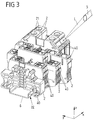
- Figure 1A and 2A show different exemplary embodiments of electrical devices 2 in the form of terminal blocks which have slots 21 for inserting electrical conductors and enable electrical conductors to be contacted and connected to one another.
- the electrical devices 2 can be attached to a mounting rail 6 in a form-fitting manner via a fastening device 22, as is exemplified in FIG Fig. 3 is shown, and can be combined on the mounting rail 6 with other electrical devices 2, for example other terminal blocks or electronic devices that, for example, take on control or automation functions in the context of an industrial plant.
- an electrical system can be created, for example, within a control cabinet.
- the mounting rail 6 can be used to arrange electrical devices 2 in a modular manner with a large number of variants for combining completely different electrical devices 2 with one another.
- inventions according to Figure 1A and 2A differ in the dimensioning of the electrical devices 2 in the form of the terminal blocks, but are otherwise functionally the same.
- the electrical devices 2 are combined with one another in the form of terminal blocks to form an assembly 1, in that identical electrical devices 2 are arranged on an auxiliary transport device in the form of a carrier tape 3.
- the electrical devices 2 are connected to one another via the carrier tape 3, so that the electrical devices 2 can be handled and, for example, transported in a simple manner. This is detailed in the DE 10 2013 112 789 A1 described, the content of which should be included here.
- the electrical devices 2 should - if they are attached to a mounting rail 6 to provide an electrical system, as in FIG Fig. 3 shown, are combined with one another - be identified via labeled marking plates 40. This is intended to make it possible to distinguish the electrical devices 2 from one another in order, for example, to identify predetermined slots 21 for electrical conductors.
- marking plates 40 are customary to label marking plates 40 and then to apply them to the electrical devices 2 already mounted on the mounting rail 6 in order to identify the electrical devices 2 in this way.
- the marking plates 40 can be individually labeled, for example on the part of the manufacturer of the electrical devices 2, and the labeled marking plates 40 can be delivered together with the electrical devices 2 (but still separately from them).
- attaching the marking plates 40 to the electrical devices 2 then requires a large amount of manual labor in order to apply individual marking plates 40 to the electrical devices 2 that have already been installed.
- the marking plates 40 be applied to the electrical devices 2 in an unlabeled manner and only after the electrical devices 2 have been mounted on the mounting rail 6 to be labeled using a laser labeling device 5.
- the electrical devices 2 are thus already provided with (but unlabeled) marking labels 40 arranged thereon provided and arranged on the support rail 6 and are then, after assembly on the support rail 6, individually inscribed by the laser inscription device 5.
- the marking plates 40 are not located in one plane.
- the use of a laser labeling device 5 which generates a flexibly controllable and alignable laser beam L for labeling enables contactless labeling of the marking plates 40 arranged in different labeling planes in a simple and reliable manner.
- electrical devices 2 As in FIG Figure 1A and 2A shown, initially combined to form an assembly 1, this assembly 1 being connected to one another in the illustrated embodiment via a carrier tape 3 and the electrical devices 2 thus being held in position with respect to one another.
- the electrical devices 2 are lined up along a longitudinal direction X in such a way that marking fields 20 of the electrical devices 2 adjoin one another along the longitudinal direction X and form a contiguous row extending along the longitudinal direction X.
- a contiguous groove N extending along the longitudinal direction X is formed on the assembly 1.
- a contiguous marking strip 4 can be used by the marking strip 4 is glued to the row of marking fields 20.
- undercuts 200 are formed on the lateral edges of the groove N, so that when the marking strip 4 is inserted into the groove N, a form fit between the marking strip 4 and the undercuts 200 is produced.
- the marking strip 4 can have a trapezoidal shape tapering in the attachment direction in cross-section transverse to the longitudinal direction X, which facilitates the insertion of the marking strip 4 into the groove N.
- the electrical devices 2 each have two opposite marking fields 20 which, when lined up to form the assembly 1, form two opposite grooves N, into each of which a marking strip 4 can be inserted.
- FIG Figures 4A, 4B and 5A, 5B shown along the longitudinal direction X are lined up marking plates 40, which are connected to one another on a first side via a fixing strip 41 and on a second side facing away from the first side carry an adhesive layer 402, via which the individual marking plates 40 on assigned marking fields 20 of the electrical devices 2 can be glued.
- the embodiments according to Figures 4A, 4B and 5A, 5B differ in the division of the marking plates 40 along the longitudinal axis X:
- the exemplary embodiment according to FIG Figures 4A, 4B has a comparatively small division with marking plates 40 which are short in the longitudinal axis X and is therefore suitable for comparatively narrow electrical devices 2.
- the embodiment according to Figures 5A, 5B on the other hand, in the longitudinal direction X, it has a comparatively large pitch with marking plates 40 which are comparatively long in the longitudinal direction X.
- the marking plates 40 are connected to one another via the fixing strips 41, so that a coherent marking strip 4 is created.
- the marking plates 40 are basically present individually and are individually connected to the fixing strip 41.
- the fixing strip 41 is detachable so that the marking plates 40 can be separated by pulling off the fixing strip 41.
- the assembly 1 of the electrical devices 2 is present with marking plates 40 which can be written on arranged on the marking fields 20, as shown in FIG Figure 1C and 2C is shown.
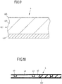
- FIG. 11 shows a cross-sectional view through the marking strip 4 along the line AA in FIG Figures 4A and 5A .
- Each marking label 40 is formed by a base layer 401 which, in the exemplary embodiment shown, is provided with a cover layer 400 on the side facing the fixing strip 41 and has an adhesive layer 402 on the side facing away from the fixing strip 41.
- the fixing strip 41 is arranged on the cover layer 400, and over the fixing strip 41 are the Marking plates 40 connected to one another.
- a protective film can be applied in order to prevent the marking plates 40 from sticking inadvertently.
- the marker plates 40 are, as in FIG Fig. 3 shown schematically, laser markable.
- a laser beam L from a laser marking device 5 can be directed onto a single marking plate 40 in order to individually mark the marking plate 40 of an electrical device 2 already arranged on a mounting rail 6.
- the cover layer 400 is removed in certain areas by means of the laser beam L.
- the cover layer 400 and the base layer 401 for example, have a different color and thus, by removing the cover layer 400, inscription with the contrast of the different colors of the cover layer 400 and the base layer 401 is produced.
- laser-inscribable materials are available, which can be single-layer or multi-layered.
- a single-layer material with only one base layer 401 can also be used.
- a laser beam L causes a material change on the base layer 401, which leads to a change in color and thereby produces an inscription.
- PC Polycarbonate
- PBT polybutylene terephthalate
- ABS acrylic butadiene styrene
- PC can be directly laser marked due to its carbon content.
- a laser beam causes a carbonization of the material and thus a changed color, which can be used for labeling.
- the materials can optionally have additional additives for improved laser writability.
- the present concept is based on the fact that initially a coherent marking strip 4 with separable marking plates 40 is arranged on an assembly 1 of electrical devices 2.
- the electrical devices 2 are preferably of the same design and thus have the same dimensions, so that a contiguous row of marking fields 20 is created by lining up the electrical devices 2, on which the marking strip 4 can be arranged.
- the assembly 1 can be used, for example, in an automatic equipping machine for equipping a mounting rail 6, so that individual electrical devices 2 can be removed and attached to a mounting rail 6. After placing it on the mounting rail 6, the marking plates 40 attached to the electrical devices 2 can then be individually labeled.
- the labeling is therefore preferably carried out when the electrical devices 2 are already attached to the mounting rail 6.
- the marking strip 4 is coherent in its initial state and has marking plates 40 lined up in a row, which can be separated in order to assign individual marking plates 40 to individual electrical devices 2.
- the use of a fixing strip 41 is not mandatory here, but the marking plates 40 can also be connected to one another in another way in the initial state of the marking strip 4, but can be separated.
- FIGS 7A, 7B and 8A, 8B show Figures 7A, 7B and 8A, 8B , these two exemplary embodiments - analogously to the exemplary embodiments according to FIG Figures 4A, 4B and 5A, 5B - Only differentiate on the basis of the division of the marking plates 40 along the longitudinal direction X.
- the exemplary embodiment according to FIG Figures 7A, 7B a comparatively small division with short marking plates 40 (measured in the longitudinal direction X).
- the embodiment according to Figures 8A, 8B In contrast, it has a comparatively large pitch with marking plates 40 which are long in the longitudinal direction X.
- the marking plates 40 are connected to one another in one piece in the initial state, so that an integral, coherent marking strip 4 is created.
- the basic structure of the individual marking plates 40 is as shown in the sectional view according to FIG Fig. 9 can be seen, identical to the structure of the marking plates 40 in the embodiment according to FIG Figures 4A, 4B and 5A, 5B , but in the initial state there is no fixing strip 41 (as in the sectional view according to FIG Fig. 6 ) is available.
- the marking plates 40 are integrally connected to one another in the initial state, as is shown in the enlarged illustration according to FIG Fig. 10 can be seen.
- the marking plates 40 are integrally connected to one another in the initial state, but are structurally subdivided by means of separating lines 42 molded into the marking strips 4 and can thus be separated.
- the individual marking plates 40 can be separated from one another along the dividing lines 42 and thus isolated, which can be done by a (cutting) tool or by tearing the marking strip 4 along the dividing lines 42 when the electrical devices 2 of the assembly 1 are isolated.
- the marking plates 40 in the initial state can be surrounded by excess material 44 which is structurally separated from the marking plates 40 by means of separating lines 43 formed in the marking strips 4.
- An adhesive layer 402 is only provided on the marking plates 40, but not on the excess material 44, so that the excess material 44 can be easily removed before or after sticking the marking strip 4 to the assembly 1 of electrical devices 2 by tearing at the dividing lines 43 .
- very different laser-inscribable materials can be used to produce the marking plates. These materials can have a single layer or a multilayer structure.
- a fixing strip for connecting the marking plates to one another in the initial state, this fixing strip can be detached from the marking plates in a simple manner without adhesive residues remaining on the marking plates.
- a weakly adhesive adhesive can be used to connect the fixing strip to the marking plates in the initial state.
- the adhesive layer for connecting the marking plates to the electrical devices is strongly adhesive and thus creates a firm connection between the individual marking plates and the associated marking fields on the electrical devices.
- the electrical devices can be made very differently.
- the electrical devices can be implemented as terminal blocks.
Claims (8)
- Procédé de placement de plaquettes de marquage (40) sur plusieurs appareils électriques (2) qui peuvent être disposés sur un rail de support (6), chacun des appareils électriques présentant un champ de marquage (20) sur lequel peut être fixée une plaquette de marquage (40) pouvant recevoir une inscription, et dans lequel lors du procédé- les appareils électriques (2) peuvent être disposés les uns contre les autres en rangées dans une direction longitudinale (X) pour ainsi former un module de montage (1), de telle sorte que les champs de marquage (20) des appareils électriques (2) se raccordent les uns aux autres dans la direction longitudinale (X) et forment une rangée continue qui s'étend dans la direction longitudinale (X),caractérisé par les étapes qui consistent à :- fixer sur la rangée d'appareils électriques (2) un ruban continu de marquage (4) qui présente plusieurs des plaquettes de marquage (40) pouvant recevoir une inscription à l'aide d'un dispositif (5) d'inscription par laser et associées aux champs de marquage (20) des appareils électriques (2) et- après avoir placé le ruban de marquage (4), séparer une à une les plaquettes de marquage (40) de telle sorte qu'au moins une plaquette de marquage (40) soit disposée sur le champ de marquage (20) de chaque appareil électrique (2) .
- Procédé selon la revendication 1, caractérisé en ce que le ruban continu de marquage (4) est collé sur les appareils électriques (2) le long de la rangée de champs de marquage (20).
- Procédé selon les revendications 1 ou 2, caractérisé en ce que les champs de marquage (20) sont formés dans des creux des appareils électriques (2) et en ce que par le placement des appareils électriques (2) les uns contre les autres est formée une rainure (N) continue s'étendant dans la direction longitudinale (X) et dans laquelle est fixé le ruban de marquage (4).
- Procédé selon la revendication 3, caractérisé en ce que le ruban de marquage (4) est fixé dans la rainure (N) en correspondance géométrique.
- Procédé selon l'une quelconque des revendications précédentes, caractérisé en ce que pour former le module de montage (1), les appareils électriques (2) sont rangés les uns contre les autres sur une bande de support (3) qui s'étend dans la direction longitudinale (X).
- Procédé selon l'une quelconque des revendications 1 à 5, caractérisé en ce que les plaquettes de marquage (40) sont initialement reliées les unes aux autres par l'intermédiaire d'un ruban de fixation (41) et sont ensuite séparées une à une par enlèvement du ruban de fixation (41).
- Procédé selon l'une quelconque des revendications 1 à 5, caractérisé en ce que les plaquettes de marquage (40) sont initialement reliées les unes aux autres d'un seul tenant et sont séparées les unes des autres en séparant les plaquettes de marquage (40) les unes des autres le long de lignes de séparation (42) formées sur le ruban de marquage (4).
- Procédé pour équiper un rail de support (6) d'appareils électriques (2) sur lesquels des plaquettes de marquage (40) sont fixées en recourant à un procédé selon l'une quelconque des revendications précédentes, caractérisé par les étapes qui consistent à :- enlever un appareil électrique (2) du module de montage formé par les appareils électriques (2) rangés les uns contre les autres,- placer l'appareil électrique (2) sur le rail de support (6) et- à l'aide d'un dispositif (5) d'inscription par laser, apporter une inscription sur la ou les plaquettes de marquage (40) de l'appareil électrique (2) qui a été enlevé et placé sur le rail de support (6).
Priority Applications (1)
| Application Number | Priority Date | Filing Date | Title |
|---|---|---|---|
| PL17705017T PL3405941T3 (pl) | 2016-01-18 | 2017-01-17 | Sposób mocowania tabliczek znakujących na wielu urządzeniach elektrycznych, które mogą być umieszczone na szynie nośnej |
Applications Claiming Priority (3)
| Application Number | Priority Date | Filing Date | Title |
|---|---|---|---|
| DE102016100722.6A DE102016100722B4 (de) | 2016-01-18 | 2016-01-18 | Verfahren zum Bestücken einer Tragschiene mit elektrischen Geräten |
| DE102016107459.4A DE102016107459A1 (de) | 2016-04-22 | 2016-04-22 | Verfahren zur Markierung von elektrischen Bauelementen |
| PCT/EP2017/050879 WO2017125385A1 (fr) | 2016-01-18 | 2017-01-17 | Procédé de pose d'étiquettes de repérage sur une pluralité d'appareils électriques pouvant être rangés sur un rail porteur |
Publications (2)
| Publication Number | Publication Date |
|---|---|
| EP3405941A1 EP3405941A1 (fr) | 2018-11-28 |
| EP3405941B1 true EP3405941B1 (fr) | 2021-04-28 |
Family
ID=57821982
Family Applications (2)
| Application Number | Title | Priority Date | Filing Date |
|---|---|---|---|
| EP17700534.5A Active EP3405351B1 (fr) | 2016-01-18 | 2017-01-17 | Dispositif de marquage pour composants électriques |
| EP17705017.6A Active EP3405941B1 (fr) | 2016-01-18 | 2017-01-17 | Procédé de pose d'étiquettes de repérage sur une pluralité d'appareils électriques pouvant être rangés sur un rail porteur |
Family Applications Before (1)
| Application Number | Title | Priority Date | Filing Date |
|---|---|---|---|
| EP17700534.5A Active EP3405351B1 (fr) | 2016-01-18 | 2017-01-17 | Dispositif de marquage pour composants électriques |
Country Status (11)
| Country | Link |
|---|---|
| US (2) | US10586474B2 (fr) |
| EP (2) | EP3405351B1 (fr) |
| JP (1) | JP6723367B2 (fr) |
| KR (1) | KR102152513B1 (fr) |
| CN (2) | CN108698422B (fr) |
| BR (2) | BR112018014160B1 (fr) |
| ES (2) | ES2875512T3 (fr) |
| MX (1) | MX2018008777A (fr) |
| PL (2) | PL3405941T3 (fr) |
| RU (2) | RU2698019C1 (fr) |
| WO (2) | WO2017125385A1 (fr) |
Families Citing this family (6)
| Publication number | Priority date | Publication date | Assignee | Title |
|---|---|---|---|---|
| PL3405941T3 (pl) * | 2016-01-18 | 2021-09-27 | Phoenix Contact Gmbh & Co. Kg | Sposób mocowania tabliczek znakujących na wielu urządzeniach elektrycznych, które mogą być umieszczone na szynie nośnej |
| WO2020200639A1 (fr) | 2019-03-29 | 2020-10-08 | Weidmüller Interface GmbH & Co. KG | Procédé et dispositif de marquage de dispositifs électriques pouvant être disposés en ligne |
| DE102019108297A1 (de) * | 2019-03-29 | 2020-10-01 | Weidmüller Interface GmbH & Co. KG | Vorrichtung zum Markieren von aneinanderreihbaren elektrischen Geräten |
| DE102019108298A1 (de) * | 2019-03-29 | 2020-10-01 | Weidmüller Interface GmbH & Co. KG | Verfahren und Vorrichtung zum Markieren von aneinanderreihbaren elektrischen Geräten |
| BE1027784B1 (de) * | 2019-11-25 | 2021-06-23 | Phoenix Contact Gmbh & Co | Verfahren zum Herstellen einer elektrischen Anschlussanordnung und elektrische Anschlussanordnung |
| US11932036B2 (en) | 2019-11-25 | 2024-03-19 | Weidmüller Interface GmbH & Co. KG | Method and device for marking electrical devices which can be arranged in a row |
Family Cites Families (45)
| Publication number | Priority date | Publication date | Assignee | Title |
|---|---|---|---|---|
| DE1857546U (de) | 1962-06-29 | 1962-08-30 | Josef Eisert | Vorrichtung zur kennzeichnung von schaltanlagen-reihenklemmen. |
| DE1956966U (de) | 1966-10-26 | 1967-03-16 | C A Weidmueller K G | Vorrichtung zur einheitlichen kennzeichnung von geraeten und bauteilen, insbesondere von elektrischen reihenklemmen. |
| US3496521A (en) * | 1967-05-29 | 1970-02-17 | Wago Kontakttechnik Gmbh | Safety contact terminal for electric wires |
| DE1622223B2 (de) | 1968-02-02 | 1972-03-30 | Ernst Leitz Gmbh, 6330 Wetzlar | Einschaltvorrichtung fuer den blendenregler in kinematografischen kameras |
| FR1593558A (fr) | 1968-07-25 | 1970-06-01 | ||
| US3824553A (en) * | 1973-06-22 | 1974-07-16 | Amp Inc | Low voltage terminal strip capable of withstanding high voltage transients |
| JPS5352442A (en) | 1976-10-23 | 1978-05-12 | Fujitsu Ltd | Laser recorder |
| DD134838B1 (de) | 1978-03-01 | 1980-08-06 | Heinz Kiepsch | Verfahren zum fixieren von schablonen |
| DE3333386A1 (de) | 1983-09-15 | 1985-04-11 | Siemens AG, 1000 Berlin und 8000 München | Verfahren und einrichtung zum beschriften von teilen, insbesondere von elektronischen bauelementen |
| JPH09220686A (ja) | 1996-02-13 | 1997-08-26 | Tdk Corp | レーザ印字方法及び装置 |
| US5855969A (en) | 1996-06-10 | 1999-01-05 | Infosight Corp. | CO2 laser marking of coated surfaces for product identification |
| US5993267A (en) | 1998-03-16 | 1999-11-30 | Lin; Y. S. | Terminal block |
| DE10009750B4 (de) | 2000-03-01 | 2004-10-14 | Amphenol-Tuchel Electronics Gmbh | Schutzleiterverbindung |
| DE10119456C1 (de) * | 2001-04-20 | 2003-05-08 | Siemens Ag | Beschriftungsverfahren für ein elektrisches Gerät |
| ATE325715T1 (de) * | 2001-10-09 | 2006-06-15 | Koninkl Philips Electronics Nv | Verfahren zur herstellung eines elektronischen bauelements und elektronisches bauelement davon hergestellt |
| DE10213110A1 (de) | 2002-03-23 | 2003-10-02 | Tesa Ag | Mehrschichtige Laser-Transferfolie zum dauerhaften Beschriften von Bauteilen |
| DE20303475U1 (de) | 2003-03-05 | 2003-05-15 | Wago Verwaltungs Gmbh | Multifunktionale Beschriftungsaufnahme |
| DE10325179A1 (de) * | 2003-06-04 | 2004-12-23 | Marconi Communications Gmbh | Verfahren zum Montieren einer Schaltung |
| JP4254514B2 (ja) | 2003-12-15 | 2009-04-15 | 株式会社村田製作所 | 電子部品のマーキング形成方法及び電子部品 |
| DE202004011704U1 (de) | 2004-07-26 | 2004-09-30 | Fahrzeugelektrik Pirna Gmbh | Elektrische Verbindungsvorrichtung für Kraftfahrzeuge |
| DE102005053565A1 (de) | 2005-11-08 | 2007-07-12 | Aloys Mennekes Anlagengesellschaft Mbh & Co. Kg | Steckerstift mit Schneidklemme |
| DE102006019118B4 (de) | 2006-04-25 | 2011-08-18 | Epcos Ag, 81669 | Bauelement mit optischer Markierung und Verfahren zur Herstellung |
| DE102007011179A1 (de) * | 2007-03-06 | 2008-09-11 | Murrplastik Systemtechnik Gmbh | Vorrichtung zur Beschriftung von Kennzeichnungsschildern |
| JP2008303475A (ja) * | 2007-06-05 | 2008-12-18 | Horihokku:Kk | 靴下 |
| CN101221839B (zh) * | 2007-12-19 | 2010-07-14 | 李世武 | 一种端子标记/线号/电缆标牌的实现方法及装置 |
| DE102008032837A1 (de) | 2008-07-14 | 2010-01-21 | Phoenix Contact Gmbh & Co. Kg | Elektrische Anschlussvorrichtung |
| DE202008010347U1 (de) | 2008-08-04 | 2008-10-02 | Wago Verwaltungsgesellschaft Mbh | Steckbarer PE-Schutzkontakt |
| DE102009017999A1 (de) | 2008-11-18 | 2010-05-20 | Weidmüller Interface GmbH & Co. KG | Verfahren zur automatisierten Montage von anreihbaren Geräten auf einer Montagebasis und Montageanordnung |
| DE102009006793A1 (de) | 2009-01-30 | 2010-08-05 | Phoenix Contact Gmbh & Co. Kg | Multifunktionsvorrichtung zur Konfektionierung von Markierungsschildern |
| CH700111B1 (fr) * | 2009-09-25 | 2010-06-30 | Agie Sa | Machine d'usinage par laser. |
| DE102009056713A1 (de) | 2009-12-04 | 2011-06-09 | Phoenix Contact Gmbh & Co. Kg | Steckverbinder-Einrichtung |
| ITMI20100017U1 (it) * | 2010-01-28 | 2011-07-29 | Morsettitalia Spa | Morsetto di collegamento elettrico da quadro con alloggiamento porta etichetta, etichetta per detto alloggiamento e relativo assieme morsetto/etichetta |
| DE202010005767U1 (de) * | 2010-04-16 | 2011-09-23 | Weidmüller Interface GmbH & Co. KG | Transporteinheit |
| DE102010022690B4 (de) | 2010-06-04 | 2012-04-12 | Harting Electric Gmbh & Co. Kg | Elektrischer Steckverbinder mit PE-Kontakt |
| DE102010034993A1 (de) | 2010-08-20 | 2012-02-23 | Phoenix Contact Gmbh & Co. Kg | Kennzeichnungsmatte zur Kennzeichnung elektrischer Bauelemente und Verfahren zur Herstellung einer solchen Kennzeichnungsmatte |
| DE102010047369A1 (de) | 2010-10-05 | 2012-04-05 | Phoenix Contact Gmbh & Co. Kg | Verfahren zur Montage von Bauteilen auf einer Tragschiene sowie System zur Durchführung des Verfahrens |
| US8857860B2 (en) * | 2011-03-29 | 2014-10-14 | Composite Lining Systems, LP | Coupling assembly with corrosion barrier for GRE-lined premium threaded pipe |
| CN202192857U (zh) * | 2011-08-31 | 2012-04-18 | 重庆旭安科技有限责任公司 | 线缆激光打标机 |
| EP2792499A1 (fr) * | 2013-04-19 | 2014-10-22 | Siemens Aktiengesellschaft | Procédé destiné à l'inscription sur un composant |
| DE102013012389B4 (de) | 2013-07-26 | 2015-10-01 | Phoenix Contact Gmbh & Co. Kg | Vorrichtung und Verfahren zur Montage eines Kennzeichnungsschildes |
| DE102013112789B4 (de) | 2013-11-19 | 2017-09-28 | Phoenix Contact Gmbh & Co. Kg | Transporthilfsvorrichtung sowie Anordnung mit einem aus elektromechanischen Bauelementen gebildeten Strang und einer entsprechenden Transporthilfsvorrichtung |
| DE102013113328A1 (de) | 2013-12-02 | 2015-06-03 | Phoenix Contact Gmbh & Co. Kg | Schildstreifen mit mehreren bedruckbaren Kennzeichnungsschildern und Magazin zum Einführen von Schildstreifen in eine Druckvorrichtung |
| DE102015109020A1 (de) | 2014-09-10 | 2016-03-10 | Weidmüller Interface GmbH & Co. KG | Markiererstreifen |
| US10062979B2 (en) * | 2015-08-21 | 2018-08-28 | Panduit Corp. | Terminal block marker |
| PL3405941T3 (pl) * | 2016-01-18 | 2021-09-27 | Phoenix Contact Gmbh & Co. Kg | Sposób mocowania tabliczek znakujących na wielu urządzeniach elektrycznych, które mogą być umieszczone na szynie nośnej |
-
2017
- 2017-01-17 PL PL17705017T patent/PL3405941T3/pl unknown
- 2017-01-17 KR KR1020187022132A patent/KR102152513B1/ko active IP Right Grant
- 2017-01-17 CN CN201780007118.9A patent/CN108698422B/zh active Active
- 2017-01-17 RU RU2018126479A patent/RU2698019C1/ru active
- 2017-01-17 CN CN201780007131.4A patent/CN108604426B/zh active Active
- 2017-01-17 WO PCT/EP2017/050879 patent/WO2017125385A1/fr active Application Filing
- 2017-01-17 ES ES17705017T patent/ES2875512T3/es active Active
- 2017-01-17 EP EP17700534.5A patent/EP3405351B1/fr active Active
- 2017-01-17 US US16/070,525 patent/US10586474B2/en active Active
- 2017-01-17 MX MX2018008777A patent/MX2018008777A/es active IP Right Grant
- 2017-01-17 PL PL17700534.5T patent/PL3405351T3/pl unknown
- 2017-01-17 RU RU2018129977A patent/RU2695838C1/ru active
- 2017-01-17 JP JP2018537478A patent/JP6723367B2/ja active Active
- 2017-01-17 WO PCT/EP2017/050838 patent/WO2017125364A1/fr active Application Filing
- 2017-01-17 ES ES17700534T patent/ES2950334T3/es active Active
- 2017-01-17 EP EP17705017.6A patent/EP3405941B1/fr active Active
- 2017-01-17 BR BR112018014160-7A patent/BR112018014160B1/pt active IP Right Grant
- 2017-01-17 US US16/067,632 patent/US10657848B2/en active Active
- 2017-01-17 BR BR112018014462-2A patent/BR112018014462A2/pt not_active Application Discontinuation
Non-Patent Citations (1)
| Title |
|---|
| None * |
Also Published As
| Publication number | Publication date |
|---|---|
| KR20180100179A (ko) | 2018-09-07 |
| EP3405351A1 (fr) | 2018-11-28 |
| CN108698422A (zh) | 2018-10-23 |
| EP3405941A1 (fr) | 2018-11-28 |
| CN108698422B (zh) | 2020-08-14 |
| EP3405351B1 (fr) | 2023-06-28 |
| US20190027070A1 (en) | 2019-01-24 |
| CN108604426A (zh) | 2018-09-28 |
| BR112018014462A2 (pt) | 2018-12-11 |
| US20190009573A1 (en) | 2019-01-10 |
| PL3405351T3 (pl) | 2023-09-18 |
| MX2018008777A (es) | 2018-09-28 |
| RU2695838C1 (ru) | 2019-07-29 |
| CN108604426B (zh) | 2021-02-05 |
| BR112018014160A2 (pt) | 2018-12-11 |
| ES2950334T3 (es) | 2023-10-09 |
| RU2698019C1 (ru) | 2019-08-21 |
| JP6723367B2 (ja) | 2020-07-15 |
| PL3405941T3 (pl) | 2021-09-27 |
| WO2017125364A1 (fr) | 2017-07-27 |
| KR102152513B1 (ko) | 2020-10-26 |
| WO2017125385A1 (fr) | 2017-07-27 |
| US10657848B2 (en) | 2020-05-19 |
| US10586474B2 (en) | 2020-03-10 |
| ES2875512T3 (es) | 2021-11-10 |
| JP2019503274A (ja) | 2019-02-07 |
| BR112018014160B1 (pt) | 2022-09-27 |
Similar Documents
| Publication | Publication Date | Title |
|---|---|---|
| EP3405941B1 (fr) | Procédé de pose d'étiquettes de repérage sur une pluralité d'appareils électriques pouvant être rangés sur un rail porteur | |
| DE102016100722B4 (de) | Verfahren zum Bestücken einer Tragschiene mit elektrischen Geräten | |
| EP3078018B1 (fr) | Bande de plaques comportant plusieurs plaques d'identification imprimables et magasin destiné à l'insertion de bandes de plaques dans un dispositif d'impression | |
| EP2391999B1 (fr) | Dispositif multifonctionnel destiné à la confection d'étiquettes de marquage | |
| DE102009017999A1 (de) | Verfahren zur automatisierten Montage von anreihbaren Geräten auf einer Montagebasis und Montageanordnung | |
| DE2829620C2 (de) | Bezeichnungsschilderstreifen für die Kennzeichnung insbesondere von Reihenklemmen | |
| DE102010053081A1 (de) | Verfahren zur Verarbeitung plattenförmiger Erzeugnisse | |
| AT12320U1 (de) | Verfahren zum verbinden einer mehrzahl von elementen einer leiterplatte, leiterplatte sowie verwendung eines derartigen verfahrens | |
| DE102014004353A1 (de) | Vorrichtung zur Beschriftung von Kennzeichnungseinheiten | |
| EP1958178A1 (fr) | Jeu de plaquettes d'identification | |
| EP2407014B1 (fr) | Procédé et système de connexion d'une pluralité de cartes de circuit imprimé à au moins un élément support ou cadre | |
| DE102012007004B3 (de) | Kennzeichnungseinrichtung für Schaltschränke und andere elektrische Einrichtungen | |
| EP2235714B1 (fr) | Support de gaine rétractable et procédé d'insertion de câbles dans des gaines rétractables | |
| WO2007147470A1 (fr) | Procédé de production d'une pièce moulée par injection comprenant une carte imprimée souple intégrée | |
| DE2809789A1 (de) | Verfahren und vorrichtung zum montieren eines elektrischen bauelementes auf einer leiterplatte | |
| DE102015102958B4 (de) | Verfahren zur Beschriftung einer Reihenklemme | |
| EP2338320A1 (fr) | Recouvrement protecteur pour plaquette à circuit imprimé souple | |
| AT12722U1 (de) | Verfahren und verbund zum bearbeiten bzw. behandeln einer mehrzahl von leiterplatten sowie verwendung hiefür | |
| DE4226069A1 (de) | Adaptereinrichtung für eine automatische Prüfvorrichtung zum Prüfen von Schaltungsplatinen | |
| DE602004009010T2 (de) | Träger für Kabelkennzeichnungshülsen angepasst an Drückträgern. | |
| DE102016107459A1 (de) | Verfahren zur Markierung von elektrischen Bauelementen | |
| EP4181639A1 (fr) | Dispositifs et procédés de montage d'un module à affichages multiples | |
| EP2908305B1 (fr) | Système de sections de tuyaux | |
| DE10244498A1 (de) | Transportträger zur lagegenauen Teilezuführung | |
| DE102014114103B4 (de) | Kennzeichnungsstreifen und Verfahren zu dessen Kennzeichnung |
Legal Events
| Date | Code | Title | Description |
|---|---|---|---|
| STAA | Information on the status of an ep patent application or granted ep patent |
Free format text: STATUS: UNKNOWN |
|
| STAA | Information on the status of an ep patent application or granted ep patent |
Free format text: STATUS: THE INTERNATIONAL PUBLICATION HAS BEEN MADE |
|
| PUAI | Public reference made under article 153(3) epc to a published international application that has entered the european phase |
Free format text: ORIGINAL CODE: 0009012 |
|
| STAA | Information on the status of an ep patent application or granted ep patent |
Free format text: STATUS: REQUEST FOR EXAMINATION WAS MADE |
|
| 17P | Request for examination filed |
Effective date: 20180730 |
|
| AK | Designated contracting states |
Kind code of ref document: A1 Designated state(s): AL AT BE BG CH CY CZ DE DK EE ES FI FR GB GR HR HU IE IS IT LI LT LU LV MC MK MT NL NO PL PT RO RS SE SI SK SM TR |
|
| AX | Request for extension of the european patent |
Extension state: BA ME |
|
| DAV | Request for validation of the european patent (deleted) | ||
| DAX | Request for extension of the european patent (deleted) | ||
| GRAP | Despatch of communication of intention to grant a patent |
Free format text: ORIGINAL CODE: EPIDOSNIGR1 |
|
| STAA | Information on the status of an ep patent application or granted ep patent |
Free format text: STATUS: GRANT OF PATENT IS INTENDED |
|
| INTG | Intention to grant announced |
Effective date: 20201125 |
|
| GRAS | Grant fee paid |
Free format text: ORIGINAL CODE: EPIDOSNIGR3 |
|
| GRAA | (expected) grant |
Free format text: ORIGINAL CODE: 0009210 |
|
| STAA | Information on the status of an ep patent application or granted ep patent |
Free format text: STATUS: THE PATENT HAS BEEN GRANTED |
|
| AK | Designated contracting states |
Kind code of ref document: B1 Designated state(s): AL AT BE BG CH CY CZ DE DK EE ES FI FR GB GR HR HU IE IS IT LI LT LU LV MC MK MT NL NO PL PT RO RS SE SI SK SM TR |
|
| REG | Reference to a national code |
Ref country code: GB Ref legal event code: FG4D Free format text: NOT ENGLISH |
|
| REG | Reference to a national code |
Ref country code: CH Ref legal event code: EP |
|
| REG | Reference to a national code |
Ref country code: AT Ref legal event code: REF Ref document number: 1387982 Country of ref document: AT Kind code of ref document: T Effective date: 20210515 |
|
| REG | Reference to a national code |
Ref country code: DE Ref legal event code: R096 Ref document number: 502017010191 Country of ref document: DE |
|
| REG | Reference to a national code |
Ref country code: IE Ref legal event code: FG4D Free format text: LANGUAGE OF EP DOCUMENT: GERMAN |
|
| REG | Reference to a national code |
Ref country code: FI Ref legal event code: FGE |
|
| REG | Reference to a national code |
Ref country code: NL Ref legal event code: FP |
|
| REG | Reference to a national code |
Ref country code: LT Ref legal event code: MG9D |
|
| PG25 | Lapsed in a contracting state [announced via postgrant information from national office to epo] |
Ref country code: HR Free format text: LAPSE BECAUSE OF FAILURE TO SUBMIT A TRANSLATION OF THE DESCRIPTION OR TO PAY THE FEE WITHIN THE PRESCRIBED TIME-LIMIT Effective date: 20210428 Ref country code: BG Free format text: LAPSE BECAUSE OF FAILURE TO SUBMIT A TRANSLATION OF THE DESCRIPTION OR TO PAY THE FEE WITHIN THE PRESCRIBED TIME-LIMIT Effective date: 20210728 Ref country code: LT Free format text: LAPSE BECAUSE OF FAILURE TO SUBMIT A TRANSLATION OF THE DESCRIPTION OR TO PAY THE FEE WITHIN THE PRESCRIBED TIME-LIMIT Effective date: 20210428 |
|
| REG | Reference to a national code |
Ref country code: ES Ref legal event code: FG2A Ref document number: 2875512 Country of ref document: ES Kind code of ref document: T3 Effective date: 20211110 |
|
| PG25 | Lapsed in a contracting state [announced via postgrant information from national office to epo] |
Ref country code: SE Free format text: LAPSE BECAUSE OF FAILURE TO SUBMIT A TRANSLATION OF THE DESCRIPTION OR TO PAY THE FEE WITHIN THE PRESCRIBED TIME-LIMIT Effective date: 20210428 Ref country code: RS Free format text: LAPSE BECAUSE OF FAILURE TO SUBMIT A TRANSLATION OF THE DESCRIPTION OR TO PAY THE FEE WITHIN THE PRESCRIBED TIME-LIMIT Effective date: 20210428 Ref country code: PT Free format text: LAPSE BECAUSE OF FAILURE TO SUBMIT A TRANSLATION OF THE DESCRIPTION OR TO PAY THE FEE WITHIN THE PRESCRIBED TIME-LIMIT Effective date: 20210830 Ref country code: NO Free format text: LAPSE BECAUSE OF FAILURE TO SUBMIT A TRANSLATION OF THE DESCRIPTION OR TO PAY THE FEE WITHIN THE PRESCRIBED TIME-LIMIT Effective date: 20210728 Ref country code: GR Free format text: LAPSE BECAUSE OF FAILURE TO SUBMIT A TRANSLATION OF THE DESCRIPTION OR TO PAY THE FEE WITHIN THE PRESCRIBED TIME-LIMIT Effective date: 20210729 Ref country code: IS Free format text: LAPSE BECAUSE OF FAILURE TO SUBMIT A TRANSLATION OF THE DESCRIPTION OR TO PAY THE FEE WITHIN THE PRESCRIBED TIME-LIMIT Effective date: 20210828 Ref country code: LV Free format text: LAPSE BECAUSE OF FAILURE TO SUBMIT A TRANSLATION OF THE DESCRIPTION OR TO PAY THE FEE WITHIN THE PRESCRIBED TIME-LIMIT Effective date: 20210428 |
|
| PG25 | Lapsed in a contracting state [announced via postgrant information from national office to epo] |
Ref country code: SM Free format text: LAPSE BECAUSE OF FAILURE TO SUBMIT A TRANSLATION OF THE DESCRIPTION OR TO PAY THE FEE WITHIN THE PRESCRIBED TIME-LIMIT Effective date: 20210428 Ref country code: SK Free format text: LAPSE BECAUSE OF FAILURE TO SUBMIT A TRANSLATION OF THE DESCRIPTION OR TO PAY THE FEE WITHIN THE PRESCRIBED TIME-LIMIT Effective date: 20210428 Ref country code: RO Free format text: LAPSE BECAUSE OF FAILURE TO SUBMIT A TRANSLATION OF THE DESCRIPTION OR TO PAY THE FEE WITHIN THE PRESCRIBED TIME-LIMIT Effective date: 20210428 Ref country code: DK Free format text: LAPSE BECAUSE OF FAILURE TO SUBMIT A TRANSLATION OF THE DESCRIPTION OR TO PAY THE FEE WITHIN THE PRESCRIBED TIME-LIMIT Effective date: 20210428 Ref country code: EE Free format text: LAPSE BECAUSE OF FAILURE TO SUBMIT A TRANSLATION OF THE DESCRIPTION OR TO PAY THE FEE WITHIN THE PRESCRIBED TIME-LIMIT Effective date: 20210428 Ref country code: CZ Free format text: LAPSE BECAUSE OF FAILURE TO SUBMIT A TRANSLATION OF THE DESCRIPTION OR TO PAY THE FEE WITHIN THE PRESCRIBED TIME-LIMIT Effective date: 20210428 |
|
| REG | Reference to a national code |
Ref country code: DE Ref legal event code: R097 Ref document number: 502017010191 Country of ref document: DE |
|
| PLBE | No opposition filed within time limit |
Free format text: ORIGINAL CODE: 0009261 |
|
| STAA | Information on the status of an ep patent application or granted ep patent |
Free format text: STATUS: NO OPPOSITION FILED WITHIN TIME LIMIT |
|
| 26N | No opposition filed |
Effective date: 20220131 |
|
| PG25 | Lapsed in a contracting state [announced via postgrant information from national office to epo] |
Ref country code: IS Free format text: LAPSE BECAUSE OF FAILURE TO SUBMIT A TRANSLATION OF THE DESCRIPTION OR TO PAY THE FEE WITHIN THE PRESCRIBED TIME-LIMIT Effective date: 20210828 Ref country code: AL Free format text: LAPSE BECAUSE OF FAILURE TO SUBMIT A TRANSLATION OF THE DESCRIPTION OR TO PAY THE FEE WITHIN THE PRESCRIBED TIME-LIMIT Effective date: 20210428 |
|
| PG25 | Lapsed in a contracting state [announced via postgrant information from national office to epo] |
Ref country code: MC Free format text: LAPSE BECAUSE OF FAILURE TO SUBMIT A TRANSLATION OF THE DESCRIPTION OR TO PAY THE FEE WITHIN THE PRESCRIBED TIME-LIMIT Effective date: 20210428 |
|
| GBPC | Gb: european patent ceased through non-payment of renewal fee |
Effective date: 20220117 |
|
| PG25 | Lapsed in a contracting state [announced via postgrant information from national office to epo] |
Ref country code: LU Free format text: LAPSE BECAUSE OF NON-PAYMENT OF DUE FEES Effective date: 20220117 Ref country code: GB Free format text: LAPSE BECAUSE OF NON-PAYMENT OF DUE FEES Effective date: 20220117 |
|
| PG25 | Lapsed in a contracting state [announced via postgrant information from national office to epo] |
Ref country code: IE Free format text: LAPSE BECAUSE OF NON-PAYMENT OF DUE FEES Effective date: 20220117 |
|
| PGFP | Annual fee paid to national office [announced via postgrant information from national office to epo] |
Ref country code: FR Payment date: 20230124 Year of fee payment: 7 Ref country code: FI Payment date: 20230118 Year of fee payment: 7 Ref country code: ES Payment date: 20230228 Year of fee payment: 7 Ref country code: CH Payment date: 20230125 Year of fee payment: 7 Ref country code: AT Payment date: 20230118 Year of fee payment: 7 |
|
| PGFP | Annual fee paid to national office [announced via postgrant information from national office to epo] |
Ref country code: PL Payment date: 20230109 Year of fee payment: 7 Ref country code: IT Payment date: 20230120 Year of fee payment: 7 Ref country code: BE Payment date: 20230124 Year of fee payment: 7 |
|
| P01 | Opt-out of the competence of the unified patent court (upc) registered |
Effective date: 20230424 |
|
| PGFP | Annual fee paid to national office [announced via postgrant information from national office to epo] |
Ref country code: NL Payment date: 20240125 Year of fee payment: 8 |
|
| PG25 | Lapsed in a contracting state [announced via postgrant information from national office to epo] |
Ref country code: HU Free format text: LAPSE BECAUSE OF FAILURE TO SUBMIT A TRANSLATION OF THE DESCRIPTION OR TO PAY THE FEE WITHIN THE PRESCRIBED TIME-LIMIT; INVALID AB INITIO Effective date: 20170117 |
|
| PGFP | Annual fee paid to national office [announced via postgrant information from national office to epo] |
Ref country code: ES Payment date: 20240209 Year of fee payment: 8 |
|
| PGFP | Annual fee paid to national office [announced via postgrant information from national office to epo] |
Ref country code: AT Payment date: 20240118 Year of fee payment: 8 |
|
| PG25 | Lapsed in a contracting state [announced via postgrant information from national office to epo] |
Ref country code: MK Free format text: LAPSE BECAUSE OF FAILURE TO SUBMIT A TRANSLATION OF THE DESCRIPTION OR TO PAY THE FEE WITHIN THE PRESCRIBED TIME-LIMIT Effective date: 20210428 Ref country code: CY Free format text: LAPSE BECAUSE OF FAILURE TO SUBMIT A TRANSLATION OF THE DESCRIPTION OR TO PAY THE FEE WITHIN THE PRESCRIBED TIME-LIMIT Effective date: 20210428 |
|
| PGFP | Annual fee paid to national office [announced via postgrant information from national office to epo] |
Ref country code: FI Payment date: 20240125 Year of fee payment: 8 Ref country code: DE Payment date: 20240328 Year of fee payment: 8 Ref country code: CH Payment date: 20240202 Year of fee payment: 8 |