EP3402146A1 - Phasenkompensationsvorrichtung, phasenkompensationsverfahren und kommunikationsvorrichtung - Google Patents
Phasenkompensationsvorrichtung, phasenkompensationsverfahren und kommunikationsvorrichtung Download PDFInfo
- Publication number
- EP3402146A1 EP3402146A1 EP17813006.8A EP17813006A EP3402146A1 EP 3402146 A1 EP3402146 A1 EP 3402146A1 EP 17813006 A EP17813006 A EP 17813006A EP 3402146 A1 EP3402146 A1 EP 3402146A1
- Authority
- EP
- European Patent Office
- Prior art keywords
- phase
- phase difference
- signal
- output signal
- phase compensation
- Prior art date
- Legal status (The legal status is an assumption and is not a legal conclusion. Google has not performed a legal analysis and makes no representation as to the accuracy of the status listed.)
- Granted
Links
Images


Classifications
-
- H—ELECTRICITY
- H04—ELECTRIC COMMUNICATION TECHNIQUE
- H04L—TRANSMISSION OF DIGITAL INFORMATION, e.g. TELEGRAPHIC COMMUNICATION
- H04L27/00—Modulated-carrier systems
- H04L27/32—Carrier systems characterised by combinations of two or more of the types covered by groups H04L27/02, H04L27/10, H04L27/18 or H04L27/26
- H04L27/34—Amplitude- and phase-modulated carrier systems, e.g. quadrature-amplitude modulated carrier systems
- H04L27/38—Demodulator circuits; Receiver circuits
- H04L27/3818—Demodulator circuits; Receiver circuits using coherent demodulation, i.e. using one or more nominally phase synchronous carriers
- H04L27/3836—Demodulator circuits; Receiver circuits using coherent demodulation, i.e. using one or more nominally phase synchronous carriers in which the carrier is recovered using the received modulated signal or the received IF signal, e.g. by detecting a pilot or by frequency multiplication
-
- H—ELECTRICITY
- H04—ELECTRIC COMMUNICATION TECHNIQUE
- H04B—TRANSMISSION
- H04B10/00—Transmission systems employing electromagnetic waves other than radio-waves, e.g. infrared, visible or ultraviolet light, or employing corpuscular radiation, e.g. quantum communication
- H04B10/60—Receivers
- H04B10/61—Coherent receivers
- H04B10/616—Details of the electronic signal processing in coherent optical receivers
- H04B10/6164—Estimation or correction of the frequency offset between the received optical signal and the optical local oscillator
-
- H—ELECTRICITY
- H04—ELECTRIC COMMUNICATION TECHNIQUE
- H04B—TRANSMISSION
- H04B10/00—Transmission systems employing electromagnetic waves other than radio-waves, e.g. infrared, visible or ultraviolet light, or employing corpuscular radiation, e.g. quantum communication
- H04B10/60—Receivers
- H04B10/61—Coherent receivers
- H04B10/615—Arrangements affecting the optical part of the receiver
-
- H—ELECTRICITY
- H04—ELECTRIC COMMUNICATION TECHNIQUE
- H04B—TRANSMISSION
- H04B10/00—Transmission systems employing electromagnetic waves other than radio-waves, e.g. infrared, visible or ultraviolet light, or employing corpuscular radiation, e.g. quantum communication
- H04B10/60—Receivers
- H04B10/61—Coherent receivers
- H04B10/616—Details of the electronic signal processing in coherent optical receivers
- H04B10/6165—Estimation of the phase of the received optical signal, phase error estimation or phase error correction
-
- H—ELECTRICITY
- H04—ELECTRIC COMMUNICATION TECHNIQUE
- H04L—TRANSMISSION OF DIGITAL INFORMATION, e.g. TELEGRAPHIC COMMUNICATION
- H04L27/00—Modulated-carrier systems
- H04L27/01—Equalisers
-
- H—ELECTRICITY
- H04—ELECTRIC COMMUNICATION TECHNIQUE
- H04L—TRANSMISSION OF DIGITAL INFORMATION, e.g. TELEGRAPHIC COMMUNICATION
- H04L27/00—Modulated-carrier systems
- H04L27/32—Carrier systems characterised by combinations of two or more of the types covered by groups H04L27/02, H04L27/10, H04L27/18 or H04L27/26
- H04L27/34—Amplitude- and phase-modulated carrier systems, e.g. quadrature-amplitude modulated carrier systems
- H04L27/38—Demodulator circuits; Receiver circuits
-
- H—ELECTRICITY
- H04—ELECTRIC COMMUNICATION TECHNIQUE
- H04L—TRANSMISSION OF DIGITAL INFORMATION, e.g. TELEGRAPHIC COMMUNICATION
- H04L27/00—Modulated-carrier systems
- H04L27/0014—Carrier regulation
- H04L2027/0024—Carrier regulation at the receiver end
Definitions
- the present invention relates to a phase compensation device for compensating phase fluctuation in data communication, a phase compensation method and a communication apparatus.
- a frequency offset (a frequency error), which is a frequency difference, occurs between a frequency of a received signal and a frequency of a local oscillation light source. Further, due to a nonlinear optical effect, vibration of an optical fiber and the like, a phase fluctuation such as phase noise occurs in the received signal.
- the present invention has been made to solve the problems as described above, and an object of the invention is to obtain a phase compensation device capable of improving accuracy of phase fluctuation compensation without using a feedback configuration, a phase compensation method and a communication apparatus.
- a phase compensation device includes: a symbol phase difference compensating portion calculating a first phase difference which is a phase difference between a known pattern extracted from a received signal and a true value of the known pattern and performing phase compensation for the received signal based on the first phase difference; a tentative determination portion tentatively determining an output signal of the symbol phase difference compensating portion to acquire an estimated value of a phase; a first phase difference acquiring portion acquiring a second phase difference which is a phase difference between a phase of the output signal and the estimated value of the phase acquired by the tentative determination portion; and a first phase difference compensating portion performing phase compensation for the output signal based on the second phase difference.
- the present invention makes it possible to improve accuracy of phase fluctuation compensation without using a feedback configuration.
- phase compensation device a phase compensation method and a communication apparatus according to the embodiments of the present invention will be described with reference to the drawings.
- the same components will be denoted by the same symbols, and the repeated description thereof may be omitted.
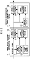
- Fig. 1 is a diagram showing a communication apparatus according to a first embodiment of the present invention.
- This communication apparatus is a digital coherent optical receiver which receives an optical signal transmitted from a transmission side.
- a local oscillation light source 1 (a local oscillator) is a light source which oscillates laser light with the same frequency as an optical signal. Due to an individual difference of the local oscillation light source 1, however, a frequency difference exists between a frequency of an optical signal and a frequency of output light of the local oscillation light source 1.
- An optical phase hybrid 2 mixes an optical signal and local light outputted from the local oscillation light source 1 to generate a pair of optical signals which are orthogonal to each other.
- One of the paired optical signals is obtained by combining the optical signal and the local light and is called an I (In-phase) component optical signal.
- the other of the paired optical signals is obtained by combining the optical signal and laser light obtained by rotating a phase of the local light by 90 degrees and is called a Q (Quadrature-phase, orthogonal) component optical signal.
- a photoelectric conversion portion 3 converts the pair of optical signals to a pair of analog electrical signals. That is, the photoelectric conversion portion 3 converts the I-component optical signal and the Q-component optical signal to an I-component electrical signal and a Q-component electrical signal.
- An AD (Analog to Digital) conversion portion 4 converts the pair of analog electrical signals to a pair of digital electrical signals by sampling the pair of analog electrical signals at a predetermined sampling frequency. That is, the AD conversion portion 4 converts the I-component analog electrical signal and the Q-component analog electrical signal to an I-component digital electrical signal and a Q-component digital electrical signal.
- a digital signal processing portion 5 restores (demodulates) transmit data by performing digital signal processing for the digital electrical signals outputted from the AD conversion portion 4.
- the digital signal processing portion 5 has a phase compensation device described below.
- Fig. 2 is a diagram showing a phase compensation device according to the first embodiment of the present invention.
- a known pattern is inserted into a data signal at predetermined intervals on a transmission side.
- the one or more symbols are simultaneously inserted at the same time into a plurality of data strings (physical lanes) which are simultaneously transmitted.
- data strings physical lanes
- one symbol is inserted.
- this will be referred to as a "short-cycle/short known pattern”. Therefore, the short-cycle/short known pattern is inserted into a received signal which is a digital electrical signal corresponding to an optical signal.
- a symbol phase difference compensating portion 6 calculates a first phase difference which is a phase difference between a short-cycle/short known pattern extracted from a received signal and a true value thereof and performs phase compensation for the received signal based on the first phase difference.
- a known pattern extracting portion 7 extracts a short-cycle/short known pattern inserted in a received signal.
- a true value of the short-cycle/short known pattern inserted into a data signal on a transmission side is stored in a reference signal storing portion 8 as a reference signal in advance.
- the phase of the reference signal indicates the phase which the short-cycle/short known pattern should originally take.
- a phase difference acquiring portion 9 acquires a first phase difference which is a phase difference between the short-cycle/short known pattern extracted by the known pattern extracting portion 7 and the reference signal.
- a phase difference compensating portion 10 performs phase compensation for the received signal based on the first phase difference. For example, phase rotation corresponding to the first phase difference is performed for the received signal.
- the phase compensation is not limited thereto. Calculation of electric field information may be performed to compensate the first phase difference by multiplication of an electric field vector.
- An output signal of the symbol phase difference compensating portion 6 is inputted to a tentative determination/phase compensation portion 11.
- a tentative determination portion 12 tentatively determines the output signal of the symbol phase difference compensating portion 6 to acquire an estimated value of a phase (a phase which originally should be taken).
- a phase difference acquiring portion 13 acquires a second phase difference which is a phase difference between a phase of the output signal of the symbol phase difference compensating portion 6 and the estimated value of the phase acquired by the tentative determination portion 12.
- a phase difference compensating portion 14 performs phase compensation for the output signal of the symbol phase difference compensating portion 6 based on the second phase difference.
- phase noise which cannot be sufficiently compensated by the symbol phase difference compensating portion 6 can be removed by the tentative determination/phase compensation portion 11.
- Each of the symbol phase difference compensating portion 6 and the tentative determination/phase compensation portion 11 has a simple feed-forward configuration. Furthermore, since most of phase noise is removed by the symbol phase difference compensating portion 6, it is not necessary to feed back a phase error before tentative determination. Therefore, it is possible to improve accuracy of phase fluctuation compensation without using a complicated feedback configuration.
- Fig. 3 is a diagram showing a phase compensation device according to a second embodiment of the present invention.
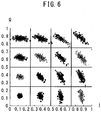
- Fig. 4 is a diagram in which output signals of the symbol phase difference compensating portion are plotted on a constellation.
- the constellation is also called a signal space diagram, and it is a diagram in which a digital modulation signal is expressed on a complex plane.
- the tentative determination portion 12 sets an estimated value of a phase for each of a plurality of threshold regions on the constellation, and determines estimated values of phases corresponding to threshold regions in which the output signals of the symbol phase difference compensating portion 6 are included.
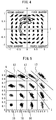
- Fig. 5 is a diagram showing a plurality of threshold regions set by the tentative determination portion according to the second embodiment of the present invention.
- Fig. 6 is a diagram showing a plurality of threshold regions set by a tentative determination portion according to a comparison example.
- all the plurality of threshold regions are in the same square shape and arranged in a checkerboard pattern.
- the plurality of threshold regions include a first threshold region 16 and a second threshold region 17 corresponding to signals whose amplitude is larger than that of signals to which the first threshold region 16 corresponds.
- the first threshold region 16 is in the same square shape and arranged in a checkerboard pattern.
- the second threshold region 17 extends in a phase rotation direction in comparison with the first threshold region 16. Since output signals of the symbol phase difference compensating portion 6 are spread and distributed in the phase rotation direction as the amplitude increases, it is possible to reduce error determination by setting threshold regions as in the present embodiment. Therefore, it becomes difficult to perform wrong phase compensation, and it is possible to reduce a phase compensation error.
- a complex conjugate portion 18 calculates complex conjugates of signals folded into the first quadrant.
- a multiplication portion 19 multiplying the complex conjugates by a signal outputted by the tentative determination portion 12, a complex signal of electric field information having phase differences among the signals is calculated.
- an amplitude standardizing portion 21 standardizes amplitudes to 1. This is for the purpose of preventing amplitudes of the output signals of the symbol phase difference compensating portion 6 from being influenced in the phase difference compensating portion 14.
- the phase difference compensating portion 14 multiplies the output signals of the symbol phase difference compensating portion 6 by the standardized complex signal. Thereby, for the output signals on which remaining phase noise exists, phase fluctuation can be compensated.
- a method of determining a moving average for every several symbols or a block averaging method of determining an average for each block can be used. Further, such a method can be also used that block averaging in which a moving average is determined for every half of a block and an interpolation function are combined.
- the determination can be performed by indicating a threshold by a threshold line on I and Q axes.
- the received signal (0.8, 0.9) exists in the determination region of the constellation (5/8, 7/8) and is data corresponding to (5/8, 7/8).
- the threshold lines can be indicated by quadratic curves. It is also possible to make the above variables A and B changeable. Furthermore, if the variables A and B can be set from outside, it is possible to change a threshold according to a reception situation.
- Fig. 8 is a diagram showing a phase compensation device according to a third embodiment of the present invention.
- a configuration until the multiplication portion 19 calculates a complex signal is similar to that of the second embodiment.
- a rotation angle calculating portion 22 calculates a rotation angle corresponding to a second phase difference ⁇ from the complex signal. Then, after the averaging portion 20 determines an average for several symbols, an exponential function display portion 23 shows the rotation angle by an exponential function expression EXPj ( ⁇ ).
- the phase difference compensating portion 14 multiplies output signals of the symbol phase difference compensating portion 6 by the rotation angle expressed by the exponential function expression. Thereby, for the output signals on which remaining phase noise exists, phase fluctuation can be compensated.
- a program for implementing the functions of the phase compensation device may be recorded in a computer-readable recording medium so that the program recorded in the recording medium is read in and executed by a computer system or a programmable logic device to perform phase compensation.
- the "computer system” described here may contain hardware such as OS, peripheral equipment, etc.
- the "computer system” may contain a WWW system having a homepage providing environment (or displaying environment).
- the "computer-readable recording medium” may be a portable medium such as a flexible disc, a magneto-optic disc, ROM and CD-ROM, or a storage device such as a hard disc incorporated in a computer system.
- the "computer-readable recording medium” may contain an element for holding a program for a constant time like a volatile memory (RAM) in a computer system serving as a server or a client when a program is transmitted through a network such as the Internet or a communication line such as a telephone line.
- the program may be transmitted from a computer system having a storage device or the like in which the program is stored, to another computer system via a transmission medium or by transmission waves in a transmission medium.
- the "transmission medium” for transmitting the program is a medium having a function of transmitting information like a network (communication network) such as the Internet or a communication circuit (communication line) such as a telephone line or the like.
- the program may be provided to perform a part of the foregoing function.
- the program may be provided to perform the foregoing function in combination with a program which has been already stored in the computer system, so-called a differential file (differentia program).
Applications Claiming Priority (2)
| Application Number | Priority Date | Filing Date | Title |
|---|---|---|---|
| JP2016120841A JP6183503B1 (ja) | 2016-06-17 | 2016-06-17 | 位相補償装置、位相補償方法及び通信装置 |
| PCT/JP2017/015195 WO2017217100A1 (ja) | 2016-06-17 | 2017-04-13 | 位相補償装置、位相補償方法及び通信装置 |
Publications (3)
| Publication Number | Publication Date |
|---|---|
| EP3402146A1 true EP3402146A1 (de) | 2018-11-14 |
| EP3402146A4 EP3402146A4 (de) | 2019-08-28 |
| EP3402146B1 EP3402146B1 (de) | 2020-10-07 |
Family
ID=59678252
Family Applications (1)
| Application Number | Title | Priority Date | Filing Date |
|---|---|---|---|
| EP17813006.8A Active EP3402146B1 (de) | 2016-06-17 | 2017-04-13 | Phasenkompensationsvorrichtung, phasenkompensationsverfahren und kommunikationsvorrichtung |
Country Status (6)
| Country | Link |
|---|---|
| US (1) | US10419127B2 (de) |
| EP (1) | EP3402146B1 (de) |
| JP (1) | JP6183503B1 (de) |
| CN (1) | CN109076040B (de) |
| CA (1) | CA3012977C (de) |
| WO (1) | WO2017217100A1 (de) |
Families Citing this family (5)
| Publication number | Priority date | Publication date | Assignee | Title |
|---|---|---|---|---|
| JP6288143B2 (ja) * | 2015-10-19 | 2018-03-07 | 日本電信電話株式会社 | コヒーレント光受信装置 |
| JP6743603B2 (ja) * | 2016-09-09 | 2020-08-19 | 富士通株式会社 | 受信装置及び位相誤差補償方法 |
| CN110460385B (zh) * | 2018-05-08 | 2022-05-31 | 富士通株式会社 | 相位噪声补偿装置及方法、接收机 |
| JP6627927B1 (ja) * | 2018-07-24 | 2020-01-08 | Nttエレクトロニクス株式会社 | 位相変動補償装置、位相変動補償方法及び通信装置 |
| WO2023119627A1 (ja) * | 2021-12-24 | 2023-06-29 | 日本電信電話株式会社 | 利得調整方法、光受信装置及びコンピュータプログラム |
Family Cites Families (13)
| Publication number | Priority date | Publication date | Assignee | Title |
|---|---|---|---|---|
| JPH09266499A (ja) * | 1996-01-26 | 1997-10-07 | Oki Electric Ind Co Ltd | デジタル復調回路、最大値検出回路及び受信装置 |
| US6647071B2 (en) * | 1998-11-06 | 2003-11-11 | Texas Instruments Incorporated | Method and apparatus for equalization and tracking of coded digital communications signals |
| US6928120B1 (en) | 2000-09-25 | 2005-08-09 | Cingular Wireless Ii, Llc | Methods and apparatus for use in reducing residual phase error in OFDM communication signals |
| JP4335121B2 (ja) * | 2004-11-11 | 2009-09-30 | 日本電信電話株式会社 | キャリア位相同期回路 |
| JP5046114B2 (ja) * | 2007-12-12 | 2012-10-10 | 日本電気株式会社 | 多値qam復調装置とその復調方法及び無線通信システム |
| US8340530B2 (en) * | 2009-03-10 | 2012-12-25 | Tyco Electronics Subsea Communications Llc | Local oscillator frequency offset compensation in a coherent optical signal receiver |
| CN103368882B (zh) * | 2012-04-10 | 2016-09-28 | 华为技术有限公司 | 一种相位噪声估计的方法及装置 |
| JP6126404B2 (ja) | 2013-02-13 | 2017-05-10 | 日本電信電話株式会社 | 送受信システム、及び通信方法 |
| WO2014126132A1 (ja) * | 2013-02-13 | 2014-08-21 | 日本電信電話株式会社 | 光伝送システム、位相補償方法、及び光受信装置 |
| JP6024531B2 (ja) * | 2013-03-12 | 2016-11-16 | 富士通株式会社 | 周波数誤差推定装置及び方法、周波数誤差補償装置、並びに、光受信機 |
| JP6131659B2 (ja) * | 2013-03-21 | 2017-05-24 | 富士通株式会社 | 光受信器および周波数オフセット補正方法 |
| JP6295585B2 (ja) * | 2013-10-09 | 2018-03-20 | 富士通株式会社 | 光通信受信装置、及び、周波数オフセット補償方法 |
| WO2015072515A1 (ja) * | 2013-11-15 | 2015-05-21 | 独立行政法人産業技術総合研究所 | 受信信号処理装置、通信システム及び受信信号処理方法 |
-
2016
- 2016-06-17 JP JP2016120841A patent/JP6183503B1/ja active Active
-
2017
- 2017-04-13 CN CN201780022063.9A patent/CN109076040B/zh active Active
- 2017-04-13 EP EP17813006.8A patent/EP3402146B1/de active Active
- 2017-04-13 US US16/072,420 patent/US10419127B2/en active Active
- 2017-04-13 WO PCT/JP2017/015195 patent/WO2017217100A1/ja active Application Filing
- 2017-04-13 CA CA3012977A patent/CA3012977C/en active Active
Also Published As
| Publication number | Publication date |
|---|---|
| CA3012977C (en) | 2021-05-11 |
| US20190074909A1 (en) | 2019-03-07 |
| CA3012977A1 (en) | 2017-12-21 |
| CN109076040A (zh) | 2018-12-21 |
| EP3402146B1 (de) | 2020-10-07 |
| JP2017225075A (ja) | 2017-12-21 |
| JP6183503B1 (ja) | 2017-08-23 |
| WO2017217100A1 (ja) | 2017-12-21 |
| CN109076040B (zh) | 2021-04-16 |
| EP3402146A4 (de) | 2019-08-28 |
| US10419127B2 (en) | 2019-09-17 |
Similar Documents
| Publication | Publication Date | Title |
|---|---|---|
| EP3402146B1 (de) | Phasenkompensationsvorrichtung, phasenkompensationsverfahren und kommunikationsvorrichtung | |
| JP6206545B1 (ja) | 伝送特性補償装置、伝送特性補償方法及び通信装置 | |
| CN102725960B (zh) | 用于相位和振荡器频率估计的方法 | |
| US8605828B2 (en) | Blind mechanism for demodulating offset QPSK signals in the presence of carrier phase error | |
| EP2501091A2 (de) | Quadraturmodulationssystem | |
| JP6743603B2 (ja) | 受信装置及び位相誤差補償方法 | |
| EP3029512A1 (de) | Spektralinversionsdetektion zur optischen Polarisierungsdivision-Multiplexübertragung | |
| US5854570A (en) | Feedback-free method for the demodulation of higher-level MQAM signals without knowledge of the transmitted symbols | |
| EP1279265A1 (de) | Blinde trägerverschiebungsdetektion für quadraturmodulierte digitale übertragungssysteme | |
| EP2779486B1 (de) | Frequenzfehlerschätzungsvorrichtung und -verfahren, Frequenzfehlerkompensierungsvorrichtung und optischer Empfänger | |
| CN116015590B (zh) | 一种信号的相位对齐方法、装置及相关设备 | |
| WO2020174656A1 (ja) | 受信信号処理装置、受信信号処理方法及び光受信器 | |
| US20230208528A1 (en) | Optical receiving device and clock synchronization method | |
| US11121778B1 (en) | Phase variation compensation device, phase variation compensation method and communication device | |
| JP7307391B2 (ja) | 光受信装置及び光受信方法 | |
| EP3866425B1 (de) | Empfangsvorrichtung, empfangsverfahren und programm | |
| JP6009953B2 (ja) | 光受信装置 | |
| JP6902259B2 (ja) | 測定装置及び測定方法 | |
| JP2015109576A (ja) | 光受信器および光信号受信方法 | |
| EP4315733A1 (de) | Verfahren und vorrichtung zur trägerrückgewinnung | |
| CN103326722B (zh) | 一种自适应样值估计电路和方法 | |
| EP2381596A1 (de) | Paralleler Digitalfilter | |
| KR20020095233A (ko) | 직교 변조식 디지털 통신 시스템을 위한 블라인드 검출방식의 반송파 오프셋 검출 방법 및 장치 |
Legal Events
| Date | Code | Title | Description |
|---|---|---|---|
| STAA | Information on the status of an ep patent application or granted ep patent |
Free format text: STATUS: THE INTERNATIONAL PUBLICATION HAS BEEN MADE |
|
| PUAI | Public reference made under article 153(3) epc to a published international application that has entered the european phase |
Free format text: ORIGINAL CODE: 0009012 |
|
| STAA | Information on the status of an ep patent application or granted ep patent |
Free format text: STATUS: REQUEST FOR EXAMINATION WAS MADE |
|
| 17P | Request for examination filed |
Effective date: 20180808 |
|
| AK | Designated contracting states |
Kind code of ref document: A1 Designated state(s): AL AT BE BG CH CY CZ DE DK EE ES FI FR GB GR HR HU IE IS IT LI LT LU LV MC MK MT NL NO PL PT RO RS SE SI SK SM TR |
|
| AX | Request for extension of the european patent |
Extension state: BA ME |
|
| A4 | Supplementary search report drawn up and despatched |
Effective date: 20190729 |
|
| RIC1 | Information provided on ipc code assigned before grant |
Ipc: H04B 10/61 20130101ALI20190723BHEP Ipc: H04L 27/01 20060101AFI20190723BHEP Ipc: H04L 27/00 20060101ALI20190723BHEP Ipc: H04L 27/38 20060101ALI20190723BHEP |
|
| DAV | Request for validation of the european patent (deleted) | ||
| DAX | Request for extension of the european patent (deleted) | ||
| STAA | Information on the status of an ep patent application or granted ep patent |
Free format text: STATUS: EXAMINATION IS IN PROGRESS |
|
| 17Q | First examination report despatched |
Effective date: 20191213 |
|
| GRAP | Despatch of communication of intention to grant a patent |
Free format text: ORIGINAL CODE: EPIDOSNIGR1 |
|
| STAA | Information on the status of an ep patent application or granted ep patent |
Free format text: STATUS: GRANT OF PATENT IS INTENDED |
|
| INTG | Intention to grant announced |
Effective date: 20200507 |
|
| GRAS | Grant fee paid |
Free format text: ORIGINAL CODE: EPIDOSNIGR3 |
|
| GRAA | (expected) grant |
Free format text: ORIGINAL CODE: 0009210 |
|
| STAA | Information on the status of an ep patent application or granted ep patent |
Free format text: STATUS: THE PATENT HAS BEEN GRANTED |
|
| AK | Designated contracting states |
Kind code of ref document: B1 Designated state(s): AL AT BE BG CH CY CZ DE DK EE ES FI FR GB GR HR HU IE IS IT LI LT LU LV MC MK MT NL NO PL PT RO RS SE SI SK SM TR |
|
| REG | Reference to a national code |
Ref country code: GB Ref legal event code: FG4D |
|
| REG | Reference to a national code |
Ref country code: CH Ref legal event code: EP Ref country code: AT Ref legal event code: REF Ref document number: 1322373 Country of ref document: AT Kind code of ref document: T Effective date: 20201015 |
|
| REG | Reference to a national code |
Ref country code: IE Ref legal event code: FG4D |
|
| REG | Reference to a national code |
Ref country code: DE Ref legal event code: R096 Ref document number: 602017025176 Country of ref document: DE |
|
| REG | Reference to a national code |
Ref country code: NL Ref legal event code: MP Effective date: 20201007 |
|
| REG | Reference to a national code |
Ref country code: AT Ref legal event code: MK05 Ref document number: 1322373 Country of ref document: AT Kind code of ref document: T Effective date: 20201007 |
|
| PG25 | Lapsed in a contracting state [announced via postgrant information from national office to epo] |
Ref country code: FI Free format text: LAPSE BECAUSE OF FAILURE TO SUBMIT A TRANSLATION OF THE DESCRIPTION OR TO PAY THE FEE WITHIN THE PRESCRIBED TIME-LIMIT Effective date: 20201007 Ref country code: PT Free format text: LAPSE BECAUSE OF FAILURE TO SUBMIT A TRANSLATION OF THE DESCRIPTION OR TO PAY THE FEE WITHIN THE PRESCRIBED TIME-LIMIT Effective date: 20210208 Ref country code: RS Free format text: LAPSE BECAUSE OF FAILURE TO SUBMIT A TRANSLATION OF THE DESCRIPTION OR TO PAY THE FEE WITHIN THE PRESCRIBED TIME-LIMIT Effective date: 20201007 Ref country code: GR Free format text: LAPSE BECAUSE OF FAILURE TO SUBMIT A TRANSLATION OF THE DESCRIPTION OR TO PAY THE FEE WITHIN THE PRESCRIBED TIME-LIMIT Effective date: 20210108 Ref country code: NO Free format text: LAPSE BECAUSE OF FAILURE TO SUBMIT A TRANSLATION OF THE DESCRIPTION OR TO PAY THE FEE WITHIN THE PRESCRIBED TIME-LIMIT Effective date: 20210107 |
|
| REG | Reference to a national code |
Ref country code: LT Ref legal event code: MG4D |
|
| PG25 | Lapsed in a contracting state [announced via postgrant information from national office to epo] |
Ref country code: BG Free format text: LAPSE BECAUSE OF FAILURE TO SUBMIT A TRANSLATION OF THE DESCRIPTION OR TO PAY THE FEE WITHIN THE PRESCRIBED TIME-LIMIT Effective date: 20210107 Ref country code: LV Free format text: LAPSE BECAUSE OF FAILURE TO SUBMIT A TRANSLATION OF THE DESCRIPTION OR TO PAY THE FEE WITHIN THE PRESCRIBED TIME-LIMIT Effective date: 20201007 Ref country code: PL Free format text: LAPSE BECAUSE OF FAILURE TO SUBMIT A TRANSLATION OF THE DESCRIPTION OR TO PAY THE FEE WITHIN THE PRESCRIBED TIME-LIMIT Effective date: 20201007 Ref country code: IS Free format text: LAPSE BECAUSE OF FAILURE TO SUBMIT A TRANSLATION OF THE DESCRIPTION OR TO PAY THE FEE WITHIN THE PRESCRIBED TIME-LIMIT Effective date: 20210207 Ref country code: SE Free format text: LAPSE BECAUSE OF FAILURE TO SUBMIT A TRANSLATION OF THE DESCRIPTION OR TO PAY THE FEE WITHIN THE PRESCRIBED TIME-LIMIT Effective date: 20201007 Ref country code: AT Free format text: LAPSE BECAUSE OF FAILURE TO SUBMIT A TRANSLATION OF THE DESCRIPTION OR TO PAY THE FEE WITHIN THE PRESCRIBED TIME-LIMIT Effective date: 20201007 Ref country code: ES Free format text: LAPSE BECAUSE OF FAILURE TO SUBMIT A TRANSLATION OF THE DESCRIPTION OR TO PAY THE FEE WITHIN THE PRESCRIBED TIME-LIMIT Effective date: 20201007 |
|
| PG25 | Lapsed in a contracting state [announced via postgrant information from national office to epo] |
Ref country code: NL Free format text: LAPSE BECAUSE OF FAILURE TO SUBMIT A TRANSLATION OF THE DESCRIPTION OR TO PAY THE FEE WITHIN THE PRESCRIBED TIME-LIMIT Effective date: 20201007 Ref country code: HR Free format text: LAPSE BECAUSE OF FAILURE TO SUBMIT A TRANSLATION OF THE DESCRIPTION OR TO PAY THE FEE WITHIN THE PRESCRIBED TIME-LIMIT Effective date: 20201007 |
|
| REG | Reference to a national code |
Ref country code: DE Ref legal event code: R097 Ref document number: 602017025176 Country of ref document: DE |
|
| PG25 | Lapsed in a contracting state [announced via postgrant information from national office to epo] |
Ref country code: SK Free format text: LAPSE BECAUSE OF FAILURE TO SUBMIT A TRANSLATION OF THE DESCRIPTION OR TO PAY THE FEE WITHIN THE PRESCRIBED TIME-LIMIT Effective date: 20201007 Ref country code: RO Free format text: LAPSE BECAUSE OF FAILURE TO SUBMIT A TRANSLATION OF THE DESCRIPTION OR TO PAY THE FEE WITHIN THE PRESCRIBED TIME-LIMIT Effective date: 20201007 Ref country code: LT Free format text: LAPSE BECAUSE OF FAILURE TO SUBMIT A TRANSLATION OF THE DESCRIPTION OR TO PAY THE FEE WITHIN THE PRESCRIBED TIME-LIMIT Effective date: 20201007 Ref country code: EE Free format text: LAPSE BECAUSE OF FAILURE TO SUBMIT A TRANSLATION OF THE DESCRIPTION OR TO PAY THE FEE WITHIN THE PRESCRIBED TIME-LIMIT Effective date: 20201007 Ref country code: CZ Free format text: LAPSE BECAUSE OF FAILURE TO SUBMIT A TRANSLATION OF THE DESCRIPTION OR TO PAY THE FEE WITHIN THE PRESCRIBED TIME-LIMIT Effective date: 20201007 Ref country code: SM Free format text: LAPSE BECAUSE OF FAILURE TO SUBMIT A TRANSLATION OF THE DESCRIPTION OR TO PAY THE FEE WITHIN THE PRESCRIBED TIME-LIMIT Effective date: 20201007 |
|
| PLBE | No opposition filed within time limit |
Free format text: ORIGINAL CODE: 0009261 |
|
| STAA | Information on the status of an ep patent application or granted ep patent |
Free format text: STATUS: NO OPPOSITION FILED WITHIN TIME LIMIT |
|
| PG25 | Lapsed in a contracting state [announced via postgrant information from national office to epo] |
Ref country code: DK Free format text: LAPSE BECAUSE OF FAILURE TO SUBMIT A TRANSLATION OF THE DESCRIPTION OR TO PAY THE FEE WITHIN THE PRESCRIBED TIME-LIMIT Effective date: 20201007 |
|
| 26N | No opposition filed |
Effective date: 20210708 |
|
| PG25 | Lapsed in a contracting state [announced via postgrant information from national office to epo] |
Ref country code: IT Free format text: LAPSE BECAUSE OF FAILURE TO SUBMIT A TRANSLATION OF THE DESCRIPTION OR TO PAY THE FEE WITHIN THE PRESCRIBED TIME-LIMIT Effective date: 20201007 Ref country code: AL Free format text: LAPSE BECAUSE OF FAILURE TO SUBMIT A TRANSLATION OF THE DESCRIPTION OR TO PAY THE FEE WITHIN THE PRESCRIBED TIME-LIMIT Effective date: 20201007 |
|
| PG25 | Lapsed in a contracting state [announced via postgrant information from national office to epo] |
Ref country code: MC Free format text: LAPSE BECAUSE OF FAILURE TO SUBMIT A TRANSLATION OF THE DESCRIPTION OR TO PAY THE FEE WITHIN THE PRESCRIBED TIME-LIMIT Effective date: 20201007 Ref country code: SI Free format text: LAPSE BECAUSE OF FAILURE TO SUBMIT A TRANSLATION OF THE DESCRIPTION OR TO PAY THE FEE WITHIN THE PRESCRIBED TIME-LIMIT Effective date: 20201007 |
|
| PG25 | Lapsed in a contracting state [announced via postgrant information from national office to epo] |
Ref country code: LU Free format text: LAPSE BECAUSE OF NON-PAYMENT OF DUE FEES Effective date: 20210413 |
|
| REG | Reference to a national code |
Ref country code: BE Ref legal event code: MM Effective date: 20210430 |
|
| PG25 | Lapsed in a contracting state [announced via postgrant information from national office to epo] |
Ref country code: CH Free format text: LAPSE BECAUSE OF NON-PAYMENT OF DUE FEES Effective date: 20210430 Ref country code: LI Free format text: LAPSE BECAUSE OF NON-PAYMENT OF DUE FEES Effective date: 20210430 |
|
| PG25 | Lapsed in a contracting state [announced via postgrant information from national office to epo] |
Ref country code: IE Free format text: LAPSE BECAUSE OF NON-PAYMENT OF DUE FEES Effective date: 20210413 |
|
| PG25 | Lapsed in a contracting state [announced via postgrant information from national office to epo] |
Ref country code: IS Free format text: LAPSE BECAUSE OF FAILURE TO SUBMIT A TRANSLATION OF THE DESCRIPTION OR TO PAY THE FEE WITHIN THE PRESCRIBED TIME-LIMIT Effective date: 20210207 |
|
| PG25 | Lapsed in a contracting state [announced via postgrant information from national office to epo] |
Ref country code: BE Free format text: LAPSE BECAUSE OF NON-PAYMENT OF DUE FEES Effective date: 20210430 |
|
| PGFP | Annual fee paid to national office [announced via postgrant information from national office to epo] |
Ref country code: FR Payment date: 20230309 Year of fee payment: 7 |
|
| PGFP | Annual fee paid to national office [announced via postgrant information from national office to epo] |
Ref country code: GB Payment date: 20230302 Year of fee payment: 7 |
|
| PG25 | Lapsed in a contracting state [announced via postgrant information from national office to epo] |
Ref country code: CY Free format text: LAPSE BECAUSE OF FAILURE TO SUBMIT A TRANSLATION OF THE DESCRIPTION OR TO PAY THE FEE WITHIN THE PRESCRIBED TIME-LIMIT Effective date: 20201007 |
|
| PG25 | Lapsed in a contracting state [announced via postgrant information from national office to epo] |
Ref country code: HU Free format text: LAPSE BECAUSE OF FAILURE TO SUBMIT A TRANSLATION OF THE DESCRIPTION OR TO PAY THE FEE WITHIN THE PRESCRIBED TIME-LIMIT; INVALID AB INITIO Effective date: 20170413 |
|
| PGFP | Annual fee paid to national office [announced via postgrant information from national office to epo] |
Ref country code: DE Payment date: 20230228 Year of fee payment: 7 |