EP3401970B1 - Herstellungsverfahren für eines quantenpunkt-leuchtdiodensubstrat - Google Patents
Herstellungsverfahren für eines quantenpunkt-leuchtdiodensubstrat Download PDFInfo
- Publication number
- EP3401970B1 EP3401970B1 EP16840275.8A EP16840275A EP3401970B1 EP 3401970 B1 EP3401970 B1 EP 3401970B1 EP 16840275 A EP16840275 A EP 16840275A EP 3401970 B1 EP3401970 B1 EP 3401970B1
- Authority
- EP
- European Patent Office
- Prior art keywords
- layer
- bonding layer
- light
- quantum dot
- quantum dots
- Prior art date
- Legal status (The legal status is an assumption and is not a legal conclusion. Google has not performed a legal analysis and makes no representation as to the accuracy of the status listed.)
- Active
Links
Images




Classifications
-
- H—ELECTRICITY
- H10—SEMICONDUCTOR DEVICES; ELECTRIC SOLID-STATE DEVICES NOT OTHERWISE PROVIDED FOR
- H10K—ORGANIC ELECTRIC SOLID-STATE DEVICES
- H10K50/00—Organic light-emitting devices
- H10K50/10—OLEDs or polymer light-emitting diodes [PLED]
- H10K50/11—OLEDs or polymer light-emitting diodes [PLED] characterised by the electroluminescent [EL] layers
- H10K50/115—OLEDs or polymer light-emitting diodes [PLED] characterised by the electroluminescent [EL] layers comprising active inorganic nanostructures, e.g. luminescent quantum dots
-
- B—PERFORMING OPERATIONS; TRANSPORTING
- B05—SPRAYING OR ATOMISING IN GENERAL; APPLYING FLUENT MATERIALS TO SURFACES, IN GENERAL
- B05D—PROCESSES FOR APPLYING FLUENT MATERIALS TO SURFACES, IN GENERAL
- B05D1/00—Processes for applying liquids or other fluent materials
- B05D1/002—Processes for applying liquids or other fluent materials the substrate being rotated
- B05D1/005—Spin coating
-
- H—ELECTRICITY
- H10—SEMICONDUCTOR DEVICES; ELECTRIC SOLID-STATE DEVICES NOT OTHERWISE PROVIDED FOR
- H10D—INORGANIC ELECTRIC SEMICONDUCTOR DEVICES
- H10D84/00—Integrated devices formed in or on semiconductor substrates that comprise only semiconducting layers, e.g. on Si wafers or on GaAs-on-Si wafers
- H10D84/01—Manufacture or treatment
-
- H—ELECTRICITY
- H10—SEMICONDUCTOR DEVICES; ELECTRIC SOLID-STATE DEVICES NOT OTHERWISE PROVIDED FOR
- H10K—ORGANIC ELECTRIC SOLID-STATE DEVICES
- H10K50/00—Organic light-emitting devices
- H10K50/10—OLEDs or polymer light-emitting diodes [PLED]
- H10K50/11—OLEDs or polymer light-emitting diodes [PLED] characterised by the electroluminescent [EL] layers
-
- H—ELECTRICITY
- H10—SEMICONDUCTOR DEVICES; ELECTRIC SOLID-STATE DEVICES NOT OTHERWISE PROVIDED FOR
- H10K—ORGANIC ELECTRIC SOLID-STATE DEVICES
- H10K50/00—Organic light-emitting devices
- H10K50/10—OLEDs or polymer light-emitting diodes [PLED]
- H10K50/11—OLEDs or polymer light-emitting diodes [PLED] characterised by the electroluminescent [EL] layers
- H10K50/125—OLEDs or polymer light-emitting diodes [PLED] characterised by the electroluminescent [EL] layers specially adapted for multicolour light emission, e.g. for emitting white light
-
- H—ELECTRICITY
- H10—SEMICONDUCTOR DEVICES; ELECTRIC SOLID-STATE DEVICES NOT OTHERWISE PROVIDED FOR
- H10K—ORGANIC ELECTRIC SOLID-STATE DEVICES
- H10K71/00—Manufacture or treatment specially adapted for the organic devices covered by this subclass
-
- H—ELECTRICITY
- H10—SEMICONDUCTOR DEVICES; ELECTRIC SOLID-STATE DEVICES NOT OTHERWISE PROVIDED FOR
- H10K—ORGANIC ELECTRIC SOLID-STATE DEVICES
- H10K2101/00—Properties of the organic materials covered by group H10K85/00
- H10K2101/40—Interrelation of parameters between multiple constituent active layers or sublayers, e.g. HOMO values in adjacent layers
-
- H—ELECTRICITY
- H10—SEMICONDUCTOR DEVICES; ELECTRIC SOLID-STATE DEVICES NOT OTHERWISE PROVIDED FOR
- H10K—ORGANIC ELECTRIC SOLID-STATE DEVICES
- H10K59/00—Integrated devices, or assemblies of multiple devices, comprising at least one organic light-emitting element covered by group H10K50/00
- H10K59/10—OLED displays
- H10K59/12—Active-matrix OLED [AMOLED] displays
-
- H—ELECTRICITY
- H10—SEMICONDUCTOR DEVICES; ELECTRIC SOLID-STATE DEVICES NOT OTHERWISE PROVIDED FOR
- H10K—ORGANIC ELECTRIC SOLID-STATE DEVICES
- H10K59/00—Integrated devices, or assemblies of multiple devices, comprising at least one organic light-emitting element covered by group H10K50/00
- H10K59/30—Devices specially adapted for multicolour light emission
- H10K59/35—Devices specially adapted for multicolour light emission comprising red-green-blue [RGB] subpixels
Definitions
- the present invention relates to a method of preparing a quantum dot light-emitting diode substrate having a bonding layer.
- AMOLED Active matrix organic light-emitting diode
- LCD liquid crystal display
- AMOLED products can hardly compete with LCD.
- the organic layer structure of an organic light-emitting display is typically prepared by a mask evaporation method which has disadvantages such as alignment difficulty, a low qualified product rate, incapacity to achieve luminescence of a smaller pixel area, and incapacity to accurately control the evaporation area, and thus cannot meet the increasing requirements for high-resolution display.
- Quantum dots also known as nanocrystals, are nanoparticles comprised of elements of Groups IIB and VIA or Groups IIIA and VA. Quantum dots generally have a particle size between 1 and 20 nm, and can emit fluorescence upon being exited as the continuous energy band structure is changed into a discrete energy level structure due to quantum confinement of electrons and holes.
- quantum efficiency has been improved to basically reach an industrialized level. It has become a trend to further adopt new techniques and processes to realize industrialization.
- US 2009/085473 A1 discloses a manufacturing method for an electroluminescent (EL) element, which can facilitate patterning for a luminescent layer containing quantum dots.
- the method includes: a wettability-changing-layer-forming step for forming a wettability changing layer containing a photocatalyst, on a substrate having a first electrode layer formed thereon, wherein wettability of the wettability-changing layer is changed by an effect of the photocatalyst associated with irradiation with energy; and a wettability-changing-pattern forming step for forming a wettability changing pattern composed of lyophilic regions and liquid-repellent regions, on a surface of the wettability changing layer, by irradiating the wettability changing layer with energy in a patterning manner.
- a luminescent layer is formed onto each lyophilic region, by coating a luminescentlayer-forming coating liquid containing the quantum dots, around each of which ligands are attached.
- US 2012/113672 A1 describes light-emitting quantum dot films, quantum dot lighting devices, and quantum dot-based backlight units, related compositions, components, and methods, and discloses quantum dot encapsulation and matrix materials, quantum dot films with protective barriers.
- WO 2005/055330 A1 discloses a matrix of EL organic material having quantum dots embedded therein. Electrodes provide electrons and holes to the matrix forming excitons to be transferred to the quantum dots. Transfer molecules on the quantum dots are facilitating the transfer of excitons from the EL organic material to the quantum dots, by first transferring them to the transfer molecules. The transfer molecules are chosen to make a transfer rate of excitons from the organic material to the transfer molecules larger than a decay rate of excitons in the organic material. More specifically, the organic matrix forms a light emitting layer in a light emitting device.
- the EL organic material is an EL polymer.
- US 2013/009131 A1 discloses a device including an emissive material comprising quantum dots.
- the device includes a first electrode and a second electrode, a layer comprising quantum dots disposed between the first electrode and the second electrodes, and a first interfacial layer disposed at the interface between a surface of the layer comprising quantum dots and a first layer in the device.
- a second interfacial layer is further disposed on the surface of the layer comprising quantum dots opposite to the first interfacial layer.
- the QD-LED substrate can be prepared with high resolution by a convenient process, and is suitable for mass production.
- the preparation method has an improved qualified product rate and is suitable for mass production.
- At least one embodiment not according to the present invention, provides a quantum dot light-emitting diode substrate, a display panel comprising the quantum dot light-emitting diode substrate, and the present invention provides a method of preparing the quantum dot light-emitting diode substrate.
- the quantum dot light-emitting diode substrate comprises a plurality of sub-pixel light-emitting regions, wherein each of the sub-pixel light-emitting regions comprises a light-emitting layer comprising a bonding layer and a quantum dot, the quantum dot being fixed in a corresponding sub-pixel light-emitting region by bonding to the bonding layer.
- the quantum dot light-emitting diode substrate can be prepared with high resolution by a convenient process, and is suitable for mass production.
- the preparation method has an improved qualified product rate and is suitable for mass production.
- the term "quantum dot light-emitting diode substrate" in the present application refers to a substrate comprising a light-emitting diode, wherein the light-emitting diode comprises a quantum dot configured to be capable of emitting light. Therefore, the light-emitting diode substrate in the present application can be an array substrate or a display substrate.
- organic functional group(s) of the quantum dot in the present application refers to organic functional group(s) or organic compound(s) present on the surface of the quantum dot and capable of undergoing a crosslinking reaction.
- organic functional group(s) of the bonding layer refers to organic functional group(s) or organic compound(s) present on the surface of the bonding layer and capable of undergoing a crosslinking reaction.
- the present embodiment provides a quantum dot light-emitting diode (QD-LED) substrate obtained by the method according to the claimed invention.
- the quantum dot light-emitting diode (QD-LED) substrate comprises a plurality of sub-pixel light-emitting regions 115 (e.g., red, green, blue (RGB) sub-pixels arranged in an array), wherein each of the sub-pixel light-emitting regions 115 comprises a light-emitting layer 114 comprising a bonding layer 106 and a quantum dot 113 bonded to the bonding layer 106.
- sub-pixel light-emitting regions 115 e.g., red, green, blue (RGB) sub-pixels arranged in an array
- each of the sub-pixel light-emitting regions 115 comprises a light-emitting layer 114 comprising a bonding layer 106 and a quantum dot 113 bonded to the bonding layer 106.
- the quantum dot 113 is not embedded in the bonding layer, for example, it is layered on the surface of the bonding layer.
- Each of the sub-pixel light-emitting regions 115 further comprises an electrode.
- the quantum dot 113 may comprise quantum dots of different colors, such as green light-emitting quantum dots, blue light-emitting quantum dots, and red light-emitting quantum dots.
- the present embodiment further provides a quantum dot light-emitting diode (QD-LED) substrate and a method of preparing the same.
- the quantum dot light-emitting diode (QD-LED) substrate comprises a plurality of sub-pixel light-emitting regions 115, wherein each of the sub-pixel light-emitting regions 115 comprises a light-emitting layer 114 comprising a bonding layer 106 and a quantum dot 113 bonded to the bonding layer 106.
- the quantum dot 113 is at least partially embedded in the bonding layer 106.
- the expression "the quantum dot is at least partially embedded in the bonding layer” means that each quantum dot is at least partially embedded in the bonding layer.
- Each of the sub-pixel light-emitting regions further comprises an electrode 102.
- the quantum dot may comprise quantum dots of different colors, such as green light-emitting quantum dots 107, blue light-emitting quantum dots 109, and red light-emitting quantum dots 111.
- the bonding layer 106 in the quantum dot light-emitting diode substrate comprises an organic resin.
- the bonding layer may be formed of an organic resin.
- the organic resin may comprise an organic resin material with conductor properties or semiconductor properties.
- the organic resin may be made conductive by adding thereto a conductive material such as carbon powder, or a conductive nano-metallic material such as a conductive nano-silver particle.
- the bonding layer 106 in the quantum dot light-emitting diode substrate is made of an organic semiconductor material or an organic conductor material.
- Organic semiconductors are organic materials having semiconductor properties (i.e., the electrical conductivity is between that of a metal and that of an insulator) and having a heat-activated conductivity between 10 -10 and 100 S ⁇ cm -1 .
- Organic semiconductors can be classified as organic small molecules, polymers and donor-receptor complexes.
- Organic small molecules include aromatic hydrocarbons, dyes, and organometallic compounds, such as purpurine, phthalocyanine, malachite green, rhodamine B and the like.
- Polymers include polymers with a saturated main chain and conjugated polymers, such as polyphenyl, polyacetylene, polyvinyl carbazole, polyphenylene sulfide and the like.
- Donor-receptor complexes consist of electron donors and electron acceptors, and a complex of tetramethyl-p-phenylenediamine and tetracyanoquinodimethane is a typical example of donor-receptor complexes.
- the conductivity type and conductivity of organic semiconductors can be modified by doping methods.
- the organic semiconductor can be doped with a conductive material such as carbon powder, or a conductive nano-metallic material such as a conductive nano-silver particle so that the organic semiconductor material will have good conductivity to become an organic conductor material.
- Organic conductor materials are organic compounds having conductivity, and include conductive polymer materials, and organic materials exhibiting conductor properties due to being doped with conductive materials.
- the organic resin in the quantum dot light-emitting diode substrate comprises an epoxy resin.
- Epoxy resins are a resin material which can be cured under conditions acceptable to a base substrate generally used without affecting the performance of other components on the base substrate, and can be modified in a variety of ways to adjust its conductivity.
- the bonding layer 106 and the quantum dot 113 in the quantum dot light-emitting diode substrate are bonded by forming a crosslinked network, wherein the quantum dot 113 forms a quantum dot layer. That is, the quantum dot layer is fixed by a crosslinked network formed by a crosslinking reaction of organic functional groups between the bonding layer 106 and the quantum dot 113.
- the quantum dot 113 in the quantum dot light-emitting diode substrate is bonded to the bonding layer 106 by being embedded in the bonding layer 106.
- the quantum dot 113 may be bonded to the bonding layer 106 on the surface of the bonding layer 106. The specific bonding manner depends on the condition applied.
- the quantum dot 113 is embedded in the bonding layer 106 and also crosslinked with the bonding layer 106 to form a crosslinked network.
- the light-emitting layer thus formed has a better bonding strength between the quantum dot and the bonding layer, which can ensure a high qualified product rate.
- the bonding layer 106 in the quantum dot light-emitting diode substrate has a thickness of about 5 to 50 nm, for example, 4.9 nm, and for another example, 51 nm.
- the bonding layer 106 has a thickness which is 0.8 to 2.0 times the size of the quantum dot particles, e.g., 1.0 to 1.1 times the size of the quantum dot particles.
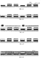
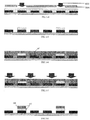
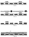
- FIG. 2-1 to FIG. 2-20 show a process for forming a bonding layer and a quantum dot layer by heating and/or pressing.
- the exemplary process is described below with reference to the accompanying drawings.
- a substrate 101 is provided, which is a base substrate.
- the base substrate is, for example, a glass substrate, a plastic substrate, or the like.
- an electrode material layer is formed on the substrate 101 and then patterned to obtain an electrode 102, which can be a cathode or an anode.
- an electrode 102 which can be a cathode or an anode.
- a switch element e.g., a thin film transistor
- a passivation layer or the like may be formed on the base substrate.
- a bonding layer material 103 is formed (for example, by coating or deposition) on the base substrate on which an electrode pattern has been formed.
- the bonding layer material 103 may be an organic semiconductor material or an organic conductor material.
- the bonding layer material 103 on the substrate 101 is patterned to form a bonding layer 106 corresponding to a pattern of a plurality of sub-pixel light-emitting regions.
- the bonding layer 106 is formed in the exposed region for example, after covering the unexposed region with a mask plate 104, irradiating the exposed region with ultraviolet light, and being developed.
- green quantum dots 107 are applied onto the bonding layer 106, the green quantum dots 107 are layered on the electrode 102 and the bonding layer 106 as well as the interval region therebetween.
- the green quantum dots 107 are bonded to the bonding layer 106 by external initiation conditions, such as heating, irradiation, or applying external pressure, or a combination thereof, so that the green quantum dots 107 are fixed in corresponding sub-pixel light-emitting regions.
- a pressurizer 116 is used in FIG. 2-7 to apply pressure to the quantum dots in the sub-pixel light-emitting regions.
- the methods of applying pressure are not limited to the above.
- pressure may also be applied by using a whole plate. The pressure applied may be such that the quantum dots are at least partially embedded in the bonding layer.
- the unbonded green quantum dots 107 are removed to form a green light-emitting layer 117 comprising a bonding layer 106 and a green quantum dot layer 108 bonded to the bonding layer 106, as shown in FIG. 2-8 .
- the quantum dots are partially or fully embedded in the bonding layer 106.
- the heating method may be partial heating or overall uniform heating, and the external pressure may be applied either locally or as a whole.
- FIG. 2-9 to FIG. 2-14 illustrate the process of forming a light-emitting layer comprising a bonding layer and a blue quantum dot layer 110 bonded to the bonding layer by a method of heating and applying external pressure. That is the process of repeating steps 2-3 to 2-8 except that blue quantum dots are used.
- a new bonding layer can be formed, for example, by a method of screen printing so that the position where the green quantum dot layer 108 has been formed is not covered by the new bonding layer; alternatively, a new bonding material can be formed on the entire substrate, and then the bonding material at the position where the green quantum dot layer 108 is formed is removed by patterning so as to form the bonding layer.
- a blue light-emitting layer 118 comprising a bonding layer and a blue quantum layer 110 bonded to the bonding layer is formed.
- FIG. 2-15 to FIG. 2-20 illustrate the process of forming a red quantum dot layer 112 by applying red quantum dots 111 by means of heating and applying external pressure. That is the process of repeating steps 2-3 to 2-8 except that red quantum dots are used.
- a new bonding layer may be formed, for example, by a screen printing method such that the position where the green quantum dot layer 108 or the blue quantum layer 110 has been formed is not covered by the new bonding layer; alternatively, a new bonding material may be formed on the entire substrate, and then the bonding material at the position where the green quantum dot layer 108 or the blue quantum layer 110 is formed is removed by patterning to form the bonding layer.
- a red light-emitting layer 119 comprising a bonding layer and a red quantum dot layer 112 bonded to the bonding layer is formed.
- the green light-emitting layer 117, the blue light-emitting layer 118 and the red light-emitting layer 119 are formed, and they are also not limited to the formation of the red, green and blue light-emitting layers.
- the green light-emitting layer 117, the blue light-emitting layer 118 and the red light-emitting layer 119 may be formed by quantum dots, while an organic light-emitting layer can be used for the other light-emitting layer(s).
- the external initiation condition can be selected from the group consisting of external thermal initiation, external pressure initiation, and combinations thereof
- the organic functional groups of the bonding layer 106 react with the organic functional groups of the quantum dot to form a crosslinked network taking a quantum dot inorganic core as the center.
- the quantum dot is bonded to the bonding layer 106 by being embedded in the bonding layer 106. It can be partially or fully embedded in the bonding layer 106, depending upon the external force and the property (for example, thickness) of the bonding layer.
- the bonding layer 106 has a thickness of about 5 to 50 nm.
- the bonding layer 106 is made of an organic semiconductor material or an organic conductor material.
- the bonding layer 106 formed only corresponds to a pattern of sub-pixel light-emitting regions with one color, and the method comprises repeating steps 2-3 to 2-8 several times so as to form a pattern of sub-pixel light-emitting regions with several colors.
- the bonding layer 106 formed corresponds to a pattern of sub-pixel light-emitting regions with at least two colors
- the method comprises forming a layer of a bonding material on a substrate only once, patterning the layer of the bonding material so as to form a bonding layer corresponding to a pattern of a plurality of sub-pixel light-emitting regions, and repeating the following process at least twice to form a pattern of sub-pixel light-emitting regions with at least two colors: applying a quantum dot onto the bonding layer; allowing the quantum dot to be bonded to the bonding layer by an external initiation condition so as to fix the quantum dot in a corresponding sub-pixel light-emitting region; and removing unbonded quantum dots to form a light-emitting layer comprising the bonding layer and quantum dots bonded to the bonding layer.
- the organic functional groups of the bonding layer react with the organic functional groups of the quantum dot to form a crosslinked network structure taking a quantum dot inorganic core as the center, thereby fixing the quantum dot in a corresponding sub-pixel region.
- the organic functional groups of the quantum dot may be one or more selected from the group consisting of: an organic functional group capable of undergoing a crosslinking reaction under light, an organic functional group capable of undergoing a crosslinking reaction at an elevated temperature, and an organic functional group capable of undergoing a crosslinking reaction under pressure.
- the organic functional groups in the bonding layer are functional groups capable of undergoing a crosslinking reaction with the functional groups of the quantum dot.
- the functional groups of the bonding layer material and the functional groups of the quantum dot are two different kinds of functional groups which are capable of reacting with each other under light (e.g., ultraviolet light, short wavelength visible light) to crosslink the quantum dots, thereby fixing the quantum dots.
- the functional groups can be selected from the group consisting of: alkenyl or dienyl such as 1,7-octadienyl, alkynyl or diynyl such as 1,9-octadiynyl, mercapto and the like.
- the functional groups of the bonding layer material and the functional groups of the quantum dot are two different kinds of functional groups which are capable of reacting with each other at a certain temperature, for example, at a temperature of 60°C to 400°, such as 90°C, 130°C, or 230°C, to crosslink the quantum dots, thereby fixing the quantum dots.
- the functional groups can be selected from the group consisting of: amino, pyridine and the like.
- the functional groups of the bonding layer material and the functional groups of the quantum dot are two different kinds of functional groups which are capable of reacting with each other under pressure to crosslink the quantum dots, thereby fixing the quantum dots.
- the bonding layer material may be an epoxy resin having a carboxylic group and comprise a material having functional groups which may undergo a crosslinking reaction, while the quantum dot may have a functional group such as thiol or phenol.
- the organic functional group(s) of the quantum dots are one or more selected from the group consisting of 1,7-octadiene, 1,9-octadiyne, mercapto, isoprene, amino, pyridine, carboxylic acid, thiol, phenol, or any combination thereof.
- the quantum dot light-emitting diode (QD-LED) substrate can be prepared with high resolution by a convenient process, and is suitable for mass production.
- the method of preparing the QD-LED substrate has an improved qualified product rate and is suitable for mass production.
- the present embodiment further illustrates a structure of a specific display panel and a method of preparing the same.
- the display panel comprises: a substrate, a TFT array, a cathode, an electron common layer, a bonding layer, a RGB (red, green, blue) three-color quantum dot sub-pixel, a hole common layer, an anode, a packaging material and an upper polarizing plate.
- the method of preparing the display panel is as follows.
- a transparent substrate was cleaned, and then the gate electrode metal Mo (with a thickness of 200 nm) was deposited and patterned; a gate electrode dielectric SiO 2 (with a thickness of 150 nm) was formed; an active layer IGZO (with a thickness of 40 nm) was formed and patterned; a source/drain electrode metal Mo (with a thickness of 200 nm) was formed and patterned; a passivation layer SiO 2 (with a thickness of 300 nm) was formed and patterned; a pixel electrode ITO (with a thickness of 40 nm) was formed and patterned; and finally an acrylic material was spin-coated and deposited, and then photolithographically etched and cured to form a pixel defining layer with a thickness of about 1.5 ⁇ m, thereby obtaining a TFT array portion. Afterwards, a flat layer could be formed on the TFT array.
- the surface of the substrate on which the TFT array was to be formed could be plasma-treated before the quantum dot light-emitting diode (QD-LED) portion was prepared.
- QD-LED quantum dot light-emitting diode
- a low work function metal was sputtered or vapor deposited as a cathode, followed by preparing an electron injection layer and an electron transport layer such as ZnO nanoparticles or LiF by spin-coating.
- a first layer of an epoxy resin bonding material was then applied, and the bonding material was retained in the green sub-pixel region by exposure, development and fixation to form a bonding layer used for green sub-pixels. Afterwards, a green quantum dot material was applied.
- the quantum dot material was synthesized by a traditional thermal injection method, where the ligands thereof include trioctylphosphine, trioctylphosphine oxide, oleylamine, oleic acid and the like. Afterwards, the epoxy resin was bonded to the quantum dot material at a temperature of 200°C and under a pressure of 0.5-5 Mpa, and was then developed and fixed to form a green sub-pixel.
- a second layer of the epoxy resin bonding material was applied, and the bonding material was retained in the blue sub-pixel region by exposure, development and fixation to form a bonding layer used for blue sub-pixels, and then a blue quantum dot material (which was synthesized by a traditional thermal injection method, and the ligands of which include trioctylphosphine, trioctylphosphine oxide, oleylamine, oleic acid and the like) was applied.
- a blue quantum dot material which was synthesized by a traditional thermal injection method, and the ligands of which include trioctylphosphine, trioctylphosphine oxide, oleylamine, oleic acid and the like
- the epoxy resin was bonded to the quantum dot material at a temperature of 200°C and under a pressure of 0.5-5 Mpa, and was then developed and fixed to form a blue sub-pixel; finally, a third layer of the epoxy resin bonding material was applied, and the bonding material was retained in the red sub-pixel region by exposure, development and fixation to form a bonding layer used for red sub-pixels, and then a red quantum dot material was applied.
- the epoxy resin was bonded to the quantum dot material at a temperature of 200°C and under a pressure of 0.5-5 Mpa, and was then developed and fixed to form a red sub-pixel.
- a second common layer (a hole injection layer and a hole transport layer) was spin-coated or vapor deposited, for example, PEDOT (poly(3,4-ethylenedioxythiophene)) : PSS (poly(styrenesulfonate)) and TFB (poly[(9,9-dioctylfluorenyl-2,7-diyl)-co-(4,4'-(N-(4-sec-butylphenyl)diphenylamine)]) were respectively spin-coated, wherein the hole injection layer and the hole transport layer have an entire thickness of about 50 to 100 nm; and finally, an anode metal thin layer was vapor deposited and sputtered, for example, by using an Au:ITO layer or the like, having a thickness of about 500-1000 nm. After vapor deposition, packaging and cutting were performed to obtain the panel portion of the Active Matrix - Quantum Dots - Light Emitting Diode (AM
- the manner of achieving elevated temperatures and pressures is not particularly limited, and a manner generally known to a person of ordinary skill in the art may be used.
- the heating temperature is achieved by heating a sample bearing bench (i.e., a bench with heating function), or by means of infrared radiation heating or the like.
- the method of applying pressure comprises applying pressure by rolling the roller and applying pressure using a flat plate or a patterned plate.
- the AM-QD-LED panel emits light in a top-emitting manner, and the minimum size of the sub-pixel that can be produced is about 10 to 30 nm, which is about 300 to 800 ppi.
- the present embodiment provides a quantum dot light-emitting diode (QD-LED) substrate, obtained by the method of the claimed invention, as shown in FIG. 1 , comprising a plurality of sub-pixel light-emitting regions 115, wherein each of the sub-pixel light-emitting regions comprises a light-emitting layer 114 comprising a bonding layer 106 and a quantum dot 113 bonded to the bonding layer 106.
- the quantum dot 113 is not embedded in the bonding layer and only exists on the surface of the bonding layer. In some embodiments, the quantum dot 113 is partially embedded in the bonding layer.
- Each of the sub-pixel light emitting regions 115 further comprises an electrode, and the quantum dot 113 comprises quantum dots of different colors, such as a green light-emitting quantum dot, a blue light-emitting quantum dot, a red light-emitting quantum dot, and the like.
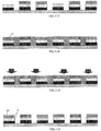
- FIG. 3-1 to FIG. 3-20 illustrate the process of preparing a QD-LED substrate which comprises bonding quantum dots to a bonding layer by ultraviolet light initiation.
- the light-emitting layer comprises a bonding layer and a quantum dot layer bonded to the bonding layer.
- Crosslink between the quantum dot layer and the bonding layer occurs on the bonding surface so as to form a crosslinked network.
- the quantum dots used in the present embodiment are photosensitive crosslinkable quantum dots having functional groups such as alkenyl, alkynyl or thiol capable of undergoing a crosslinking reaction.
- the organic functional group(s)of the quantum dots capable of reacting under light are one or more selected from the group consisting of 1,7-octadiene, 1,9-octadiyne, mercapto, isoprene or thiol.
- the bonding layer has functional groups, for example, alkenyl, dienyl, alkynyl, diynyl and the like, capable of undergoing a crosslinking reaction with the photosensitive crosslinkable quantum dots.
- Embodiment 1 is also applicable to Embodiment 2, unless contrary to the explicit teachings of Embodiment 2.
- a method of preparing the quantum dot light-emitting diode substrate is provided, as shown in FIG. 3-1 to FIG. 3-20 . It comprises subjecting the bonding layer and the quantum dot layer to a crosslinking reaction by ultraviolet light to form a crosslinked network taking a quantum dot inorganic core as the center, thereby forming a light-emitting layer.
- the exemplary process is described below with reference to the accompanying drawings.
- a substrate 101 is provided, which is a base substrate.
- an electrode material layer is formed on the substrate 101 and then patterned to obtain an electrode 102, which can be a cathode or an anode.
- an electrode 102 which can be a cathode or an anode.
- a switch element e.g., a thin film transistor
- a bonding layer material 103 is formed (for example, by coating or deposition) on the base substrate on which an electrode pattern has been formed.
- the bonding layer material 103 may be an organic semiconductor material or an organic conductor material.
- the bonding layer material 103 on the substrate 101 is patterned to form a bonding layer 106 corresponding to a pattern of a plurality of sub-pixel light-emitting regions.
- the bonding layer 106 is formed in the exposed region for example, after covering the unexposed region with a mask plate 104, irradiating the exposed region with ultraviolet light, and being developed.
- green quantum dots 107 are applied on the bonding layer 106, the green quantum dots 107 are layered on the electrode 102 and the bonding layer 106 as well as the interval region therebetween.
- the green quantum dots 107 and the bonding layer 106 are crosslinked by ultraviolet irradiation to form a crosslinked network taking a quantum dot inorganic core as the center, thereby fixing the green quantum dots 107 in a corresponding sub-pixel light-emitting region.
- the unbonded green quantum dots 107 are removed to form a green light-emitting layer 117 comprising a bonding layer 106 and a green quantum dot layer 108 bonded to the bonding layer 106, as shown in FIG. 3-8 .
- the quantum dots form a quantum dot layer on the surface of the bonding layer.
- FIG. 3-9 to FIG. 3-14 illustrate the process of forming a light-emitting layer comprising a bonding layer and a blue quantum dot layer 110 by a method of ultraviolet crosslinking. That is the process of repeating steps 3-3 to 3-8 except that blue crosslinkable quantum dots are used. As shown in FIG. 3-14 , a blue light-emitting layer 118 comprising a bonding layer and a blue quantum dot layer 110 bonded to the bonding layer is formed.
- FIG. 3-15 to FIG. 3-20 illustrate the process of forming a light-emitting layer comprising a bonding layer and a red quantum dot layer 112 by a method of ultraviolet crosslinking. That is the process of repeating steps 3-3 to 3-8 except that red crosslinkable quantum dots are used. As shown in FIG. 3-20 , a red light-emitting layer 119 comprising a bonding layer and a red quantum dot layer 112 bonded to the bonding layer is formed.
- the green light-emitting layer 117, the blue light-emitting layer 118 and the red light-emitting layer 119 are formed.
- the green light-emitting layer 117, the blue light-emitting layer 118 and the red light-emitting layer 119 may be formed by quantum dots, while an organic light-emitting layer can be used for the other light-emitting layer(s).
- the bonding layer 106 has a thickness of about 5 to 50 nm.
- the bonding layer 106 is made of an organic semiconductor material or an organic conductor material.
- the bonding layer 106 formed only corresponds to a pattern of sub-pixel light-emitting regions with one color, and the method comprises repeating steps 3-3 to 3-8 several times so as to form a pattern of sub-pixel light-emitting regions with several colors.
- the bonding layer 106 formed corresponds to a pattern of sub-pixel light-emitting regions with at least two colors
- the method comprises forming a layer of a bonding material on the substrate only once, patterning the layer of the bonding material so as to form a bonding layer corresponding to a pattern of a plurality of sub-pixel light-emitting regions, and repeating the following process at least twice to form a pattern of sub-pixel light-emitting regions with at least two colors: applying a quantum dot onto the bonding layer; allowing the quantum dot to be bonded to the bonding layer by an external initiation condition so as to fix the quantum dot in a corresponding sub-pixel light-emitting region; and removing unbonded quantum dots to form a light-emitting layer comprising the bonding layer and quantum dots bonded to the bonding layer.
- the external initiation condition is ultraviolet irradiation.
- the organic functional groups of the bonding layer react with the organic functional groups of the quantum dot to form a crosslinked network structure taking a quantum dot inorganic core as the center, thereby fixing the quantum dot in a corresponding sub-pixel region.
- the organic functional groups of the quantum dot may be one or more organic functional group(s) capable of undergoing a crosslinking reaction under light.
- the organic functional groups in the bonding layer are functional groups capable of undergoing a crosslinking reaction with the functional groups of the quantum dot.
- the functional groups of the bonding layer material and the functional groups of the quantum dot are two different kinds of functional groups which are capable of reacting with each other under light (e.g., ultraviolet light, short wavelength visible light) to crosslink quantum dots, thereby fixing the quantum dots.
- the functional groups can be selected from the group consisting of: dienyl such as 1,7-octadienyl, diynyl such as 1,9-octanediol, mercapto, isoprene and the like.
- the functional groups of the bonding layer material/the functional groups of the quantum dot may be configured, for example, as mercapto/alkenyl, mercapto/dienyl, mercapto/alkynyl, mercapto/diynyl, alkenyl/alkenyl, alkenyl/dienyl, and dienyl /dienyl.
- the organic functional group(s) of the quantum dots capable of reacting under light are one or more selected from the group consisting of 1,7-octadiene, 1,9-octadiyne, mercapto, isoprene or thiol.
- the quantum dot light-emitting diode (QD-LED) substrate can be prepared with high resolution by a convenient process, and is suitable for mass production.
- the method of preparing the QD-LED substrate has an improved qualified product rate and is suitable for mass production.
- the present embodiment further illustrates a structure of a specific display panel and a method of preparing the same.
- the display panel comprises: a substrate, a TFT array, a cathode, an electron common layer, a bonding layer, a red, green and blue three-color quantum dot sub-pixel, a hole common layer, an anode, a packaging material and an upper polarizing plate.
- the method of preparing the display panel is as follows.
- a transparent substrate was cleaned by a standard method, and then the gate electrode metal Mo (with a thickness of 200 nm) was deposited and patterned; a gate electrode dielectric SiO 2 (with a thickness of 150 nm) was formed; an active layer IGZO (with a thickness of 40 nm) was formed and patterned; a source/drain electrode metal Mo (with a thickness of 200 nm) was formed and patterned; a passivation layer SiO 2 (with a thickness of 300 nm) is formed and patterned; a pixel electrode ITO (with a thickness of 40 nm) was formed and patterned; and finally an acrylic material was spin-coated and deposited, and then photolithographically etched and cured to form a pixel defining layer with a thickness of about 1.5 ⁇ m, thereby obtaining a TFT backplate portion.
- Photosensitive crosslinkable quantum dots were prepared as follows.
- the quantum dot material was synthesized by a traditional thermal injection method, where the ligands thereof include trioctylphosphine, trioctylphosphine oxide, oleylamine, oleic acid, and the like.
- the green quantum dot material, the blue quantum dot material and the red quantum dot material were respectively contacted with a pyridine solvent at a weight ratio of 1:5 under stirring for 2 hours, so as to replace the ligands of the quantum dot material with pyridine.
- the quantum dots with a pyridine ligand were separated by centrifugation or the like.
- the quantum dots with a pyridine ligand were reacted with a crosslinkable ligand material (thioglycolic acid) having a monofunctional group to replace the pyridine ligand with a ligand having a monofunctional group, thereby obtaining monofunctional crosslinkable quantum dots (including: green photosensitive quantum dots, blue photosensitive quantum dots and red photosensitive quantum dots).
- the monofunctional crosslinkable quantum dots can react with a ligand having a plurality of alkenyl functional groups to form a crosslinked network.
- the backplate surface of TFT was plasma-treated before the QD-LED portion was prepared.
- a low work function metal was sputtered or vapor deposited as a cathode, followed by preparing an inorganic electron injection layer and an electron transport layer such as ZnO nanoparticles or LiF by spin-coating.
- a first layer of a negative photosensitive bonding material was then applied, and the bonding material was retained in the green sub-pixel region by exposure, development and fixation to form a bonding layer (the surface of the bonding layer has alkenyl functional groups) used for green sub-pixels. Afterwards, the green photosensitive quantum dot was applied.
- a third layer of the negative photosensitive bonding material was applied, and the bonding material was retained in the red sub-pixel region by exposure, development and fixation to form a bonding layer (the surface of the bonding layer has alkenyl functional groups) used for red sub-pixels.
- the red photosensitive quantum dot was applied. Overall exposure was performed using ultraviolet light, and then development and fixation were performed to form a red sub-pixel.
- a second common layer (a hole injection layer and a hole transport layer) was spin-coated or vapor deposited, for example, PEDOT:PSS and TFB were respectively spin-coated, wherein the hole injection layer and the hole transport layer have an entire thickness of about 50 to 100 nm; then, an anode metal thin layer was vapor deposited and sputtered, for example, by using an Au:ITO layer or the like, having a thickness of about 500-1000 nm. After vapor deposition, packaging and cutting were performed to obtain the entire display panel of the AM-QD-LED.
- the bonding materials for forming the bonding layer in the embodiments are not particularly limited as long as the object of the embodiments of the present invention can be achieved.
- the functional groups e.g., alkenyl, alkynyl and the like
- capable of undergoing a crosslinking reaction in the bonding layer can be formed by including a material having functional groups capable of undergoing a crosslinking reaction, such as a polybutadiene or styrene-maleic anhydride copolymer, in a bonding material, or by applying these materials on the surface of the bonding layer so that the surface of the bonding layer has functional groups capable of undergoing a crosslinking reaction.
- the bonding layer is formed of a polybutadiene or styrene-maleic anhydride copolymer.
- the AM-QD-LED panel emits light in a top-emitting manner, and the minimum size of the sub-pixel that can be produced is about 10 to 30 nm, which is about 300 to 800 ppi.
Landscapes
- Physics & Mathematics (AREA)
- Optics & Photonics (AREA)
- Engineering & Computer Science (AREA)
- Chemical & Material Sciences (AREA)
- Crystallography & Structural Chemistry (AREA)
- Inorganic Chemistry (AREA)
- Nanotechnology (AREA)
- Manufacturing & Machinery (AREA)
- Electroluminescent Light Sources (AREA)
Claims (8)
- Verfahren zur Herstellung eines lichtemittierenden Dioden-Substrats mit Quanten-Punkten, aufweisend:Schritt 1: Bilden einer Schicht (103) aus einem Bindematerial auf einem Substrat (101) und Strukturieren der Schicht aus dem Bindematerial, um eine Bindeschicht (106) zu bilden, die einer Struktur aus einer Vielzahl von lichtemittierenden Sub-Pixel-Bereichen entspricht;Schritt 2: Aufbringen einer kontinuierlichen Quanten-Punkt-Schicht (107), die Quanten-Punkte enthält, auf die Bindungsschicht;Schritt 3: Binden-lassen der Quanten-Punkte durch eine externe Aktivierungsbedingung (116) an die Bindungsschicht, um die Quanten-Punkte in einem entsprechenden lichtemittierenden Sub-Pixel-Bereich zu fixieren; undSchritt 4: Entfernen von ungebundenen Quanten-Punkten, um eine lichtemittierende Schicht (117) zu bilden, die die Bindungsschicht und an die Bindungsschicht gebundene Quanten-Punkte (108) aufweist;wobei die organische(n) funktionelle(n) Gruppe(n) der Bindungsschicht mit der (den) organischen funktionellen Gruppe(n) der Quanten-Punkte reagiert (reagieren), um ein vernetztes Netzwerk zu bilden, das einen anorganischen Quanten-Punkt-Kern als Zentrum nimmt, wodurch die Quanten-Punkte in einem entsprechenden lichtemittierenden Sub-Pixel-Bereich fixiert werden;
wobei die organische(n) funktionelle(n) Gruppe(n) der Quanten-Punkte eine oder mehrere ist/sind, die aus der Gruppe ausgewählt ist/sind, die aus 1,7-Octadien, 1,9-Octadin, Mercapto, Isopren, Amino, Pyridin, Carbonsäure, Thiol, Phenol oder einer Kombination davon besteht. - Verfahren nach Anspruch 1, wobei die externe Aktivierungsbedingung ausgewählt ist aus der Gruppe bestehend aus externer Photo-Aktivierung, externer thermischer Aktivierung, externer Druck-Aktivierung und Kombinationen davon.
- Verfahren nach Anspruch 1 oder 2, wobei das Bindematerial ein organisches Harz, vorzugsweise ein Epoxidharz, aufweist.
- Verfahren nach Anspruch 1 oder 2, wobei die Quanten-Punkte an die Bindungsschicht gebunden werden, indem sie in die Bindungsschicht eingebettet werden, und die Bindungsschicht eine Dicke von etwa 5 bis 50 Nanometern aufweist.
- Verfahren nach Anspruch 1 oder 2, wobei das Bindematerial ein organisches Halbleitermaterial, ein organisches Leitermaterial oder eine Kombination davon aufweist.
- Verfahren nach Anspruch 1 oder 2, wobeidie in Schritt 1 gebildete Verbindungsschicht nur eine Struktur von lichtemittierenden Sub-Pixel-Bereichen mit einer Farbe entspricht, unddas Verfahren aufweist: mehrmaliges Wiederholen der Schritte 1-4, um eine Struktur von lichtemittierenden Sub-Pixel-Bereichen mit mehreren Farben zu bilden.
- Verfahren nach Anspruch 1 oder 2, wobei das Verfahren aufweist:einmaliges Durchführen von Schritt 1, um die Verbindungsschicht zu bilden, die einer Struktur von lichtemittierenden Sub-Pixel-Bereichen mit mindestens zwei Farben entspricht, undmindestens zweimaliges Wiederholen der Schritte 2 bis 4, wodurch eine Struktur von lichtemittierenden Sub-Pixel-Bereichen mit mindestens zwei Farben gebildet wird.
- Verfahren nach Anspruch 1, wobei die organische(n) funktionelle(n) Gruppe(n) der Quanten-Punkte eine Vernetzungsreaktion unter Licht, eine Vernetzungsreaktion bei erhöhter Temperatur oder eine Vernetzungsreaktion unter Druck eingehen können.
Applications Claiming Priority (2)
| Application Number | Priority Date | Filing Date | Title |
|---|---|---|---|
| CN201610012450.1A CN105449111B (zh) | 2016-01-08 | 2016-01-08 | 具有结合层的量子点发光二极管基板及其制备方法 |
| PCT/CN2016/092849 WO2017117994A1 (zh) | 2016-01-08 | 2016-08-02 | 具有结合层的量子点发光二极管基板及其制备方法 |
Publications (3)
| Publication Number | Publication Date |
|---|---|
| EP3401970A1 EP3401970A1 (de) | 2018-11-14 |
| EP3401970A4 EP3401970A4 (de) | 2019-10-23 |
| EP3401970B1 true EP3401970B1 (de) | 2021-09-29 |
Family
ID=55559082
Family Applications (1)
| Application Number | Title | Priority Date | Filing Date |
|---|---|---|---|
| EP16840275.8A Active EP3401970B1 (de) | 2016-01-08 | 2016-08-02 | Herstellungsverfahren für eines quantenpunkt-leuchtdiodensubstrat |
Country Status (4)
| Country | Link |
|---|---|
| US (3) | US20180062101A1 (de) |
| EP (1) | EP3401970B1 (de) |
| CN (1) | CN105449111B (de) |
| WO (1) | WO2017117994A1 (de) |
Families Citing this family (42)
| Publication number | Priority date | Publication date | Assignee | Title |
|---|---|---|---|---|
| WO2016168151A1 (en) * | 2015-04-13 | 2016-10-20 | Carestream Health, Inc. | Reduction of tft instabiltity in digital x-ray detectors |
| CN105449111B (zh) * | 2016-01-08 | 2018-03-20 | 京东方科技集团股份有限公司 | 具有结合层的量子点发光二极管基板及其制备方法 |
| CN106129261B (zh) * | 2016-07-04 | 2019-09-17 | Tcl集团股份有限公司 | 一种量子点彩膜及其制备方法 |
| US10818856B2 (en) * | 2017-05-18 | 2020-10-27 | Shenzhen China Star Optoelectronics Semiconductor Display Technology Co., Ltd. | Method for fabricating thin film transistor, method for fabricating array substrate, and a display apparatus |
| CN107799672B (zh) * | 2017-10-30 | 2020-12-29 | 京东方科技集团股份有限公司 | 量子点层图案化的方法、量子点发光器件及其制作方法 |
| CN108172603A (zh) * | 2018-01-03 | 2018-06-15 | 京东方科技集团股份有限公司 | 一种量子点发光二极管基板及其制备方法、显示面板 |
| CN108447999B (zh) * | 2018-03-26 | 2021-04-30 | 京东方科技集团股份有限公司 | 量子点层图案化方法及显示装置的制作方法 |
| US10581007B2 (en) | 2018-03-27 | 2020-03-03 | Sharp Kabushiki Kaisha | Crosslinked emissive layer containing quantum dots for light-emitting device and method for making same |
| US10720591B2 (en) | 2018-03-27 | 2020-07-21 | Sharp Kabushiki Kaisha | Crosslinked emissive layer containing quantum dots for light-emitting device and method for making same |
| CN108511390B (zh) * | 2018-05-09 | 2020-07-07 | 广东普加福光电科技有限公司 | 一种量子点全彩微显示器件的制备方法 |
| TWI678009B (zh) * | 2018-06-22 | 2019-11-21 | 友達光電股份有限公司 | 顯示面板及其製作方法 |
| CN110718637B (zh) * | 2018-07-11 | 2020-12-22 | Tcl科技集团股份有限公司 | 一种量子点发光二极管及其制备方法 |
| WO2020041993A1 (zh) * | 2018-08-29 | 2020-03-05 | 华为技术有限公司 | 一种采用混合型发光二极管的显示屏幕及其制备方法 |
| CN109378395B (zh) * | 2018-10-18 | 2021-08-06 | 京东方科技集团股份有限公司 | 纳米粒子、显示基板的制备方法及显示装置 |
| CN109346506A (zh) * | 2018-10-25 | 2019-02-15 | 京东方科技集团股份有限公司 | 一种阵列基板及其制备方法、显示面板 |
| CN112970130B (zh) * | 2018-10-30 | 2024-02-09 | 夏普株式会社 | 发光元件、发光元件的制造方法 |
| CN110137387B (zh) * | 2019-05-16 | 2021-11-16 | 京东方科技集团股份有限公司 | 纳米粒子层图案化的方法、量子点发光器件及显示装置 |
| US10826011B1 (en) | 2019-07-23 | 2020-11-03 | Sharp Kabushiki Kaisha | QLED fabricated by patterning with phase separated emissive layer |
| CN112289960B (zh) * | 2019-07-25 | 2022-08-23 | Tcl科技集团股份有限公司 | 一种量子点发光二极管及其制备方法 |
| US12279503B2 (en) * | 2019-08-05 | 2025-04-15 | Sharp Kabushiki Kaisha | Display device and method of manufacturing display device |
| CN110707200B (zh) | 2019-09-04 | 2021-01-15 | 深圳市华星光电半导体显示技术有限公司 | 量子点发光器件图案化方法及量子点发光器件 |
| US12274114B2 (en) * | 2019-09-06 | 2025-04-08 | Sharp Kabushiki Kaisha | Display device including metal oxide nanoparticles for uniform and efficient lighting and method for producing same |
| CN110628417A (zh) * | 2019-09-27 | 2019-12-31 | 京东方科技集团股份有限公司 | 一种量子点配体及其制备方法、以及量子点膜及其制备方法 |
| WO2021070236A1 (ja) * | 2019-10-08 | 2021-04-15 | シャープ株式会社 | 発光デバイス |
| WO2021152790A1 (ja) * | 2020-01-30 | 2021-08-05 | シャープ株式会社 | 表示装置、および表示装置の製造方法 |
| US11309506B2 (en) | 2020-06-24 | 2022-04-19 | Sharp Kabushiki Kaisha | Light-emitting device with crosslinked emissive layer including quantum dots with ligands bonded thereto |
| US11309507B2 (en) | 2020-06-24 | 2022-04-19 | Sharp Kabushiki Kaisha | Control of the position of quantum dots in emissive layer of quantum dot light emitting diode |
| KR102806843B1 (ko) * | 2020-07-01 | 2025-05-12 | 삼성전자주식회사 | 발광 소자 및 이를 포함하는 표시 장치 |
| CN112271269B (zh) * | 2020-10-23 | 2024-02-13 | 京东方科技集团股份有限公司 | 显示面板及其制造方法 |
| CN114497410B (zh) * | 2020-10-27 | 2024-03-08 | 京东方科技集团股份有限公司 | 一种图案化量子点膜、量子点发光器件及制作方法 |
| CN112310330B (zh) | 2020-10-30 | 2024-06-04 | 北京京东方技术开发有限公司 | 一种量子点材料、量子点发光器件、显示装置及制作方法 |
| WO2022126442A1 (zh) * | 2020-12-16 | 2022-06-23 | 京东方科技集团股份有限公司 | 量子点层图案化的方法 |
| CN112750955A (zh) * | 2020-12-30 | 2021-05-04 | Tcl科技集团股份有限公司 | 一种量子点发光二极管及其制备方法 |
| CN114695708A (zh) * | 2020-12-31 | 2022-07-01 | Tcl科技集团股份有限公司 | 发光器件及其制备方法 |
| CN112916348B (zh) * | 2021-01-22 | 2022-05-17 | 中国计量大学 | 一种基于旋涂技术的可控量子点制备方法及量子点 |
| CN115244702B (zh) * | 2021-02-23 | 2025-03-11 | 京东方科技集团股份有限公司 | 量子点发光器件及其制作方法、显示装置 |
| CN113109974A (zh) * | 2021-03-25 | 2021-07-13 | 纳晶科技股份有限公司 | 一种量子点器件及其制备方法 |
| CN116349426A (zh) * | 2021-08-27 | 2023-06-27 | 京东方科技集团股份有限公司 | 发光器件及制备方法、显示面板和显示装置 |
| US12389744B2 (en) * | 2021-10-28 | 2025-08-12 | Samsung Electronics Co., Ltd. | Electroluminescent device, production method thereof, and display device including the same |
| WO2023155162A1 (zh) * | 2022-02-18 | 2023-08-24 | 京东方科技集团股份有限公司 | 显示基板、电致发光器件及其制备方法 |
| CN115172628B (zh) * | 2022-06-29 | 2026-01-16 | 北京京东方技术开发有限公司 | 经化学修饰的氧化石墨烯、显示装置及其制备方法 |
| CN115915827A (zh) * | 2022-10-08 | 2023-04-04 | 深圳市华星光电半导体显示技术有限公司 | 显示面板及其制作方法 |
Family Cites Families (15)
| Publication number | Priority date | Publication date | Assignee | Title |
|---|---|---|---|---|
| US20070077594A1 (en) * | 2003-12-02 | 2007-04-05 | Koninklijke Philips Electronics | Electroluminescent device |
| CN1960024B (zh) * | 2006-01-23 | 2010-08-11 | 邓先宇 | 电致发光聚合物全彩色显示器件的制作方法 |
| KR101296651B1 (ko) * | 2006-12-20 | 2013-08-14 | 엘지디스플레이 주식회사 | 유기전계발광 소자의 제조방법 |
| JP2009087781A (ja) * | 2007-09-28 | 2009-04-23 | Dainippon Printing Co Ltd | エレクトロルミネッセンス素子およびその製造方法 |
| KR100943839B1 (ko) * | 2007-10-31 | 2010-02-24 | 한국과학기술연구원 | 불규칙 표면구조의 우선 도입에 의해 고수율의바이오-이미지용 나노입자를 제조하는 방법 |
| US9525148B2 (en) * | 2008-04-03 | 2016-12-20 | Qd Vision, Inc. | Device including quantum dots |
| US8642991B2 (en) * | 2008-11-11 | 2014-02-04 | Samsung Electronics Co., Ltd. | Photosensitive quantum dot, composition comprising the same and method of forming quantum dot-containing pattern using the composition |
| KR101274068B1 (ko) * | 2010-05-25 | 2013-06-12 | 서울대학교산학협력단 | 양자점 발광 소자 및 이를 이용한 디스플레이 |
| US20130224282A1 (en) * | 2010-09-21 | 2013-08-29 | Massachusetts Institute Of Technology | Multistage Nanoparticles |
| EP3540300B1 (de) * | 2010-11-10 | 2024-05-08 | Shoei Chemical Inc. | Quantenpunktfilme, beleuchtungsvorrichtungen und beleuchtungsverfahren |
| US9425365B2 (en) * | 2012-08-20 | 2016-08-23 | Pacific Light Technologies Corp. | Lighting device having highly luminescent quantum dots |
| CN103226260B (zh) * | 2013-04-09 | 2015-12-09 | 北京京东方光电科技有限公司 | 液晶显示屏、显示装置及量子点层图形化的方法 |
| CN104536198A (zh) * | 2015-02-03 | 2015-04-22 | 京东方科技集团股份有限公司 | 一种显示基板、显示面板和显示装置 |
| CN105098075A (zh) * | 2015-07-14 | 2015-11-25 | Tcl集团股份有限公司 | 一种量子点发光层排布致密的发光器件及其制备方法 |
| CN105449111B (zh) * | 2016-01-08 | 2018-03-20 | 京东方科技集团股份有限公司 | 具有结合层的量子点发光二极管基板及其制备方法 |
-
2016
- 2016-01-08 CN CN201610012450.1A patent/CN105449111B/zh active Active
- 2016-08-02 US US15/508,663 patent/US20180062101A1/en not_active Abandoned
- 2016-08-02 WO PCT/CN2016/092849 patent/WO2017117994A1/zh not_active Ceased
- 2016-08-02 EP EP16840275.8A patent/EP3401970B1/de active Active
-
2019
- 2019-09-27 US US16/585,599 patent/US20200028106A1/en not_active Abandoned
-
2023
- 2023-03-10 US US18/119,894 patent/US20230232648A1/en not_active Abandoned
Also Published As
| Publication number | Publication date |
|---|---|
| US20230232648A1 (en) | 2023-07-20 |
| US20200028106A1 (en) | 2020-01-23 |
| CN105449111A (zh) | 2016-03-30 |
| CN105449111B (zh) | 2018-03-20 |
| EP3401970A1 (de) | 2018-11-14 |
| EP3401970A4 (de) | 2019-10-23 |
| WO2017117994A1 (zh) | 2017-07-13 |
| US20180062101A1 (en) | 2018-03-01 |
Similar Documents
| Publication | Publication Date | Title |
|---|---|---|
| US20230232648A1 (en) | Quantum dot light-emitting diode substrate having a bonding layer, and method of preparing the same | |
| US10224483B2 (en) | Crosslinkable quantum dot and preparing method thereof, array substrate and preparing method thereof | |
| CN105514302B (zh) | 量子点发光二极管亚像素阵列、其制造方法以及显示装置 | |
| JP5708482B2 (ja) | 有機電界発光装置,及び有機電界発光装置の製造方法 | |
| US20160036005A1 (en) | Display panel and display device | |
| EP3605612B1 (de) | Pixeldefinierende schicht, organische lichtemittierende vorrichtung und herstellungsverfahren dafür und anzeigevorrichtung | |
| US20090021153A1 (en) | Electroluminescent device and method for preparing the same | |
| WO2019061753A1 (zh) | 全溶液oled器件及其制作方法 | |
| US9484393B2 (en) | Array substrate of a display device, manufacturing method thereof | |
| CN107808897A (zh) | 一种有机发光二极管显示基板及其制作方法、显示装置 | |
| JP2009514178A (ja) | 構造化されたルミネセンス変換層 | |
| US20060152147A1 (en) | Electroluminescent device and method for preparing the same | |
| WO2020121398A1 (ja) | 表示装置およびその製造方法 | |
| US20150340416A1 (en) | Array substrate, method for producing the same and display apparatus | |
| KR101328577B1 (ko) | 편광 유기 발광 소자 및 그의 제조 방법 | |
| CN207068930U (zh) | Oled显示基板和oled显示装置 | |
| KR20130046435A (ko) | 유기 일렉트로루미네센스 소자 | |
| CN110828706A (zh) | 高分辨率Micro-OLED的制备方法以及显示模组 | |
| WO2020059024A1 (ja) | 発光素子、及び発光素子の製造方法 | |
| JP2011181304A (ja) | 有機el装置及びその製造方法 | |
| CN111564564A (zh) | 一种电致发光器件及其制备方法、显示装置及照明装置 | |
| CN113937242B (zh) | 一种超精细化量子点薄膜及其高分辨qled制备方法 | |
| CN207781600U (zh) | 一种有机发光二极管显示基板和显示装置 | |
| KR20080058141A (ko) | 유기전계발광 소자의 제조방법 | |
| US11785830B2 (en) | Method of manufacturing electroluminescent device having light emitting layer by using transfer printing process |
Legal Events
| Date | Code | Title | Description |
|---|---|---|---|
| STAA | Information on the status of an ep patent application or granted ep patent |
Free format text: STATUS: UNKNOWN |
|
| STAA | Information on the status of an ep patent application or granted ep patent |
Free format text: STATUS: THE INTERNATIONAL PUBLICATION HAS BEEN MADE |
|
| PUAI | Public reference made under article 153(3) epc to a published international application that has entered the european phase |
Free format text: ORIGINAL CODE: 0009012 |
|
| STAA | Information on the status of an ep patent application or granted ep patent |
Free format text: STATUS: REQUEST FOR EXAMINATION WAS MADE |
|
| 17P | Request for examination filed |
Effective date: 20170306 |
|
| AK | Designated contracting states |
Kind code of ref document: A1 Designated state(s): AL AT BE BG CH CY CZ DE DK EE ES FI FR GB GR HR HU IE IS IT LI LT LU LV MC MK MT NL NO PL PT RO RS SE SI SK SM TR |
|
| AX | Request for extension of the european patent |
Extension state: BA ME |
|
| DAV | Request for validation of the european patent (deleted) | ||
| DAX | Request for extension of the european patent (deleted) | ||
| RIN1 | Information on inventor provided before grant (corrected) |
Inventor name: ZHANG, YUANMING Inventor name: CHEN, ZHUO Inventor name: LEE, CHUNG CHUN Inventor name: LI, YANZHAO |
|
| A4 | Supplementary search report drawn up and despatched |
Effective date: 20190923 |
|
| RIC1 | Information provided on ipc code assigned before grant |
Ipc: H01L 27/32 20060101ALI20190917BHEP Ipc: H01L 51/50 20060101AFI20190917BHEP Ipc: H01L 51/56 20060101ALI20190917BHEP |
|
| GRAP | Despatch of communication of intention to grant a patent |
Free format text: ORIGINAL CODE: EPIDOSNIGR1 |
|
| STAA | Information on the status of an ep patent application or granted ep patent |
Free format text: STATUS: GRANT OF PATENT IS INTENDED |
|
| INTG | Intention to grant announced |
Effective date: 20210528 |
|
| GRAS | Grant fee paid |
Free format text: ORIGINAL CODE: EPIDOSNIGR3 |
|
| GRAA | (expected) grant |
Free format text: ORIGINAL CODE: 0009210 |
|
| STAA | Information on the status of an ep patent application or granted ep patent |
Free format text: STATUS: THE PATENT HAS BEEN GRANTED |
|
| AK | Designated contracting states |
Kind code of ref document: B1 Designated state(s): AL AT BE BG CH CY CZ DE DK EE ES FI FR GB GR HR HU IE IS IT LI LT LU LV MC MK MT NL NO PL PT RO RS SE SI SK SM TR |
|
| REG | Reference to a national code |
Ref country code: GB Ref legal event code: FG4D |
|
| REG | Reference to a national code |
Ref country code: CH Ref legal event code: EP Ref country code: AT Ref legal event code: REF Ref document number: 1434984 Country of ref document: AT Kind code of ref document: T Effective date: 20211015 |
|
| REG | Reference to a national code |
Ref country code: DE Ref legal event code: R096 Ref document number: 602016064440 Country of ref document: DE |
|
| REG | Reference to a national code |
Ref country code: IE Ref legal event code: FG4D |
|
| REG | Reference to a national code |
Ref country code: LT Ref legal event code: MG9D |
|
| PG25 | Lapsed in a contracting state [announced via postgrant information from national office to epo] |
Ref country code: SE Free format text: LAPSE BECAUSE OF FAILURE TO SUBMIT A TRANSLATION OF THE DESCRIPTION OR TO PAY THE FEE WITHIN THE PRESCRIBED TIME-LIMIT Effective date: 20210929 Ref country code: RS Free format text: LAPSE BECAUSE OF FAILURE TO SUBMIT A TRANSLATION OF THE DESCRIPTION OR TO PAY THE FEE WITHIN THE PRESCRIBED TIME-LIMIT Effective date: 20210929 Ref country code: LT Free format text: LAPSE BECAUSE OF FAILURE TO SUBMIT A TRANSLATION OF THE DESCRIPTION OR TO PAY THE FEE WITHIN THE PRESCRIBED TIME-LIMIT Effective date: 20210929 Ref country code: BG Free format text: LAPSE BECAUSE OF FAILURE TO SUBMIT A TRANSLATION OF THE DESCRIPTION OR TO PAY THE FEE WITHIN THE PRESCRIBED TIME-LIMIT Effective date: 20211229 Ref country code: NO Free format text: LAPSE BECAUSE OF FAILURE TO SUBMIT A TRANSLATION OF THE DESCRIPTION OR TO PAY THE FEE WITHIN THE PRESCRIBED TIME-LIMIT Effective date: 20211229 Ref country code: HR Free format text: LAPSE BECAUSE OF FAILURE TO SUBMIT A TRANSLATION OF THE DESCRIPTION OR TO PAY THE FEE WITHIN THE PRESCRIBED TIME-LIMIT Effective date: 20210929 Ref country code: FI Free format text: LAPSE BECAUSE OF FAILURE TO SUBMIT A TRANSLATION OF THE DESCRIPTION OR TO PAY THE FEE WITHIN THE PRESCRIBED TIME-LIMIT Effective date: 20210929 |
|
| REG | Reference to a national code |
Ref country code: NL Ref legal event code: MP Effective date: 20210929 |
|
| REG | Reference to a national code |
Ref country code: AT Ref legal event code: MK05 Ref document number: 1434984 Country of ref document: AT Kind code of ref document: T Effective date: 20210929 |
|
| PG25 | Lapsed in a contracting state [announced via postgrant information from national office to epo] |
Ref country code: LV Free format text: LAPSE BECAUSE OF FAILURE TO SUBMIT A TRANSLATION OF THE DESCRIPTION OR TO PAY THE FEE WITHIN THE PRESCRIBED TIME-LIMIT Effective date: 20210929 Ref country code: GR Free format text: LAPSE BECAUSE OF FAILURE TO SUBMIT A TRANSLATION OF THE DESCRIPTION OR TO PAY THE FEE WITHIN THE PRESCRIBED TIME-LIMIT Effective date: 20211230 |
|
| PG25 | Lapsed in a contracting state [announced via postgrant information from national office to epo] |
Ref country code: AT Free format text: LAPSE BECAUSE OF FAILURE TO SUBMIT A TRANSLATION OF THE DESCRIPTION OR TO PAY THE FEE WITHIN THE PRESCRIBED TIME-LIMIT Effective date: 20210929 |
|
| PG25 | Lapsed in a contracting state [announced via postgrant information from national office to epo] |
Ref country code: IS Free format text: LAPSE BECAUSE OF FAILURE TO SUBMIT A TRANSLATION OF THE DESCRIPTION OR TO PAY THE FEE WITHIN THE PRESCRIBED TIME-LIMIT Effective date: 20220129 Ref country code: SK Free format text: LAPSE BECAUSE OF FAILURE TO SUBMIT A TRANSLATION OF THE DESCRIPTION OR TO PAY THE FEE WITHIN THE PRESCRIBED TIME-LIMIT Effective date: 20210929 Ref country code: RO Free format text: LAPSE BECAUSE OF FAILURE TO SUBMIT A TRANSLATION OF THE DESCRIPTION OR TO PAY THE FEE WITHIN THE PRESCRIBED TIME-LIMIT Effective date: 20210929 Ref country code: PT Free format text: LAPSE BECAUSE OF FAILURE TO SUBMIT A TRANSLATION OF THE DESCRIPTION OR TO PAY THE FEE WITHIN THE PRESCRIBED TIME-LIMIT Effective date: 20220131 Ref country code: PL Free format text: LAPSE BECAUSE OF FAILURE TO SUBMIT A TRANSLATION OF THE DESCRIPTION OR TO PAY THE FEE WITHIN THE PRESCRIBED TIME-LIMIT Effective date: 20210929 Ref country code: NL Free format text: LAPSE BECAUSE OF FAILURE TO SUBMIT A TRANSLATION OF THE DESCRIPTION OR TO PAY THE FEE WITHIN THE PRESCRIBED TIME-LIMIT Effective date: 20210929 Ref country code: ES Free format text: LAPSE BECAUSE OF FAILURE TO SUBMIT A TRANSLATION OF THE DESCRIPTION OR TO PAY THE FEE WITHIN THE PRESCRIBED TIME-LIMIT Effective date: 20210929 Ref country code: EE Free format text: LAPSE BECAUSE OF FAILURE TO SUBMIT A TRANSLATION OF THE DESCRIPTION OR TO PAY THE FEE WITHIN THE PRESCRIBED TIME-LIMIT Effective date: 20210929 Ref country code: CZ Free format text: LAPSE BECAUSE OF FAILURE TO SUBMIT A TRANSLATION OF THE DESCRIPTION OR TO PAY THE FEE WITHIN THE PRESCRIBED TIME-LIMIT Effective date: 20210929 Ref country code: AL Free format text: LAPSE BECAUSE OF FAILURE TO SUBMIT A TRANSLATION OF THE DESCRIPTION OR TO PAY THE FEE WITHIN THE PRESCRIBED TIME-LIMIT Effective date: 20210929 |
|
| REG | Reference to a national code |
Ref country code: DE Ref legal event code: R097 Ref document number: 602016064440 Country of ref document: DE |
|
| PG25 | Lapsed in a contracting state [announced via postgrant information from national office to epo] |
Ref country code: DK Free format text: LAPSE BECAUSE OF FAILURE TO SUBMIT A TRANSLATION OF THE DESCRIPTION OR TO PAY THE FEE WITHIN THE PRESCRIBED TIME-LIMIT Effective date: 20210929 |
|
| PLBE | No opposition filed within time limit |
Free format text: ORIGINAL CODE: 0009261 |
|
| STAA | Information on the status of an ep patent application or granted ep patent |
Free format text: STATUS: NO OPPOSITION FILED WITHIN TIME LIMIT |
|
| 26N | No opposition filed |
Effective date: 20220630 |
|
| REG | Reference to a national code |
Ref country code: DE Ref legal event code: R079 Ref document number: 602016064440 Country of ref document: DE Free format text: PREVIOUS MAIN CLASS: H01L0051500000 Ipc: H10K0050000000 |
|
| PG25 | Lapsed in a contracting state [announced via postgrant information from national office to epo] |
Ref country code: SI Free format text: LAPSE BECAUSE OF FAILURE TO SUBMIT A TRANSLATION OF THE DESCRIPTION OR TO PAY THE FEE WITHIN THE PRESCRIBED TIME-LIMIT Effective date: 20210929 |
|
| PG25 | Lapsed in a contracting state [announced via postgrant information from national office to epo] |
Ref country code: IT Free format text: LAPSE BECAUSE OF FAILURE TO SUBMIT A TRANSLATION OF THE DESCRIPTION OR TO PAY THE FEE WITHIN THE PRESCRIBED TIME-LIMIT Effective date: 20210929 |
|
| PG25 | Lapsed in a contracting state [announced via postgrant information from national office to epo] |
Ref country code: MC Free format text: LAPSE BECAUSE OF FAILURE TO SUBMIT A TRANSLATION OF THE DESCRIPTION OR TO PAY THE FEE WITHIN THE PRESCRIBED TIME-LIMIT Effective date: 20210929 |
|
| REG | Reference to a national code |
Ref country code: CH Ref legal event code: PL |
|
| GBPC | Gb: european patent ceased through non-payment of renewal fee |
Effective date: 20220802 |
|
| PG25 | Lapsed in a contracting state [announced via postgrant information from national office to epo] |
Ref country code: LU Free format text: LAPSE BECAUSE OF NON-PAYMENT OF DUE FEES Effective date: 20220802 Ref country code: LI Free format text: LAPSE BECAUSE OF NON-PAYMENT OF DUE FEES Effective date: 20220831 Ref country code: CH Free format text: LAPSE BECAUSE OF NON-PAYMENT OF DUE FEES Effective date: 20220831 |
|
| REG | Reference to a national code |
Ref country code: BE Ref legal event code: MM Effective date: 20220831 |
|
| PG25 | Lapsed in a contracting state [announced via postgrant information from national office to epo] |
Ref country code: IE Free format text: LAPSE BECAUSE OF NON-PAYMENT OF DUE FEES Effective date: 20220802 Ref country code: FR Free format text: LAPSE BECAUSE OF NON-PAYMENT OF DUE FEES Effective date: 20220831 |
|
| PG25 | Lapsed in a contracting state [announced via postgrant information from national office to epo] |
Ref country code: BE Free format text: LAPSE BECAUSE OF NON-PAYMENT OF DUE FEES Effective date: 20220831 |
|
| PG25 | Lapsed in a contracting state [announced via postgrant information from national office to epo] |
Ref country code: GB Free format text: LAPSE BECAUSE OF NON-PAYMENT OF DUE FEES Effective date: 20220802 |
|
| PG25 | Lapsed in a contracting state [announced via postgrant information from national office to epo] |
Ref country code: HU Free format text: LAPSE BECAUSE OF FAILURE TO SUBMIT A TRANSLATION OF THE DESCRIPTION OR TO PAY THE FEE WITHIN THE PRESCRIBED TIME-LIMIT; INVALID AB INITIO Effective date: 20160802 |
|
| PG25 | Lapsed in a contracting state [announced via postgrant information from national office to epo] |
Ref country code: SM Free format text: LAPSE BECAUSE OF FAILURE TO SUBMIT A TRANSLATION OF THE DESCRIPTION OR TO PAY THE FEE WITHIN THE PRESCRIBED TIME-LIMIT Effective date: 20210929 Ref country code: MK Free format text: LAPSE BECAUSE OF FAILURE TO SUBMIT A TRANSLATION OF THE DESCRIPTION OR TO PAY THE FEE WITHIN THE PRESCRIBED TIME-LIMIT Effective date: 20210929 Ref country code: CY Free format text: LAPSE BECAUSE OF FAILURE TO SUBMIT A TRANSLATION OF THE DESCRIPTION OR TO PAY THE FEE WITHIN THE PRESCRIBED TIME-LIMIT Effective date: 20210929 |
|
| PG25 | Lapsed in a contracting state [announced via postgrant information from national office to epo] |
Ref country code: MT Free format text: LAPSE BECAUSE OF FAILURE TO SUBMIT A TRANSLATION OF THE DESCRIPTION OR TO PAY THE FEE WITHIN THE PRESCRIBED TIME-LIMIT Effective date: 20210929 |
|
| PGFP | Annual fee paid to national office [announced via postgrant information from national office to epo] |
Ref country code: DE Payment date: 20250819 Year of fee payment: 10 |
|
| PG25 | Lapsed in a contracting state [announced via postgrant information from national office to epo] |
Ref country code: TR Free format text: LAPSE BECAUSE OF FAILURE TO SUBMIT A TRANSLATION OF THE DESCRIPTION OR TO PAY THE FEE WITHIN THE PRESCRIBED TIME-LIMIT Effective date: 20210929 |