EP3398953B1 - Organische elektrolumineszente materialien und vorrichtungen - Google Patents
Organische elektrolumineszente materialien und vorrichtungen Download PDFInfo
- Publication number
- EP3398953B1 EP3398953B1 EP18170637.5A EP18170637A EP3398953B1 EP 3398953 B1 EP3398953 B1 EP 3398953B1 EP 18170637 A EP18170637 A EP 18170637A EP 3398953 B1 EP3398953 B1 EP 3398953B1
- Authority
- EP
- European Patent Office
- Prior art keywords
- group
- compound
- formula
- ring
- ligand
- Prior art date
- Legal status (The legal status is an assumption and is not a legal conclusion. Google has not performed a legal analysis and makes no representation as to the accuracy of the status listed.)
- Active
Links
- 239000000463 material Substances 0.000 title description 79
- 239000010410 layer Substances 0.000 claims description 88
- 150000001875 compounds Chemical class 0.000 claims description 84
- -1 amino, silyl Chemical group 0.000 claims description 64
- 125000003118 aryl group Chemical group 0.000 claims description 61
- 239000003446 ligand Substances 0.000 claims description 55
- IJGRMHOSHXDMSA-UHFFFAOYSA-N Atomic nitrogen Chemical compound N#N IJGRMHOSHXDMSA-UHFFFAOYSA-N 0.000 claims description 46
- 125000001072 heteroaryl group Chemical group 0.000 claims description 44
- 125000000217 alkyl group Chemical group 0.000 claims description 40
- 125000000753 cycloalkyl group Chemical group 0.000 claims description 37
- 229910052751 metal Inorganic materials 0.000 claims description 34
- 239000002184 metal Substances 0.000 claims description 33
- 229910052757 nitrogen Inorganic materials 0.000 claims description 32
- 125000003342 alkenyl group Chemical group 0.000 claims description 30
- 125000000392 cycloalkenyl group Chemical group 0.000 claims description 28
- 125000003545 alkoxy group Chemical group 0.000 claims description 27
- 125000004404 heteroalkyl group Chemical group 0.000 claims description 27
- 125000004104 aryloxy group Chemical group 0.000 claims description 26
- 150000002527 isonitriles Chemical group 0.000 claims description 26
- 150000002825 nitriles Chemical group 0.000 claims description 26
- 239000002019 doping agent Substances 0.000 claims description 23
- 125000000304 alkynyl group Chemical group 0.000 claims description 19
- 125000003710 aryl alkyl group Chemical group 0.000 claims description 19
- 239000012044 organic layer Substances 0.000 claims description 19
- 238000006467 substitution reaction Methods 0.000 claims description 19
- YZCKVEUIGOORGS-OUBTZVSYSA-N Deuterium Chemical compound [2H] YZCKVEUIGOORGS-OUBTZVSYSA-N 0.000 claims description 17
- 229910052805 deuterium Inorganic materials 0.000 claims description 17
- 229910052739 hydrogen Inorganic materials 0.000 claims description 16
- 239000001257 hydrogen Substances 0.000 claims description 16
- 125000002252 acyl group Chemical group 0.000 claims description 15
- 125000002915 carbonyl group Chemical group [*:2]C([*:1])=O 0.000 claims description 15
- 150000002148 esters Chemical group 0.000 claims description 15
- FVZVCSNXTFCBQU-UHFFFAOYSA-N phosphanyl Chemical group [PH2] FVZVCSNXTFCBQU-UHFFFAOYSA-N 0.000 claims description 15
- 125000000475 sulfinyl group Chemical group [*:2]S([*:1])=O 0.000 claims description 15
- 125000000472 sulfonyl group Chemical group *S(*)(=O)=O 0.000 claims description 15
- 125000003396 thiol group Chemical group [H]S* 0.000 claims description 15
- 150000001735 carboxylic acids Chemical group 0.000 claims description 14
- 150000002431 hydrogen Chemical class 0.000 claims description 14
- 125000004432 carbon atom Chemical group C* 0.000 claims description 12
- 125000000623 heterocyclic group Chemical group 0.000 claims description 12
- 229910052760 oxygen Inorganic materials 0.000 claims description 12
- 229910052799 carbon Inorganic materials 0.000 claims description 10
- 150000004820 halides Chemical class 0.000 claims description 10
- OKTJSMMVPCPJKN-UHFFFAOYSA-N Carbon Chemical compound [C] OKTJSMMVPCPJKN-UHFFFAOYSA-N 0.000 claims description 9
- 229910052717 sulfur Inorganic materials 0.000 claims description 8
- 125000001054 5 membered carbocyclic group Chemical group 0.000 claims description 7
- 125000004008 6 membered carbocyclic group Chemical group 0.000 claims description 7
- 230000003647 oxidation Effects 0.000 claims description 6
- 238000007254 oxidation reaction Methods 0.000 claims description 6
- 125000006413 ring segment Chemical group 0.000 claims description 6
- 229910052741 iridium Inorganic materials 0.000 claims description 5
- 229910052697 platinum Inorganic materials 0.000 claims description 4
- 229910052762 osmium Inorganic materials 0.000 claims description 3
- 229910052802 copper Inorganic materials 0.000 claims description 2
- 125000002147 dimethylamino group Chemical group [H]C([H])([H])N(*)C([H])([H])[H] 0.000 claims description 2
- 229910052737 gold Inorganic materials 0.000 claims description 2
- 229910052702 rhenium Inorganic materials 0.000 claims description 2
- 229910052703 rhodium Inorganic materials 0.000 claims description 2
- 229910052707 ruthenium Inorganic materials 0.000 claims description 2
- 229910052711 selenium Inorganic materials 0.000 claims description 2
- 0 C*1CCCCC1 Chemical compound C*1CCCCC1 0.000 description 48
- XEKOWRVHYACXOJ-UHFFFAOYSA-N Ethyl acetate Chemical compound CCOC(C)=O XEKOWRVHYACXOJ-UHFFFAOYSA-N 0.000 description 26
- 239000000203 mixture Substances 0.000 description 21
- 239000000047 product Substances 0.000 description 19
- 125000001424 substituent group Chemical group 0.000 description 18
- YMWUJEATGCHHMB-UHFFFAOYSA-N dichloromethane Natural products ClCCl YMWUJEATGCHHMB-UHFFFAOYSA-N 0.000 description 16
- UHOVQNZJYSORNB-UHFFFAOYSA-N Benzene Chemical compound C1=CC=CC=C1 UHOVQNZJYSORNB-UHFFFAOYSA-N 0.000 description 15
- UJOBWOGCFQCDNV-UHFFFAOYSA-N 9H-carbazole Chemical compound C1=CC=C2C3=CC=CC=C3NC2=C1 UJOBWOGCFQCDNV-UHFFFAOYSA-N 0.000 description 14
- TXCDCPKCNAJMEE-UHFFFAOYSA-N dibenzofuran Chemical compound C1=CC=C2C3=CC=CC=C3OC2=C1 TXCDCPKCNAJMEE-UHFFFAOYSA-N 0.000 description 14
- 239000000243 solution Substances 0.000 description 14
- 235000019439 ethyl acetate Nutrition 0.000 description 13
- OKKJLVBELUTLKV-UHFFFAOYSA-N Methanol Chemical compound OC OKKJLVBELUTLKV-UHFFFAOYSA-N 0.000 description 12
- UFWIBTONFRDIAS-UHFFFAOYSA-N Naphthalene Chemical compound C1=CC=CC2=CC=CC=C21 UFWIBTONFRDIAS-UHFFFAOYSA-N 0.000 description 12
- 230000000903 blocking effect Effects 0.000 description 12
- RAXXELZNTBOGNW-UHFFFAOYSA-N imidazole Natural products C1=CNC=N1 RAXXELZNTBOGNW-UHFFFAOYSA-N 0.000 description 12
- 150000003384 small molecules Chemical class 0.000 description 12
- 230000032258 transport Effects 0.000 description 12
- IYYZUPMFVPLQIF-UHFFFAOYSA-N dibenzothiophene sulfoxide Natural products C1=CC=C2C3=CC=CC=C3SC2=C1 IYYZUPMFVPLQIF-UHFFFAOYSA-N 0.000 description 11
- 238000000034 method Methods 0.000 description 11
- JUJWROOIHBZHMG-UHFFFAOYSA-N Pyridine Chemical compound C1=CC=NC=C1 JUJWROOIHBZHMG-UHFFFAOYSA-N 0.000 description 10
- 230000004888 barrier function Effects 0.000 description 10
- 238000006243 chemical reaction Methods 0.000 description 10
- ZUOUZKKEUPVFJK-UHFFFAOYSA-N diphenyl Chemical compound C1=CC=CC=C1C1=CC=CC=C1 ZUOUZKKEUPVFJK-UHFFFAOYSA-N 0.000 description 10
- 238000004770 highest occupied molecular orbital Methods 0.000 description 10
- 238000004768 lowest unoccupied molecular orbital Methods 0.000 description 10
- BWHMMNNQKKPAPP-UHFFFAOYSA-L potassium carbonate Chemical compound [K+].[K+].[O-]C([O-])=O BWHMMNNQKKPAPP-UHFFFAOYSA-L 0.000 description 10
- XSCHRSMBECNVNS-UHFFFAOYSA-N quinoxaline Chemical compound N1=CC=NC2=CC=CC=C21 XSCHRSMBECNVNS-UHFFFAOYSA-N 0.000 description 9
- YLQBMQCUIZJEEH-UHFFFAOYSA-N tetrahydrofuran Natural products C=1C=COC=1 YLQBMQCUIZJEEH-UHFFFAOYSA-N 0.000 description 9
- IMNFDUFMRHMDMM-UHFFFAOYSA-N N-Heptane Chemical class CCCCCCC IMNFDUFMRHMDMM-UHFFFAOYSA-N 0.000 description 8
- YTPLMLYBLZKORZ-UHFFFAOYSA-N Thiophene Chemical compound C=1C=CSC=1 YTPLMLYBLZKORZ-UHFFFAOYSA-N 0.000 description 8
- SLGBZMMZGDRARJ-UHFFFAOYSA-N Triphenylene Natural products C1=CC=C2C3=CC=CC=C3C3=CC=CC=C3C2=C1 SLGBZMMZGDRARJ-UHFFFAOYSA-N 0.000 description 8
- 239000007787 solid Substances 0.000 description 8
- 239000002904 solvent Substances 0.000 description 8
- 239000000758 substrate Substances 0.000 description 8
- 125000005580 triphenylene group Chemical group 0.000 description 8
- XLYOFNOQVPJJNP-UHFFFAOYSA-N water Substances O XLYOFNOQVPJJNP-UHFFFAOYSA-N 0.000 description 8
- VYPSYNLAJGMNEJ-UHFFFAOYSA-N Silicium dioxide Chemical compound O=[Si]=O VYPSYNLAJGMNEJ-UHFFFAOYSA-N 0.000 description 7
- 238000004440 column chromatography Methods 0.000 description 7
- 150000004696 coordination complex Chemical class 0.000 description 7
- 238000000151 deposition Methods 0.000 description 7
- 239000007924 injection Substances 0.000 description 7
- 238000002347 injection Methods 0.000 description 7
- FCEHBMOGCRZNNI-UHFFFAOYSA-N 1-benzothiophene Chemical compound C1=CC=C2SC=CC2=C1 FCEHBMOGCRZNNI-UHFFFAOYSA-N 0.000 description 6
- AFABGHUZZDYHJO-UHFFFAOYSA-N 2-Methylpentane Chemical compound CCCC(C)C AFABGHUZZDYHJO-UHFFFAOYSA-N 0.000 description 6
- SIKJAQJRHWYJAI-UHFFFAOYSA-N Indole Chemical compound C1=CC=C2NC=CC2=C1 SIKJAQJRHWYJAI-UHFFFAOYSA-N 0.000 description 6
- PCNDJXKNXGMECE-UHFFFAOYSA-N Phenazine Natural products C1=CC=CC2=NC3=CC=CC=C3N=C21 PCNDJXKNXGMECE-UHFFFAOYSA-N 0.000 description 6
- KYQCOXFCLRTKLS-UHFFFAOYSA-N Pyrazine Chemical compound C1=CN=CC=N1 KYQCOXFCLRTKLS-UHFFFAOYSA-N 0.000 description 6
- SMWDFEZZVXVKRB-UHFFFAOYSA-N Quinoline Chemical compound N1=CC=CC2=CC=CC=C21 SMWDFEZZVXVKRB-UHFFFAOYSA-N 0.000 description 6
- WIUZHVZUGQDRHZ-UHFFFAOYSA-N [1]benzothiolo[3,2-b]pyridine Chemical compound C1=CN=C2C3=CC=CC=C3SC2=C1 WIUZHVZUGQDRHZ-UHFFFAOYSA-N 0.000 description 6
- DZBUGLKDJFMEHC-UHFFFAOYSA-N acridine Chemical compound C1=CC=CC2=CC3=CC=CC=C3N=C21 DZBUGLKDJFMEHC-UHFFFAOYSA-N 0.000 description 6
- MWPLVEDNUUSJAV-UHFFFAOYSA-N anthracene Chemical compound C1=CC=CC2=CC3=CC=CC=C3C=C21 MWPLVEDNUUSJAV-UHFFFAOYSA-N 0.000 description 6
- CUFNKYGDVFVPHO-UHFFFAOYSA-N azulene Chemical compound C1=CC=CC2=CC=CC2=C1 CUFNKYGDVFVPHO-UHFFFAOYSA-N 0.000 description 6
- IOJUPLGTWVMSFF-UHFFFAOYSA-N benzothiazole Chemical compound C1=CC=C2SC=NC2=C1 IOJUPLGTWVMSFF-UHFFFAOYSA-N 0.000 description 6
- WDECIBYCCFPHNR-UHFFFAOYSA-N chrysene Chemical compound C1=CC=CC2=CC=C3C4=CC=CC=C4C=CC3=C21 WDECIBYCCFPHNR-UHFFFAOYSA-N 0.000 description 6
- DHFABSXGNHDNCO-UHFFFAOYSA-N dibenzoselenophene Chemical compound C1=CC=C2C3=CC=CC=C3[se]C2=C1 DHFABSXGNHDNCO-UHFFFAOYSA-N 0.000 description 6
- 230000005525 hole transport Effects 0.000 description 6
- AWJUIBRHMBBTKR-UHFFFAOYSA-N isoquinoline Chemical compound C1=NC=CC2=CC=CC=C21 AWJUIBRHMBBTKR-UHFFFAOYSA-N 0.000 description 6
- 239000011368 organic material Substances 0.000 description 6
- YNPNZTXNASCQKK-UHFFFAOYSA-N phenanthrene Chemical compound C1=CC=C2C3=CC=CC=C3C=CC2=C1 YNPNZTXNASCQKK-UHFFFAOYSA-N 0.000 description 6
- 125000001997 phenyl group Chemical group [H]C1=C([H])C([H])=C(*)C([H])=C1[H] 0.000 description 6
- BBEAQIROQSPTKN-UHFFFAOYSA-N pyrene Chemical compound C1=CC=C2C=CC3=CC=CC4=CC=C1C2=C43 BBEAQIROQSPTKN-UHFFFAOYSA-N 0.000 description 6
- 239000011541 reaction mixture Substances 0.000 description 6
- PMZURENOXWZQFD-UHFFFAOYSA-L Sodium Sulfate Chemical compound [Na+].[Na+].[O-]S([O-])(=O)=O PMZURENOXWZQFD-UHFFFAOYSA-L 0.000 description 5
- 235000010290 biphenyl Nutrition 0.000 description 5
- 239000004305 biphenyl Substances 0.000 description 5
- 125000004122 cyclic group Chemical group 0.000 description 5
- 230000003111 delayed effect Effects 0.000 description 5
- 239000000412 dendrimer Substances 0.000 description 5
- 229920000736 dendritic polymer Polymers 0.000 description 5
- 239000012634 fragment Substances 0.000 description 5
- VVVPGLRKXQSQSZ-UHFFFAOYSA-N indolo[3,2-c]carbazole Chemical compound C1=CC=CC2=NC3=C4C5=CC=CC=C5N=C4C=CC3=C21 VVVPGLRKXQSQSZ-UHFFFAOYSA-N 0.000 description 5
- 230000005693 optoelectronics Effects 0.000 description 5
- 150000002894 organic compounds Chemical class 0.000 description 5
- NFHFRUOZVGFOOS-UHFFFAOYSA-N palladium;triphenylphosphane Chemical compound [Pd].C1=CC=CC=C1P(C=1C=CC=CC=1)C1=CC=CC=C1.C1=CC=CC=C1P(C=1C=CC=CC=1)C1=CC=CC=C1.C1=CC=CC=C1P(C=1C=CC=CC=1)C1=CC=CC=C1.C1=CC=CC=C1P(C=1C=CC=CC=1)C1=CC=CC=C1 NFHFRUOZVGFOOS-UHFFFAOYSA-N 0.000 description 5
- 229920000642 polymer Polymers 0.000 description 5
- 229910000027 potassium carbonate Inorganic materials 0.000 description 5
- UMJSCPRVCHMLSP-UHFFFAOYSA-N pyridine Natural products COC1=CC=CN=C1 UMJSCPRVCHMLSP-UHFFFAOYSA-N 0.000 description 5
- 239000000741 silica gel Substances 0.000 description 5
- 229910002027 silica gel Inorganic materials 0.000 description 5
- 229910052938 sodium sulfate Inorganic materials 0.000 description 5
- JYEUMXHLPRZUAT-UHFFFAOYSA-N 1,2,3-triazine Chemical compound C1=CN=NN=C1 JYEUMXHLPRZUAT-UHFFFAOYSA-N 0.000 description 4
- YJTKZCDBKVTVBY-UHFFFAOYSA-N 1,3-Diphenylbenzene Chemical group C1=CC=CC=C1C1=CC=CC(C=2C=CC=CC=2)=C1 YJTKZCDBKVTVBY-UHFFFAOYSA-N 0.000 description 4
- HYZJCKYKOHLVJF-UHFFFAOYSA-N 1H-benzimidazole Chemical compound C1=CC=C2NC=NC2=C1 HYZJCKYKOHLVJF-UHFFFAOYSA-N 0.000 description 4
- XUIMIQQOPSSXEZ-UHFFFAOYSA-N Silicon Chemical compound [Si] XUIMIQQOPSSXEZ-UHFFFAOYSA-N 0.000 description 4
- WYURNTSHIVDZCO-UHFFFAOYSA-N Tetrahydrofuran Chemical compound C1CCOC1 WYURNTSHIVDZCO-UHFFFAOYSA-N 0.000 description 4
- 125000006615 aromatic heterocyclic group Chemical group 0.000 description 4
- 125000004429 atom Chemical group 0.000 description 4
- 230000015572 biosynthetic process Effects 0.000 description 4
- 230000000052 comparative effect Effects 0.000 description 4
- 239000012043 crude product Substances 0.000 description 4
- RMBPEFMHABBEKP-UHFFFAOYSA-N fluorene Chemical compound C1=CC=C2C3=C[CH]C=CC3=CC2=C1 RMBPEFMHABBEKP-UHFFFAOYSA-N 0.000 description 4
- 229960005544 indolocarbazole Drugs 0.000 description 4
- 125000004433 nitrogen atom Chemical group N* 0.000 description 4
- NIHNNTQXNPWCJQ-UHFFFAOYSA-N o-biphenylenemethane Natural products C1=CC=C2CC3=CC=CC=C3C2=C1 NIHNNTQXNPWCJQ-UHFFFAOYSA-N 0.000 description 4
- 229910052698 phosphorus Inorganic materials 0.000 description 4
- 230000008569 process Effects 0.000 description 4
- 229910052710 silicon Inorganic materials 0.000 description 4
- 238000003786 synthesis reaction Methods 0.000 description 4
- 229930192474 thiophene Natural products 0.000 description 4
- KTZQTRPPVKQPFO-UHFFFAOYSA-N 1,2-benzoxazole Chemical compound C1=CC=C2C=NOC2=C1 KTZQTRPPVKQPFO-UHFFFAOYSA-N 0.000 description 3
- RFFLAFLAYFXFSW-UHFFFAOYSA-N 1,2-dichlorobenzene Chemical compound ClC1=CC=CC=C1Cl RFFLAFLAYFXFSW-UHFFFAOYSA-N 0.000 description 3
- BCMCBBGGLRIHSE-UHFFFAOYSA-N 1,3-benzoxazole Chemical compound C1=CC=C2OC=NC2=C1 BCMCBBGGLRIHSE-UHFFFAOYSA-N 0.000 description 3
- FLBAYUMRQUHISI-UHFFFAOYSA-N 1,8-naphthyridine Chemical compound N1=CC=CC2=CC=CN=C21 FLBAYUMRQUHISI-UHFFFAOYSA-N 0.000 description 3
- BNRDGHFESOHOBF-UHFFFAOYSA-N 1-benzoselenophene Chemical compound C1=CC=C2[se]C=CC2=C1 BNRDGHFESOHOBF-UHFFFAOYSA-N 0.000 description 3
- WJFKNYWRSNBZNX-UHFFFAOYSA-N 10H-phenothiazine Chemical compound C1=CC=C2NC3=CC=CC=C3SC2=C1 WJFKNYWRSNBZNX-UHFFFAOYSA-N 0.000 description 3
- TZMSYXZUNZXBOL-UHFFFAOYSA-N 10H-phenoxazine Chemical compound C1=CC=C2NC3=CC=CC=C3OC2=C1 TZMSYXZUNZXBOL-UHFFFAOYSA-N 0.000 description 3
- BAXOFTOLAUCFNW-UHFFFAOYSA-N 1H-indazole Chemical compound C1=CC=C2C=NNC2=C1 BAXOFTOLAUCFNW-UHFFFAOYSA-N 0.000 description 3
- VEPOHXYIFQMVHW-XOZOLZJESA-N 2,3-dihydroxybutanedioic acid (2S,3S)-3,4-dimethyl-2-phenylmorpholine Chemical compound OC(C(O)C(O)=O)C(O)=O.C[C@H]1[C@@H](OCCN1C)c1ccccc1 VEPOHXYIFQMVHW-XOZOLZJESA-N 0.000 description 3
- ZNQVEEAIQZEUHB-UHFFFAOYSA-N 2-ethoxyethanol Chemical compound CCOCCO ZNQVEEAIQZEUHB-UHFFFAOYSA-N 0.000 description 3
- 229940093475 2-ethoxyethanol Drugs 0.000 description 3
- OLGGLCIDAMICTA-UHFFFAOYSA-N 2-pyridin-2-yl-1h-indole Chemical compound N1C2=CC=CC=C2C=C1C1=CC=CC=N1 OLGGLCIDAMICTA-UHFFFAOYSA-N 0.000 description 3
- QMEQBOSUJUOXMX-UHFFFAOYSA-N 2h-oxadiazine Chemical compound N1OC=CC=N1 QMEQBOSUJUOXMX-UHFFFAOYSA-N 0.000 description 3
- BCHZICNRHXRCHY-UHFFFAOYSA-N 2h-oxazine Chemical compound N1OC=CC=C1 BCHZICNRHXRCHY-UHFFFAOYSA-N 0.000 description 3
- MFELLNQJMHCAKI-UHFFFAOYSA-N 3,7-diethylnonane-4,6-dione Chemical compound CCC(CC)C(=O)CC(=O)C(CC)CC MFELLNQJMHCAKI-UHFFFAOYSA-N 0.000 description 3
- BWCDLEQTELFBAW-UHFFFAOYSA-N 3h-dioxazole Chemical compound N1OOC=C1 BWCDLEQTELFBAW-UHFFFAOYSA-N 0.000 description 3
- GJCOSYZMQJWQCA-UHFFFAOYSA-N 9H-xanthene Chemical compound C1=CC=C2CC3=CC=CC=C3OC2=C1 GJCOSYZMQJWQCA-UHFFFAOYSA-N 0.000 description 3
- WEVYAHXRMPXWCK-UHFFFAOYSA-N Acetonitrile Chemical compound CC#N WEVYAHXRMPXWCK-UHFFFAOYSA-N 0.000 description 3
- DNMMOJFNWUQMHT-UHFFFAOYSA-N CC1C(C)(CC2)CCC2C1 Chemical compound CC1C(C)(CC2)CCC2C1 DNMMOJFNWUQMHT-UHFFFAOYSA-N 0.000 description 3
- 239000007832 Na2SO4 Substances 0.000 description 3
- ZCQWOFVYLHDMMC-UHFFFAOYSA-N Oxazole Chemical compound C1=COC=N1 ZCQWOFVYLHDMMC-UHFFFAOYSA-N 0.000 description 3
- WTKZEGDFNFYCGP-UHFFFAOYSA-N Pyrazole Chemical compound C=1C=NNC=1 WTKZEGDFNFYCGP-UHFFFAOYSA-N 0.000 description 3
- CZPWVGJYEJSRLH-UHFFFAOYSA-N Pyrimidine Chemical compound C1=CN=CN=C1 CZPWVGJYEJSRLH-UHFFFAOYSA-N 0.000 description 3
- FZWLAAWBMGSTSO-UHFFFAOYSA-N Thiazole Chemical compound C1=CSC=N1 FZWLAAWBMGSTSO-UHFFFAOYSA-N 0.000 description 3
- FBVBNCGJVKIEHH-UHFFFAOYSA-N [1]benzofuro[3,2-b]pyridine Chemical compound C1=CN=C2C3=CC=CC=C3OC2=C1 FBVBNCGJVKIEHH-UHFFFAOYSA-N 0.000 description 3
- QZLAKPGRUFFNRD-UHFFFAOYSA-N [1]benzoselenolo[3,2-b]pyridine Chemical compound C1=CN=C2C3=CC=CC=C3[se]C2=C1 QZLAKPGRUFFNRD-UHFFFAOYSA-N 0.000 description 3
- RFRXIWQYSOIBDI-UHFFFAOYSA-N benzarone Chemical compound CCC=1OC2=CC=CC=C2C=1C(=O)C1=CC=C(O)C=C1 RFRXIWQYSOIBDI-UHFFFAOYSA-N 0.000 description 3
- WCZVZNOTHYJIEI-UHFFFAOYSA-N cinnoline Chemical compound N1=NC=CC2=CC=CC=C21 WCZVZNOTHYJIEI-UHFFFAOYSA-N 0.000 description 3
- 238000001816 cooling Methods 0.000 description 3
- 238000010586 diagram Methods 0.000 description 3
- 239000000539 dimer Substances 0.000 description 3
- 239000000284 extract Substances 0.000 description 3
- GVEPBJHOBDJJJI-UHFFFAOYSA-N fluoranthrene Natural products C1=CC(C2=CC=CC=C22)=C3C2=CC=CC3=C1 GVEPBJHOBDJJJI-UHFFFAOYSA-N 0.000 description 3
- 238000009472 formulation Methods 0.000 description 3
- 125000004435 hydrogen atom Chemical group [H]* 0.000 description 3
- PZOUSPYUWWUPPK-UHFFFAOYSA-N indole Natural products CC1=CC=CC2=C1C=CN2 PZOUSPYUWWUPPK-UHFFFAOYSA-N 0.000 description 3
- RKJUIXBNRJVNHR-UHFFFAOYSA-N indolenine Natural products C1=CC=C2CC=NC2=C1 RKJUIXBNRJVNHR-UHFFFAOYSA-N 0.000 description 3
- QDLAGTHXVHQKRE-UHFFFAOYSA-N lichenxanthone Natural products COC1=CC(O)=C2C(=O)C3=C(C)C=C(OC)C=C3OC2=C1 QDLAGTHXVHQKRE-UHFFFAOYSA-N 0.000 description 3
- 239000011159 matrix material Substances 0.000 description 3
- 230000007246 mechanism Effects 0.000 description 3
- 125000001624 naphthyl group Chemical group 0.000 description 3
- WCPAKWJPBJAGKN-UHFFFAOYSA-N oxadiazole Chemical compound C1=CON=N1 WCPAKWJPBJAGKN-UHFFFAOYSA-N 0.000 description 3
- AZHVQJLDOFKHPZ-UHFFFAOYSA-N oxathiazine Chemical compound O1SN=CC=C1 AZHVQJLDOFKHPZ-UHFFFAOYSA-N 0.000 description 3
- CQDAMYNQINDRQC-UHFFFAOYSA-N oxatriazole Chemical compound C1=NN=NO1 CQDAMYNQINDRQC-UHFFFAOYSA-N 0.000 description 3
- 125000002080 perylenyl group Chemical group C1(=CC=C2C=CC=C3C4=CC=CC5=CC=CC(C1=C23)=C45)* 0.000 description 3
- CSHWQDPOILHKBI-UHFFFAOYSA-N peryrene Natural products C1=CC(C2=CC=CC=3C2=C2C=CC=3)=C3C2=CC=CC3=C1 CSHWQDPOILHKBI-UHFFFAOYSA-N 0.000 description 3
- 239000012071 phase Substances 0.000 description 3
- NQFOGDIWKQWFMN-UHFFFAOYSA-N phenalene Chemical compound C1=CC([CH]C=C2)=C3C2=CC=CC3=C1 NQFOGDIWKQWFMN-UHFFFAOYSA-N 0.000 description 3
- 229950000688 phenothiazine Drugs 0.000 description 3
- LFSXCDWNBUNEEM-UHFFFAOYSA-N phthalazine Chemical compound C1=NN=CC2=CC=CC=C21 LFSXCDWNBUNEEM-UHFFFAOYSA-N 0.000 description 3
- CPNGPNLZQNNVQM-UHFFFAOYSA-N pteridine Chemical compound N1=CN=CC2=NC=CN=C21 CPNGPNLZQNNVQM-UHFFFAOYSA-N 0.000 description 3
- PBMFSQRYOILNGV-UHFFFAOYSA-N pyridazine Chemical compound C1=CC=NN=C1 PBMFSQRYOILNGV-UHFFFAOYSA-N 0.000 description 3
- JWVCLYRUEFBMGU-UHFFFAOYSA-N quinazoline Chemical compound N1=CN=CC2=CC=CC=C21 JWVCLYRUEFBMGU-UHFFFAOYSA-N 0.000 description 3
- 238000010992 reflux Methods 0.000 description 3
- 229920006395 saturated elastomer Polymers 0.000 description 3
- VLLMWSRANPNYQX-UHFFFAOYSA-N thiadiazole Chemical compound C1=CSN=N1.C1=CSN=N1 VLLMWSRANPNYQX-UHFFFAOYSA-N 0.000 description 3
- 150000003852 triazoles Chemical class 0.000 description 3
- RYHBNJHYFVUHQT-UHFFFAOYSA-N 1,4-Dioxane Chemical compound C1COCCO1 RYHBNJHYFVUHQT-UHFFFAOYSA-N 0.000 description 2
- GTQIVBMVCUOJPX-UHFFFAOYSA-N 3-bromo-N,N-dimethylnaphthalen-1-amine Chemical compound BrC=1C=C(C2=CC=CC=C2C=1)N(C)C GTQIVBMVCUOJPX-UHFFFAOYSA-N 0.000 description 2
- BPMFPOGUJAAYHL-UHFFFAOYSA-N 9H-Pyrido[2,3-b]indole Chemical compound C1=CC=C2C3=CC=CC=C3NC2=N1 BPMFPOGUJAAYHL-UHFFFAOYSA-N 0.000 description 2
- ZOXJGFHDIHLPTG-UHFFFAOYSA-N Boron Chemical group [B] ZOXJGFHDIHLPTG-UHFFFAOYSA-N 0.000 description 2
- MFDAVJXNKNSXTQ-UHFFFAOYSA-N CC1C(C)(C)C2CCC1CC2 Chemical compound CC1C(C)(C)C2CCC1CC2 MFDAVJXNKNSXTQ-UHFFFAOYSA-N 0.000 description 2
- WNPVIRUJGYEGOJ-UHFFFAOYSA-N CC1C(CC2)CCC2C1 Chemical compound CC1C(CC2)CCC2C1 WNPVIRUJGYEGOJ-UHFFFAOYSA-N 0.000 description 2
- ZDTFBMABXATQJU-UHFFFAOYSA-N CC1C(CC2)CCC2C1C Chemical compound CC1C(CC2)CCC2C1C ZDTFBMABXATQJU-UHFFFAOYSA-N 0.000 description 2
- RTMQIRDUBCMDSV-UHFFFAOYSA-N CCCC(C)C(F)(F)F Chemical compound CCCC(C)C(F)(F)F RTMQIRDUBCMDSV-UHFFFAOYSA-N 0.000 description 2
- COPVVBBQFTZMAY-UHFFFAOYSA-N CN(C1=CC(=CC2=CC=CC=C12)B1OC(C(O1)(C)C)(C)C)C Chemical compound CN(C1=CC(=CC2=CC=CC=C12)B1OC(C(O1)(C)C)(C)C)C COPVVBBQFTZMAY-UHFFFAOYSA-N 0.000 description 2
- RTZKZFJDLAIYFH-UHFFFAOYSA-N Diethyl ether Chemical compound CCOCC RTZKZFJDLAIYFH-UHFFFAOYSA-N 0.000 description 2
- DGVOLABXEPKORA-UHFFFAOYSA-N N,N-dimethyl-3-(3-methylquinoxalin-2-yl)naphthalen-1-amine Chemical compound CN(C1=CC(=CC2=CC=CC=C12)C1=NC2=CC=CC=C2N=C1C)C DGVOLABXEPKORA-UHFFFAOYSA-N 0.000 description 2
- CDBYLPFSWZWCQE-UHFFFAOYSA-L Sodium Carbonate Chemical compound [Na+].[Na+].[O-]C([O-])=O CDBYLPFSWZWCQE-UHFFFAOYSA-L 0.000 description 2
- 125000001931 aliphatic group Chemical group 0.000 description 2
- 150000004982 aromatic amines Chemical class 0.000 description 2
- 229910052796 boron Inorganic materials 0.000 description 2
- 239000012267 brine Substances 0.000 description 2
- 239000002800 charge carrier Substances 0.000 description 2
- 239000003086 colorant Substances 0.000 description 2
- 239000013058 crude material Substances 0.000 description 2
- 230000008021 deposition Effects 0.000 description 2
- 238000000295 emission spectrum Methods 0.000 description 2
- 125000000524 functional group Chemical group 0.000 description 2
- 229910052736 halogen Inorganic materials 0.000 description 2
- 150000002367 halogens Chemical class 0.000 description 2
- 125000005842 heteroatom Chemical group 0.000 description 2
- 238000005286 illumination Methods 0.000 description 2
- 229910010272 inorganic material Inorganic materials 0.000 description 2
- MILUBEOXRNEUHS-UHFFFAOYSA-N iridium(3+) Chemical compound [Ir+3] MILUBEOXRNEUHS-UHFFFAOYSA-N 0.000 description 2
- UEEXRMUCXBPYOV-UHFFFAOYSA-N iridium;2-phenylpyridine Chemical group [Ir].C1=CC=CC=C1C1=CC=CC=N1.C1=CC=CC=C1C1=CC=CC=N1.C1=CC=CC=C1C1=CC=CC=N1 UEEXRMUCXBPYOV-UHFFFAOYSA-N 0.000 description 2
- HZVOZRGWRWCICA-UHFFFAOYSA-N methanediyl Chemical compound [CH2] HZVOZRGWRWCICA-UHFFFAOYSA-N 0.000 description 2
- 125000002496 methyl group Chemical group [H]C([H])([H])* 0.000 description 2
- 125000004430 oxygen atom Chemical group O* 0.000 description 2
- 238000000059 patterning Methods 0.000 description 2
- 125000004437 phosphorous atom Chemical group 0.000 description 2
- SCVFZCLFOSHCOH-UHFFFAOYSA-M potassium acetate Chemical compound [K+].CC([O-])=O SCVFZCLFOSHCOH-UHFFFAOYSA-M 0.000 description 2
- 239000011241 protective layer Substances 0.000 description 2
- 238000000746 purification Methods 0.000 description 2
- 239000010703 silicon Substances 0.000 description 2
- 239000002356 single layer Substances 0.000 description 2
- 235000011152 sodium sulphate Nutrition 0.000 description 2
- HPALAKNZSZLMCH-UHFFFAOYSA-M sodium;chloride;hydrate Chemical compound O.[Na+].[Cl-] HPALAKNZSZLMCH-UHFFFAOYSA-M 0.000 description 2
- 238000010129 solution processing Methods 0.000 description 2
- 125000004434 sulfur atom Chemical group 0.000 description 2
- 239000000725 suspension Substances 0.000 description 2
- KTQYWNARBMKMCX-UHFFFAOYSA-N tetraphenylene Chemical group C1=CC=C2C3=CC=CC=C3C3=CC=CC=C3C3=CC=CC=C3C2=C1 KTQYWNARBMKMCX-UHFFFAOYSA-N 0.000 description 2
- 238000002207 thermal evaporation Methods 0.000 description 2
- HWIATMHDQVGMFQ-UHFFFAOYSA-N 1,3-azaborinine Chemical compound B1=CC=CN=C1 HWIATMHDQVGMFQ-UHFFFAOYSA-N 0.000 description 1
- OBUDOIAYABJUHQ-UHFFFAOYSA-N 1,4-azaborinine Chemical compound B1=CC=NC=C1 OBUDOIAYABJUHQ-UHFFFAOYSA-N 0.000 description 1
- SPSSDDOTEZKOOV-UHFFFAOYSA-N 2,3-dichloroquinoxaline Chemical compound C1=CC=C2N=C(Cl)C(Cl)=NC2=C1 SPSSDDOTEZKOOV-UHFFFAOYSA-N 0.000 description 1
- YJKNKNHOMQAHBI-UHFFFAOYSA-N 2-(2,6-dimethylphenyl)-3-(4-methoxynaphthalen-2-yl)quinoxaline Chemical compound CC1=C(C(=CC=C1)C)C1=NC2=CC=CC=C2N=C1C1=CC2=CC=CC=C2C(=C1)OC YJKNKNHOMQAHBI-UHFFFAOYSA-N 0.000 description 1
- GFJYXNDRWNBCIR-UHFFFAOYSA-N 2-(4-tert-butylnaphthalen-2-yl)-3-methylquinoxaline Chemical compound C(C)(C)(C)C1=CC(=CC2=CC=CC=C12)C1=NC2=CC=CC=C2N=C1C GFJYXNDRWNBCIR-UHFFFAOYSA-N 0.000 description 1
- IXHWGNYCZPISET-UHFFFAOYSA-N 2-[4-(dicyanomethylidene)-2,3,5,6-tetrafluorocyclohexa-2,5-dien-1-ylidene]propanedinitrile Chemical compound FC1=C(F)C(=C(C#N)C#N)C(F)=C(F)C1=C(C#N)C#N IXHWGNYCZPISET-UHFFFAOYSA-N 0.000 description 1
- IGAODWSVNYUUIE-UHFFFAOYSA-N 2-chloro-3-(2,6-dimethylphenyl)quinoxaline Chemical compound ClC1=NC2=CC=CC=C2N=C1C1=C(C=CC=C1C)C IGAODWSVNYUUIE-UHFFFAOYSA-N 0.000 description 1
- PXDLUYLWPJMGJA-UHFFFAOYSA-N 2-chloro-3-methylquinoxaline Chemical compound C1=CC=C2N=C(Cl)C(C)=NC2=C1 PXDLUYLWPJMGJA-UHFFFAOYSA-N 0.000 description 1
- 125000004493 2-methylbut-1-yl group Chemical group CC(C*)CC 0.000 description 1
- 150000005360 2-phenylpyridines Chemical class 0.000 description 1
- XBAWEJDBVITLRB-UHFFFAOYSA-N 3-bromonaphthalen-1-amine Chemical compound C1=CC=C2C(N)=CC(Br)=CC2=C1 XBAWEJDBVITLRB-UHFFFAOYSA-N 0.000 description 1
- 125000003542 3-methylbutan-2-yl group Chemical group [H]C([H])([H])C([H])(*)C([H])(C([H])([H])[H])C([H])([H])[H] 0.000 description 1
- DHDHJYNTEFLIHY-UHFFFAOYSA-N 4,7-diphenyl-1,10-phenanthroline Chemical group C1=CC=CC=C1C1=CC=NC2=C1C=CC1=C(C=3C=CC=CC=3)C=CN=C21 DHDHJYNTEFLIHY-UHFFFAOYSA-N 0.000 description 1
- DIVZFUBWFAOMCW-UHFFFAOYSA-N 4-n-(3-methylphenyl)-1-n,1-n-bis[4-(n-(3-methylphenyl)anilino)phenyl]-4-n-phenylbenzene-1,4-diamine Chemical group CC1=CC=CC(N(C=2C=CC=CC=2)C=2C=CC(=CC=2)N(C=2C=CC(=CC=2)N(C=2C=CC=CC=2)C=2C=C(C)C=CC=2)C=2C=CC(=CC=2)N(C=2C=CC=CC=2)C=2C=C(C)C=CC=2)=C1 DIVZFUBWFAOMCW-UHFFFAOYSA-N 0.000 description 1
- ZCYVEMRRCGMTRW-UHFFFAOYSA-N 7553-56-2 Chemical compound [I] ZCYVEMRRCGMTRW-UHFFFAOYSA-N 0.000 description 1
- NLXLAEXVIDQMFP-UHFFFAOYSA-N Ammonia chloride Chemical compound [NH4+].[Cl-] NLXLAEXVIDQMFP-UHFFFAOYSA-N 0.000 description 1
- WKBOTKDWSSQWDR-UHFFFAOYSA-N Bromine atom Chemical compound [Br] WKBOTKDWSSQWDR-UHFFFAOYSA-N 0.000 description 1
- MVYOPEZIJXTAAI-UHFFFAOYSA-N CC(C(C(C1(F)F)(F)F)(F)F)C1(F)F Chemical compound CC(C(C(C1(F)F)(F)F)(F)F)C1(F)F MVYOPEZIJXTAAI-UHFFFAOYSA-N 0.000 description 1
- UATIOXYQHKQCGI-UHFFFAOYSA-N CC(C(C(C1C(F)(F)F)C(F)(F)F)C(F)(F)F)C1C(F)(F)F Chemical compound CC(C(C(C1C(F)(F)F)C(F)(F)F)C(F)(F)F)C1C(F)(F)F UATIOXYQHKQCGI-UHFFFAOYSA-N 0.000 description 1
- PDRRPCCMFUJMDI-UHFFFAOYSA-N CC(C(C(C1F)F)F)C1F Chemical compound CC(C(C(C1F)F)F)C1F PDRRPCCMFUJMDI-UHFFFAOYSA-N 0.000 description 1
- ZLRFPCGKQKGCCA-UHFFFAOYSA-N CC(C(CCC1)C(F)(F)F)C1C(F)(F)F Chemical compound CC(C(CCC1)C(F)(F)F)C1C(F)(F)F ZLRFPCGKQKGCCA-UHFFFAOYSA-N 0.000 description 1
- XXSCMGJSMKFVAW-UHFFFAOYSA-N CC(CC1C(F)(F)F)CC1C(F)(F)F Chemical compound CC(CC1C(F)(F)F)CC1C(F)(F)F XXSCMGJSMKFVAW-UHFFFAOYSA-N 0.000 description 1
- BACPSTVEXAZZJN-UHFFFAOYSA-N CC(CC1C(F)(F)F)CC1I Chemical compound CC(CC1C(F)(F)F)CC1I BACPSTVEXAZZJN-UHFFFAOYSA-N 0.000 description 1
- UUPPWBMTNJEWTL-GOHHTPAQSA-N CC([C@H]1CC2)[C@H]2C1(C(F)(F)F)C(F)(F)F Chemical compound CC([C@H]1CC2)[C@H]2C1(C(F)(F)F)C(F)(F)F UUPPWBMTNJEWTL-GOHHTPAQSA-N 0.000 description 1
- YQIQKTOKMDHBSP-UHFFFAOYSA-N CC1(C)c(cc(c(c2c3cccc2)c2)[n]3-c3nc(-c4ccccc4)nc(-c4ccccc4)n3)c2-c2c1cccc2 Chemical compound CC1(C)c(cc(c(c2c3cccc2)c2)[n]3-c3nc(-c4ccccc4)nc(-c4ccccc4)n3)c2-c2c1cccc2 YQIQKTOKMDHBSP-UHFFFAOYSA-N 0.000 description 1
- OPXUARHMRBUXEZ-UHFFFAOYSA-N CC1C(N(c(cc2)ccc2-c(cc2)ccc2N(c2ccccc2)c(cc2)ccc2-c2c3[o]c4ccccc4c3ccc2)c(cc2)ccc2-c2c3[o]c(cccc4)c4c3ccc2)=CC=CC1 Chemical compound CC1C(N(c(cc2)ccc2-c(cc2)ccc2N(c2ccccc2)c(cc2)ccc2-c2c3[o]c4ccccc4c3ccc2)c(cc2)ccc2-c2c3[o]c(cccc4)c4c3ccc2)=CC=CC1 OPXUARHMRBUXEZ-UHFFFAOYSA-N 0.000 description 1
- BYJFTKLVHKEEOX-UHFFFAOYSA-N CCC(C)(C)C(F)(F)F Chemical compound CCC(C)(C)C(F)(F)F BYJFTKLVHKEEOX-UHFFFAOYSA-N 0.000 description 1
- XBMCVYZJHRVVDZ-UHFFFAOYSA-N CCC1C(C)(C)C(C)C(C)C1 Chemical compound CCC1C(C)(C)C(C)C(C)C1 XBMCVYZJHRVVDZ-UHFFFAOYSA-N 0.000 description 1
- HLRHXPIPFMLPJR-UHFFFAOYSA-N CCC1C(C)C(C)C(C)C1 Chemical compound CCC1C(C)C(C)C(C)C1 HLRHXPIPFMLPJR-UHFFFAOYSA-N 0.000 description 1
- DEMFSGPWYVAINM-UHFFFAOYSA-N CCC1C(CC2)CC2C1 Chemical compound CCC1C(CC2)CC2C1 DEMFSGPWYVAINM-UHFFFAOYSA-N 0.000 description 1
- XFFFKEKIOMGJIM-UHFFFAOYSA-N CCC1CC(CC)C(C)C1 Chemical compound CCC1CC(CC)C(C)C1 XFFFKEKIOMGJIM-UHFFFAOYSA-N 0.000 description 1
- GUQLEXLOMLVTTG-UHFFFAOYSA-N CCCC(C(F)(F)F)C(F)(F)F Chemical compound CCCC(C(F)(F)F)C(F)(F)F GUQLEXLOMLVTTG-UHFFFAOYSA-N 0.000 description 1
- JSYWPBHDBBDHKQ-UHFFFAOYSA-N CCCC(C)(C)F Chemical compound CCCC(C)(C)F JSYWPBHDBBDHKQ-UHFFFAOYSA-N 0.000 description 1
- ILKIYYSHMORIOU-UHFFFAOYSA-N COC1=CC(=CC2=CC=CC=C12)B1OC(C(O1)(C)C)(C)C Chemical compound COC1=CC(=CC2=CC=CC=C12)B1OC(C(O1)(C)C)(C)C ILKIYYSHMORIOU-UHFFFAOYSA-N 0.000 description 1
- CVXDXXOYWXXYSX-UHFFFAOYSA-N COC1=CCCC=C1 Chemical compound COC1=CCCC=C1 CVXDXXOYWXXYSX-UHFFFAOYSA-N 0.000 description 1
- VEXZGXHMUGYJMC-UHFFFAOYSA-M Chloride anion Chemical compound [Cl-] VEXZGXHMUGYJMC-UHFFFAOYSA-M 0.000 description 1
- ZAMOUSCENKQFHK-UHFFFAOYSA-N Chlorine atom Chemical compound [Cl] ZAMOUSCENKQFHK-UHFFFAOYSA-N 0.000 description 1
- PXGOKWXKJXAPGV-UHFFFAOYSA-N Fluorine Chemical compound FF PXGOKWXKJXAPGV-UHFFFAOYSA-N 0.000 description 1
- BZLVMXJERCGZMT-UHFFFAOYSA-N Methyl tert-butyl ether Chemical compound COC(C)(C)C BZLVMXJERCGZMT-UHFFFAOYSA-N 0.000 description 1
- 229910015711 MoOx Inorganic materials 0.000 description 1
- YMQLRJZMPIGHFK-UHFFFAOYSA-N O=C(c1ccc(-c2nc3c(C(F)(F)F)cc(C(F)(F)F)cc3[n]22)c3c1c-1ccc3C2=O)[n]2c-1nc1c2CC(C(F)(F)F)C=C1C(F)(F)F Chemical compound O=C(c1ccc(-c2nc3c(C(F)(F)F)cc(C(F)(F)F)cc3[n]22)c3c1c-1ccc3C2=O)[n]2c-1nc1c2CC(C(F)(F)F)C=C1C(F)(F)F YMQLRJZMPIGHFK-UHFFFAOYSA-N 0.000 description 1
- 235000019502 Orange oil Nutrition 0.000 description 1
- ABLZXFCXXLZCGV-UHFFFAOYSA-N Phosphorous acid Chemical compound OP(O)=O ABLZXFCXXLZCGV-UHFFFAOYSA-N 0.000 description 1
- 229920001609 Poly(3,4-ethylenedioxythiophene) Polymers 0.000 description 1
- DHXVGJBLRPWPCS-UHFFFAOYSA-N Tetrahydropyran Chemical compound C1CCOCC1 DHXVGJBLRPWPCS-UHFFFAOYSA-N 0.000 description 1
- OKJPEAGHQZHRQV-UHFFFAOYSA-N Triiodomethane Natural products IC(I)I OKJPEAGHQZHRQV-UHFFFAOYSA-N 0.000 description 1
- 238000010521 absorption reaction Methods 0.000 description 1
- 125000005073 adamantyl group Chemical group C12(CC3CC(CC(C1)C3)C2)* 0.000 description 1
- 150000003973 alkyl amines Chemical class 0.000 description 1
- 239000012298 atmosphere Substances 0.000 description 1
- 230000003190 augmentative effect Effects 0.000 description 1
- KCQLSIKUOYWBAO-UHFFFAOYSA-N azaborinine Chemical compound B1=NC=CC=C1 KCQLSIKUOYWBAO-UHFFFAOYSA-N 0.000 description 1
- IPWKHHSGDUIRAH-UHFFFAOYSA-N bis(pinacolato)diboron Chemical compound O1C(C)(C)C(C)(C)OB1B1OC(C)(C)C(C)(C)O1 IPWKHHSGDUIRAH-UHFFFAOYSA-N 0.000 description 1
- BGECDVWSWDRFSP-UHFFFAOYSA-N borazine Chemical compound B1NBNBN1 BGECDVWSWDRFSP-UHFFFAOYSA-N 0.000 description 1
- GDTBXPJZTBHREO-UHFFFAOYSA-N bromine Substances BrBr GDTBXPJZTBHREO-UHFFFAOYSA-N 0.000 description 1
- 229910052794 bromium Inorganic materials 0.000 description 1
- 230000005587 bubbling Effects 0.000 description 1
- 125000000484 butyl group Chemical group [H]C([*])([H])C([H])([H])C([H])([H])C([H])([H])[H] 0.000 description 1
- KIDPHMJFXROLGM-UHFFFAOYSA-N c(cc1)cc(c2ccc3)c1[s]c2c3-c1cccc(-c2ccc3c(cc(cc4)-c(cc5c6ccc7)ccc5[s]c6c7-c5cc6c(cccc7)c7c(cccc7)c7c6cc5)c4c4ccccc4c3c2)c1 Chemical compound c(cc1)cc(c2ccc3)c1[s]c2c3-c1cccc(-c2ccc3c(cc(cc4)-c(cc5c6ccc7)ccc5[s]c6c7-c5cc6c(cccc7)c7c(cccc7)c7c6cc5)c4c4ccccc4c3c2)c1 KIDPHMJFXROLGM-UHFFFAOYSA-N 0.000 description 1
- SDHNJSIZTIODFW-UHFFFAOYSA-N c(cc1)cc(c2ccccc22)c1[n]2-c(cc1)cc(c2c3)c1[s]c2ccc3-[n]1c(cccc2)c2c2c1cccc2 Chemical compound c(cc1)cc(c2ccccc22)c1[n]2-c(cc1)cc(c2c3)c1[s]c2ccc3-[n]1c(cccc2)c2c2c1cccc2 SDHNJSIZTIODFW-UHFFFAOYSA-N 0.000 description 1
- GOSKSAWCLUTDKT-UHFFFAOYSA-N c(cc1)ccc1-c(cc1)ccc1-c(cc1)ccc1N(c(cc1)ccc1-c1cccc2c1[o]c1c2cccc1)c1cccc(-c2c3[o]c4ccccc4c3ccc2)c1 Chemical compound c(cc1)ccc1-c(cc1)ccc1-c(cc1)ccc1N(c(cc1)ccc1-c1cccc2c1[o]c1c2cccc1)c1cccc(-c2c3[o]c4ccccc4c3ccc2)c1 GOSKSAWCLUTDKT-UHFFFAOYSA-N 0.000 description 1
- KUCFDSITOAVJBJ-UHFFFAOYSA-N c(cc1)ccc1-c1nc(-c2cccc(-c3cc(-c4cc5c(cccc6)c6c(cccc6)c6c5cc4)ccc3)c2)nc(-c2ccccc2)n1 Chemical compound c(cc1)ccc1-c1nc(-c2cccc(-c3cc(-c4cc5c(cccc6)c6c(cccc6)c6c5cc4)ccc3)c2)nc(-c2ccccc2)n1 KUCFDSITOAVJBJ-UHFFFAOYSA-N 0.000 description 1
- VBJWDGGEJNGTET-UHFFFAOYSA-N c(cc1)ccc1-c1nc(-c2ccccc2)nc(-[n]2c(c3c(cc4)c(cccc5)c5[n]3-c3ccccc3)c4c3c2cccc3)n1 Chemical compound c(cc1)ccc1-c1nc(-c2ccccc2)nc(-[n]2c(c3c(cc4)c(cccc5)c5[n]3-c3ccccc3)c4c3c2cccc3)n1 VBJWDGGEJNGTET-UHFFFAOYSA-N 0.000 description 1
- FKUCIVOZBVESOT-UHFFFAOYSA-N c(cc1)ccc1[Si+](c1ccccc1)(c1cc(-c2cccc3c2[s]c2ccccc32)ccc1)c1cc(-[n]2c3ccccc3c3ccccc23)ccc1 Chemical compound c(cc1)ccc1[Si+](c1ccccc1)(c1cc(-c2cccc3c2[s]c2ccccc32)ccc1)c1cc(-[n]2c3ccccc3c3ccccc23)ccc1 FKUCIVOZBVESOT-UHFFFAOYSA-N 0.000 description 1
- MOHOHIQFDOFVHG-UHFFFAOYSA-N c(cc1)ccc1[Si+](c1ccccc1)(c1cc(-c2cccc3c2[s]c2ccccc32)ccc1)c1cc(-c2cccc3c2[s]c2ccccc32)ccc1 Chemical compound c(cc1)ccc1[Si+](c1ccccc1)(c1cc(-c2cccc3c2[s]c2ccccc32)ccc1)c1cc(-c2cccc3c2[s]c2ccccc32)ccc1 MOHOHIQFDOFVHG-UHFFFAOYSA-N 0.000 description 1
- 239000002041 carbon nanotube Substances 0.000 description 1
- 229910021393 carbon nanotube Inorganic materials 0.000 description 1
- 150000001732 carboxylic acid derivatives Chemical class 0.000 description 1
- 230000008859 change Effects 0.000 description 1
- 125000003636 chemical group Chemical group 0.000 description 1
- 238000005229 chemical vapour deposition Methods 0.000 description 1
- 239000000460 chlorine Substances 0.000 description 1
- 229910052801 chlorine Inorganic materials 0.000 description 1
- 150000001805 chlorine compounds Chemical class 0.000 description 1
- 239000002322 conducting polymer Substances 0.000 description 1
- 229920001940 conductive polymer Polymers 0.000 description 1
- 238000010168 coupling process Methods 0.000 description 1
- 238000005859 coupling reaction Methods 0.000 description 1
- 150000004292 cyclic ethers Chemical class 0.000 description 1
- 125000000113 cyclohexyl group Chemical group [H]C1([H])C([H])([H])C([H])([H])C([H])(*)C([H])([H])C1([H])[H] 0.000 description 1
- NXQGGXCHGDYOHB-UHFFFAOYSA-L cyclopenta-1,4-dien-1-yl(diphenyl)phosphane;dichloropalladium;iron(2+) Chemical compound [Fe+2].Cl[Pd]Cl.[CH-]1C=CC(P(C=2C=CC=CC=2)C=2C=CC=CC=2)=C1.[CH-]1C=CC(P(C=2C=CC=CC=2)C=2C=CC=CC=2)=C1 NXQGGXCHGDYOHB-UHFFFAOYSA-L 0.000 description 1
- 125000001511 cyclopentyl group Chemical group [H]C1([H])C([H])([H])C([H])([H])C([H])(*)C1([H])[H] 0.000 description 1
- 125000001559 cyclopropyl group Chemical group [H]C1([H])C([H])([H])C1([H])* 0.000 description 1
- 125000004987 dibenzofuryl group Chemical group C1(=CC=CC=2OC3=C(C21)C=CC=C3)* 0.000 description 1
- IYYZUPMFVPLQIF-ALWQSETLSA-N dibenzothiophene Chemical group C1=CC=CC=2[34S]C3=C(C=21)C=CC=C3 IYYZUPMFVPLQIF-ALWQSETLSA-N 0.000 description 1
- ZBQUMMFUJLOTQC-UHFFFAOYSA-L dichloronickel;3-diphenylphosphanylpropyl(diphenyl)phosphane Chemical compound Cl[Ni]Cl.C=1C=CC=CC=1P(C=1C=CC=CC=1)CCCP(C=1C=CC=CC=1)C1=CC=CC=C1 ZBQUMMFUJLOTQC-UHFFFAOYSA-L 0.000 description 1
- 230000000694 effects Effects 0.000 description 1
- 238000005516 engineering process Methods 0.000 description 1
- 125000001495 ethyl group Chemical group [H]C([H])([H])C([H])([H])* 0.000 description 1
- 239000011737 fluorine Substances 0.000 description 1
- 229910052731 fluorine Inorganic materials 0.000 description 1
- 239000007789 gas Substances 0.000 description 1
- 125000005843 halogen group Chemical group 0.000 description 1
- 238000010438 heat treatment Methods 0.000 description 1
- 150000002484 inorganic compounds Chemical class 0.000 description 1
- 239000011147 inorganic material Substances 0.000 description 1
- 239000011630 iodine Substances 0.000 description 1
- 229910052740 iodine Inorganic materials 0.000 description 1
- INQOMBQAUSQDDS-UHFFFAOYSA-N iodomethane Chemical compound IC INQOMBQAUSQDDS-UHFFFAOYSA-N 0.000 description 1
- GKOZUEZYRPOHIO-UHFFFAOYSA-N iridium atom Chemical compound [Ir] GKOZUEZYRPOHIO-UHFFFAOYSA-N 0.000 description 1
- 125000000959 isobutyl group Chemical group [H]C([H])([H])C([H])(C([H])([H])[H])C([H])([H])* 0.000 description 1
- 125000001972 isopentyl group Chemical group [H]C([H])([H])C([H])(C([H])([H])[H])C([H])([H])C([H])([H])* 0.000 description 1
- 125000001449 isopropyl group Chemical group [H]C([H])([H])C([H])(*)C([H])([H])[H] 0.000 description 1
- 239000007788 liquid Substances 0.000 description 1
- 239000004973 liquid crystal related substance Substances 0.000 description 1
- DCQJQVFIEFMTTQ-UHFFFAOYSA-M magnesium;1,3-dimethylbenzene-2-ide;bromide Chemical compound [Mg+2].[Br-].CC1=CC=CC(C)=[C-]1 DCQJQVFIEFMTTQ-UHFFFAOYSA-M 0.000 description 1
- 238000004519 manufacturing process Methods 0.000 description 1
- 229910044991 metal oxide Inorganic materials 0.000 description 1
- 150000004706 metal oxides Chemical class 0.000 description 1
- 239000000178 monomer Substances 0.000 description 1
- 125000001971 neopentyl group Chemical group [H]C([*])([H])C(C([H])([H])[H])(C([H])([H])[H])C([H])([H])[H] 0.000 description 1
- 150000002829 nitrogen Chemical class 0.000 description 1
- 239000012299 nitrogen atmosphere Substances 0.000 description 1
- 239000003921 oil Substances 0.000 description 1
- 235000019198 oils Nutrition 0.000 description 1
- 239000010502 orange oil Substances 0.000 description 1
- 238000013086 organic photovoltaic Methods 0.000 description 1
- 125000001147 pentyl group Chemical group C(CCCC)* 0.000 description 1
- KBBSSGXNXGXONI-UHFFFAOYSA-N phenanthro[9,10-b]pyrazine Chemical compound C1=CN=C2C3=CC=CC=C3C3=CC=CC=C3C2=N1 KBBSSGXNXGXONI-UHFFFAOYSA-N 0.000 description 1
- RIYPENPUNLHEBK-UHFFFAOYSA-N phenanthro[9,10-b]pyridine Chemical compound C1=CC=C2C3=CC=CC=C3C3=CC=CC=C3C2=N1 RIYPENPUNLHEBK-UHFFFAOYSA-N 0.000 description 1
- 125000000843 phenylene group Chemical group C1(=C(C=CC=C1)*)* 0.000 description 1
- IEQIEDJGQAUEQZ-UHFFFAOYSA-N phthalocyanine Chemical compound N1C(N=C2C3=CC=CC=C3C(N=C3C4=CC=CC=C4C(=N4)N3)=N2)=C(C=CC=C2)C2=C1N=C1C2=CC=CC=C2C4=N1 IEQIEDJGQAUEQZ-UHFFFAOYSA-N 0.000 description 1
- 125000003367 polycyclic group Chemical group 0.000 description 1
- 150000004033 porphyrin derivatives Chemical class 0.000 description 1
- 235000011056 potassium acetate Nutrition 0.000 description 1
- 239000002243 precursor Substances 0.000 description 1
- 125000002924 primary amino group Chemical group [H]N([H])* 0.000 description 1
- 238000007639 printing Methods 0.000 description 1
- 125000001436 propyl group Chemical group [H]C([*])([H])C([H])([H])C([H])([H])[H] 0.000 description 1
- 125000004076 pyridyl group Chemical group 0.000 description 1
- 125000002914 sec-butyl group Chemical group [H]C([H])([H])C([H])([H])C([H])(*)C([H])([H])[H] 0.000 description 1
- 125000003548 sec-pentyl group Chemical group [H]C([H])([H])C([H])([H])C([H])([H])C([H])(*)C([H])([H])[H] 0.000 description 1
- 238000001338 self-assembly Methods 0.000 description 1
- 239000004065 semiconductor Substances 0.000 description 1
- 230000011664 signaling Effects 0.000 description 1
- 150000004756 silanes Chemical class 0.000 description 1
- 229910000029 sodium carbonate Inorganic materials 0.000 description 1
- 238000004528 spin coating Methods 0.000 description 1
- 239000000126 substance Substances 0.000 description 1
- 125000001973 tert-pentyl group Chemical group [H]C([H])([H])C([H])([H])C(*)(C([H])([H])[H])C([H])([H])[H] 0.000 description 1
- MJRFDVWKTFJAPF-UHFFFAOYSA-K trichloroiridium;hydrate Chemical compound O.Cl[Ir](Cl)Cl MJRFDVWKTFJAPF-UHFFFAOYSA-K 0.000 description 1
- 238000001947 vapour-phase growth Methods 0.000 description 1
- 239000003981 vehicle Substances 0.000 description 1
- 230000000007 visual effect Effects 0.000 description 1
- 238000003466 welding Methods 0.000 description 1
- 229910052725 zinc Inorganic materials 0.000 description 1
Images


Classifications
-
- C—CHEMISTRY; METALLURGY
- C07—ORGANIC CHEMISTRY
- C07F—ACYCLIC, CARBOCYCLIC OR HETEROCYCLIC COMPOUNDS CONTAINING ELEMENTS OTHER THAN CARBON, HYDROGEN, HALOGEN, OXYGEN, NITROGEN, SULFUR, SELENIUM OR TELLURIUM
- C07F15/00—Compounds containing elements of Groups 8, 9, 10 or 18 of the Periodic Table
- C07F15/0006—Compounds containing elements of Groups 8, 9, 10 or 18 of the Periodic Table compounds of the platinum group
- C07F15/0033—Iridium compounds
-
- C—CHEMISTRY; METALLURGY
- C09—DYES; PAINTS; POLISHES; NATURAL RESINS; ADHESIVES; COMPOSITIONS NOT OTHERWISE PROVIDED FOR; APPLICATIONS OF MATERIALS NOT OTHERWISE PROVIDED FOR
- C09K—MATERIALS FOR MISCELLANEOUS APPLICATIONS, NOT PROVIDED FOR ELSEWHERE
- C09K11/00—Luminescent, e.g. electroluminescent, chemiluminescent materials
- C09K11/06—Luminescent, e.g. electroluminescent, chemiluminescent materials containing organic luminescent materials
-
- H—ELECTRICITY
- H10—SEMICONDUCTOR DEVICES; ELECTRIC SOLID-STATE DEVICES NOT OTHERWISE PROVIDED FOR
- H10K—ORGANIC ELECTRIC SOLID-STATE DEVICES
- H10K50/00—Organic light-emitting devices
- H10K50/10—OLEDs or polymer light-emitting diodes [PLED]
- H10K50/11—OLEDs or polymer light-emitting diodes [PLED] characterised by the electroluminescent [EL] layers
- H10K50/12—OLEDs or polymer light-emitting diodes [PLED] characterised by the electroluminescent [EL] layers comprising dopants
-
- H—ELECTRICITY
- H10—SEMICONDUCTOR DEVICES; ELECTRIC SOLID-STATE DEVICES NOT OTHERWISE PROVIDED FOR
- H10K—ORGANIC ELECTRIC SOLID-STATE DEVICES
- H10K85/00—Organic materials used in the body or electrodes of devices covered by this subclass
- H10K85/30—Coordination compounds
- H10K85/341—Transition metal complexes, e.g. Ru(II)polypyridine complexes
- H10K85/342—Transition metal complexes, e.g. Ru(II)polypyridine complexes comprising iridium
-
- C—CHEMISTRY; METALLURGY
- C09—DYES; PAINTS; POLISHES; NATURAL RESINS; ADHESIVES; COMPOSITIONS NOT OTHERWISE PROVIDED FOR; APPLICATIONS OF MATERIALS NOT OTHERWISE PROVIDED FOR
- C09K—MATERIALS FOR MISCELLANEOUS APPLICATIONS, NOT PROVIDED FOR ELSEWHERE
- C09K2211/00—Chemical nature of organic luminescent or tenebrescent compounds
- C09K2211/10—Non-macromolecular compounds
- C09K2211/1018—Heterocyclic compounds
- C09K2211/1025—Heterocyclic compounds characterised by ligands
- C09K2211/1044—Heterocyclic compounds characterised by ligands containing two nitrogen atoms as heteroatoms
-
- C—CHEMISTRY; METALLURGY
- C09—DYES; PAINTS; POLISHES; NATURAL RESINS; ADHESIVES; COMPOSITIONS NOT OTHERWISE PROVIDED FOR; APPLICATIONS OF MATERIALS NOT OTHERWISE PROVIDED FOR
- C09K—MATERIALS FOR MISCELLANEOUS APPLICATIONS, NOT PROVIDED FOR ELSEWHERE
- C09K2211/00—Chemical nature of organic luminescent or tenebrescent compounds
- C09K2211/18—Metal complexes
- C09K2211/185—Metal complexes of the platinum group, i.e. Os, Ir, Pt, Ru, Rh or Pd
-
- H—ELECTRICITY
- H10—SEMICONDUCTOR DEVICES; ELECTRIC SOLID-STATE DEVICES NOT OTHERWISE PROVIDED FOR
- H10K—ORGANIC ELECTRIC SOLID-STATE DEVICES
- H10K2101/00—Properties of the organic materials covered by group H10K85/00
- H10K2101/10—Triplet emission
-
- H—ELECTRICITY
- H10—SEMICONDUCTOR DEVICES; ELECTRIC SOLID-STATE DEVICES NOT OTHERWISE PROVIDED FOR
- H10K—ORGANIC ELECTRIC SOLID-STATE DEVICES
- H10K50/00—Organic light-emitting devices
- H10K50/10—OLEDs or polymer light-emitting diodes [PLED]
- H10K50/11—OLEDs or polymer light-emitting diodes [PLED] characterised by the electroluminescent [EL] layers
Definitions
- the present invention relates to compounds for use as emitters, and devices, such as organic light emitting diodes, including the same.
- Opto-electronic devices that make use of organic materials are becoming increasingly desirable for a number of reasons. Many of the materials used to make such devices are relatively inexpensive, so organic opto-electronic devices have the potential for cost advantages over inorganic devices. In addition, the inherent properties of organic materials, such as their flexibility, may make them well suited for particular applications such as fabrication on a flexible substrate. Examples of organic opto-electronic devices include organic light emitting diodes/devices (OLEDs), organic phototransistors, organic photovoltaic cells, and organic photodetectors. For OLEDs, the organic materials may have performance advantages over conventional materials. For example, the wavelength at which an organic emissive layer emits light may generally be readily tuned with appropriate dopants.
- OLEDs make use of thin organic films that emit light when voltage is applied across the device. OLEDs are becoming an increasingly interesting technology for use in applications such as flat panel displays, illumination, and backlighting. Several OLED materials and configurations are described in U.S. Pat. Nos. 5,844,363 , 6,303,238 , and 5,707,745 .
- phosphorescent emissive molecules are full color display. Industry standards for such a display call for pixels adapted to emit particular colors, referred to as "saturated" colors. In particular, these standards call for saturated red, green, and blue pixels.
- the OLED can be designed to emit white light. In conventional liquid crystal displays emission from a white backlight is filtered using absorption filters to produce red, green and blue emission. The same technique can also be used with OLEDs.
- the white OLED can be either a single EML device or a stack structure. Color may be measured using CIE coordinates, which are well known to the art.
- a green emissive molecule is tris(2-phenylpyridine) iridium, denoted Ir(ppy) 3 , which has the following structure:
- organic includes polymeric materials as well as small molecule organic materials that may be used to fabricate organic opto-electronic devices.
- Small molecule refers to any organic material that is not a polymer, and "small molecules” may actually be quite large. Small molecules may include repeat units in some circumstances. For example, using a long chain alkyl group as a substituent does not remove a molecule from the "small molecule” class. Small molecules may also be incorporated into polymers, for example as a pendent group on a polymer backbone or as a part of the backbone. Small molecules may also serve as the core moiety of a dendrimer, which consists of a series of chemical shells built on the core moiety.
- the core moiety of a dendrimer may be a fluorescent or phosphorescent small molecule emitter.
- a dendrimer may be a "small molecule,” and it is believed that all dendrimers currently used in the field of OLEDs are small molecules.
- top means furthest away from the substrate, while “bottom” means closest to the substrate.
- first layer is described as “disposed over” a second layer, the first layer is disposed further away from substrate. There may be other layers between the first and second layer, unless it is specified that the first layer is "in contact with” the second layer.
- a cathode may be described as “disposed over” an anode, even though there are various organic layers in between.
- solution processible means capable of being dissolved, dispersed, or transported in and/or deposited from a liquid medium, either in solution or suspension form.
- a ligand may be referred to as "photoactive” when it is believed that the ligand directly contributes to the photoactive properties of an emissive material.
- a ligand may be referred to as "ancillary” when it is believed that the ligand does not contribute to the photoactive properties of an emissive material, although an ancillary ligand may alter the properties of a photoactive ligand.
- a first "Highest Occupied Molecular Orbital” (HOMO) or “Lowest Unoccupied Molecular Orbital” (LUMO) energy level is “greater than” or "higher than” a second HOMO or LUMO energy level if the first energy level is closer to the vacuum energy level.
- IP ionization potentials
- a higher HOMO energy level corresponds to an IP having a smaller absolute value (an IP that is less negative).
- a higher LUMO energy level corresponds to an electron affinity (EA) having a smaller absolute value (an EA that is less negative).
- the LUMO energy level of a material is higher than the HOMO energy level of the same material.
- a "higher” HOMO or LUMO energy level appears closer to the top of such a diagram than a "lower” HOMO or LUMO energy level.
- a first work function is "greater than” or “higher than” a second work function if the first work function has a higher absolute value. Because work functions are generally measured as negative numbers relative to vacuum level, this means that a "higher” work function is more negative. On a conventional energy level diagram, with the vacuum level at the top, a “higher” work function is illustrated as further away from the vacuum level in the downward direction. Thus, the definitions of HOMO and LUMO energy levels follow a different convention than work functions.
- CN 104140440 A discloses red organic electrophosphorescent iridium metal complexes.
- novel ligands for metal complexes provide near-infrared emission in cyclometalated complexes.
- the ligands contain strong electron-donating side chains such as alkoxy or alkylamine on a phenyl or naphthyl moiety which is linked by a covalent bond to the metal. This combination provides a significant red shift of the emission of the emitter.
- a compound having a formula M(L A ) x (L B ) y (L C ) z is disclosed.
- the ligand L A is selected from the group consisting of the ligand L B is the ligand L C is
- a first device comprising a first OLED that comprises an anode, a cathode, and an organic layer, disposed between the anode and the cathode, where the organic layer comprises the compound having the formula M(L A ) x (L B ) y (L C ) z is also disclosed.
- a consumer product comprising the OLED is also disclosed.
- an OLED comprises at least one organic layer disposed between and electrically connected to an anode and a cathode.
- the anode injects holes and the cathode injects electrons into the organic layer(s).
- the injected holes and electrons each migrate toward the oppositely charged electrode.
- an "exciton” which is a localized electron-hole pair having an excited energy state, is formed.
- Light is emitted when the exciton relaxes via a photoemissive mechanism.
- the exciton may be localized on an excimer or an exciplex. Non-radiative mechanisms, such as thermal relaxation, may also occur, but are generally considered undesirable.
- the initial OLEDs used emissive molecules that emitted light from their singlet states ("fluorescence") as disclosed, for example, in U.S. Pat. No. 4,769,292 . Fluorescent emission generally occurs in a time frame of less than 10 nanoseconds.
- FIG. 1 shows an organic light emitting device 100.
- Device 100 may include a substrate 110, an anode 115, a hole injection layer 120, a hole transport layer 125, an electron blocking layer 130, an emissive layer 135, a hole blocking layer 140, an electron transport layer 145, an electron injection layer 150, a protective layer 155, a cathode 160, and a barrier layer 170.
- Cathode 160 is a compound cathode having a first conductive layer 162 and a second conductive layer 164.
- Device 100 may be fabricated by depositing the layers described, in order. The properties and functions of these various layers, as well as example materials, are described in more detail in US 7,279,704 at cols. 6-10.
- a flexible and transparent substrate-anode combination is disclosed in U.S. Pat. No. 5,844,363 .
- An example of a p-doped hole transport layer is m-MTDATA doped with F 4 -TCNQ at a molar ratio of 50:1, as disclosed in U.S. Patent Application Publication No. 2003/0230980 .
- Examples of emissive and host materials are disclosed in U.S. Pat. No. 6,303,238 to Thompson et al.
- An example of an n-doped electron transport layer is BPhen doped with Li at a molar ratio of 1:1, as disclosed in U.S. Patent Application Publication No. 2003/0230980 .
- Pat. Nos. 5,703,436 and 5,707,745 disclose examples of cathodes including compound cathodes having a thin layer of metal such as Mg:Ag with an overlying transparent, electrically-conductive, sputter-deposited ITO layer.
- the theory and use of blocking layers is described in more detail in U.S. Pat. No. 6,097,147 and U.S. Patent Application Publication No. 2003/0230980 .
- Examples of injection layers are provided in U.S. Patent Application Publication No. 2004/0174116 .
- a description of protective layers may be found in U.S. Patent Application Publication No. 2004/0174116 .
- FIG. 2 shows an inverted OLED 200.
- the device includes a substrate 210, a cathode 215, an emissive layer 220, a hole transport layer 225, and an anode 230.
- Device 200 may be fabricated by depositing the layers described, in order. Because the most common OLED configuration has a cathode disposed over the anode, and device 200 has cathode 215 disposed under anode 230, device 200 may be referred to as an "inverted" OLED. Materials similar to those described with respect to device 100 may be used in the corresponding layers of device 200.
- FIG. 2 provides one example of how some layers may be omitted from the structure of device 100.
- FIGS. 1 and 2 The simple layered structure illustrated in FIGS. 1 and 2 is provided by way of non-limiting example, and it is understood that embodiments of the invention may be used in connection with a wide variety of other structures.
- the specific materials and structures described are exemplary in nature, and other materials and structures may be used.
- Functional OLEDs may be achieved by combining the various layers described in different ways, or layers may be omitted entirely, based on design, performance, and cost factors. Other layers not specifically described may also be included. Materials other than those specifically described may be used. Although many of the examples provided herein describe various layers as comprising a single material, it is understood that combinations of materials, such as a mixture of host and dopant, or more generally a mixture, may be used. Also, the layers may have various sublayers.
- hole transport layer 225 transports holes and injects holes into emissive layer 220, and may be described as a hole transport layer or a hole injection layer.
- an OLED may be described as having an "organic layer" disposed between a cathode and an anode. This organic layer may comprise a single layer, or may further comprise multiple layers of different organic materials as described, for example, with respect to FIGS. 1 and 2 .
- OLEDs comprised of polymeric materials (PLEDs) such as disclosed in U.S. Pat. No. 5,247,190 to Friend et al.
- PLEDs polymeric materials
- OLEDs having a single organic layer may be used.
- OLEDs may be stacked, for example as described in U.S. Pat. No. 5,707,745 to Forrest et al.
- the OLED structure may deviate from the simple layered structure illustrated in FIGS. 1 and 2 .
- the substrate may include an angled reflective surface to improve out-coupling, such as a mesa structure as described in U.S. Pat. No. 6,091,195 to Forrest et al. , and/or a pit structure as described in U.S. Pat. No. 5,834,893 to Bulovic et al .
- any of the layers of the various embodiments may be deposited by any suitable method.
- preferred methods include thermal evaporation, ink-jet, such as described in U.S. Pat. Nos. 6,013,982 and 6,087,196 , organic vapor phase deposition (OVPD), such as described in U.S. Pat. No. 6,337,102 to Forrest et al. , and deposition by organic vapor jet printing (OVJP), such as described in U.S. Pat. No. 7,431,968 .
- OVPD organic vapor phase deposition
- OJP organic vapor jet printing
- Other suitable deposition methods include spin coating and other solution based processes. Solution based processes are preferably carried out in nitrogen or an inert atmosphere.
- preferred methods include thermal evaporation.
- Preferred patterning methods include deposition through a mask, cold welding such as described in U.S. Pat. Nos. 6,294,398 and 6,468,819 , and patterning associated with some of the deposition methods such as ink-jet and OVJD. Other methods may also be used.
- the materials to be deposited may be modified to make them compatible with a particular deposition method.
- substituents such as alkyl and aryl groups, branched or unbranched, and preferably containing at least 3 carbons, may be used in small molecules to enhance their ability to undergo solution processing. Substituents having 20 carbons or more may be used, and 3-20 carbons is a preferred range. Materials with asymmetric structures may have better solution processibility than those having symmetric structures, because asymmetric materials may have a lower tendency to recrystallize. Dendrimer substituents may be used to enhance the ability of small molecules to undergo solution processing.
- Devices fabricated in accordance with embodiments of the present invention may further optionally comprise a barrier layer.
- a barrier layer One purpose of the barrier layer is to protect the electrodes and organic layers from damaging exposure to harmful species in the environment including moisture, vapor and/or gases, etc.
- the barrier layer may be deposited over, under or next to a substrate, an electrode, or over any other parts of a device including an edge.
- the barrier layer may comprise a single layer, or multiple layers.
- the barrier layer may be formed by various known chemical vapor deposition techniques and may include compositions having a single phase as well as compositions having multiple phases. Any suitable material or combination of materials may be used for the barrier layer.
- the barrier layer may incorporate an inorganic or an organic compound or both.
- the preferred barrier layer comprises a mixture of a polymeric material and a non-polymeric material as described in U.S. Pat. No. 7,968,146 , PCT Pat. Application Nos. PCT/US2007/023098 and PCT/US2009/042829 .
- the aforesaid polymeric and non-polymeric materials comprising the barrier layer should be deposited under the same reaction conditions and/or at the same time.
- the weight ratio of polymeric to non-polymeric material may be in the range of 95:5 to 5:95.
- the polymeric material and the non-polymeric material may be created from the same precursor material.
- the mixture of a polymeric material and a non-polymeric material consists essentially of polymeric silicon and inorganic silicon.
- Devices fabricated in accordance with embodiments of the invention can be incorporated into a wide variety of electronic component modules (or units) that can be incorporated into a variety of electronic products or intermediate components. Examples of such electronic products or intermediate components include display screens, lighting devices such as discrete light source devices or lighting panels, etc. that can be utilized by the end-user product manufacturers. Such electronic component modules can optionally include the driving electronics and/or power source(s). Devices fabricated in accordance with embodiments of the invention can be incorporated into a wide variety of consumer products that have one or more of the electronic component modules (or units) incorporated therein.
- a consumer product comprising an OLED that includes the compound of the present disclosure in the organic layer in the OLED is disclosed.
- Such consumer products would include any kind of products that include one or more light source(s) and/or one or more of some type of visual displays.
- Some examples of such consumer products include flat panel displays, computer monitors, medical monitors, televisions, billboards, lights for interior or exterior illumination and/or signaling, heads-up displays, fully or partially transparent displays, flexible displays, laser printers, telephones, mobile phones, tablets, phablets, personal digital assistants (PDAs), wearable devices, laptop computers, digital cameras, camcorders, viewfinders, micro-displays (displays that are less than 2 inches diagonal), 3-D displays, virtual reality or augmented reality displays, vehicles, video walls comprising multiple displays tiled together, theater or stadium screen, and a sign.
- control mechanisms may be used to control devices fabricated in accordance with the present invention, including passive matrix and active matrix. Many of the devices are intended for use in a temperature range comfortable to humans, such as 18 degrees C. to 30 degrees C., and more preferably at room temperature (20-25 degrees C), but could be used outside this temperature range, for example, from -40 degree C to + 80 degree C.
- the materials and structures described herein may have applications in devices other than OLEDs.
- other optoelectronic devices such as organic solar cells and organic photodetectors may employ the materials and structures.
- organic devices such as organic transistors, may employ the materials and structures.
- halo includes fluorine, chlorine, bromine, and iodine.
- alkyl as used herein contemplates both straight and branched chain alkyl radicals.
- Preferred alkyl groups are those containing from one to fifteen carbon atoms and includes methyl, ethyl, propyl, 1-methylethyl, butyl, 1-methylpropyl, 2-methylpropyl, pentyl, 1-methylbutyl, 2-methylbutyl, 3-methylbutyl, 1,1-dimethylpropyl, 1,2-dimethylpropyl, 2,2-dimethylpropyl,and the like. Additionally, the alkyl group may be optionally substituted.
- cycloalkyl as used herein contemplates cyclic alkyl radicals.
- Preferred cycloalkyl groups are those containing 3 to 10 ring carbon atoms and includes cyclopropyl, cyclopentyl, cyclohexyl, adamantyl, and the like. Additionally, the cycloalkyl group may be optionally substituted.
- alkenyl as used herein contemplates both straight and branched chain alkene radicals.
- Preferred alkenyl groups are those containing two to fifteen carbon atoms. Additionally, the alkenyl group may be optionally substituted.
- alkynyl as used herein contemplates both straight and branched chain alkyne radicals. Preferred alkynyl groups are those containing two to fifteen carbon atoms. Additionally, the alkynyl group may be optionally substituted.
- aralkyl or "arylalkyl” as used herein are used interchangeably and contemplate an alkyl group that has as a substituent an aromatic group. Additionally, the aralkyl group may be optionally substituted.
- heterocyclic group contemplates aromatic and nonaromatic cyclic radicals.
- Hetero-aromatic cyclic radicals also means heteroaryl.
- Preferred hetero-non-aromatic cyclic groups are those containing 3 to 7 ring atoms which includes at least one hetero atom, and includes cyclic amines such as morpholino, piperidino, pyrrolidino, and the like, and cyclic ethers, such as tetrahydrofuran, tetrahydropyran, and the like. Additionally, the heterocyclic group may be optionally substituted.
- aryl or "aromatic group” as used herein contemplates single-ring groups and polycyclic ring systems.
- the polycyclic rings may have two or more rings in which two carbons are common to two adjoining rings (the rings are "fused") wherein at least one of the rings is aromatic, e.g., the other rings can be cycloalkyls, cycloalkenyls, aryl, heterocycles, and/or heteroaryls.
- Preferred aryl groups are those containing six to thirty carbon atoms, preferably six to twenty carbon atoms, more preferably six to twelve carbon atoms. Especially preferred is an aryl group having six carbons, ten carbons or twelve carbons.
- Suitable aryl groups include phenyl, biphenyl, triphenyl, triphenylene, tetraphenylene, naphthalene, anthracene, phenalene, phenanthrene, fluorene, pyrene, chrysene, perylene, and azulene, preferably phenyl, biphenyl, triphenyl, triphenylene, fluorene, and naphthalene. Additionally, the aryl group may be optionally substituted.
- heteroaryl contemplates single-ring hetero-aromatic groups that may include from one to five heteroatoms.
- heteroaryl also includes polycyclic hetero-aromatic systems having two or more rings in which two atoms are common to two adjoining rings (the rings are "fused") wherein at least one of the rings is a heteroaryl, e.g., the other rings can be cycloalkyls, cycloalkenyls, aryl, heterocycles, and/or heteroaryls.
- Preferred heteroaryl groups are those containing three to thirty carbon atoms, preferably three to twenty carbon atoms, more preferably three to twelve carbon atoms.
- Suitable heteroaryl groups include dibenzothiophene, dibenzofuran, dibenzoselenophene, furan, thiophene, benzofuran, benzothiophene, benzoselenophene, carbazole, indolocarbazole, pyridylindole, pyrrolodipyridine, pyrazole, imidazole, triazole, oxazole, thiazole, oxadiazole, oxatriazole, dioxazole, thiadiazole, pyridine, pyridazine, pyrimidine, pyrazine, triazine, oxazine, oxathiazine, oxadiazine, indole, benzimidazole, indazole, indoxazine, benzoxazole, benzisoxazole, benzothiazole, quinoline, isoquinoline, cinnoline, qui
- alkyl, cycloalkyl, alkenyl, alkynyl, aralkyl, heterocyclic group, aryl, and heteroaryl may be unsubstituted or may be substituted with one or more substituents selected from the group consisting of deuterium, halogen, alkyl, cycloalkyl, heteroalkyl, arylalkyl, alkoxy, aryloxy, amino, cyclic amino, silyl, alkenyl, cycloalkenyl, heteroalkenyl, alkynyl, aryl, heteroaryl, acyl, carbonyl, carboxylic acid, ether, ester, nitrile, isonitrile, sulfanyl, sulfinyl, sulfonyl, phosphino, and combinations thereof.
- substituted indicates that a substituent other than H is bonded to the relevant position, such as carbon.
- R 1 represents mono-substituted
- one R 1 must be other than H.
- R 1 represents di-substituted
- two of R 1 must be other than H.
- R 1 is unsubstituted
- R 1 is hydrogen for all available positions. The maximum number of substitutions possible in a structure (for example, a particular ring) will depend on the number of atoms with available valences.
- aza-dibenzofuran i.e. aza-dibenzofuran, aza-dibenzothiophene, etc.
- azatriphenylene encompasses both dibenzo[ f , h ]quinoxaline and dibenzo[ f , h ]quinoline.
- phosphorescent metal complexes containing ligands substituted with electron-donating side chains on the aromatic ring linked covalently to the metal center.
- the aromatic unit contains at least one electron-donating chain and contains at least two side substitutions ( ortho and para to the metal).
- the electron-donating properties of the chains result in a significant red shift in the color of the emission of the final metal complexes.
- the electron-donating ability of a substituent at ortho and para position can be characterized by its Hammett constant ⁇ p , see C. Hansch, et. al. Chem. Rev. 1991, 91, 165-195 for detail.
- the other part of the ligand is preferably a fused aromatic group containing at least two nitrogen atoms on its core. This effects further red shift in the color of the emission. Inventors discovered that the combination of these two parts of the ligands allow near-infrared emission from the resulting complex.
- a compound having a formula M(L A ) x (L B ) y (L C ) z is disclosed.
- the ligand L A is selected from the group consisting of the ligand L B is the ligand Lc is
- one of R 1 and R 2 is an electron donating group having Hammett constant ⁇ p less than 0, the other one of R 1 and R 2 is selected from the group consisting of alkyl, cycloalkyl, heteroalkyl, alkoxy, aryloxy, amino, silyl, alkenyl, cycloalkenyl, heteroalkenyl, aryl, heteroaryl, nitrile, isonitrile, and combinations thereof.
- R 2 is an electron donating group having Hammett constant ⁇ p less than 0,
- R 1 is selected from the group consisting of alkyl, cycloalkyl, heteroalkyl, alkoxy, aryloxy, amino, silyl, alkenyl, cycloalkenyl, heteroalkenyl, aryl, heteroaryl, nitrile, isonitrile, and combinations thereof.
- R 3 , R 4 , R C , R D , R X , R Y , and R Z are independently selected from the group consisting of hydrogen, deuterium, alkyl, cycloalkyl, heteroalkyl, alkoxy, aryloxy, amino, silyl, alkenyl, cycloalkenyl, heteroalkenyl, aryl, heteroaryl, nitrile, isonitrile, and combinations thereof.
- M is selected from the group consisting of Ir, Rh, Re, Ru, Os, Pt, Au, and Cu. In some embodiments, M is Ir.
- the compound has the formula M(L A ) 2 (L C ). In some embodiments, the compound has the formula M(L A )(L B ) 2 .
- Z 2 is nitrogen
- ring A is a 5-membered aromatic ring. In some embodiments, ring A is a 6-membered aromatic ring.
- R 1 is the same as R 2 . In some embodiments, R 1 is different from R 2 .
- the electron donating group is selected from the group consisting of NRR' and OR, wherein each of R and R' is independently selected from the group consisting of hydrogen, deuterium, alkyl, cycloalkyl, heteroalkyl, alkoxy, aryloxy, amino, silyl, alkenyl, cycloalkenyl, heteroalkenyl, aryl, heteroaryl, nitrile, isonitrile, and combinations thereof and wherein any plurality of R, R' are optionally joined or fused into a ring.
- each of R and R' is independently selected from the group consisting of alkyl, cycloalkyl, heteroalkyl, aryl, heteroaryl, and combinations thereof.
- the ligand L A is selected from the group consisting of: wherein ring E is a 5 or 6-membered carbocyclic or heterocyclic ring.
- the electron donating group is selected from the group consisting of:
- Lc has the formula wherein R X1 , R X2 , R Z1 , and R Z2 are independently selected from group consisting of alkyl, cycloalkyl, aryl, and heteroaryl; and wherein at least one of R x1 , R X2 , R Z1 , and R Z2 has at least two carbon atoms.
- each of R 3 , R 4 , R C , and R D , R X , R Y , and R Z are independently selected from the group consisting of hydrogen, deuterium, alkyl, cycloalkyl, and combinations thereof.
- R Y is hydrogen
- ring C is benzene
- ring D is pyridine of which Z 5 is N.
- the ligand L A is selected from the group consisting of: wherein Y is selected from the group consisting of S, O, Se, and N(CH 3 ) 2 .
- the ligand L A is selected from the group consisting of:
- the ligand L B is selected from the group consisting of:
- the ligand L B is selected from the group consisting of:
- the ligand Lc is selected from the group consisting of:
- a first device comprising a first organic light emitting device (OLED) is also disclosed.
- the first OLED comprises: an anode; a cathode; and an organic layer, disposed between the anode and the cathode, comprising a compound having a formula M(L A ) x (L B ) y (L C ) z : wherein the ligand L A is selected from the group consisting of and the ligand L B is the ligand Lc is
- one of R 1 and R 2 is an electron donating group having Hammett constant ⁇ p less than 0, the other one of R 1 and R 2 is selected from the group consisting of alkyl, cycloalkyl, heteroalkyl, alkoxy, aryloxy, amino, silyl, alkenyl, cycloalkenyl, heteroalkenyl, aryl, heteroaryl, nitrile, isonitrile, and combinations thereof.
- R 2 is an electron donating group having Hammett constant ⁇ p less than 0,
- R 1 is selected from the group consisting of alkyl, cycloalkyl, heteroalkyl, alkoxy, aryloxy, amino, silyl, alkenyl, cycloalkenyl, heteroalkenyl, aryl, heteroaryl, nitrile, isonitrile, and combinations thereof.
- R 3 , R 4 , R C , R D , R X , R Y , and R Z are independently selected from the group consisting of hydrogen, deuterium, alkyl, cycloalkyl, heteroalkyl, alkoxy, aryloxy, amino, silyl, alkenyl, cycloalkenyl, heteroalkenyl, aryl, heteroaryl, nitrile, isonitrile, and combinations thereof.
- a consumer product comprising the OLED is also disclosed.
- the OLED has one or more characteristics selected from the group consisting of being flexible, being rollable, being foldable, being stretchable, and being curved. In some embodiments, the OLED is transparent or semi-transparent. In some embodiments, the OLED further comprises a layer comprising carbon nanotubes.
- the OLED further comprises a layer comprising a delayed fluorescent emitter.
- the OLED comprises a RGB pixel arrangement or white plus color filter pixel arrangement.
- the OLED is a mobile device, a hand held device, or a wearable device.
- the OLED is a display panel having less than 10 inch diagonal or 50 square inch area.
- the OLED is a display panel having at least 10 inch diagonal or 50 square inch area.
- the OLED is a lighting panel.
- the emissive region comprises a compound having a formula M(L A ) x (L B ) y (L C ) z : wherein the ligand L A is selected from the group consisting of the ligand L B is the ligand Lc is
- the compound is an emissive dopant or a non-emissive dopant.
- the emissive region further comprises a host, wherein the host comprises at least one selected from the group consisting of metal complex, triphenylene, carbazole, dibenzothiophene, dibenzofuran, dibenzoselenophene, azatriphenylene, aza-carbazole, aza-dibenzothiophene, aza-dibenzofuran, and aza-dibenzoselenophene.
- the emissive region further comprises a host selected from the group consisting of: and combinations thereof.
- the compound can be an emissive dopant.
- the compound can produce emissions via phosphorescence, fluorescence, thermally activated delayed fluorescence, i.e., TADF (also referred to as E-type delayed fluorescence), triplet-triplet annihilation, or combinations of these processes.
- TADF thermally activated delayed fluorescence
- a formulation comprising the compound described herein is also disclosed.
- the OLED disclosed herein can be incorporated into one or more of a consumer product, an electronic component module, and a lighting panel.
- the organic layer can be an emissive layer and the compound can be an emissive dopant in some embodiments, while the compound can be a non-emissive dopant in other embodiments.
- the organic layer can also include a host.
- a host In some embodiments, two or more hosts are preferred.
- the hosts used maybe a) bipolar, b) electron transporting, c) hole transporting or d) wide band gap materials that play little role in charge transport.
- the host can include a metal complex.
- the host can be a triphenylene containing benzo-fused thiophene or benzo-fused furan.
- n can range from 1 to 10; and Ar 1 and Ar 2 can be independently selected from the group consisting of benzene, biphenyl, naphthalene, triphenylene, carbazole, and heteroaromatic analogs thereof.
- the host can be an inorganic compound.
- a Zn containing inorganic material e.g. ZnS.
- the host can be a compound comprising at least one chemical group selected from the group consisting of triphenylene, carbazole, dibenzothiophene, dibenzofuran, dibenzoselenophene, azatriphenylene, azacarbazole, aza-dibenzothiophene, aza-dibenzofuran, and aza-dibenzoselenophene.
- the host can include a metal complex.
- the host can be, but is not limited to, a specific compound selected from the group consisting of: and combinations thereof. Additional information on possible hosts is provided below.
- a formulation that comprises the novel compound disclosed herein is described.
- the formulation can include one or more components selected from the group consisting of a solvent, a host, a hole injection material, hole transport material, and an electron transport layer material, disclosed herein.
- the materials described herein as useful for a particular layer in an organic light emitting device may be used in combination with a wide variety of other materials present in the device.
- emissive dopants disclosed herein may be used in conjunction with a wide variety of hosts, transport layers, blocking layers, injection layers, electrodes and other layers that may be present.
- the materials described or referred to below are non-limiting examples of materials that may be useful in combination with the compounds disclosed herein, and one of skill in the art can readily consult the literature to identify other materials that may be useful in combination.
- a charge transport layer can be doped with conductivity dopants to substantially alter its density of charge carriers, which will in turn alter its conductivity.
- the conductivity is increased by generating charge carriers in the matrix material, and depending on the type of dopant, a change in the Fermi level of the semiconductor may also be achieved.
- Hole-transporting layer can be doped by p-type conductivity dopants and n-type conductivity dopants are used in the electron-transporting layer.
- Non-limiting examples of the conductivity dopants that may be used in an OLED in combination with materials disclosed herein are exemplified below together with references that disclose those materials: EP01617493 , EP01968131 , EP2020694 , EP2684932 , US20050139810 , US20070160905 , US20090167167 , US2010288362 , WO06081780 , WO2009003455 , WO2009008277 , WO2009011327 , WO2014009310 , US2007252140 , US2015060804 and US2012146012 .
- a hole injecting/transporting material to be used in the present invention is not particularly limited, and any compound may be used as long as the compound is typically used as a hole injecting/transporting material.
- the material include, but are not limited to: a phthalocyanine or porphyrin derivative; an aromatic amine derivative; an indolocarbazole derivative; a polymer containing fluorohydrocarbon; a polymer with conductivity dopants; a conducting polymer, such as PEDOT/PSS; a self-assembly monomer derived from compounds such as phosphonic acid and silane derivatives; a metal oxide derivative, such as MoO x ; a p-type semiconducting organic compound, such as 1,4,5,8,9,12-Hexaazatriphenylenehexacarbonitrile; a metal complex, and a crosslinkable compounds.
- aromatic amine derivatives used in HIL or HTL include, but not limit to the following general structures:
- Each of Ar 1 to Ar 9 is selected from the group consisting of aromatic hydrocarbon cyclic compounds such as benzene, biphenyl, triphenyl, triphenylene, naphthalene, anthracene, phenalene, phenanthrene, fluorene, pyrene, chrysene, perylene, and azulene; the group consisting of aromatic heterocyclic compounds such as dibenzothiophene, dibenzofuran, dibenzoselenophene, furan, thiophene, benzofuran, benzothiophene, benzoselenophene, carbazole, indolocarbazole, pyridylindole, pyrrolodipyridine, pyrazole, imidazole, triazole, oxazole, thiazole, oxadiazole, oxatriazole, dioxazole, thiadiazole, pyridine, pyridazine
- Each Ar may be unsubstituted or may be substituted by a substituent selected from the group consisting of deuterium, halide, alkyl, cycloalkyl, heteroalkyl, arylalkyl, alkoxy, aryloxy, amino, silyl, alkenyl, cycloalkenyl, heteroalkenyl, alkynyl, aryl, heteroaryl, acyl, carbonyl, carboxylic acids, ester, nitrile, isonitrile, sulfanyl, sulfinyl, sulfonyl, phosphino, and combinations thereof.
- a substituent selected from the group consisting of deuterium, halide, alkyl, cycloalkyl, heteroalkyl, arylalkyl, alkoxy, aryloxy, amino, silyl, alkenyl, cycloalkenyl, heteroalkenyl, alkynyl, aryl, hetero
- Ar 1 to Ar 9 is independently selected from the group consisting of: wherein k is an integer from 1 to 20; X 101 to X 108 is C (including CH) or N; Z 101 is NAr 1 , O, or S; Ar 1 has the same group defined above.
- metal complexes used in HIL or HTL include, but are not limited to the following general formula: wherein Met is a metal, which can have an atomic weight greater than 40; (Y 101 -Y 102 ) is a bidentate ligand, Y 101 and Y 102 are independently selected from C, N, O, P, and S; L 101 is an ancillary ligand; k' is an integer value from 1 to the maximum number of ligands that may be attached to the metal; and k'+k" is the maximum number of ligands that may be attached to the metal.
- (Y 101 -Y 102 ) is a 2-phenylpyridine derivative. In another aspect, (Y 101 -Y 102 ) is a carbene ligand. In another aspect, Met is selected from Ir, Pt, Os, and Zn. In a further aspect, the metal complex has a smallest oxidation potential in solution vs. Fc + /Fc couple less than about 0.6 V.
- Non-limiting examples of the HIL and HTL materials that may be used in an OLED in combination with materials disclosed herein are exemplified below together with references that disclose those materials: CN102702075 , DE102012005215 , EP01624500 , EP01698613 , EP01806334 , EP01930964 , EP01972613 , EP01997799 , EP02011790 , EP02055700 , EP02055701 , EP1725079 , EP2085382 , EP2660300 , EP650955 , JP07-073529 , JP2005112765 , JP2007091719 , JP2008021687 , JP2014-009196 , KR20110088898 , KR20130077473 , TW201139402 , US06517957 , US20020158242 , US20030162053 , US20050123751 , US20060182993 , US200602402
- An electron blocking layer may be used to reduce the number of electrons and/or excitons that leave the emissive layer.
- the presence of such a blocking layer in a device may result in substantially higher efficiencies, and/or longer lifetime, as compared to a similar device lacking a blocking layer.
- a blocking layer may be used to confine emission to a desired region of an OLED.
- the EBL material has a higher LUMO (closer to the vacuum level) and/or higher triplet energy than the emitter closest to the EBL interface.
- the EBL material has a higher LUMO (closer to the vacuum level) and/or higher triplet energy than one or more of the hosts closest to the EBL interface.
- the compound used in EBL contains the same molecule or the same functional groups used as one of the hosts described below.
- the light emitting layer of the organic EL device of the present invention preferably contains at least a metal complex as light emitting material, and may contain a host material using the metal complex as a dopant material.
- the host material are not particularly limited, and any metal complexes or organic compounds may be used as long as the triplet energy of the host is larger than that of the dopant. Any host material may be used with any dopant so long as the triplet criteria is satisfied.
- Examples of metal complexes used as host are preferred to have the following general formula: wherein Met is a metal; (Y 103 -Y 104 ) is a bidentate ligand, Y 103 and Y 104 are independently selected from C, N, O, P, and S; L 101 is an another ligand; k' is an integer value from 1 to the maximum number of ligands that may be attached to the metal; and k'+k" is the maximum number of ligands that may be attached to the metal.
- the metal complexes are: wherein (O-N) is a bidentate ligand, having metal coordinated to atoms O and N.
- Met is selected from Ir and Pt.
- (Y 103 -Y 104 ) is a carbene ligand.
- organic compounds used as host are selected from the group consisting of aromatic hydrocarbon cyclic compounds such as benzene, biphenyl, triphenyl, triphenylene, tetraphenylene, naphthalene, anthracene, phenalene, phenanthrene, fluorene, pyrene, chrysene, perylene, and azulene; the group consisting of aromatic heterocyclic compounds such as dibenzothiophene, dibenzofuran, dibenzoselenophene, furan, thiophene, benzofuran, benzothiophene, benzoselenophene, carbazole, indolocarbazole, pyridylindole, pyrrolodipyridine, pyrazole, imidazole, triazole, oxazole, thiazole, oxadiazole, oxatriazole, dioxazole, thiadiazole, pyridine
- Each option within each group may be unsubstituted or may be substituted by a substituent selected from the group consisting of deuterium, halide, alkyl, cycloalkyl, heteroalkyl, arylalkyl, alkoxy, aryloxy, amino, silyl, alkenyl, cycloalkenyl, heteroalkenyl, alkynyl, aryl, heteroaryl, acyl, carbonyl, carboxylic acids, ester, nitrile, isonitrile, sulfanyl, sulfinyl, sulfonyl, phosphino, and combinations thereof.
- a substituent selected from the group consisting of deuterium, halide, alkyl, cycloalkyl, heteroalkyl, arylalkyl, alkoxy, aryloxy, amino, silyl, alkenyl, cycloalkenyl, heteroalkenyl, alkynyl, ary
- the host compound contains at least one of the following groups in the molecule: and wherein R 101 is selected from the group consisting of hydrogen, deuterium, halide, alkyl, cycloalkyl, heteroalkyl, arylalkyl, alkoxy, aryloxy, amino, silyl, alkenyl, cycloalkenyl, heteroalkenyl, alkynyl, aryl, heteroaryl, acyl, carbonyl, carboxylic acids, ester, nitrile, isonitrile, sulfanyl, sulfinyl, sulfonyl, phosphino, and combinations thereof, and when it is aryl or heteroaryl, it has the similar definition as Ar's mentioned above.
- k is an integer from 0 to 20 or 1 to 20.
- X 101 to X 108 are independently selected from C (including CH) or N.
- Z 101 and Z 102 are independently selected from NR 101 , O, or S.
- Non-limiting examples of the host materials that may be used in an OLED in combination with materials disclosed herein are exemplified below together with references that disclose those materials: EP2034538 , EP2034538A , EP2757608 , JP2007254297 , KR20100079458 , KR20120088644 , KR20120129733 , KR20130115564 , TW201329200 , US20030175553 , US20050238919 , US20060280965 , US20090017330 , US20090030202 , US20090167162 , US20090302743 , US20090309488 , US20100012931 , US20100084966 , US20100187984 , US2010187984 , US2012075273 , US2012126221 , US2013009543 , US2013105787 , US2013175519 , US2014001446 , US20140183503 , US20140225088 ,
- One or more additional emitter dopants may be used in conjunction with the compound of the present disclosure.
- the additional emitter dopants are not particularly limited, and any compounds may be used as long as the compounds are typically used as emitter materials.
- suitable emitter materials include, but are not limited to, compounds which can produce emissions via phosphorescence, fluorescence, thermally activated delayed fluorescence, i.e., TADF (also referred to as E-type delayed fluorescence), triplet-triplet annihilation, or combinations of these processes.
- Non-limiting examples of the emitter materials that may be used in an OLED in combination with materials disclosed herein are exemplified below together with references that disclose those materials: CN103694277 , CN1696137 , EB01238981 , EP01239526 , EP01961743 , EP1239526 , EP1244155 , EP1642951 , EP1647554 , EP1841834 , EP1841834B , EP2062907 , EP2730583 , JP2012074444 , JP2013110263 , JP4478555 , KR1020090133652 , KR20120032054 , KR20130043460 , TW201332980 , US06699599 , US06916554 , US20010019782 , US20020034656 , US20030068526 , US20030072964 , US20030138657 , US20050123788 , US20050244673 , US200512379
- a hole blocking layer may be used to reduce the number of holes and/or excitons that leave the emissive layer.
- the presence of such a blocking layer in a device may result in substantially higher efficiencies and/or longer lifetime as compared to a similar device lacking a blocking layer.
- a blocking layer may be used to confine emission to a desired region of an OLED.
- the HBL material has a lower HOMO (further from the vacuum level) and/or higher triplet energy than the emitter closest to the HBL interface.
- the HBL material has a lower HOMO (further from the vacuum level) and/or higher triplet energy than one or more of the hosts closest to the HBL interface.
- compound used in HBL contains the same molecule or the same functional groups used as host described above.
- compound used in HBL contains at least one of the following groups in the molecule: wherein k is an integer from 1 to 20; L 101 is an another ligand, k' is an integer from 1 to 3.
- Electron transport layer may include a material capable of transporting electrons. Electron transport layer may be intrinsic (undoped), or doped. Doping may be used to enhance conductivity. Examples of the ETL material are not particularly limited, and any metal complexes or organic compounds may be used as long as they are typically used to transport electrons.
- compound used in ETL contains at least one of the following groups in the molecule: wherein R 101 is selected from the group consisting of hydrogen, deuterium, halide, alkyl, cycloalkyl, heteroalkyl, arylalkyl, alkoxy, aryloxy, amino, silyl, alkenyl, cycloalkenyl, heteroalkenyl, alkynyl, aryl, heteroaryl, acyl, carbonyl, carboxylic acids, ester, nitrile, isonitrile, sulfanyl, sulfinyl, sulfonyl, phosphino, and combinations thereof, when it is aryl or heteroaryl, it has the similar definition as Ar's mentioned above.
- Ar 1 to Ar 3 has the similar definition as Ar's mentioned above.
- k is an integer from 1 to 20.
- X 101 to X 108 is selected from C (including CH) or N.
- the metal complexes used in ETL contains, but not limit to the following general formula: wherein (O-N) or (N-N) is a bidentate ligand, having metal coordinated to atoms O, N or N, N; L 101 is another ligand; k' is an integer value from 1 to the maximum number of ligands that may be attached to the metal.
- Non-limiting examples of the ETL materials that may be used in an OLED in combination with materials disclosed herein are exemplified below together with references that disclose those materials: CN103508940 , EP01602648 , EP01734038 , EP01956007 , JP2004-022334 , JP2005149918 , JP2005-268199 , KR0117693 , KR20130108183 , US20040036077 , US20070104977 , US2007018155 , US20090101870 , US20090115316 , US20090140637 , US20090179554 , US2009218940 , US2010108990 , US2011156017 , US2011210320 , US2012193612 , US2012214993 , US2014014925 , US2014014927 , US20140284580 , US6656612 , US8415031 , WO2003060956 , WO2007111263 , WO
- the CGL plays an essential role in the performance, which is composed of an n-doped layer and a p-doped layer for injection of electrons and holes, respectively. Electrons and holes are supplied from the CGL and electrodes. The consumed electrons and holes in the CGL are refilled by the electrons and holes injected from the cathode and anode, respectively; then, the bipolar currents reach a steady state gradually.
- Typical CGL materials include n and p conductivity dopants used in the transport layers.
- the hydrogen atoms can be partially or fully deuterated.
- any specifically listed substituent such as, without limitation, methyl, phenyl, pyridyl, etc. may be undeuterated, partially deuterated, and fully deuterated versions thereof.
- classes of substituents such as, without limitation, alkyl, aryl, cycloalkyl, heteroaryl, etc. also may be undeuterated, partially deuterated, and fully deuterated versions thereof.
- 1,1'-bis(diphenylphosphino)ferrocene-palladium(II)dichloride dichloromethane complex (2.00 g, 2.45 mmol) was added and the mixture was heated at 80 °C for 18 hrs. After cooling to room temperature, the mixture was diluted with water (100 mL) and extracted with EtOAc (3 x 75 mL). The combined organic extracts were dried (Na 2 SO 4 ), filtered and concentrated in vacuo.
- N,N-dimethyl-3-(3-methylquinoxalin-2-yl)naphthalen-1-amine (2.44 g, 54% yield) as an orange solid.
- N,N-dimethyl-3-(3-methylquinoxalin-2-yl)naphthalen-1-amine (2.3 g, 7.45 mmol), 2-ethoxyethanol (45 ml) and water (15 ml) were combined in a 250 mL round bottom flask.
- the reaction solution was purged with nitrogen, treated with iridium(III) chloride hydrate (0.85 g, 2.3 mmol) and heated at 105°C for 16 hrs.
- the solvent was removed in vacuo and the crude dimer was used as is without purification.
- Dimer (1.90 g, 1.114 mmol), 3,7-diethylnonane-4,6-dione (2.6 ml, 11.14 mmol), and 2-ethoxyethanol (30 mL) were combined in a 250 mL round bottom flask.
- the reaction mixture was purged with nitrogen, treated with potassium carbonate (2.30 g, 16.72 mmol) and heated at 60°C for 16hrs.
- 2,3-dichloroquinoxaline (9 g, 45 mmol) and Ni(dppp)Cl 2 (1.2 g, 2.2 mmol) were dissolved in THF (225 ml) and degassed with nitrogen.
- a 1M solution of 2,6-dimethylphenylmagnesium bromide (90 ml, 90 mmol) was added rapidly via syringe and the reaction was stirred at room temperature for 16 hrs.
- the reaction solution was quenched with saturated aqueous NH 4 Cl and diluted with EtOAc. The phases were separated and the organic layer was washed with brine and dried over sodium sulfate.
- the reaction mixture was heated to reflux at 100°C for 16 hrs.
- the reaction was cooled to room temperature and the layers partitioned between EtOAc and water.
- the organic layer was washed with brine and dried over sodium sulfate.
- the solvent was removed in vacuo and the crude product was purified by column chromatography using 20%DCM, 0-5%EtOAc/heptanes.
- the product was recrystallized from EtOAc providing 3.0g (63% yield) as pale yellow prisms.
- FIG. 3 shows the 77K solution emission spectra of Comparative Example, Compound 1,576,659 [Ir(L A1252 ) 2 (L C399 )] and Compound 3,814,042 [Ir(L A3028 ) 2 (L C22 )] with normalized intensity.
- Compound 1,576,659 [Ir(L A1252 ) 2 (L C399 )] shows emission peak at 781 nm
- Compound 3,814,042 [Ir(L A3028 ) 2 (L C22 )] shows emission peak at 795 nm
- Comparative Example shows emission peak at 702 nm.
Landscapes
- Chemical & Material Sciences (AREA)
- Organic Chemistry (AREA)
- Engineering & Computer Science (AREA)
- Materials Engineering (AREA)
- Crystallography & Structural Chemistry (AREA)
- Inorganic Chemistry (AREA)
- Physics & Mathematics (AREA)
- Optics & Photonics (AREA)
- Electroluminescent Light Sources (AREA)
- Detergent Compositions (AREA)
- Investigating Or Analysing Materials By The Use Of Chemical Reactions (AREA)
Claims (15)
- Eine Verbindung mit der Formel M(LA)x(LB)y(LC)z:wobei der Ligand LA ausgewählt ist aus der Gruppe bestehend aus

 wobei der Ligand LB
 wobei der Ligand LC
 wobei M ein Metall mit einer Atommassenzahl von größer als 40 ist;wobei x für 1, 2 oder 3 steht;wobei y für 0, 1 oder 2 steht;wobei z für 0, 1 oder 2 steht;wobei x+y+z der Oxidationsstufe des Metalls M entspricht;wobei Z1 bis Z5 jeweils unabhängig Kohlenstoff oder Stickstoff sind;wobei der Ring A ein 5- oder 6-gliedriger aromatscher Ring fusioniert an den Ring mit Z1 ist;wobei die Ringe C, und D jeweils unabhängig ein 5- oder 6-gliedriger carbozyklischer oder heterozyklischer Ring sind;wobei R3, R4, RC, und RD jeweils unabhängig für keine Substitution bis zu einer maximal möglichen Anzahl an Substitutionen stehen;wobei einer von R1 und R2 eine Elektronen donierende Gruppe ist, die ausgewählt ist aus der Gruppe bestehend aus


 wobei jeder von R3, R4, RC, RD, RX, RY, und RZ unabhängig ausgewählt ist aus der Gruppe bestehend aus Wasserstoff, Deuterium, Halogen, Alkyl, Cycloalkyl, Heteroalkyl, Arylalkyl, Alkoxy, Aryloxy, Amino, Silyl, Alkenyl, Cycloalkenyl, Heteroalkenyl, Alkinyl, Aryl, Heteroaryl, Acyl, Carbonyl, Carbonsäuren, Ester, Nitril, Isonitril, Sulfanyl, Sulfinyl, Sulfonyl, Phosphino, und Kombinationen davon; undwobei eine beliebige Vielzahl von R1, R2, R3, R4, RC, RD, RX, RY, und RZ gegebenenfalls zu einem Ring verknüpft oder fusioniert sind, unter der Voraussetzung, dass wenn der Ring A ein 6-gliedriger aromatischer Ring ist, mindestens einer von Z1, Z2, und den Ringatomen in Ring A Stickstoff ist.
 - Eine Verbindung nach Anspruch 1, wobei R2 eine Elektronen donierende Gruppe ist, R1 ausgewählt ist aus der Gruppe bestehend aus Alkyl, Cycloalkyl, Heteroalkyl, Alkoxy, Aryloxy, Amino, Silyl, Alkenyl, Cycloalkenyl, Heteroalkenyl, Aryl, Heteroaryl, Nitril, Isonitril, und deren Kombinationen.
- Die Verbindung nach Anspruch 1 oder 2, wobei M ausgewählt ist aus der Gruppe bestehend aus Ir, Rh, Re, Ru, Os, Pt, Au, und Cu.
- Die Verbindung nach einem der Ansprüche 1 bis 3, wobei die Verbindung die Formel M(LA)2(LC) oder die Formel M(LA)(LB)2 aufweist.
- Die Verbindung nach einem der Ansprüche 1 bis 4, wobei die Elektronen donierende Gruppe ausgewählt ist aus der Gruppe bestehend aus NRR' und OR;
wobei jeder von R, und R' unabhängig ausgewählt ist aus der Gruppe bestehend aus Wasserstoff, Deuterium, Alkyl, Cycloalkyl, Heteroalkyl, Alkoxy, Aryloxy, Amino, Silyl, Alkenyl, Cycloalkenyl, Heteroalkenyl, Aryl, Heteroaryl, Nitril, Isonitril, und deren Kombinationen; und
wobei eine beliebige Vielzahl von R, R' gegebenenfalls zu einem Ring verknüpft oder fusioniert sind. - Die Verbindung nach einem der Ansprüche 1 bis 5, wobei der Ligand LA ausgewählt ist aus der Gruppe bestehend aus:

- Die Verbindung nach einem der Ansprüche 1 bis 6, wobei LC die folgende Formel aufweist:
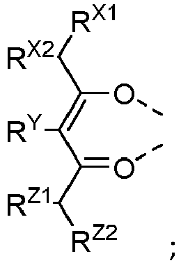 wobei RX1, RX2, RZ1, und RZ2 unabhängig ausgewählt sind aus der Gruppe bestehend aus Alkyl, Cycloalkyl, Aryl, und Heteroaryl; undwobei mindestens einer von RX1, RX2, RZ1, und RZ2 mindestens zwei Kohlenstoffatome aufweist.
 - Die Verbindung nach einem der Ansprüche 1 bis 7, wobei der Ligand LA ausgewählt ist aus der Gruppe bestehend aus:


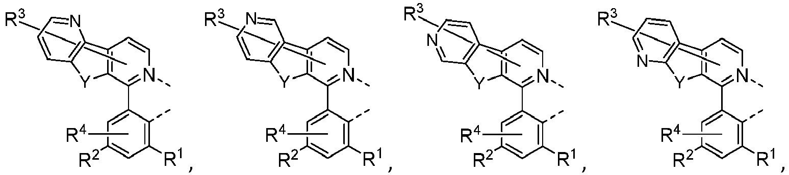


- Die Verbindung nach einem der Ansprüche 1 bis 8, wobei der Ligand LA ausgewählt ist aus der Gruppe bestehend aus:LA1 bis LA306 welche basiert sind auf einer Struktur gemäß Formel I,


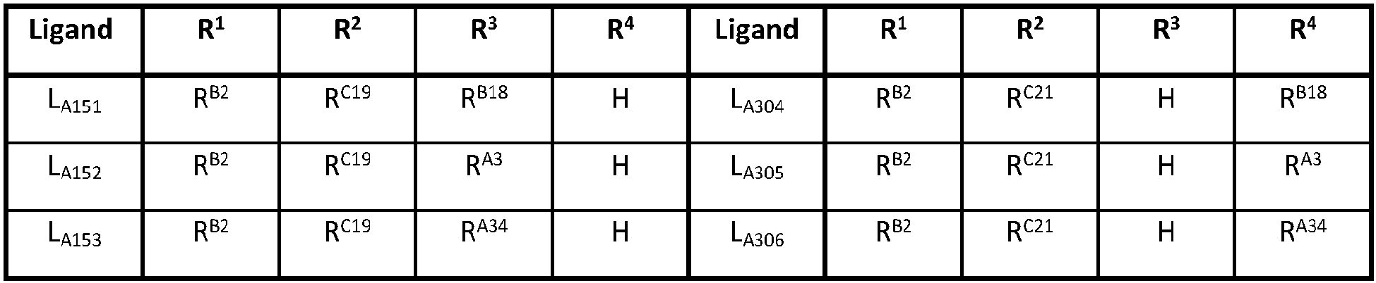 LA307 bis LA612, die basiert sind auf einer Struktur gemäß Formel II,


 LA613 bis LA9181 die basiert sind auf einer Struktur gemäß Formel III,


 LA919 bis LA1224, die basiert sind auf einer Struktur gemäß Formel IV,


 LA1225 bis LA1326, die basiert sind auf einer Struktur gemäß Formel V,


 LA1327 bis LA1428, die basiert sind auf einer Struktur gemäß Formel VI,
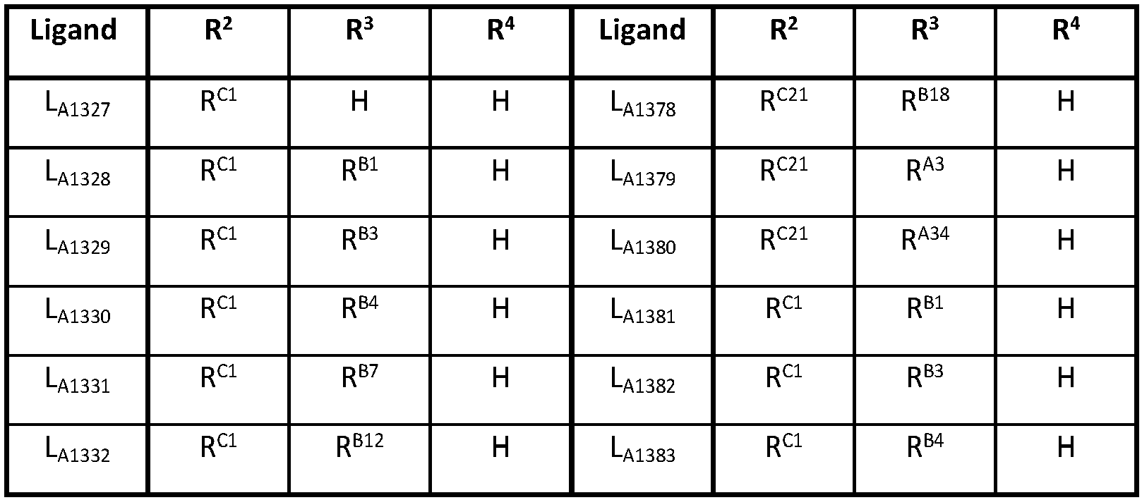

 LA1429 bis LA1530, die basiert sind auf einer Struktur gemäß Formel VII,

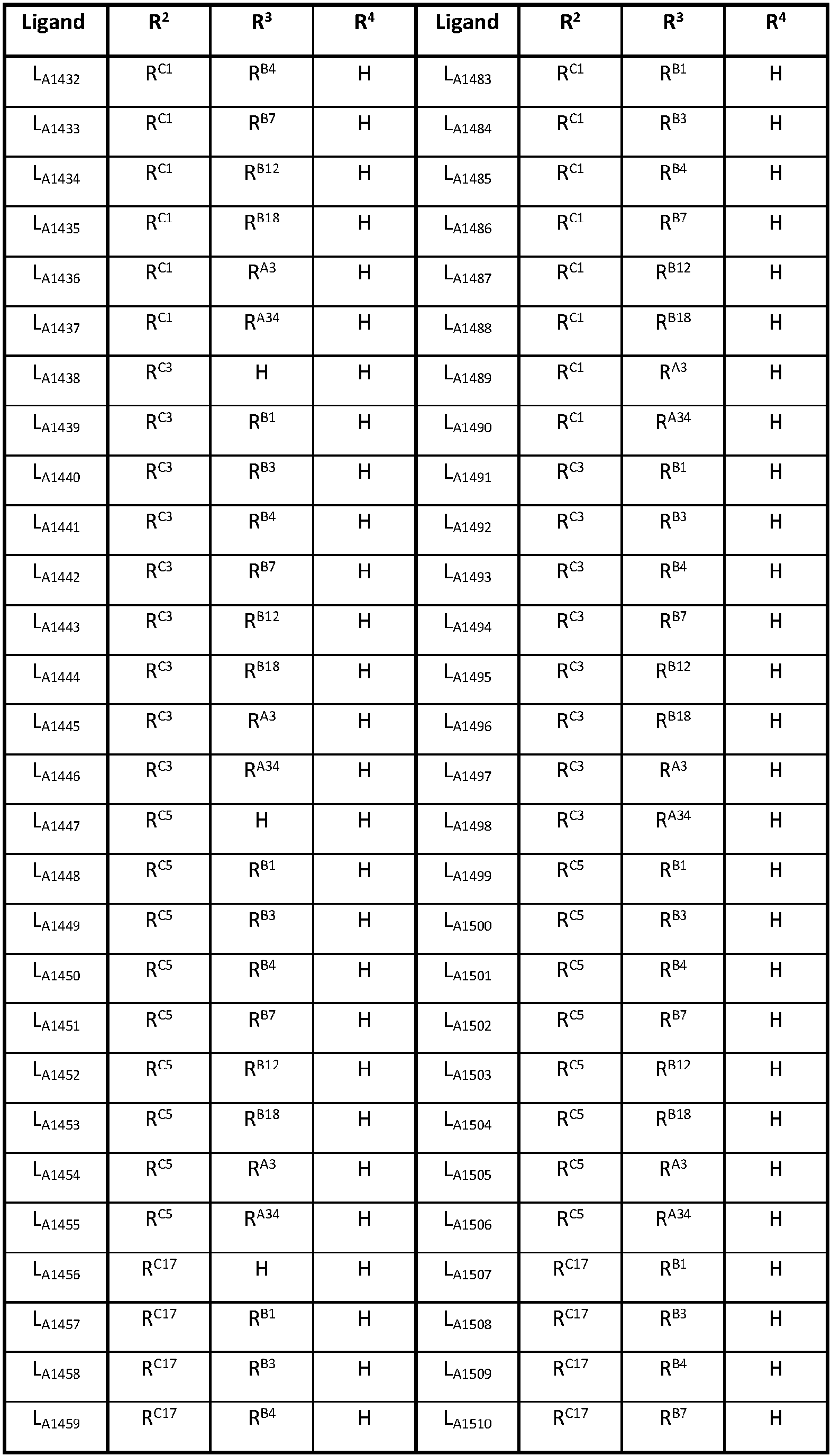
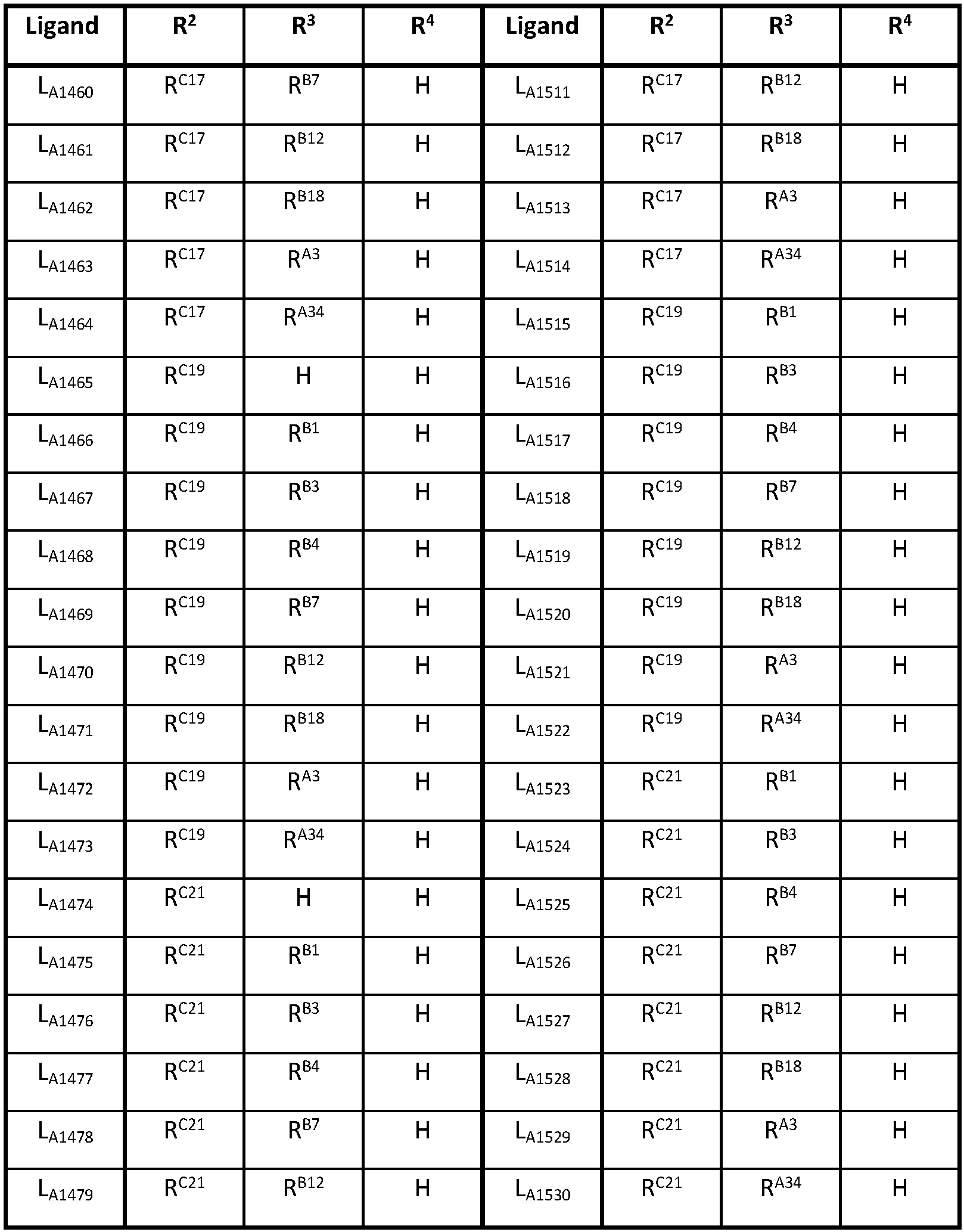 LA1531 bis LA1836, die basiert sind auf einer Struktur gemäß Formula VIII,


 LA1837 bis LA1938, die basiert sind auf einer Struktur gemäß Formel IX,


 LA1939 bis LA2778, die basiert sind auf einer Struktur gemäß Formel X,


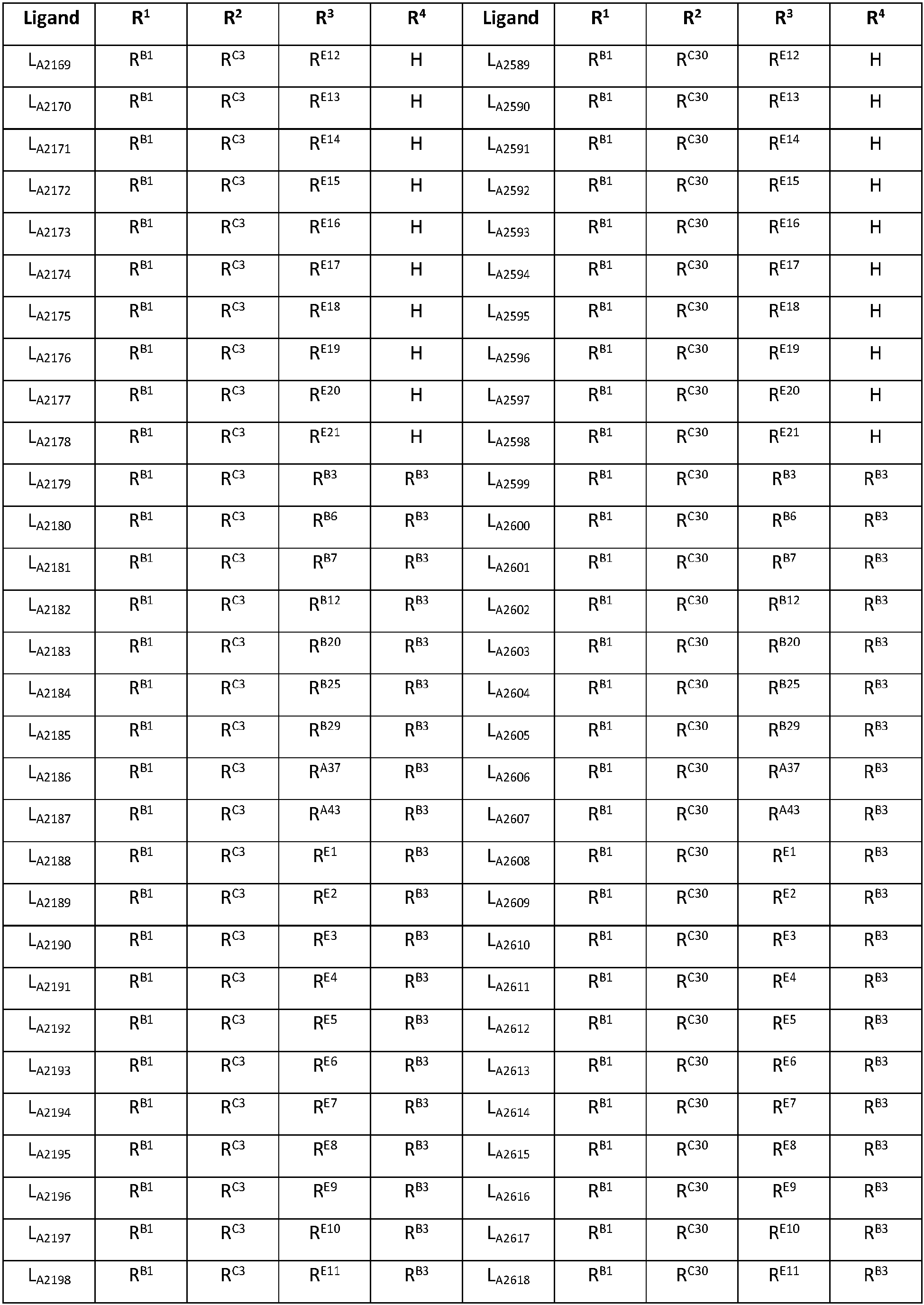


 LA2779 bis LA4038, die basiert sind auf einer Struktur gemäß Formel XI,
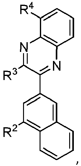


 LA4039 bis LA4878, die basiert sind auf einer Struktur gemäß Formel XII,


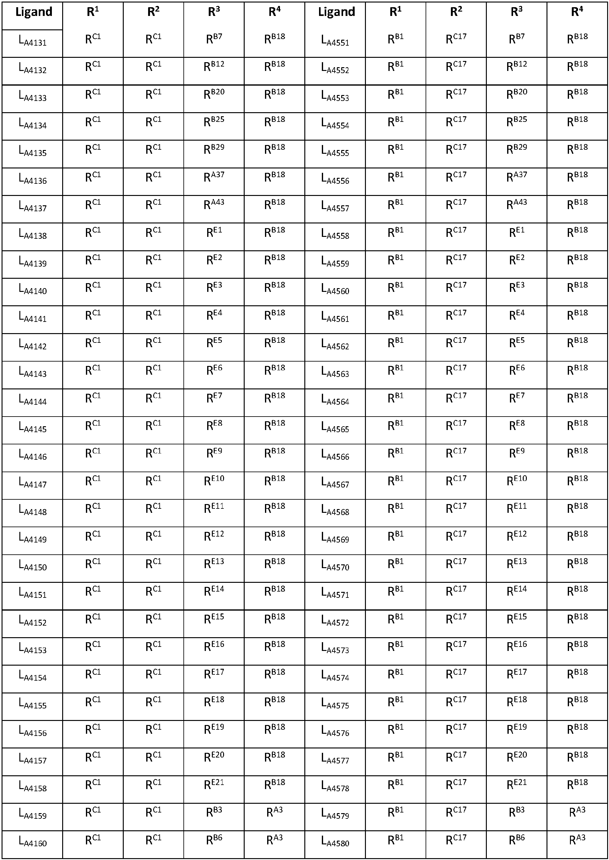


 LA4879 bis LA6138, welche basiert sind auf einer Struktur gemäß Formel XIII,


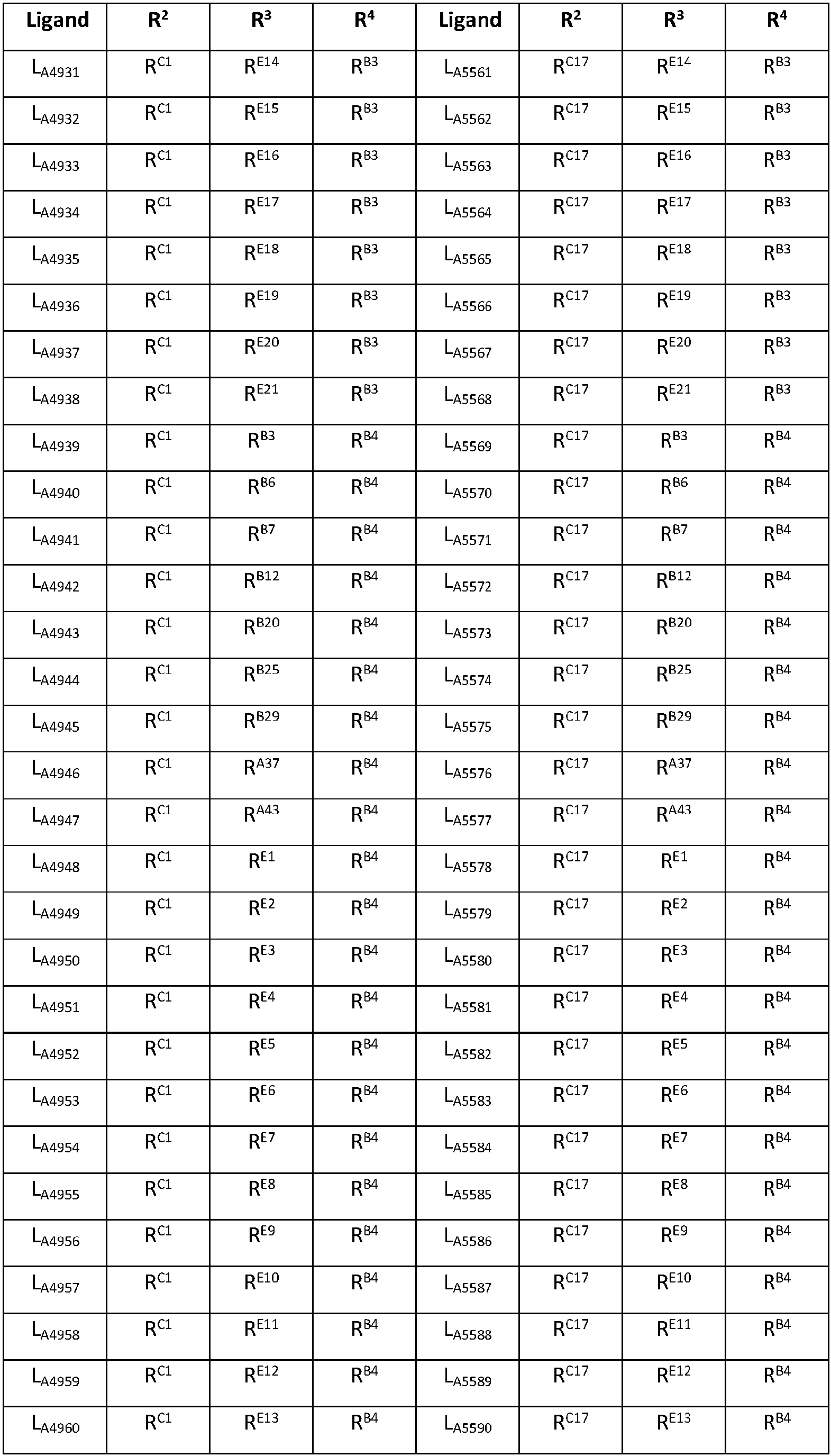


 wobei RB1 bis RB44 die folgenden Strukturen aufweisen:


 wobei RA1 bis RA52 die folgenden Strukturen aufweisen:
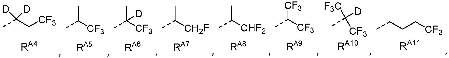


 wobei RE1 bis RE21 die folgenden Strukturen aufweisen:

 wobei LA6139 bis LA6154 die folgenden Strukturen aufweisen:


- Die Verbindung nach einem der Ansprüche 1 bis 9, wobei der Ligand LB ausgewählt ist aus der Gruppe bestehend aus:
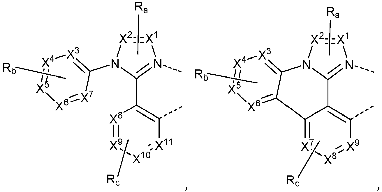

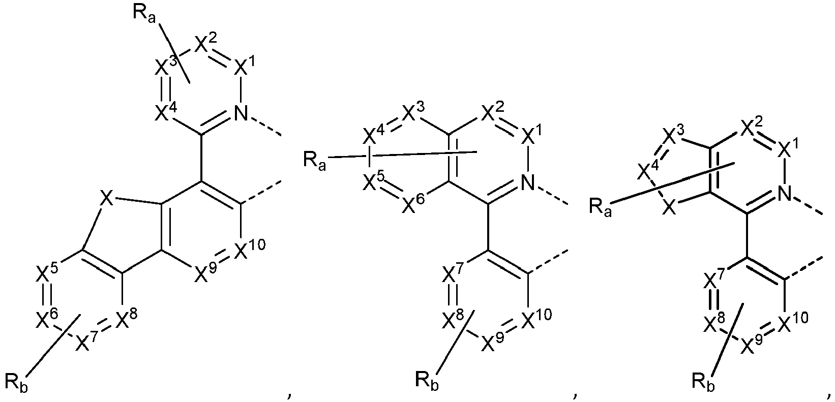


 wobei jedes X1 bis X13 unabhängig ausgewählt ist aus der Gruppe bestehend aus Kohlenstoff und Stickstoff;wobei X ausgewählt ist aus der Gruppe bestehend aus BR', NR', PR', O, S, Se, C=O, S=O, SO2, CR'R", SiR'R", und GeR'R";wobei R' und R" gegebenenfalls fusioniert oder verknüpft sind um einen Ring zu bilden;wobei jedes von Ra, Rb, Rc, und Rd für eine Monosubstitution bis zu einer maximalen Anzahl von Substitutionen oder keine Substitutionen steht;wobei R', R", Ra, Rb, Rc, und Rd jeweils unabhängig ausgewählt sind aus der Gruppe bestehend aus Wasserstoff, Deuterium, Alkyl, Cycloalkyl, Heteroalkyl, Alkoxy, Aryloxy, Amino, Silyl, Alkenyl, Cycloalkenyl, Heteroalkenyl, Aryl, Heteroaryl, Nitril, Isonitril, und deren Kombinationen; undwobei zwei beliebige benachbarte Substituenten von Ra, Rb, Rc, und Rd gegebenenfalls fusioniert oder verknüpft sind um einen Ring oder einen multidentaten Liganden zu bilden.
 - Die Verbindung nach einem der Ansprüche 1 bis 10, wobei der Ligand LC ausgewählt ist aus der Gruppe bestehend aus:LC1 bis LC1260, die basiert sind auf einer Struktur gemäß Formel XIV,

Ligand R1 R2 R3 Ligand R1 R2 R3 Ligand R1 R2 R3 LC1 RD1 RD1 H LC421 RD26 RD21 H LC841 RD7 RD14 RD1 LC2 RD2 RD2 H LC422 RD26 RD23 H LC842 RD7 RD15 RD1 LC3 RD3 RD3 H LC423 RD26 RD24 H LC843 RD7 RD16 RD1 LC4 RD4 RD4 H LC424 RD26 RD25 H LC844 RD7 RD17 RD1 LC5 RD5 RD5 H LC425 RD26 RD27 H LC845 RD7 RD18 RD1 LC6 RD6 RD6 H LC426 RD26 RD28 H LC846 RD7 RD19 RD1 LC7 RD7 RD7 H LC427 RD26 RD29 H LC847 RD7 RD20 RD1 LC8 RD8 RD8 H LC428 RD26 RD30 H LC848 RD7 RD21 RD1 LC9 RD9 RD9 H LC429 RD26 RD31 H LC849 RD7 RD22 RD1 LC10 RD10 RD10 H LC430 RD26 RD32 H LC850 RD7 RD23 RD1 LC11 RD11 RD11 H LC431 RD26 RD33 H LC851 RD7 RD24 RD1 LC12 RD12 RD12 H LC432 RD26 RD34 H LC852 RD7 RD25 RD1 LC13 RD13 RD13 H LC433 RD26 RD35 H LC853 RD7 RD26 RD1 LC14 RD14 RD14 H LC434 RD26 RD40 H LC854 RD7 RD27 RD1 LC15 RD15 RD15 H LC435 RD26 RD41 H LC855 RD7 RD28 RD1 LC16 RD16 RD16 H LC436 RD26 RD42 H LC856 RD7 RD29 RD1 LC17 RD17 RD17 H LC437 RD26 RD64 H LC857 RD7 RD30 RD1 LC18 RD18 RD18 H LC438 RD26 RD66 H LC858 RD7 RD31 RD1 


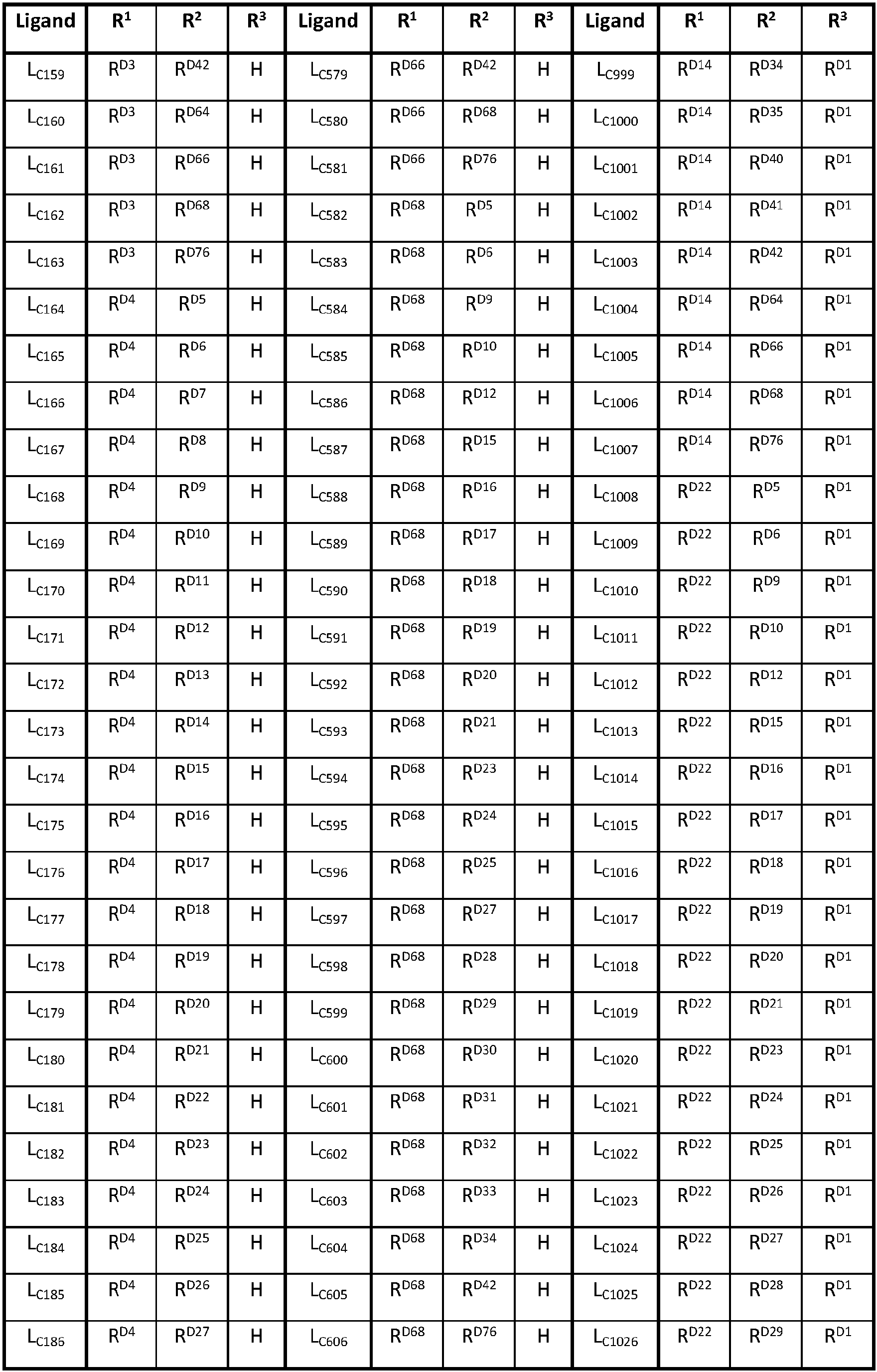

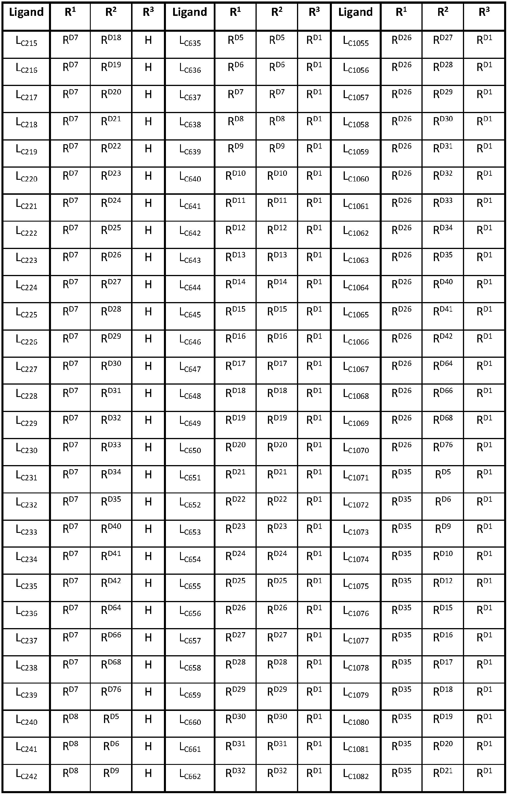


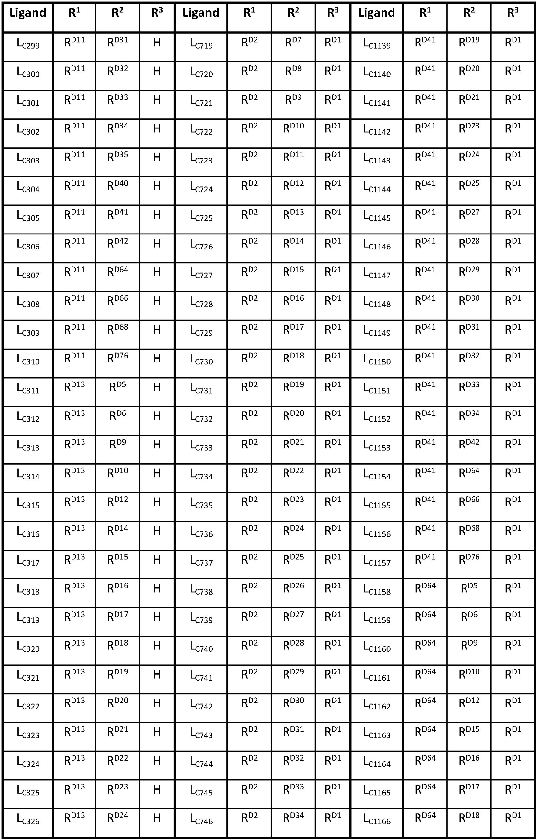

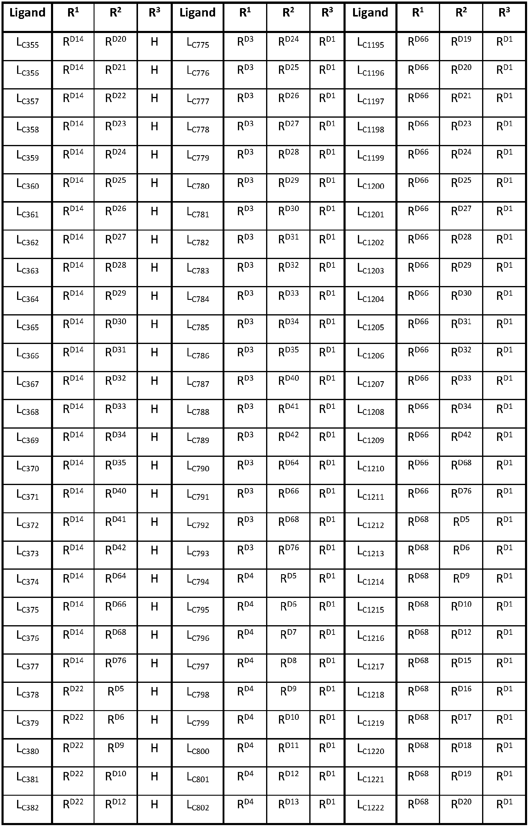

 wobei RD1 bis RD81 die folgenden Strukturen aufweisen:


- Die Verbindung nach Anspruch 9, wobei die Verbindung ausgewählt ist aus der Gruppe bestehend aus Verbindung x mit der Formel Ir(LAi )2(LCj ); wobei x eine ganze Zahl ist, die definiert wird durch x = 1260i+j-1260; wobei i eine ganze Zahl von 1 bis 6154 ist, und j eine ganze Zahl von 1 bis 1260 ist; wobei LC1 bis LC1260 die folgenden Strukturen aufweisen:LC1 bis LC1260 sind basiert auf einer Struktur gemäß Formel XV,
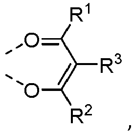
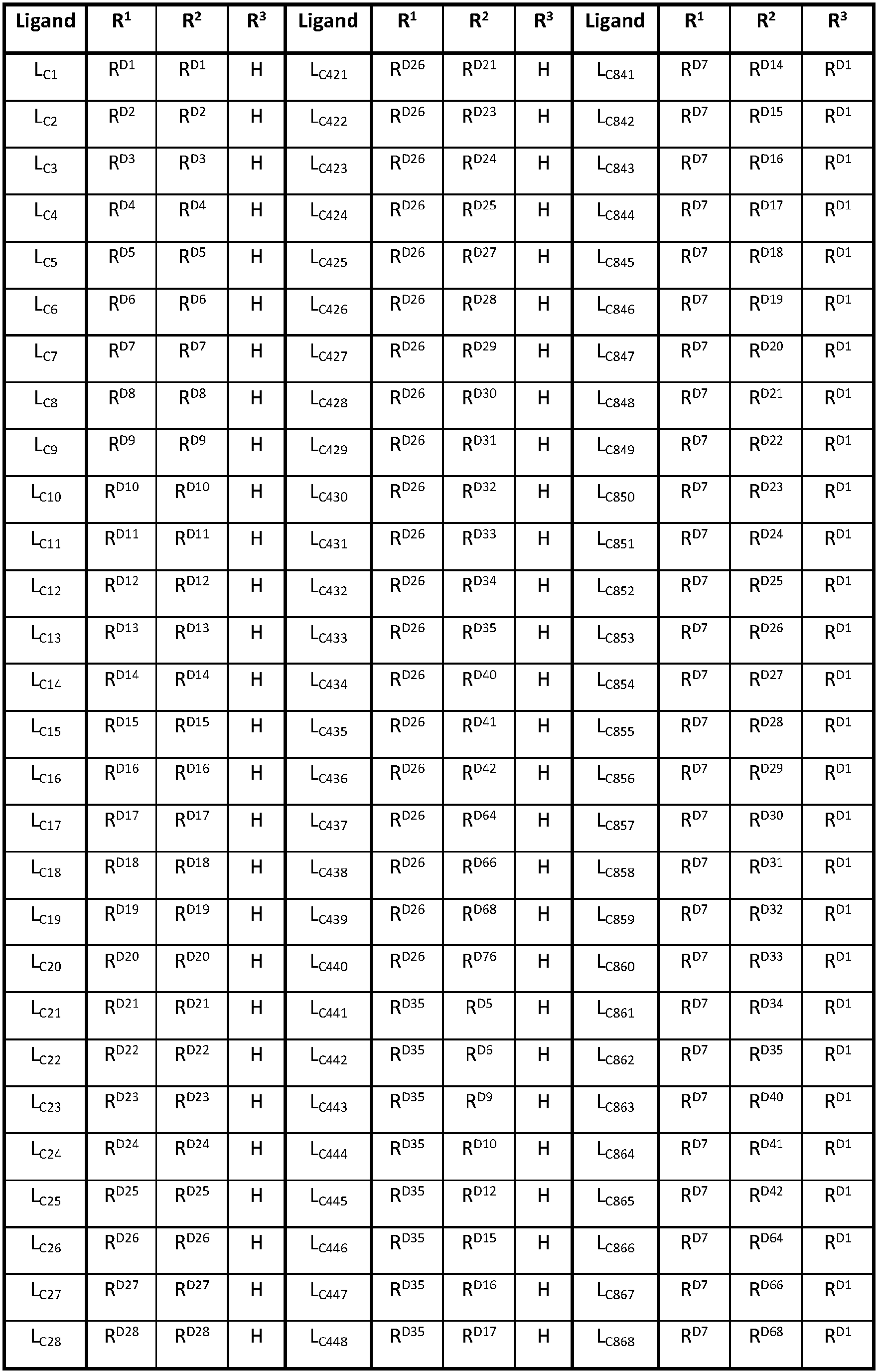


 wobei RD1 bis RD81 die folgenden Strukturen aufweisen:

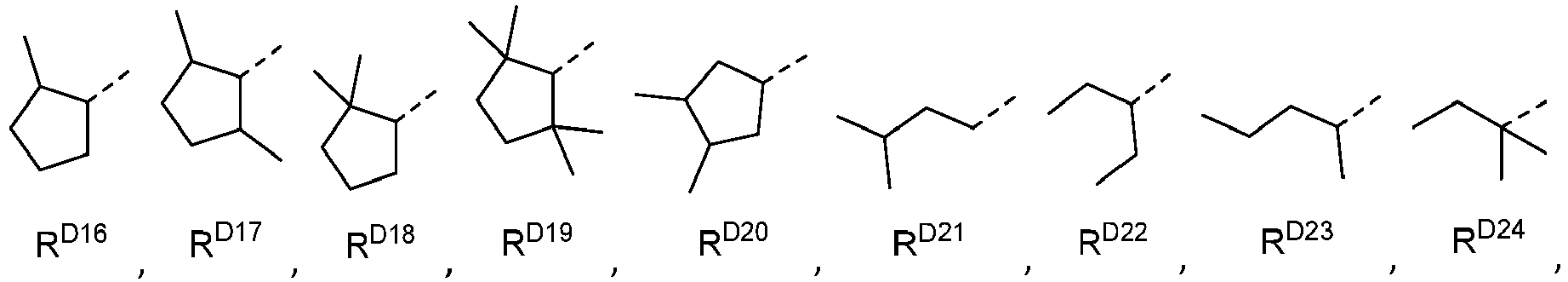


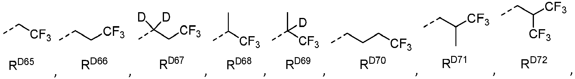


- Eine erste Vorrichtung umfassend eine erste organische Licht emittierende Vorrichtung (OLED), die erste OLED umfassend:eine Anode;eine Kathode; undeine organische Schicht, angeordnet zwischen der Anode und der Kathode, umfassend eine Verbindung wie in einem der Ansprüche 1 bis 12 definiert.
- Die erste Vorrichtung nach Anspruch 13, wobei die organische Schicht eine emittierende Schicht und die Verbindung ein emittierender Dotierstoff oder ein nicht emittierender Dotierstoff ist.
- Ein Konsumentenprodukt umfassend eine organische Licht emittierende Vorrichtung(OLED):eine Anode;eine Kathode; undeine organische Schicht, angeordnet zwischen der Anode und der Kathode, umfassend eine Verbindung wie in einem der Ansprüche 1 bis 12 definiert.
Applications Claiming Priority (2)
| Application Number | Priority Date | Filing Date | Title |
|---|---|---|---|
| US201762501906P | 2017-05-05 | 2017-05-05 | |
| US15/928,666 US10862055B2 (en) | 2017-05-05 | 2018-03-22 | Organic electroluminescent materials and devices |
Publications (2)
| Publication Number | Publication Date |
|---|---|
| EP3398953A1 EP3398953A1 (de) | 2018-11-07 |
| EP3398953B1 true EP3398953B1 (de) | 2020-09-09 |
Family
ID=62116275
Family Applications (1)
| Application Number | Title | Priority Date | Filing Date |
|---|---|---|---|
| EP18170637.5A Active EP3398953B1 (de) | 2017-05-05 | 2018-05-03 | Organische elektrolumineszente materialien und vorrichtungen |
Country Status (6)
| Country | Link |
|---|---|
| US (1) | US10862055B2 (de) |
| EP (1) | EP3398953B1 (de) |
| JP (1) | JP7022644B2 (de) |
| KR (1) | KR102637435B1 (de) |
| CN (1) | CN108794538A (de) |
| TW (1) | TWI755531B (de) |
Families Citing this family (8)
| Publication number | Priority date | Publication date | Assignee | Title |
|---|---|---|---|---|
| US11390639B2 (en) * | 2018-04-13 | 2022-07-19 | Universal Display Corporation | Organic electroluminescent materials and devices |
| US11459349B2 (en) | 2018-05-25 | 2022-10-04 | Universal Display Corporation | Organic electroluminescent materials and devices |
| KR20200120185A (ko) * | 2019-04-11 | 2020-10-21 | 삼성전자주식회사 | 유기금속 화합물, 이를 포함한 유기 발광 소자 및 이를 포함한 진단용 조성물 |
| CN112679548B (zh) | 2019-10-18 | 2023-07-28 | 北京夏禾科技有限公司 | 具有部分氟取代的取代基的辅助配体的有机发光材料 |
| KR20210086155A (ko) * | 2019-12-31 | 2021-07-08 | 엘지디스플레이 주식회사 | 발광 물질 및 그를 이용한 전계 발광 표시 장치 |
| CN113121609B (zh) * | 2020-01-16 | 2024-03-29 | 北京夏禾科技有限公司 | 一种金属配合物、包含其的电致发光器件及其用途 |
| US20220367820A1 (en) * | 2020-03-31 | 2022-11-17 | Universal Display Corporation | Organic electroluminescent materials and devices |
| EP3909964A3 (de) * | 2020-05-14 | 2022-02-16 | Samsung Electronics Co., Ltd. | Organometallische verbindung, organische lichtemittierende vorrichtung damit und elektronisches gerät mit der organischen lichtemittierenden vorrichtung |
Family Cites Families (151)
| Publication number | Priority date | Publication date | Assignee | Title |
|---|---|---|---|---|
| US4769292A (en) | 1987-03-02 | 1988-09-06 | Eastman Kodak Company | Electroluminescent device with modified thin film luminescent zone |
| GB8909011D0 (en) | 1989-04-20 | 1989-06-07 | Friend Richard H | Electroluminescent devices |
| US5061569A (en) | 1990-07-26 | 1991-10-29 | Eastman Kodak Company | Electroluminescent device with organic electroluminescent medium |
| DE69412567T2 (de) | 1993-11-01 | 1999-02-04 | Hodogaya Chemical Co Ltd | Aminverbindung und sie enthaltende Elektrolumineszenzvorrichtung |
| US5707745A (en) | 1994-12-13 | 1998-01-13 | The Trustees Of Princeton University | Multicolor organic light emitting devices |
| US5703436A (en) | 1994-12-13 | 1997-12-30 | The Trustees Of Princeton University | Transparent contacts for organic devices |
| US6939625B2 (en) | 1996-06-25 | 2005-09-06 | Nôrthwestern University | Organic light-emitting diodes and methods for assembly and enhanced charge injection |
| US5844363A (en) | 1997-01-23 | 1998-12-01 | The Trustees Of Princeton Univ. | Vacuum deposited, non-polymeric flexible organic light emitting devices |
| US6013982A (en) | 1996-12-23 | 2000-01-11 | The Trustees Of Princeton University | Multicolor display devices |
| US5834893A (en) | 1996-12-23 | 1998-11-10 | The Trustees Of Princeton University | High efficiency organic light emitting devices with light directing structures |
| US6091195A (en) | 1997-02-03 | 2000-07-18 | The Trustees Of Princeton University | Displays having mesa pixel configuration |
| US6303238B1 (en) | 1997-12-01 | 2001-10-16 | The Trustees Of Princeton University | OLEDs doped with phosphorescent compounds |
| US6337102B1 (en) | 1997-11-17 | 2002-01-08 | The Trustees Of Princeton University | Low pressure vapor phase deposition of organic thin films |
| US6087196A (en) | 1998-01-30 | 2000-07-11 | The Trustees Of Princeton University | Fabrication of organic semiconductor devices using ink jet printing |
| US6528187B1 (en) | 1998-09-08 | 2003-03-04 | Fuji Photo Film Co., Ltd. | Material for luminescence element and luminescence element using the same |
| US6097147A (en) | 1998-09-14 | 2000-08-01 | The Trustees Of Princeton University | Structure for high efficiency electroluminescent device |
| US6830828B2 (en) | 1998-09-14 | 2004-12-14 | The Trustees Of Princeton University | Organometallic complexes as phosphorescent emitters in organic LEDs |
| US6294398B1 (en) | 1999-11-23 | 2001-09-25 | The Trustees Of Princeton University | Method for patterning devices |
| US6458475B1 (en) | 1999-11-24 | 2002-10-01 | The Trustee Of Princeton University | Organic light emitting diode having a blue phosphorescent molecule as an emitter |
| KR100377321B1 (ko) | 1999-12-31 | 2003-03-26 | 주식회사 엘지화학 | 피-형 반도체 성질을 갖는 유기 화합물을 포함하는 전기소자 |
| US20020121638A1 (en) | 2000-06-30 | 2002-09-05 | Vladimir Grushin | Electroluminescent iridium compounds with fluorinated phenylpyridines, phenylpyrimidines, and phenylquinolines and devices made with such compounds |
| JP2002050860A (ja) | 2000-08-04 | 2002-02-15 | Toray Eng Co Ltd | 実装方法および実装装置 |
| US6579630B2 (en) | 2000-12-07 | 2003-06-17 | Canon Kabushiki Kaisha | Deuterated semiconducting organic compounds used for opto-electronic devices |
| JP3812730B2 (ja) | 2001-02-01 | 2006-08-23 | 富士写真フイルム株式会社 | 遷移金属錯体及び発光素子 |
| JP4307000B2 (ja) | 2001-03-08 | 2009-08-05 | キヤノン株式会社 | 金属配位化合物、電界発光素子及び表示装置 |
| JP4310077B2 (ja) | 2001-06-19 | 2009-08-05 | キヤノン株式会社 | 金属配位化合物及び有機発光素子 |
| ATE431970T1 (de) | 2001-06-20 | 2009-06-15 | Showa Denko Kk | Licht emittierendes material und organische leuchtdiode |
| US7071615B2 (en) | 2001-08-20 | 2006-07-04 | Universal Display Corporation | Transparent electrodes |
| US7250226B2 (en) | 2001-08-31 | 2007-07-31 | Nippon Hoso Kyokai | Phosphorescent compound, a phosphorescent composition and an organic light-emitting device |
| US7431968B1 (en) | 2001-09-04 | 2008-10-07 | The Trustees Of Princeton University | Process and apparatus for organic vapor jet deposition |
| US6835469B2 (en) | 2001-10-17 | 2004-12-28 | The University Of Southern California | Phosphorescent compounds and devices comprising the same |
| US7166368B2 (en) | 2001-11-07 | 2007-01-23 | E. I. Du Pont De Nemours And Company | Electroluminescent platinum compounds and devices made with such compounds |
| US6863997B2 (en) | 2001-12-28 | 2005-03-08 | The Trustees Of Princeton University | White light emitting OLEDs from combined monomer and aggregate emission |
| KR100691543B1 (ko) | 2002-01-18 | 2007-03-09 | 주식회사 엘지화학 | 새로운 전자 수송용 물질 및 이를 이용한 유기 발광 소자 |
| US20030230980A1 (en) | 2002-06-18 | 2003-12-18 | Forrest Stephen R | Very low voltage, high efficiency phosphorescent oled in a p-i-n structure |
| US7189989B2 (en) | 2002-08-22 | 2007-03-13 | Fuji Photo Film Co., Ltd. | Light emitting element |
| WO2004020549A1 (ja) | 2002-08-27 | 2004-03-11 | Fujitsu Limited | 有機金属錯体、有機el素子及び有機elディスプレイ |
| US6687266B1 (en) | 2002-11-08 | 2004-02-03 | Universal Display Corporation | Organic light emitting materials and devices |
| JP4365199B2 (ja) | 2002-12-27 | 2009-11-18 | 富士フイルム株式会社 | 有機電界発光素子 |
| JP4365196B2 (ja) | 2002-12-27 | 2009-11-18 | 富士フイルム株式会社 | 有機電界発光素子 |
| EP2062908B1 (de) | 2003-03-24 | 2016-07-13 | University of Southern California | Übergangsmetallkomplexe mit Pyrazolylcarbazol-Liganden |
| US7090928B2 (en) | 2003-04-01 | 2006-08-15 | The University Of Southern California | Binuclear compounds |
| WO2004093207A2 (de) | 2003-04-15 | 2004-10-28 | Covion Organic Semiconductors Gmbh | Mischungen von organischen zur emission befähigten halbleitern und matrixmaterialien, deren verwendung und elektronikbauteile enthaltend diese mischungen |
| US7029765B2 (en) | 2003-04-22 | 2006-04-18 | Universal Display Corporation | Organic light emitting devices having reduced pixel shrinkage |
| WO2004107822A1 (ja) | 2003-05-29 | 2004-12-09 | Nippon Steel Chemical Co., Ltd. | 有機電界発光素子 |
| JP2005011610A (ja) | 2003-06-18 | 2005-01-13 | Nippon Steel Chem Co Ltd | 有機電界発光素子 |
| US20050025993A1 (en) | 2003-07-25 | 2005-02-03 | Thompson Mark E. | Materials and structures for enhancing the performance of organic light emitting devices |
| TWI390006B (zh) | 2003-08-07 | 2013-03-21 | Nippon Steel Chemical Co | Organic EL materials with aluminum clamps |
| DE10338550A1 (de) | 2003-08-19 | 2005-03-31 | Basf Ag | Übergangsmetallkomplexe mit Carbenliganden als Emitter für organische Licht-emittierende Dioden (OLEDs) |
| US20060269780A1 (en) | 2003-09-25 | 2006-11-30 | Takayuki Fukumatsu | Organic electroluminescent device |
| JP4822687B2 (ja) | 2003-11-21 | 2011-11-24 | 富士フイルム株式会社 | 有機電界発光素子 |
| US7332232B2 (en) | 2004-02-03 | 2008-02-19 | Universal Display Corporation | OLEDs utilizing multidentate ligand systems |
| EP1725079B1 (de) | 2004-03-11 | 2013-05-08 | Mitsubishi Chemical Corporation | Zusammensetzung für ladungstransportierenden film und ionenverbindung, ladungstransportierender film und diesen verwendende organische elektrolumineszenzvorrichtung, und verfahren zur herstellung einer organischen elektrolumineszenzvorrichtung und verfahren zur herstellung eines ladungstransportierenden films |
| TW200531592A (en) | 2004-03-15 | 2005-09-16 | Nippon Steel Chemical Co | Organic electroluminescent device |
| JP4869565B2 (ja) | 2004-04-23 | 2012-02-08 | 富士フイルム株式会社 | 有機電界発光素子 |
| US7154114B2 (en) | 2004-05-18 | 2006-12-26 | Universal Display Corporation | Cyclometallated iridium carbene complexes for use as hosts |
| US7279704B2 (en) | 2004-05-18 | 2007-10-09 | The University Of Southern California | Complexes with tridentate ligands |
| US7491823B2 (en) | 2004-05-18 | 2009-02-17 | The University Of Southern California | Luminescent compounds with carbene ligands |
| US7534505B2 (en) | 2004-05-18 | 2009-05-19 | The University Of Southern California | Organometallic compounds for use in electroluminescent devices |
| US7393599B2 (en) | 2004-05-18 | 2008-07-01 | The University Of Southern California | Luminescent compounds with carbene ligands |
| US7445855B2 (en) | 2004-05-18 | 2008-11-04 | The University Of Southern California | Cationic metal-carbene complexes |
| WO2005123873A1 (ja) | 2004-06-17 | 2005-12-29 | Konica Minolta Holdings, Inc. | 有機エレクトロルミネッセンス素子材料、有機エレクトロルミネッセンス素子、表示装置及び照明装置 |
| KR101272490B1 (ko) | 2004-06-28 | 2013-06-07 | 시바 홀딩 인크 | 트리아졸 및 벤조트리아졸을 갖는 전계발광 금속 착물 |
| US20060008670A1 (en) | 2004-07-06 | 2006-01-12 | Chun Lin | Organic light emitting materials and devices |
| EP2271183B1 (de) | 2004-07-23 | 2015-03-18 | Konica Minolta Holdings, Inc. | Organisches Elektrolumineszenzbauelement, Bildschirm und Beleuchtungseinheit |
| DE102004057072A1 (de) | 2004-11-25 | 2006-06-01 | Basf Ag | Verwendung von Übergangsmetall-Carbenkomplexen in organischen Licht-emittierenden Dioden (OLEDs) |
| WO2006072002A2 (en) | 2004-12-30 | 2006-07-06 | E.I. Dupont De Nemours And Company | Organometallic complexes |
| JPWO2006082742A1 (ja) | 2005-02-04 | 2008-06-26 | コニカミノルタホールディングス株式会社 | 有機エレクトロルミネッセンス素子材料、有機エレクトロルミネッセンス素子、表示装置及び照明装置 |
| KR100803125B1 (ko) | 2005-03-08 | 2008-02-14 | 엘지전자 주식회사 | 적색 인광 화합물 및 이를 사용한 유기전계발광소자 |
| WO2006098120A1 (ja) | 2005-03-16 | 2006-09-21 | Konica Minolta Holdings, Inc. | 有機エレクトロルミネッセンス素子材料、有機エレクトロルミネッセンス素子 |
| DE102005014284A1 (de) | 2005-03-24 | 2006-09-28 | Basf Ag | Verwendung von Verbindungen, welche aromatische oder heteroaromatische über Carbonyl-Gruppen enthaltende Gruppen verbundene Ringe enthalten, als Matrixmaterialien in organischen Leuchtdioden |
| WO2006103874A1 (ja) | 2005-03-29 | 2006-10-05 | Konica Minolta Holdings, Inc. | 有機エレクトロルミネッセンス素子材料、有機エレクトロルミネッセンス素子、表示装置及び照明装置 |
| WO2006114966A1 (ja) | 2005-04-18 | 2006-11-02 | Konica Minolta Holdings, Inc. | 有機エレクトロルミネッセンス素子、表示装置及び照明装置 |
| US7807275B2 (en) | 2005-04-21 | 2010-10-05 | Universal Display Corporation | Non-blocked phosphorescent OLEDs |
| JP4533796B2 (ja) | 2005-05-06 | 2010-09-01 | 富士フイルム株式会社 | 有機電界発光素子 |
| US9051344B2 (en) | 2005-05-06 | 2015-06-09 | Universal Display Corporation | Stability OLED materials and devices |
| CN103746080B (zh) | 2005-05-31 | 2019-03-08 | 通用显示公司 | 发射磷光的二极管中的苯并[9,10]菲基质 |
| JP4976288B2 (ja) | 2005-06-07 | 2012-07-18 | 新日鐵化学株式会社 | 有機金属錯体及びこれを用いた有機電界発光素子 |
| KR101294905B1 (ko) | 2005-06-27 | 2013-08-09 | 이 아이 듀폰 디 네모아 앤드 캄파니 | 전기 전도성 중합체 조성물 |
| US20090039771A1 (en) | 2005-07-01 | 2009-02-12 | Konica Minolta Holdings, Inc. | Organic electroluminescent element material, organic electroluminescent element, display device and lighting device |
| WO2007028417A1 (en) | 2005-09-07 | 2007-03-15 | Technische Universität Braunschweig | Triplett emitter having condensed five-membered rings |
| JP4887731B2 (ja) | 2005-10-26 | 2012-02-29 | コニカミノルタホールディングス株式会社 | 有機エレクトロルミネッセンス素子、表示装置及び照明装置 |
| JPWO2007063796A1 (ja) | 2005-12-01 | 2009-05-07 | 新日鐵化学株式会社 | 有機電界発光素子 |
| CN101321755B (zh) | 2005-12-01 | 2012-04-18 | 新日铁化学株式会社 | 有机电致发光元件用化合物及有机电致发光元件 |
| CN101415718B (zh) | 2006-02-10 | 2013-05-29 | 通用显示公司 | 环金属化的咪唑并[1,2-f]菲啶和二咪唑并[1,2-a:1',2'-c]喹唑啉配位体和其等电子和苯并环化类似物的金属络合物 |
| JP4823730B2 (ja) | 2006-03-20 | 2011-11-24 | 新日鐵化学株式会社 | 発光層化合物及び有機電界発光素子 |
| WO2007125714A1 (ja) | 2006-04-26 | 2007-11-08 | Idemitsu Kosan Co., Ltd. | 芳香族アミン誘導体及びそれらを用いた有機エレクトロルミネッセンス素子 |
| KR101384046B1 (ko) | 2006-05-11 | 2014-04-09 | 이데미쓰 고산 가부시키가이샤 | 유기 전계발광 소자 |
| KR20090016684A (ko) | 2006-06-02 | 2009-02-17 | 이데미쓰 고산 가부시키가이샤 | 유기 전기발광 소자용 재료 및 그것을 이용한 유기 전기발광 소자 |
| KR20090040896A (ko) | 2006-08-23 | 2009-04-27 | 이데미쓰 고산 가부시키가이샤 | 방향족 아민 유도체 및 이들을 이용한 유기 전기발광 소자 |
| JP4251206B2 (ja) * | 2006-09-20 | 2009-04-08 | セイコーエプソン株式会社 | アクチュエータ、光スキャナおよび画像形成装置 |
| JP5589251B2 (ja) | 2006-09-21 | 2014-09-17 | コニカミノルタ株式会社 | 有機エレクトロルミネッセンス素子材料 |
| CN101511834B (zh) | 2006-11-09 | 2013-03-27 | 新日铁化学株式会社 | 有机场致发光元件用化合物及有机场致发光元件 |
| JP5133259B2 (ja) | 2006-11-24 | 2013-01-30 | 出光興産株式会社 | 芳香族アミン誘導体及びそれを用いた有機エレクトロルミネッセンス素子 |
| US8119255B2 (en) | 2006-12-08 | 2012-02-21 | Universal Display Corporation | Cross-linkable iridium complexes and organic light-emitting devices using the same |
| US8778508B2 (en) | 2006-12-08 | 2014-07-15 | Universal Display Corporation | Light-emitting organometallic complexes |
| EP2112994B1 (de) | 2007-02-23 | 2011-01-26 | Basf Se | Elektrolumineszente metallkomplexe mit benzotriazolen |
| DE502008002309D1 (de) | 2007-04-26 | 2011-02-24 | Basf Se | Silane enthaltend phenothiazin-s-oxid oder phenothiazin-s,s-dioxid-gruppen und deren verwendung in oleds |
| WO2008156879A1 (en) | 2007-06-20 | 2008-12-24 | Universal Display Corporation | Blue phosphorescent imidazophenanthridine materials |
| KR101539789B1 (ko) | 2007-06-22 | 2015-07-27 | 바스프 에스이 | 발광 cu(i) 착물 |
| EP2165377B1 (de) | 2007-07-05 | 2021-04-28 | UDC Ireland Limited | Organische leuchtdioden enthaltend carben-übergangsmetall-komplex-emitter und mindestens eine verbindung ausgewählt aus disilylcarbazolen; disilyldibenzofuranen, disilyldibenzothiophenen, disilyldibenzophospholen, disilyldibenzothiophen-s-oxiden und disilyldibenzothiophen-s,s-dioxiden |
| US8029697B2 (en) | 2007-07-07 | 2011-10-04 | Idemitsu Kosan Co., Ltd. | Naphthalene derivative, material for organic electroluminescence device, and organic electroluminescence device using the same |
| US20090045731A1 (en) | 2007-07-07 | 2009-02-19 | Idemitsu Kosan Co., Ltd. | Organic electroluminescence device and material for organic electroluminescence device |
| US8221907B2 (en) | 2007-07-07 | 2012-07-17 | Idemitsu Kosan Co., Ltd. | Chrysene derivative and organic electroluminescent device using the same |
| WO2009008205A1 (ja) | 2007-07-07 | 2009-01-15 | Idemitsu Kosan Co., Ltd. | 有機エレクトロルミネッセンス素子および有機エレクトロルミネッセンス素子用材料 |
| US8779655B2 (en) | 2007-07-07 | 2014-07-15 | Idemitsu Kosan Co., Ltd. | Organic electroluminescence device and material for organic electroluminescence device |
| US7968213B2 (en) | 2007-07-10 | 2011-06-28 | Idemitsu Kosan Co., Ltd. | Material for organic electroluminescence device and organic electroluminescence device utilizing the same |
| US8080658B2 (en) | 2007-07-10 | 2011-12-20 | Idemitsu Kosan Co., Ltd. | Material for organic electroluminescent element and organic electroluminescent element employing the same |
| CN101688052A (zh) | 2007-07-27 | 2010-03-31 | E.I.内穆尔杜邦公司 | 包含无机纳米颗粒的导电聚合物的含水分散体 |
| KR101787850B1 (ko) | 2007-08-08 | 2017-10-18 | 유니버셜 디스플레이 코포레이션 | 트리페닐렌기를 포함하는 벤조 융합 티오펜 또는 벤조 융합 푸란 화합물 |
| JP2009040728A (ja) | 2007-08-09 | 2009-02-26 | Canon Inc | 有機金属錯体及びこれを用いた有機発光素子 |
| EP2203461B1 (de) | 2007-10-17 | 2011-08-10 | Basf Se | Übergangsmetallkomplexe mit verbrückten carbenliganden und deren verwendung in oleds |
| KR100950968B1 (ko) | 2007-10-18 | 2010-04-02 | 에스에프씨 주식회사 | 적색 인광 화합물 및 이를 이용한 유기전계발광소자 |
| US20090101870A1 (en) | 2007-10-22 | 2009-04-23 | E. I. Du Pont De Nemours And Company | Electron transport bi-layers and devices made with such bi-layers |
| US7914908B2 (en) | 2007-11-02 | 2011-03-29 | Global Oled Technology Llc | Organic electroluminescent device having an azatriphenylene derivative |
| DE102007053771A1 (de) | 2007-11-12 | 2009-05-14 | Merck Patent Gmbh | Organische Elektrolumineszenzvorrichtungen |
| KR101353635B1 (ko) | 2007-11-15 | 2014-01-20 | 이데미쓰 고산 가부시키가이샤 | 벤조크리센 유도체 및 이것을 사용한 유기 전계 발광 소자 |
| WO2009066779A1 (ja) | 2007-11-22 | 2009-05-28 | Idemitsu Kosan Co., Ltd. | 有機el素子 |
| EP2221897A4 (de) | 2007-11-22 | 2012-08-08 | Idemitsu Kosan Co | Organisches el-element und ein organisches el-material enthaltende lösung |
| WO2009085344A2 (en) | 2007-12-28 | 2009-07-09 | Universal Display Corporation | Dibenzothiophene-containing materials in phosphorescent light emitting diodes |
| US8221905B2 (en) | 2007-12-28 | 2012-07-17 | Universal Display Corporation | Carbazole-containing materials in phosphorescent light emitting diodes |
| WO2009100991A1 (en) | 2008-02-12 | 2009-08-20 | Basf Se | Electroluminescent metal complexes with dibenzo[f,h]quinoxalines |
| WO2010031738A1 (en) | 2008-09-22 | 2010-03-25 | Basf Se | Electroluminescent metal complexes with azapyrenes |
| JP5554075B2 (ja) * | 2009-01-21 | 2014-07-23 | 株式会社半導体エネルギー研究所 | 有機金属錯体 |
| KR101726459B1 (ko) | 2009-04-06 | 2017-04-12 | 유니버셜 디스플레이 코포레이션 | 신규한 리간드 구조를 포함하는 금속 착체 |
| JP4474493B1 (ja) * | 2009-07-31 | 2010-06-02 | 富士フイルム株式会社 | 有機電界発光素子 |
| GB201004151D0 (en) | 2010-03-13 | 2010-04-28 | Univ York | Luminophores |
| US8269317B2 (en) * | 2010-11-11 | 2012-09-18 | Universal Display Corporation | Phosphorescent materials |
| JP5901272B2 (ja) | 2010-12-24 | 2016-04-06 | 株式会社半導体エネルギー研究所 | 有機金属錯体、発光素子、発光装置、電子機器及び照明装置 |
| EP2883880B1 (de) * | 2012-08-08 | 2016-11-30 | Mitsubishi Chemical Corporation | Iridiumkomplexverbindung und zusammensetzung, organisches elektrolumineszenzelement, anzeigevorrichtung und beleuchtungsvorrichtung mit jeweils der verbindung |
| CN103965255A (zh) | 2013-01-31 | 2014-08-06 | 海洋王照明科技股份有限公司 | 一种红光有机电致磷光材料金属铱配合物及其制备方法和有机电致发光器件 |
| CN103965261A (zh) | 2013-01-31 | 2014-08-06 | 海洋王照明科技股份有限公司 | 红光有机电致磷光材料金属铱配合物及其制备方法和有机电致发光器件 |
| CN104140440A (zh) | 2013-05-09 | 2014-11-12 | 海洋王照明科技股份有限公司 | 一种红光有机电致磷光材料铱金属配合物及其制备方法和有机电致发光器件 |
| CN104140446A (zh) | 2013-05-09 | 2014-11-12 | 海洋王照明科技股份有限公司 | 一种红光有机电致磷光材料铱金属配合物及其制备方法和有机电致发光器件 |
| CN104140447A (zh) | 2013-05-09 | 2014-11-12 | 海洋王照明科技股份有限公司 | 一种红光有机电致磷光材料铱金属配合物及其制备方法和有机电致发光器件 |
| CN104140441A (zh) | 2013-05-09 | 2014-11-12 | 海洋王照明科技股份有限公司 | 一种红光有机电致磷光材料铱金属配合物及其制备方法和有机电致发光器件 |
| TW201444949A (zh) * | 2013-05-21 | 2014-12-01 | Nat Univ Tsing Hua | 銥金屬錯合物光電材料及其有機發光二極體 |
| CN105283461B (zh) * | 2013-06-14 | 2018-07-17 | 株式会社半导体能源研究所 | 有机金属铱配合物、发光元件、发光装置以及照明装置 |
| CN105814069A (zh) * | 2013-12-12 | 2016-07-27 | 三菱化学株式会社 | 铱配位化合物及其制造方法、含有其的组合物、有机场致发光元件、显示装置和照明装置 |
| CN103936791B (zh) | 2013-12-12 | 2016-10-12 | 石家庄诚志永华显示材料有限公司 | 一系列有机电致磷光材料 |
| US9590194B2 (en) | 2014-02-14 | 2017-03-07 | Universal Display Corporation | Organic electroluminescent materials and devices |
| US10003033B2 (en) * | 2014-02-18 | 2018-06-19 | Universal Display Corporation | Organic electroluminescent materials and devices |
| US9929353B2 (en) * | 2014-04-02 | 2018-03-27 | Universal Display Corporation | Organic electroluminescent materials and devices |
| US10457699B2 (en) * | 2014-05-02 | 2019-10-29 | Universal Display Corporation | Organic electroluminescent materials and devices |
| KR102388398B1 (ko) * | 2014-05-08 | 2022-04-20 | 유니버셜 디스플레이 코포레이션 | 안정화된 이미다조페난트리딘 물질 |
| CN104193783B (zh) | 2014-07-31 | 2017-05-17 | 石家庄诚志永华显示材料有限公司 | 苯并异喹啉金属配合物及其制备方法与应用 |
| US9397302B2 (en) | 2014-10-08 | 2016-07-19 | Universal Display Corporation | Organic electroluminescent materials and devices |
| JP6697299B2 (ja) | 2015-04-01 | 2020-05-20 | 株式会社半導体エネルギー研究所 | 有機金属錯体、発光素子、発光装置、電子機器、および照明装置 |
| JP6631034B2 (ja) | 2015-05-08 | 2020-01-15 | コニカミノルタ株式会社 | 有機エレクトロルミネッセンス素子用材料、有機エレクトロルミネッセンス素子、及び有機金属錯体 |
| US9859510B2 (en) * | 2015-05-15 | 2018-01-02 | Universal Display Corporation | Organic electroluminescent materials and devices |
| CN105505378B (zh) | 2015-12-21 | 2018-11-20 | 中国科学院长春应用化学研究所 | 以呋喃[3,2-c]吡啶单元金属配合物作为发光层的有机电致发光器件 |
-
2018
- 2018-03-22 US US15/928,666 patent/US10862055B2/en active Active
- 2018-04-17 JP JP2018078838A patent/JP7022644B2/ja active Active
- 2018-04-30 KR KR1020180049739A patent/KR102637435B1/ko active IP Right Grant
- 2018-05-03 EP EP18170637.5A patent/EP3398953B1/de active Active
- 2018-05-04 TW TW107115330A patent/TWI755531B/zh active
- 2018-05-07 CN CN201810428086.6A patent/CN108794538A/zh active Pending
Non-Patent Citations (1)
| Title |
|---|
| None * |
Also Published As
| Publication number | Publication date |
|---|---|
| JP2018188422A (ja) | 2018-11-29 |
| KR20180122946A (ko) | 2018-11-14 |
| JP7022644B2 (ja) | 2022-02-18 |
| US10862055B2 (en) | 2020-12-08 |
| EP3398953A1 (de) | 2018-11-07 |
| US20180323382A1 (en) | 2018-11-08 |
| TWI755531B (zh) | 2022-02-21 |
| CN108794538A (zh) | 2018-11-13 |
| TW201843295A (zh) | 2018-12-16 |
| KR102637435B1 (ko) | 2024-02-15 |
Similar Documents
| Publication | Publication Date | Title |
|---|---|---|
| KR102531522B1 (ko) | 유기 전계발광 물질 및 디바이스 | |
| EP3098229B1 (de) | Organische elektrolumineszente materialien und vorrichtungen | |
| KR102562931B1 (ko) | 유기 전계발광 재료 및 디바이스 | |
| EP3270435B1 (de) | Organische elektrolumineszente materialien und vorrichtungen | |
| EP3261146B1 (de) | Organische elektrolumineszente materialien und vorrichtungen | |
| EP3398953B1 (de) | Organische elektrolumineszente materialien und vorrichtungen | |
| EP3424934B1 (de) | Organische elektrolumineszente materialien und vorrichtungen | |
| JP7482939B2 (ja) | 有機エレクトロルミネセンス材料及びデバイス | |
| EP3297051B1 (de) | Organische elektrolumineszente materialien und vorrichtungen | |
| KR20160056844A (ko) | 유기 전계발광 물질 및 디바이스 | |
| KR20150126308A (ko) | 유기 전계발광 재료 및 소자 | |
| EP2542644A1 (de) | Phosphoreszierende materialien | |
| EP3231809A2 (de) | Organische elektrolumineszente materialien und vorrichtungen | |
| KR102461292B1 (ko) | 유기 전계발광 물질 및 디바이스 | |
| KR20170133281A (ko) | 유기 전계발광 물질 및 디바이스 | |
| EP3305796B1 (de) | Organische elektrolumineszente materialien und vorrichtungen | |
| KR102419312B1 (ko) | 유기 전계발광 재료 및 소자 | |
| KR102557211B1 (ko) | 유기 전계발광 물질 및 디바이스 | |
| EP3323822B1 (de) | Organische elektrolumineszente materialien und vorrichtungen | |
| KR20230112098A (ko) | 유기 전계발광 물질 및 디바이스 | |
| KR20230145289A (ko) | 유기 전계발광 물질 및 디바이스 | |
| KR20230022934A (ko) | 유기 전계발광 재료 및 디바이스 | |
| KR20230136585A (ko) | 전계발광 디바이스용 유기 호스트 물질 | |
| EP3354654B1 (de) | Organische elektrolumineszente materialien und vorrichtungen | |
| CN112794814A (zh) | 有机电致发光材料和装置 |
Legal Events
| Date | Code | Title | Description |
|---|---|---|---|
| PUAI | Public reference made under article 153(3) epc to a published international application that has entered the european phase |
Free format text: ORIGINAL CODE: 0009012 |
|
| STAA | Information on the status of an ep patent application or granted ep patent |
Free format text: STATUS: THE APPLICATION HAS BEEN PUBLISHED |
|
| AK | Designated contracting states |
Kind code of ref document: A1 Designated state(s): AL AT BE BG CH CY CZ DE DK EE ES FI FR GB GR HR HU IE IS IT LI LT LU LV MC MK MT NL NO PL PT RO RS SE SI SK SM TR |
|
| AX | Request for extension of the european patent |
Extension state: BA ME |
|
| STAA | Information on the status of an ep patent application or granted ep patent |
Free format text: STATUS: REQUEST FOR EXAMINATION WAS MADE |
|
| 17P | Request for examination filed |
Effective date: 20190415 |
|
| RBV | Designated contracting states (corrected) |
Designated state(s): AL AT BE BG CH CY CZ DE DK EE ES FI FR GB GR HR HU IE IS IT LI LT LU LV MC MK MT NL NO PL PT RO RS SE SI SK SM TR |
|
| STAA | Information on the status of an ep patent application or granted ep patent |
Free format text: STATUS: EXAMINATION IS IN PROGRESS |
|
| 17Q | First examination report despatched |
Effective date: 20190909 |
|
| GRAP | Despatch of communication of intention to grant a patent |
Free format text: ORIGINAL CODE: EPIDOSNIGR1 |
|
| STAA | Information on the status of an ep patent application or granted ep patent |
Free format text: STATUS: GRANT OF PATENT IS INTENDED |
|
| INTG | Intention to grant announced |
Effective date: 20200406 |
|
| GRAS | Grant fee paid |
Free format text: ORIGINAL CODE: EPIDOSNIGR3 |
|
| GRAA | (expected) grant |
Free format text: ORIGINAL CODE: 0009210 |
|
| STAA | Information on the status of an ep patent application or granted ep patent |
Free format text: STATUS: THE PATENT HAS BEEN GRANTED |
|
| AK | Designated contracting states |
Kind code of ref document: B1 Designated state(s): AL AT BE BG CH CY CZ DE DK EE ES FI FR GB GR HR HU IE IS IT LI LT LU LV MC MK MT NL NO PL PT RO RS SE SI SK SM TR |
|
| REG | Reference to a national code |
Ref country code: GB Ref legal event code: FG4D |
|
| REG | Reference to a national code |
Ref country code: AT Ref legal event code: REF Ref document number: 1311437 Country of ref document: AT Kind code of ref document: T Effective date: 20200915 Ref country code: CH Ref legal event code: EP |
|
| REG | Reference to a national code |
Ref country code: DE Ref legal event code: R096 Ref document number: 602018007510 Country of ref document: DE |
|
| REG | Reference to a national code |
Ref country code: IE Ref legal event code: FG4D |
|
| REG | Reference to a national code |
Ref country code: LT Ref legal event code: MG4D |
|
| PG25 | Lapsed in a contracting state [announced via postgrant information from national office to epo] |
Ref country code: HR Free format text: LAPSE BECAUSE OF FAILURE TO SUBMIT A TRANSLATION OF THE DESCRIPTION OR TO PAY THE FEE WITHIN THE PRESCRIBED TIME-LIMIT Effective date: 20200909 Ref country code: LT Free format text: LAPSE BECAUSE OF FAILURE TO SUBMIT A TRANSLATION OF THE DESCRIPTION OR TO PAY THE FEE WITHIN THE PRESCRIBED TIME-LIMIT Effective date: 20200909 Ref country code: SE Free format text: LAPSE BECAUSE OF FAILURE TO SUBMIT A TRANSLATION OF THE DESCRIPTION OR TO PAY THE FEE WITHIN THE PRESCRIBED TIME-LIMIT Effective date: 20200909 Ref country code: BG Free format text: LAPSE BECAUSE OF FAILURE TO SUBMIT A TRANSLATION OF THE DESCRIPTION OR TO PAY THE FEE WITHIN THE PRESCRIBED TIME-LIMIT Effective date: 20201209 Ref country code: GR Free format text: LAPSE BECAUSE OF FAILURE TO SUBMIT A TRANSLATION OF THE DESCRIPTION OR TO PAY THE FEE WITHIN THE PRESCRIBED TIME-LIMIT Effective date: 20201210 Ref country code: FI Free format text: LAPSE BECAUSE OF FAILURE TO SUBMIT A TRANSLATION OF THE DESCRIPTION OR TO PAY THE FEE WITHIN THE PRESCRIBED TIME-LIMIT Effective date: 20200909 Ref country code: NO Free format text: LAPSE BECAUSE OF FAILURE TO SUBMIT A TRANSLATION OF THE DESCRIPTION OR TO PAY THE FEE WITHIN THE PRESCRIBED TIME-LIMIT Effective date: 20201209 |
|
| REG | Reference to a national code |
Ref country code: AT Ref legal event code: MK05 Ref document number: 1311437 Country of ref document: AT Kind code of ref document: T Effective date: 20200909 |
|
| REG | Reference to a national code |
Ref country code: NL Ref legal event code: MP Effective date: 20200909 |
|
| PG25 | Lapsed in a contracting state [announced via postgrant information from national office to epo] |
Ref country code: LV Free format text: LAPSE BECAUSE OF FAILURE TO SUBMIT A TRANSLATION OF THE DESCRIPTION OR TO PAY THE FEE WITHIN THE PRESCRIBED TIME-LIMIT Effective date: 20200909 Ref country code: RS Free format text: LAPSE BECAUSE OF FAILURE TO SUBMIT A TRANSLATION OF THE DESCRIPTION OR TO PAY THE FEE WITHIN THE PRESCRIBED TIME-LIMIT Effective date: 20200909 Ref country code: PL Free format text: LAPSE BECAUSE OF FAILURE TO SUBMIT A TRANSLATION OF THE DESCRIPTION OR TO PAY THE FEE WITHIN THE PRESCRIBED TIME-LIMIT Effective date: 20200909 |
|
| PG25 | Lapsed in a contracting state [announced via postgrant information from national office to epo] |
Ref country code: SM Free format text: LAPSE BECAUSE OF FAILURE TO SUBMIT A TRANSLATION OF THE DESCRIPTION OR TO PAY THE FEE WITHIN THE PRESCRIBED TIME-LIMIT Effective date: 20200909 Ref country code: PT Free format text: LAPSE BECAUSE OF FAILURE TO SUBMIT A TRANSLATION OF THE DESCRIPTION OR TO PAY THE FEE WITHIN THE PRESCRIBED TIME-LIMIT Effective date: 20210111 Ref country code: RO Free format text: LAPSE BECAUSE OF FAILURE TO SUBMIT A TRANSLATION OF THE DESCRIPTION OR TO PAY THE FEE WITHIN THE PRESCRIBED TIME-LIMIT Effective date: 20200909 Ref country code: CZ Free format text: LAPSE BECAUSE OF FAILURE TO SUBMIT A TRANSLATION OF THE DESCRIPTION OR TO PAY THE FEE WITHIN THE PRESCRIBED TIME-LIMIT Effective date: 20200909 Ref country code: EE Free format text: LAPSE BECAUSE OF FAILURE TO SUBMIT A TRANSLATION OF THE DESCRIPTION OR TO PAY THE FEE WITHIN THE PRESCRIBED TIME-LIMIT Effective date: 20200909 |
|
| PG25 | Lapsed in a contracting state [announced via postgrant information from national office to epo] |
Ref country code: IS Free format text: LAPSE BECAUSE OF FAILURE TO SUBMIT A TRANSLATION OF THE DESCRIPTION OR TO PAY THE FEE WITHIN THE PRESCRIBED TIME-LIMIT Effective date: 20210109 Ref country code: AL Free format text: LAPSE BECAUSE OF FAILURE TO SUBMIT A TRANSLATION OF THE DESCRIPTION OR TO PAY THE FEE WITHIN THE PRESCRIBED TIME-LIMIT Effective date: 20200909 Ref country code: AT Free format text: LAPSE BECAUSE OF FAILURE TO SUBMIT A TRANSLATION OF THE DESCRIPTION OR TO PAY THE FEE WITHIN THE PRESCRIBED TIME-LIMIT Effective date: 20200909 Ref country code: ES Free format text: LAPSE BECAUSE OF FAILURE TO SUBMIT A TRANSLATION OF THE DESCRIPTION OR TO PAY THE FEE WITHIN THE PRESCRIBED TIME-LIMIT Effective date: 20200909 |
|
| REG | Reference to a national code |
Ref country code: DE Ref legal event code: R097 Ref document number: 602018007510 Country of ref document: DE |
|
| PG25 | Lapsed in a contracting state [announced via postgrant information from national office to epo] |
Ref country code: SK Free format text: LAPSE BECAUSE OF FAILURE TO SUBMIT A TRANSLATION OF THE DESCRIPTION OR TO PAY THE FEE WITHIN THE PRESCRIBED TIME-LIMIT Effective date: 20200909 |
|
| PLBE | No opposition filed within time limit |
Free format text: ORIGINAL CODE: 0009261 |
|
| STAA | Information on the status of an ep patent application or granted ep patent |
Free format text: STATUS: NO OPPOSITION FILED WITHIN TIME LIMIT |
|
| 26N | No opposition filed |
Effective date: 20210610 |
|
| PG25 | Lapsed in a contracting state [announced via postgrant information from national office to epo] |
Ref country code: SI Free format text: LAPSE BECAUSE OF FAILURE TO SUBMIT A TRANSLATION OF THE DESCRIPTION OR TO PAY THE FEE WITHIN THE PRESCRIBED TIME-LIMIT Effective date: 20200909 Ref country code: DK Free format text: LAPSE BECAUSE OF FAILURE TO SUBMIT A TRANSLATION OF THE DESCRIPTION OR TO PAY THE FEE WITHIN THE PRESCRIBED TIME-LIMIT Effective date: 20200909 |
|
| PG25 | Lapsed in a contracting state [announced via postgrant information from national office to epo] |
Ref country code: IT Free format text: LAPSE BECAUSE OF FAILURE TO SUBMIT A TRANSLATION OF THE DESCRIPTION OR TO PAY THE FEE WITHIN THE PRESCRIBED TIME-LIMIT Effective date: 20200909 |
|
| REG | Reference to a national code |
Ref country code: CH Ref legal event code: PL |
|
| PG25 | Lapsed in a contracting state [announced via postgrant information from national office to epo] |
Ref country code: CH Free format text: LAPSE BECAUSE OF NON-PAYMENT OF DUE FEES Effective date: 20210531 Ref country code: LI Free format text: LAPSE BECAUSE OF NON-PAYMENT OF DUE FEES Effective date: 20210531 Ref country code: LU Free format text: LAPSE BECAUSE OF NON-PAYMENT OF DUE FEES Effective date: 20210503 Ref country code: MC Free format text: LAPSE BECAUSE OF FAILURE TO SUBMIT A TRANSLATION OF THE DESCRIPTION OR TO PAY THE FEE WITHIN THE PRESCRIBED TIME-LIMIT Effective date: 20200909 |
|
| REG | Reference to a national code |
Ref country code: BE Ref legal event code: MM Effective date: 20210531 |
|
| PG25 | Lapsed in a contracting state [announced via postgrant information from national office to epo] |
Ref country code: IE Free format text: LAPSE BECAUSE OF NON-PAYMENT OF DUE FEES Effective date: 20210503 |
|
| PG25 | Lapsed in a contracting state [announced via postgrant information from national office to epo] |
Ref country code: FR Free format text: LAPSE BECAUSE OF NON-PAYMENT OF DUE FEES Effective date: 20210531 |
|
| PG25 | Lapsed in a contracting state [announced via postgrant information from national office to epo] |
Ref country code: BE Free format text: LAPSE BECAUSE OF NON-PAYMENT OF DUE FEES Effective date: 20210531 |
|
| GBPC | Gb: european patent ceased through non-payment of renewal fee |
Effective date: 20220503 |
|
| PG25 | Lapsed in a contracting state [announced via postgrant information from national office to epo] |
Ref country code: GB Free format text: LAPSE BECAUSE OF NON-PAYMENT OF DUE FEES Effective date: 20220503 |
|
| P01 | Opt-out of the competence of the unified patent court (upc) registered |
Effective date: 20230501 |
|
| P02 | Opt-out of the competence of the unified patent court (upc) changed |
Effective date: 20230523 |
|
| PG25 | Lapsed in a contracting state [announced via postgrant information from national office to epo] |
Ref country code: NL Free format text: LAPSE BECAUSE OF NON-PAYMENT OF DUE FEES Effective date: 20200923 Ref country code: CY Free format text: LAPSE BECAUSE OF FAILURE TO SUBMIT A TRANSLATION OF THE DESCRIPTION OR TO PAY THE FEE WITHIN THE PRESCRIBED TIME-LIMIT Effective date: 20200909 |
|
| PG25 | Lapsed in a contracting state [announced via postgrant information from national office to epo] |
Ref country code: HU Free format text: LAPSE BECAUSE OF FAILURE TO SUBMIT A TRANSLATION OF THE DESCRIPTION OR TO PAY THE FEE WITHIN THE PRESCRIBED TIME-LIMIT; INVALID AB INITIO Effective date: 20180503 |
|
| PGFP | Annual fee paid to national office [announced via postgrant information from national office to epo] |
Ref country code: DE Payment date: 20230530 Year of fee payment: 6 |
|
| PG25 | Lapsed in a contracting state [announced via postgrant information from national office to epo] |
Ref country code: MK Free format text: LAPSE BECAUSE OF FAILURE TO SUBMIT A TRANSLATION OF THE DESCRIPTION OR TO PAY THE FEE WITHIN THE PRESCRIBED TIME-LIMIT Effective date: 20200909 |