EP3396751B1 - Batterie empilée - Google Patents
Batterie empilée Download PDFInfo
- Publication number
- EP3396751B1 EP3396751B1 EP18166864.1A EP18166864A EP3396751B1 EP 3396751 B1 EP3396751 B1 EP 3396751B1 EP 18166864 A EP18166864 A EP 18166864A EP 3396751 B1 EP3396751 B1 EP 3396751B1
- Authority
- EP
- European Patent Office
- Prior art keywords
- cell
- current collector
- coating layer
- stacked battery
- anode
- Prior art date
- Legal status (The legal status is an assumption and is not a legal conclusion. Google has not performed a legal analysis and makes no representation as to the accuracy of the status listed.)
- Active
Links
Images


Classifications
-
- H—ELECTRICITY
- H01—ELECTRIC ELEMENTS
- H01M—PROCESSES OR MEANS, e.g. BATTERIES, FOR THE DIRECT CONVERSION OF CHEMICAL ENERGY INTO ELECTRICAL ENERGY
- H01M10/00—Secondary cells; Manufacture thereof
- H01M10/05—Accumulators with non-aqueous electrolyte
- H01M10/052—Li-accumulators
-
- H—ELECTRICITY
- H01—ELECTRIC ELEMENTS
- H01M—PROCESSES OR MEANS, e.g. BATTERIES, FOR THE DIRECT CONVERSION OF CHEMICAL ENERGY INTO ELECTRICAL ENERGY
- H01M10/00—Secondary cells; Manufacture thereof
- H01M10/42—Methods or arrangements for servicing or maintenance of secondary cells or secondary half-cells
-
- H—ELECTRICITY
- H01—ELECTRIC ELEMENTS
- H01M—PROCESSES OR MEANS, e.g. BATTERIES, FOR THE DIRECT CONVERSION OF CHEMICAL ENERGY INTO ELECTRICAL ENERGY
- H01M10/00—Secondary cells; Manufacture thereof
- H01M10/05—Accumulators with non-aqueous electrolyte
- H01M10/052—Li-accumulators
- H01M10/0525—Rocking-chair batteries, i.e. batteries with lithium insertion or intercalation in both electrodes; Lithium-ion batteries
-
- H—ELECTRICITY
- H01—ELECTRIC ELEMENTS
- H01M—PROCESSES OR MEANS, e.g. BATTERIES, FOR THE DIRECT CONVERSION OF CHEMICAL ENERGY INTO ELECTRICAL ENERGY
- H01M10/00—Secondary cells; Manufacture thereof
- H01M10/05—Accumulators with non-aqueous electrolyte
- H01M10/056—Accumulators with non-aqueous electrolyte characterised by the materials used as electrolytes, e.g. mixed inorganic/organic electrolytes
- H01M10/0561—Accumulators with non-aqueous electrolyte characterised by the materials used as electrolytes, e.g. mixed inorganic/organic electrolytes the electrolyte being constituted of inorganic materials only
- H01M10/0562—Solid materials
-
- H—ELECTRICITY
- H01—ELECTRIC ELEMENTS
- H01M—PROCESSES OR MEANS, e.g. BATTERIES, FOR THE DIRECT CONVERSION OF CHEMICAL ENERGY INTO ELECTRICAL ENERGY
- H01M10/00—Secondary cells; Manufacture thereof
- H01M10/05—Accumulators with non-aqueous electrolyte
- H01M10/058—Construction or manufacture
- H01M10/0585—Construction or manufacture of accumulators having only flat construction elements, i.e. flat positive electrodes, flat negative electrodes and flat separators
-
- H—ELECTRICITY
- H01—ELECTRIC ELEMENTS
- H01M—PROCESSES OR MEANS, e.g. BATTERIES, FOR THE DIRECT CONVERSION OF CHEMICAL ENERGY INTO ELECTRICAL ENERGY
- H01M10/00—Secondary cells; Manufacture thereof
- H01M10/42—Methods or arrangements for servicing or maintenance of secondary cells or secondary half-cells
- H01M10/4235—Safety or regulating additives or arrangements in electrodes, separators or electrolyte
-
- H—ELECTRICITY
- H01—ELECTRIC ELEMENTS
- H01M—PROCESSES OR MEANS, e.g. BATTERIES, FOR THE DIRECT CONVERSION OF CHEMICAL ENERGY INTO ELECTRICAL ENERGY
- H01M4/00—Electrodes
- H01M4/02—Electrodes composed of, or comprising, active material
- H01M4/36—Selection of substances as active materials, active masses, active liquids
- H01M4/38—Selection of substances as active materials, active masses, active liquids of elements or alloys
- H01M4/386—Silicon or alloys based on silicon
-
- H—ELECTRICITY
- H01—ELECTRIC ELEMENTS
- H01M—PROCESSES OR MEANS, e.g. BATTERIES, FOR THE DIRECT CONVERSION OF CHEMICAL ENERGY INTO ELECTRICAL ENERGY
- H01M4/00—Electrodes
- H01M4/02—Electrodes composed of, or comprising, active material
- H01M4/64—Carriers or collectors
- H01M4/66—Selection of materials
- H01M4/663—Selection of materials containing carbon or carbonaceous materials as conductive part, e.g. graphite, carbon fibres
-
- H—ELECTRICITY
- H01—ELECTRIC ELEMENTS
- H01M—PROCESSES OR MEANS, e.g. BATTERIES, FOR THE DIRECT CONVERSION OF CHEMICAL ENERGY INTO ELECTRICAL ENERGY
- H01M4/00—Electrodes
- H01M4/02—Electrodes composed of, or comprising, active material
- H01M4/64—Carriers or collectors
- H01M4/66—Selection of materials
- H01M4/665—Composites
- H01M4/667—Composites in the form of layers, e.g. coatings
-
- H—ELECTRICITY
- H01—ELECTRIC ELEMENTS
- H01M—PROCESSES OR MEANS, e.g. BATTERIES, FOR THE DIRECT CONVERSION OF CHEMICAL ENERGY INTO ELECTRICAL ENERGY
- H01M4/00—Electrodes
- H01M4/02—Electrodes composed of, or comprising, active material
- H01M2004/026—Electrodes composed of, or comprising, active material characterised by the polarity
- H01M2004/027—Negative electrodes
-
- H—ELECTRICITY
- H01—ELECTRIC ELEMENTS
- H01M—PROCESSES OR MEANS, e.g. BATTERIES, FOR THE DIRECT CONVERSION OF CHEMICAL ENERGY INTO ELECTRICAL ENERGY
- H01M2200/00—Safety devices for primary or secondary batteries
-
- H—ELECTRICITY
- H01—ELECTRIC ELEMENTS
- H01M—PROCESSES OR MEANS, e.g. BATTERIES, FOR THE DIRECT CONVERSION OF CHEMICAL ENERGY INTO ELECTRICAL ENERGY
- H01M2300/00—Electrolytes
- H01M2300/0017—Non-aqueous electrolytes
- H01M2300/0065—Solid electrolytes
-
- H—ELECTRICITY
- H01—ELECTRIC ELEMENTS
- H01M—PROCESSES OR MEANS, e.g. BATTERIES, FOR THE DIRECT CONVERSION OF CHEMICAL ENERGY INTO ELECTRICAL ENERGY
- H01M2300/00—Electrolytes
- H01M2300/0017—Non-aqueous electrolytes
- H01M2300/0065—Solid electrolytes
- H01M2300/0068—Solid electrolytes inorganic
-
- Y—GENERAL TAGGING OF NEW TECHNOLOGICAL DEVELOPMENTS; GENERAL TAGGING OF CROSS-SECTIONAL TECHNOLOGIES SPANNING OVER SEVERAL SECTIONS OF THE IPC; TECHNICAL SUBJECTS COVERED BY FORMER USPC CROSS-REFERENCE ART COLLECTIONS [XRACs] AND DIGESTS
- Y02—TECHNOLOGIES OR APPLICATIONS FOR MITIGATION OR ADAPTATION AGAINST CLIMATE CHANGE
- Y02E—REDUCTION OF GREENHOUSE GAS [GHG] EMISSIONS, RELATED TO ENERGY GENERATION, TRANSMISSION OR DISTRIBUTION
- Y02E60/00—Enabling technologies; Technologies with a potential or indirect contribution to GHG emissions mitigation
- Y02E60/10—Energy storage using batteries
-
- Y—GENERAL TAGGING OF NEW TECHNOLOGICAL DEVELOPMENTS; GENERAL TAGGING OF CROSS-SECTIONAL TECHNOLOGIES SPANNING OVER SEVERAL SECTIONS OF THE IPC; TECHNICAL SUBJECTS COVERED BY FORMER USPC CROSS-REFERENCE ART COLLECTIONS [XRACs] AND DIGESTS
- Y02—TECHNOLOGIES OR APPLICATIONS FOR MITIGATION OR ADAPTATION AGAINST CLIMATE CHANGE
- Y02P—CLIMATE CHANGE MITIGATION TECHNOLOGIES IN THE PRODUCTION OR PROCESSING OF GOODS
- Y02P70/00—Climate change mitigation technologies in the production process for final industrial or consumer products
- Y02P70/50—Manufacturing or production processes characterised by the final manufactured product
Definitions
- the present disclosure relates to a stacked battery.
- Patent Literature 1 discloses a lithium ion secondary battery comprising a plurality of unit cells, wherein each of the plurality of unit cells includes: a cathode layer provided with a cathode current collector and a cathode mixture layer; a solid electrolyte layer; and an anode layer provided with an anode current collector and an anode mixture layer. Further, Patent Literature 1 discloses a nail penetration test as a method for evaluating the safety of all solid batteries.
- Patent Literature 2 discloses a method for producing a stacked type all solid battery wherein: the stacked type all solid battery comprises a plurality of all solid battery cells connected in a bipolar form or in a monopolar form; and each of the plurality of all solid battery cells includes a cathode current collector layer, a cathode active material layer, a solid electrolyte layer, an anode active material layer, and an anode current collector layer.
- the nail penetration test is known as a method for evaluating the safety of all solid batteries.
- the nail penetration test is a test of penetrating a conductive nail through an all solid battery, and observing changes (such as a temperature change) when an internal short circuit within the battery occurs.
- the present inventors From detailed studies of the nail penetration test of stacked batteries comprising a plurality of all solid battery cells electrically connected in parallel, the present inventors have acquired new knowledge that the resistance of a short circuit part (short circuit resistance) in each cell varies greatly with the cell location.
- a current flows from the cell with high short circuit resistance into the cell with low short circuit resistance.
- this may be referred to as a "sneak current".
- the sneak current occurs, the temperature of the cell with low short circuit resistance (the cell to which the current flowed into) increases, and as the result, the battery materials are easily deteriorated.
- the present disclosure has been made in view of the above circumstances, and a main object thereof is to provide a stacked battery in which the unevenness of short circuit resistance among a plurality of cells is suppressed.
- the present disclosure provides a stacked battery comprising: a plurality of cells in a thickness direction, wherein the plurality of cells are electrically connected in parallel; each of the plurality of cells includes a cathode current collector, a cathode active material layer, a solid electrolyte layer, an anode active material layer, and an anode current collector, in this order;
- the stacked battery includes a surface-side cell that is located on a surface side of the stacked battery, and a center-side cell that is located on a center side rather than the surface-side cell; and characterized in that a contact resistance between the cathode current collector and the anode current collector in the surface-side cell is more than a contact resistance between the cathode current collector and the anode current collector in the center-side cell.
- At least one of the cathode current collector and the anode current collector in the surface-side cell may include, on a surface thereof, an oxide layer.
- the cathode current collector in the surface-side cell may include, on a surface thereof, a first coating layer containing a carbon material
- the cathode current collector in the center-side cell may include, on a surface thereof, a second coating layer containing a carbon material
- a content of the carbon material in the first coating layer may be less than a content of the carbon material in the second coating layer.
- a thickness of the first coating layer may be more than a thickness of the second coating layer.
- the R 200 /R 25 value of the first coating layer may be more than the R 200 /R 25 value of the second coating layer, wherein R 200 /R 25 is a proportion of a resistance R 200 at 200°C of the respective coating layer with respect to a resistance R 25 at 25°C of the respective coating layer.
- the anode current collector in the surface-side cell may include, on a surface thereof, a third coating layer containing a carbon material
- the anode current collector in the center-side cell may include, on a surface thereof, a fourth coating layer containing a carbon material
- a content of the carbon material in the third coating layer may be less than a content of the carbon material in the fourth coating layer.
- a thickness of the third coating layer may be more than a thickness of the fourth coating layer.
- the R 200 /R 25 value of the third coating layer may be more than the R 200 /R 25 value of the fourth coating layer a proportion of a resistance R 200 at 200°C of the respective coating layer with respect to a resistance R 25 at 25°C of the respective coating layer.
- one of the cathode current collector and the anode current collector in the surface-side cell may include, on a surface thereof, a coating layer containing a carbon material, and another may not include, on a surface thereof, a coating layer containing a carbon material; and one of the cathode current collector and the anode current collector in the center-side cell may include, on a surface thereof, a coating layer containing a carbon material, and another may not include, on a surface thereof, a coating layer containing a carbon material in reverse to the surface-side cell.
- a contact resistance between the cathode current collector and the anode current collector in the surface-side cell is more than a contact resistance between the cathode current collector and the anode current collector in the center-side cell, the unevenness of short circuit resistance among the plurality of cells may be suppressed in the stacked battery.
- the surface-side cell may be a cell that belongs to a cell region A including 1 st cell to (N/3) th cell.
- the center-side cell may be a cell that belongs to a cell region B including ((N/3) + 1) th cell to (2N/3) th cell.
- an average value of the contact resistance in the cell region A may be more than an average value of the contact resistance in the cell region B.
- the surface-side cell may be a cell that belongs to a cell region C including 1 st cell to 20 th cell.
- the center-side cell may be a cell that belongs to a cell region D including 21 st cell to 40 th cell.
- an average value of the contact resistance in the cell region C may be more than an average value of the contact resistance in the cell region D.
- the anode active material layer may include Si or a Si alloy as an anode active material.
- the stacked battery in the present disclosure effects that an unevenness of short circuit resistance among a plurality of cells is suppressed.
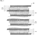
- FIG. 1 is a schematic cross-sectional view showing an example of the stacked battery of the present disclosure.
- Stacked battery 100 shown in FIG. 1 comprises plurality of cells 10 (10A, 10B to 10H to 10N) in a thickness direction; and each of plurality of cells 10 includes cathode current collector 4, cathode active material layer 1, solid electrolyte layer 3, anode active material layer 2, and anode current collector 5, in this order. Further, plurality of cells 10 are electrically connected in parallel.
- a method for connecting the cells in parallel is not particularly limited, and for example, cell 10A and cell 10B shown in FIG. 1 are connected in parallel in a manner that the cells share anode current collector 5.
- two cells next to each other may or may not share cathode current collector 4 or anode current collector 5.
- the two cells next to each other have cathode current collector 4 or anode current collector 5 individually between the cells.
- stacked battery 100 includes surface-side cell 10X that is located on a surface side of stacked battery 100, and center-side cell 10Y that is located on a center side rather than surface-side cell 10X. Further, stacked battery 100 features a configuration that a contact resistance between cathode current collector 4 and anode current collector 5 in surface-side cell 10X is more than a contact resistance between cathode current collector 4 and anode current collector 5 in center-side cell 10Y.
- the unevenness of short circuit resistance among the plurality of cells may be suppressed in the stacked battery.
- the present inventors have acquired new knowledge that the resistance of a short circuit part (short circuit resistance) in each cell varies greatly with the cell location.
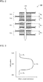
- FIG. 2 This new knowledge will be explained referring to FIG. 2 .
- nail 110 is penetrated into stacked battery 100 comprising plurality of cells 10 (10A, 10B to 10H to ION) electrically connected in parallel.
- short circuit resistance R R A , R B to R H to R N
- cell 10A located on the surface side has lower short circuit resistance compared to cell 10H located on the center side.
- the behavior of the short circuit resistance on the surface side that is opposite to the nail penetrating surface (such as location P 3 in FIG. 3 ) of the stacked battery may possibly vary with the constitution of the stacked battery; however, in both of the later described Reference Examples 1 and 2, the short circuit resistance was lowered. The reason therefor is presumed that, since the nail proceeds while dragging the larger amount of the fragment of each member, the cathode current collector and the anode current collector will be in a state electrically connected by the fragment with high electron conductivity.
- a contact resistance between the cathode current collector and the anode current collector in the surface-side cell is more than a contact resistance between the cathode current collector and the anode current collector in the center-side cell
- the unevenness of short circuit resistance among the plurality of cells may be suppressed in the stacked battery.
- an inclusive term of merely "current collector” may be used for a cathode current collector and an anode current collector.
- the problem of suppressing the unevenness of short circuit resistance among the plurality of cells is a problem never occurs in a single cell, that is, a problem peculiar to a stacked battery.
- a pressure applied to the stacked battery during a nail penetration test will be extremely high. Since a high pressure such as 100 MPa or more at the part where the nail penetrates, and particularly, 400 MPa or more at the tip part of the nail, is applied, the management of the short circuit resistance in a high pressure condition is important.
- the stacked battery of the present disclosure includes a surface-side cell that is located on a surface side of the stacked battery, and a center-side cell that is located on a center side rather than the surface-side cell. Further, a contact resistance between the cathode current collector and the anode current collector in the surface-side cell is more than a contact resistance between the cathode current collector and the anode current collector in the center-side cell. Particularly, the difference of the contact resistances in a high pressure condition (such as 100 MPa) is preferably large.
- the stacked battery of the present disclosure usually comprises two kinds or more of the cells with a different contact resistance between the cathode current collector and the anode current collector.
- surface-side cell and “center-side cell” in the present disclosure are stipulations for specifying the cells with a different contact resistance between the cathode current collector and the anode current collector.
- an assumed case is a stacked battery comprising two kinds of the cells (cell ⁇ and cell ⁇ ) with a different contact resistance between the cathode current collector and the anode current collector.
- the contact resistances are cell ⁇ > cell ⁇ .
- any one of the plurality of cells ⁇ may be specified as the surface-side cell.
- any one of the plurality of cells ⁇ may be specified as the center-side cell.
- the stacked battery comprises three kinds or more of the cells with a different contact resistance between the cathode current collector and the anode current collector, comparing two cells with a different contact resistance among them, when the magnitude relation of the contact resistances and the locational relation of the two cells satisfy the specific conditions, one cell is specified as the surface-side cell, and the other cell is specified as the center-side cell.
- the contact resistance between the cathode current collector and the anode current collector in the surface-side cell is regarded as R c1
- the contact resistance between the cathode current collector and the anode current collector in the center-side cell is regarded as R c2 .
- the value of R c1 /R c2 under pressure of 100 MPa is, for example, 1.5 or more, and may be 10 or more. Meanwhile, the value of R c1 /R c2 under pressure of 100 MPa is, for example, 10000 or less.
- the value of R c1 under pressure of 100 MPa is not particularly limited, and is, for example, 0.037 ⁇ cm 2 or more, may be 0.047 ⁇ cm 2 or more, and may be 0.103 ⁇ cm 2 or more. Meanwhile, the value of R c1 under pressure of 100 MPa is, for example, 0.277 ⁇ cm 2 or less. Incidentally, a method for measuring a contact resistance between the cathode current collector and the anode current collector will be explained in the later described Reference Example 1.
- the contact resistance between the cathode current collector and the anode current collector in the surface-side cell is more than the contact resistance between the cathode current collector and the anode current collector in the center-side cell.
- the contact resistance may be adjusted, for example, by at least one of the properties of the current collector, the properties of an oxide layer formed on a surface of the current collector, and the properties of a coating layer, containing a carbon material, formed on a surface of the current collector.
- the material for the cathode current collector in the surface-side cell may be different from the material for the cathode current collector in the center-side cell.
- the material for the anode current collector in the surface-side cell may be different from the material for the anode current collector in the center-side cell.
- the contact resistance between the cathode current collector and the anode current collector will be different.
- “Different material” refers to a case in which at least one of the followings in relation to the current collector is different: included elements, composition, and crystal state.
- the cathode current collectors may contain the same material whereas the anode current collectors may contain different materials; the cathode current collectors may contain different materials whereas the anode current collectors may contain the same material; and both of the cathode current collectors and the anode current collectors may contain different materials.
- At least one of the cathode current collector and the anode current collector in the surface-side cell may include, on a surface thereof, an oxide layer.
- a surface resistance increases by including the oxide layer, and the contact resistance between the cathode current collector and the anode current collector also increases.
- the oxide layer is preferably formed on at least the solid electrolyte layer facing side of the current collector.
- the oxide layer is preferably, for example, an oxide layer including the same metal element as the current collector.
- the thickness of the oxide layer is, for example, 10 nm or more, and may be 20 nm or more.
- the oxide layer is preferably an oxidation treated layer of the current collector.
- the oxidation treatment may include, for example, a heat treatment in the atmosphere.
- the heat treatment temperature is, for example, 150°C or more, and may be within a range of 200°C to 500°C.
- At least one of the cathode current collector and the anode current collector in the center-side cell may include, on a surface thereof, an oxide layer.
- the thickness of the oxide layer in the cathode current collector of the surface-side cell is preferably lager than the thickness of the oxide layer in the cathode current collector of the center-side cell.
- the thickness of the oxide layer in the anode current collector of the surface-side cell is preferably larger than the thickness of the oxide layer in the anode current collector of the center-side cell.
- the cathode current collector and the anode current collector in the center-side cell may not include the oxide layer on a surface thereof.
- At least one of the cathode current collector and the anode current collector in the surface-side cell may include, on a surface thereof, a coating layer containing a carbon material. Also, at least one of the cathode current collector and the anode current collector in the center-side cell may include, on a surface thereof, a coating layer containing a carbon material.
- the coating layer of the cathode current collector of the surface-side cell may be regarded as a first coating layer
- the coating layer of the cathode current collector of the center-side cell may be regarded as a second coating layer
- the coating layer of the anode current collector of the surface-side cell may be regarded as a third coating layer
- the coating layer of the anode current collector of the center-side cell may be regarded as a fourth coating layer, in some cases.
- the coating layer is a layer containing at least a carbon material, and may further contain a resin.
- the carbon material may include carbon blacks such as furnace black, acetylene black, Ketjen black, and thermal black; carbon fibers such as carbon nanotube and carbon nanofiber; activated carbon; carbon; graphite; graphene; and fullerene.
- the shape of the carbon material may include a granular shape.
- the resin may include a thermoplastic resin.
- the thermoplastic resin may include polyvinylidene fluorid (PVDF), polypropylene, polyethylene, polyvinyl chloride, polystyrene, acrylonitrile butadiene styrene (ABS) resin, methacrylic resin, polyamide, polyester, polycarbonate, and polyacetal.
- PVDF polyvinylidene fluorid
- ABS acrylonitrile butadiene styrene
- methacrylic resin polyamide
- polyester polycarbonate
- polyacetal polyacetal.
- the melting temperature of the resin is, for example, within a range of 80°C to 300°C.
- the thickness of the coating layer is, for example, within a range of 1 ⁇ m to 20 ⁇ m, and may be within a range of 1 ⁇ m to 10 ⁇ m.
- a content of the carbon material in the first coating layer may be less than a content of the carbon material in the second coating layer.
- a content of the carbon material in the third coating layer may be less than a content of the carbon material in the fourth coating layer.
- a surface resistance increases by decreasing the content of the carbon material in the coating layer of the surface-side cell, and the contact resistance between the cathode current collector and the anode current collector in the surface-side cell also increases.
- the content of the carbon material in the first coating layer or the third coating layer is, for example, 20% by volume or less, and may be 10% by volume or less.
- the cathode current collectors of the surface-side cell and the center-side cell may include the same material, whereas the contents of the carbon material in the coating layers may be different.
- the anode current collectors of the surface-side cell and the center-side cell may include the same material, whereas the contents of the carbon material in the coating layers may be different.
- a thickness of the first coating layer may be more than a thickness of the second coating layer.
- a thickness of the third coating layer may be more than a thickness of the fourth coating layer.
- the contact resistance between the cathode current collector and the anode current collector in the surface-side cell increases by increasing the thickness of the coating layer of the surface-side cell.
- the difference of the thicknesses of the first coating layer and the second coating layer is, for example, 1 ⁇ m or more, may be 3 ⁇ m or more, and may be 6 ⁇ m or more.
- the difference of the thicknesses of the third coating layer and the fourth coating layer is similar to the above.
- the cathode current collectors of the surface-side cell and the center-side cell may include the same material, whereas the thickness of the coating layers may be different.
- the anode current collectors of the surface-side cell and the center-side cell may include the same material, whereas the thicknesses of the coating layers may be different.
- the coating layer may or may not further contain an inorganic filler.
- a coating layer with high electron conductivity may be obtained
- a coating layer with PTC property may be obtained.
- PTC Positive Temperature Coefficient, and is a property whose resistance changes with a positive coefficient according to a temperature increase.
- the resin contained in the coating layer may possibly expand in its volume according to a temperature increase and cause a resistance increase of the coating layer.
- the resin influenced by the binding pressure deforms or flows so that sufficient PTC property cannot be exhibited in some cases.
- the binding pressure is, for example, 0.1 MPa or more, may be 1 MPa or more, and may be 5 MPa or more. Meanwhile, the binding pressure is, for example, 100 MPa or less, may be 50 MPa or less, and may be 20 MPa or less.
- Examples of the inorganic filler may include a metallic oxide and a metallic nitride.
- Examples of the metallic oxide may include alumina, zirconia, and silica, and examples of the metallic nitride may include silicon nitride.
- the average particle size (D 50 ) of the inorganic filler is, for example, within a range of 50 nm to 5 ⁇ m, and may be within a range of 100 nm to 2 ⁇ m.
- the content of the inorganic filler in the coating layer is, for example, 50% by volume or more, and may be 60% by volume or more. Meanwhile, the content of the inorganic filler in the coating layer is, for example, 85% by volume or less, and may be 80% by volume or less.
- the proportion of resistance R 200 of the coating layer at 200°C with respect to resistance R 25 of the coating layer at 25°C is regarded as R 200 /R 25 .
- the R 200 /R 25 value of the first coating layer may be more than the R 200 /R 25 value of the second coating layer.
- the R 200 /R 25 value of the third coating layer may be more than the R 200 /R 25 value of the fourth coating layer.
- the contact resistance between the cathode current collector and the anode current collector in the surface-side cell increases when the current breaking performance of the coating layer of the surface-side cell is high.
- the R 200 /R 25 value is preferably, for example, 10 or more.
- the cathode current collectors of the surface-side cell and the center-side cell may include the same material, whereas the current breaking performances of the coating layers may be different.
- the anode current collectors of the surface-side cell and the center-side cell may include the same material, whereas the current breaking performances of the coating layers may be different.
- one of the cathode current collector and the anode current collector in the surface-side cell may include, on a surface thereof, a coating layer containing a carbon material, and another may not include, on a surface thereof, a coating layer containing a carbon material; whereas one of the cathode current collector and the anode current collector in the center-side cell may include, on a surface thereof, a coating layer containing a carbon material, and another may not include, on a surface thereof, a coating layer containing a carbon material in reverse to the surface-side cell.
- both of the cathode current collectors and the anode current collectors of the surface-side cell and the center-side cell may include the same material, whereas the current collectors on which the coating layers are formed may be different.
- Each of the plurality of cells included in the stacked battery is numbered as a 1 st cell to a N th cell in order along the thickness direction of the stacked battery.
- N refers to the total cell number included in the stacked battery; for example, N is 3 or more, may be 10 or more, may be 30 or more, and may be 50 or more. Meanwhile, N is, for example, 200 or less, may be 150 or less, and may be 100 or less.
- the surface-side cell is preferably a cell that belongs to a cell region including the 1 st cell to a (N/3) th cell.
- the (N/3) th cell is a cell whose order corresponds to a value obtained by dividing the total cell number N by three. For example, when the total cell number is 60, the (N/3) th cell is a 20 th cell.
- the (N/3) th cell is specified by rounding off to the nearest integer.
- the surface-side cell may be, for example, a cell that belongs to a cell region including the 1 st cell to the 20 th cell, and may be a cell that belongs to a cell region including the 1 st cell to a 10 th cell.
- the surface-side cell may be, for example, a cell that belongs to a cell region including a 5 th cell to the (N/3) th cell, and may be a cell that belongs to a cell region including the 10 th cell to the (N/3) th cell.
- the surface-side cell may be specified, excluding the 1 st cell and the neighborhood cells.
- the center-side cell is a cell that is located on the center side rather than the surface-side cell.
- Center side refers to the central side in the thickness direction of the stacked cells.
- the center-side cell is preferably a cell that belongs to a cell region including a ((N/3) + 1) th cell to a (2N/3) th cell.
- the ((N/3) + 1) th cell refers to a cell next to the (N/3) th cell when numbered from the 1 st cell.
- the (2N/3) th cell is a cell whose order corresponds to a value obtained by dividing the doubled value of the total cell number N by three.
- the (2N/3) th cell is a 40 th cell.
- the (2N/3) th cell is specified by rounding off to the nearest integer.
- the center-side cell may be, for example, a cell that belongs to a cell region including the 21 st cell to the 40 th cell.
- a cell region including the 1 st cell to the (N/3) th cell is regarded as a cell region A
- a cell region including the ((N/3) + 1) th cell to the (2N/3) th cell is regarded as a cell region B.
- the average contact resistance R CA in the cell region A is preferably more than the average contact resistance R CB in the cell region B.
- the value of R CA /R CB under pressure of 100 MPa is, for example, 1.5 or more, and may be 10 or more. Meanwhile, the value of R CA /R CB under pressure of 100 MPa is, for example, 10000 or less.
- a cell region including the 1 st cell to the 20 th cell is regarded as a cell region C
- a cell region including the 21 st cell to the 40 th cell is regarded as a cell region D.
- the average contact resistance R CC in the cell region C is preferably more than the average contact resistance R CD in the cell region D.
- the value of R CC /R CD under pressure of 100 MPa is, for example, 1.5 or more, and may be 10 or more. Meanwhile, the value of R CC /R CD under pressure of 100 MPa is, for example, 10000 or less.
- the contact resistance between the cathode current collector and the anode current collector, under pressure of 100 MPa, in all of the plurality of cells may be 0.037 ⁇ cm 2 or more, may be 0.047 ⁇ cm 2 or more, and may be 0.103 ⁇ cm 2 or more.
- the short circuit resistance of the cell with the lowest short circuit resistance is regarded as R Min
- the short circuit resistance of the cell with the highest short circuit resistance is regarded as R Max .
- R Min the short circuit resistance of the cell with the lowest short circuit resistance
- R Max the short circuit resistance of the cell with the highest short circuit resistance
- the value of R Max /R Min is preferably 100 or less, and more preferably 5.0 or less.
- the nail penetration test is carried out under conditions mentioned in the later described Reference Examples 1 and 2.
- the cell in the present disclosure includes a cathode current collector, a cathode active material layer, a solid electrolyte layer, an anode active material layer, and an anode current collector, in this order.
- the cell is typically a cell utilizing Li ion conductivity (a Li ion cell). Also, the cell is preferably a cell capable of being charged and discharged (a secondary battery).
- the anode active material layer includes at least an anode active material, and may include at least one of a solid electrolyte material, a conductive material, and a binder as required.
- the anode active material is not particularly limited, and examples thereof may include a metal active material, a carbon active material, and an oxide active material.
- the metal active material may include a simple substance of metal and a metal alloy.
- the metal element included in the metal active material may include Si, Sn, In, and Al.
- the metal alloy is preferably an alloy including the above described metal element as the main component.
- the Si alloy may include a Si-Al base alloy, a Si-Sn base alloy, a Si-In base alloy, a Si-Ag base alloy, a Si-Pb base alloy, a Si-Sb base alloy, a Si-Bi base alloy, a Si-Mg base alloy, a Si-Ca base alloy, a Si-Ge base alloy, and a Si-Pb base alloy.
- the Si-Al based alloy for example, refers to an alloy including at least Si and Al, may be an alloy including only Si and Al, and may be an alloy further including an additional metal element. It is much the same for the alloys other than the Si-Al based alloy.
- the metal alloy may be a two-component based alloy, and may be a multicomponent based alloy including three or more components.
- examples of the carbon active material may include a mesocarbon microbead (MCMB), a highly oriented pyrolytic graphite (HOPG), a hard carbon, and a soft carbon.
- examples of the oxide active material may include a lithium titanate such as Li 4 Ti 5 O 12 .
- Examples of the shape of the anode active material may include a granular shape.
- the average particle size (D 50 ) of the anode active material is, for example, within a range of 10 nm to 50 ⁇ m, and may be within a range of 100 nm to 20 ⁇ m.
- the proportion of the anode active material in the anode active material layer is, for example, 50% by weight or more, and may be within a range of 60% by weight to 99% by weight.
- the solid electrolyte material is not particularly limited, and examples thereof may include an inorganic solid electrolyte material such as a sulfide solid electrolyte material, and an oxide solid electrolyte material.
- the sulfide solid electrolyte material may include Li 2 S-P 2 S 5 , Li 2 S-P 2 S 5 -LiI, Li 2 S-P 2 S 5 -LiI-LiBr, Li 2 S-P 2 S 5 -Li 2 O, Li 2 S-P 2 S 5 -Li 2 O-LiI, Li 2 S-SiS 2 , Li 2 S-SiS 2 -LiI, Li 2 S-SiS 2 -LiBr, Li 2 S-SiS 2 -LiCl, Li 2 S-SiS 2 -B 2 S 3 -LiI, Li 2 S-SiS 2 -P 2 S 5 -LiI, Li 2 S-B 2 S 3 , Li 2 S-
- the sulfide solid electrolyte material is preferably provided with an ion conductor including Li, A (A is at least one kind of P, Si, Ge, Al, and B), and S.
- the ion conductor preferably includes an anion structure (PS 4 3- structure, SiS 4 4- structure, GeS 4 4- structure, AlS 3 3- structure, BS 3 3- structure) of an ortho-composition, as the main component of an anion.
- the reason therefor is to obtain a sulfide solid electrolyte material with high chemical stability.
- the proportion of the anion structure of the ortho-composition among the total anion structures in the ion conductor is preferably 70 mol% or more, and more preferably 90 mol% or more.
- the proportion of the anion structure of the ortho-composition may be determined by, for example, a Raman spectroscopy, a NMR, and an XPS.
- the sulfide solid electrolyte material may include a lithium halide.
- the lithium halide may include LiF, LiCl, LiBr, and LiI, and among them, LiCl, LiBr, and LiI are preferable.
- the solid electrolyte material may be a crystalline material, and may be an amorphous material. Also, the solid electrolyte material may be a glass, and may be a crystallized class (a glass ceramic). Examples of the shape of the solid electrolyte material may include a granular shape.
- Examples of the conductive material may include carbon materials such as acetylene black (AB), Ketjen black (KB), carbon fiber, carbon nanotube (CNT), and carbon nanofiber (CNF).
- examples of the binder may include rubber based binders such as butylene rubber (BR), styrenebutadiene rubber (SBR); and fluoride based binders such as polyvinylidene fluoride (PVDF).
- the thickness of the anode active material layer is, for example, within a range of 0.1 ⁇ m to 300 ⁇ m, and may be within a range of 0.1 ⁇ m to 100 ⁇ m.
- the cathode active material layer includes at least a cathode active material, and may include at least one of a solid electrolyte material, a conductive material, and a binder as required.
- the cathode active material is not particularly limited, and examples thereof may include an oxide active material.
- the oxide active material may include a rock salt bed type active material such as LiCoO 2 , LiMnO 2 , LiNiO 2 , LiVO 2 , and LiNi 1/3 Co 1/3 Mn 1/3 O 2 ; a spinel type active material such as LiMn 2 O 4 , Li 4 Ti 5 O 12 , and Li(Ni 0.5 Mn 1.5 )O 4 ; and an olivine type active material such as LiFePO 4 , LiMnPO 4 , LiNiPO 4 , and LiCoPO 4 .
- oxide active material for example, a LiMn spinel active material represented by Li 1+x Mn 2-x-y M y O 4 (M is at least one kind of Al, Mg, Co, Fe, Ni, and Zn, and 0 ⁇ x + y ⁇ 2), and a lithium titanate may be used.
- M is at least one kind of Al, Mg, Co, Fe, Ni, and Zn, and 0 ⁇ x + y ⁇ 2
- a coating layer including a Li ion conductive oxide may be formed on a surface of the cathode active material.
- the reason therefore is to suppress the reaction between the cathode active material and the solid electrolyte material.
- the Li ion conductive oxide may include LiNbO 3 , Li 4 Ti 5 O 12 , and Li 3 PO 4 .
- the thickness of the coating layer is, for example, within a range of 0.1 nm to 100 nm, and may be within a range of 1 nm to 20 nm.
- the coverage of the coating layer on the cathode active material surface is, for example, 50% or more, and may be 80% or more.
- the solid electrolyte material, the conductive material, and the binder used for the cathode active material layer are respectively in the same contents as those described in "(1) Anode active material layer" above; thus, the descriptions herein are omitted.
- the thickness of the cathode active material layer is, for example, within a range of 0.1 ⁇ m to 300 ⁇ m, and may be within a range of 0.1 ⁇ m to 100 ⁇ m.
- the solid electrolyte layer is a layer formed between the cathode active material layer and the anode current collector. Also, the solid electrolyte layer includes at least a solid electrolyte material, and may further include a binder as required.
- the solid electrolyte material and the binder used for the solid electrolyte layer are respectively in the same contents as those described in "(1) Anode active material layer" above; thus, the descriptions herein are omitted.
- the content of the solid electrolyte material in the solid electrolyte layer is, for example, within a range of 10% by weight to 100% by weight, and may be within a range of 50% by weight to 100% by weight.
- the thickness of the solid electrolyte layer is, for example, within a range of 0.1 ⁇ m to 300 ⁇ m, and may be within a range of 0.1 ⁇ m to 100 ⁇ m.
- the cathode current collector collects currents of the above described cathode active material layer, and the anode current collector collects currents of the above described anode active material layer.
- the metal element included in the cathode current collector is not particularly limited, and examples thereof may include Al, Fe, Ti, Ni, Zn, Cr, Au, and Pt.
- the cathode current collector may be a simple substance of the metal element, and may be an alloy including the metal element as the main component.
- Stainless steel (SUS) is an example of the Fe alloy, and SUS304 is preferable.
- Examples of the shape of the cathode current collector may include a foil shape and a mesh shape.
- the thickness of the cathode current collector is, for example, 0.1 ⁇ m or more, and may be 1 ⁇ m or more. When the cathode current collector is too thin, the current collecting function may be degraded. Meanwhile, the thickness of the cathode current collector is, for example, 1 mm or less, and may be 100 ⁇ m or less. When the cathode current collector is too thick, the energy density of a battery may be degraded.
- the metal element included in the anode current collector is not particularly limited, and examples thereof may include Cu, Fe, Ti, Ni, Zn, and Co.
- the anode current collector may be a simple substance of the metal element, and may be an alloy including the metal element as the main component.
- Stainless steel (SUS) is an example of the Fe alloy, and SUS304 is preferable.
- Examples of the shape of the anode current collector may include a foil shape and a mesh shape.
- the thickness of the anode current collector is, for example, 0.1 ⁇ m or more, and may be 1 ⁇ m or more. When the anode current collector is too thin, the current collecting function may be degraded. Meanwhile, the thickness of the anode current collector is, for example, 1 mm or less, and may be 100 ⁇ m or less. When the anode current collector is too thick, the energy density of a battery may be degraded.
- the present disclosure is not limited to the embodiments.
- the embodiments are exemplification, and any other variations are intended to be included in the technical scope of the present disclosure if they have substantially the same constitution as the technical idea described in the claim of the present disclosure and offer similar operation and effect thereto.
- the cathode active material Li 1.15 Ni 1/3 Co 1/3 Mn 1/3 W 0.005 O 2
- LiNbO 3 Li 1.15 Ni 1/3 Co 1/3 Mn 1/3 W 0.005 O 2
- a PVDF based binder manufactured by Kureha Corp.
- the PP container was stirred for 30 seconds by an ultrasonic dispersion apparatus (UH-50, manufactured by SMT Corp.)
- the PP container was agitated for 3 minutes by an agitation mixer (TTM-1, manufactured by Sibata Scientific Technology LTD.), and further, was stirred for 30 seconds by the ultrasonic dispersion apparatus to obtain a coating solution.
- an Al foil manufactured by Nippon Foil Mfg. Co. Ltd., a cathode current collector
- the obtained coating solution was pasted on the Al foil by a blade method using an applicator.
- the coated electrode was dried naturally, and then, was dried at 100°C for 30 minutes on a hot plate to form a cathode active material layer on one surface of the cathode current collector.
- the obtained product was cut according to the size of the battery to obtain a cathode.
- a PVDF based binder manufactured by Kureha Corp.
- a conductive material
- a Cu foil (anode current collector 5) was prepared.
- the obtained coating solution was pasted on the Cu foil by a blade method using an applicator.
- the coated electrode was dried naturally, and then, was dried at 100°C for 30 minutes on a hot plate.
- anode active material layer 2 was formed on one surface of the Cu foil (anode current collector 5).
- anode active material layer 2 was formed on another surface of the Cu foil (anode current collector 5) as shown in FIG. 6C .
- the obtained product was cut according to the size of the battery to obtain an anode.
- the PP container was stirred for 30 seconds by an ultrasonic dispersion apparatus (UH-50, manufactured by SMT Corp.).
- the PP container was agitated for 30 minutes by an agitation mixer (TTM-1, manufactured by Sibata Scientific Technology LTD.), and further, was stirred for 30 seconds by the ultrasonic dispersion apparatus to obtain a coating solution.
- an Al foil manufactured by Nippon Foil Mfg. Co. Ltd.
- the obtained coating solution was pasted on the Al foil by a blade method using an applicator.
- the coated electrode was dried naturally, and then, was dried at 100°C for 30 minutes on a hot plate.
- the obtained product was cut according to the size of the battery to obtain a transfer member including the Al foil and the solid electrolyte layer.
- Each of the two obtained transfer members was placed on the anode active material layers formed on the both sides of the anode current collector, and the product was pressed under the pressure of 4 ton/cm 2 by a cold isostatic pressing method (CIP method). After that, the Al foils of the transfer members were peeled off. Thereby, as shown in FIG. 6D , solid electrolyte layers 3 were formed on anode active material layers 2.
- each of the two above obtained cathodes was placed on the solid electrolyte layers formed on the both sides of the anode current collectors, and the product was pressed under the pressure of 4 ton/cm 2 by the cold isostatic pressing method (CIP method).
- cathode active material layers 1 and cathode current collectors 4 were formed on solid electrolyte layers 3. As described above, a two-stacked cell was obtained. Further, 30 of the obtained two-stacked cells were stacked, and the obtained product was sealed with an aluminum laminate film to obtain an evaluation battery.
- a PVDF based binder manufactured by Kureha Corp.
- a sulfide solid electrolyte material Li 2 S-P 2 S 5 based glass ceramic including LiI and Li
- the PP container was stirred for 30 seconds by an ultrasonic dispersion apparatus (UH-50, manufactured by SMT Corp.)
- the PP container was agitated for 30 minutes by an agitation mixer (TTM-1, manufactured by Sibata Scientific Technology LTD.), and further, was stirred for 30 seconds by the ultrasonic dispersion apparatus to obtain a coating solution.
- a two-stacked cell was obtained in the same manner as in Reference Example 1 except that the obtained coating solution was used. Further, an evaluation battery was obtained in the same manner as in Reference Example 1 except that 40 of the obtained two-stacked cells were stacked.
- Nail SK (carbon tool steel) material ( ⁇ : 8 mm, tip angle: 60°)
- the short circuit resistance of a cell was obtained from a voltage profile upon the nail penetration.
- An example of the voltage profile is shown in FIG. 7 .
- the voltage of the cell decreases by penetrating the nail.
- the initial voltage is referred to as V 0
- the minimum voltage upon the nail penetration is referred to as V.
- the internal resistance of the cell was measured in advance, and the internal resistance is referred to as r.
- the short circuit resistance of the cell is referred to as R.
- the short circuit resistance R of the cell may be calculated from this relationship.
- the short circuit resistance of the 1 st cell was more than the short circuit resistance of the 10 th cell. The reason therefor is presumed that upon the nail penetration, the insulating part of the laminate film was dragged in.
- the short circuit resistance of the 40 th cell was more compared to the short circuit resistance of the 1 st cell or the 10 th cell
- the short circuit resistance of the 60 th cell was more compared to the short circuit resistance of the 1 st cell or the 10 th cell.
- the short circuit resistance was less in the surface-side cell, and was more in the center-side cell.
- Reference Example 1 in which Si was used as the anode active material the unevenness of the short circuit resistance was extremely large compared to Reference Example 2 in which C was used as the anode active material.
- An Al foil (15 ⁇ m thickness, 1N30 manufactured by UACJ Corp.) was prepared as a cathode current collector, and a Cu foil (12 ⁇ m thickness, electrolytic Cu foil manufactured by Furukawa Electric Co., Ltd.) was prepared as an anode current collector.
- a SUS foil (SUS304, 15 ⁇ m thickness, manufactured by Toyo Seihaku Co., Ltd.) was prepared as a cathode current collector, and a Cu foil (12 ⁇ m thickness, electrolytic Cu foil manufactured by Furukawa Electric Co., Ltd.) was prepared as an anode current collector.
- An Al foil (15 ⁇ m thickness, 1N30 manufactured by UACJ Corp.) was prepared as a cathode current collector, and a Fe foil (10 ⁇ m thickness, manufactured by Takeuchi Kinzoku Hakufun Kogyo Co., Ltd.) was prepared as an anode current collector.
- the contact resistance between the cathode current collector and the anode current collector each prepared in Experimental Examples 1 to 5 was measured. Specifically, as shown in FIG. 8 , anode current collector 5 was placed on bakelite plate 21, kapton film 22 having a through section was placed on anode current collector 5, and cathode current collector 4 was placed on kapton film 22. Further, SK material block 23 with ⁇ 11.28 mm was placed on cathode current collector 4 so as to overlap the through section of kapton film 22 in plan view. In this situation, the resistance value, when 100 MPa was applied by autograph 24, was measured by a resistance meter (RM3542, manufactured by Hioki E. E. Corp.). The results thereof are shown in Table 3.
- a heat treatment was conducted to a SUS foil (SUS304, 15 ⁇ m thickness, manufactured by Toyo Seihaku Co., Ltd.) under the condition of 200°C for 1 hour, in the atmosphere, and an oxide layer (oxide layer of SUS) was formed on a surface thereof.
- the obtained SUS foil was prepared as a cathode current collector, and a Cu foil (12 ⁇ m thickness, electrolytic Cu foil manufactured by Furukawa Electric Co., Ltd.) was prepared as an anode current collector.
- a heat treatment was conducted to a SUS foil (SUS304, 15 ⁇ m thickness, manufactured by Toyo Seihaku Co., Ltd.) under the condition of 500°C for 1 hour, in the atmosphere, and an oxide layer (oxide layer of SUS) was formed on a surface thereof.
- the obtained SUS foil was prepared as a cathode current collector, and a Cu foil (12 ⁇ m thickness, electrolytic Cu foil manufactured by Furukawa Electric Co., Ltd.) was prepared as an anode current collector.
- the contact resistance was increased by forming the oxide layer on the surface of the current collector. From these results, it was suggested that, by forming the oxide layer on the current collector of the surface-side cell, the short circuit resistance of the surface-side cell may be increased, and as the result, the unevenness of short circuit resistance among a plurality of cells may be suppressed.
- a pressure applied to the stacked battery during a nail penetration test will be extremely high.
- a high pressure such as 100 MPa or more is applied to the part where the nail penetrates. Since the situations in a high pressure condition (such as 100 MPa or more) and low pressure condition (such as 1 MPa) are completely different, it is difficult to predict the short circuit resistance in a high pressure condition, based on the short circuit resistance in a low pressure condition.
- NMP N-methylpyrrolidone
- PVDF KF polymer L#9130, manufactured by Kureha Corp.
- An Al foil (15 ⁇ m thickness, 1N30 manufactured by UACJ Corp.) was coated with the obtained paste so as the thickness after drying to be 10 ⁇ m, dried in a drying furnace, and a coating layer was formed.
- the obtained Al foil was prepared as a cathode current collector, and a Cu foil (12 ⁇ m thickness, electrolytic Cu foil manufactured by Furukawa Electric Co., Ltd.) was prepared as an anode current collector.
- the obtained Al foil was prepared as a cathode current collector, and a Cu foil (12 ⁇ m thickness, electrolytic Cu foil manufactured by Furukawa Electric Co., Ltd.) was prepared as an anode current collector.
- the obtained Al foil was prepared as a cathode current collector, and a Cu foil (12 ⁇ m thickness, electrolytic Cu foil manufactured by Furukawa Electric Co., Ltd.) was prepared as an anode current collector.
- NMP N-methylpyrrolidone
- PVDF KF polymer L#9130, manufactured by Kureha Corp.
- An Al foil (15 ⁇ m thickness, 1N30 manufactured by UACJ Corp.) was coated with the obtained paste so as the thickness after drying to be 3 ⁇ m, dried in a drying furnace, and a coating layer was formed.
- the obtained Al foil was prepared as a cathode current collector, and a Cu foil (12 ⁇ m thickness, electrolytic Cu foil manufactured by Furukawa Electric Co., Ltd.) was prepared as an anode current collector.
- a coating layer was formed in the same manner as in Experimental Example 11 except that the thickness of the coating layer was changed to 6 ⁇ m.
- the obtained Al foil was prepared as a cathode current collector, and a Cu foil (12 ⁇ m thickness, electrolytic Cu foil manufactured by Furukawa Electric Co., Ltd.) was prepared as an anode current collector.
- a coating layer was formed in the same manner as in Experimental Example 11 except that the thickness of the coating layer was changed to 9 ⁇ m.
- the obtained Al foil was prepared as a cathode current collector, and a Cu foil (12 ⁇ m thickness, electrolytic Cu foil manufactured by Furukawa Electric Co., Ltd.) was prepared as an anode current collector.
- a coating layer was formed in the same manner as in Experimental Example 11 except that the thickness of the coating layer was changed to 12 ⁇ m.
- the obtained Al foil was prepared as a cathode current collector, and a Cu foil (12 ⁇ m thickness, electrolytic Cu foil manufactured by Furukawa Electric Co., Ltd.) was prepared as an anode current collector.
- NMP N-methylpyrrolidone
- a conductive material furnace black, average primary particle size of 66 nm, manufactured by Tokai Carbon Co., Ltd.
- a filler alumina, CB-P02 manufactured by Showa Denko K. K.
- PVDF KF polymer L#9130, manufactured by Kureha Corp.
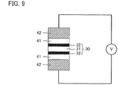
- test piece 30 including current collector (Al foil) 31 and coating layers 32 formed on the both sides thereof was prepared, Al foil 41 and SK material block 42 were placed in sequence on each of the two coating layers 32, and was bound by 60 MPa.
- a direct current was supplied in this situation, the resistance was determined from the change in voltage at that time.
- the measurement was conducted in an electric furnace, and the temperatures in the electric furnace were 25°C and 200°C.
- the results thereof are shown in Table 7. Incidentally, the resistance values in Table 7 are relative values when the resistance in Experimental Example 15 at 25°C is 1. [Table 7] Current collector Resistance Kind Coating composition (vol.
- NMP N-methylpyrrolidone
- a conductive material furnace black, average primary particle size of 66 nm, manufactured by Tokai Carbon Co., Ltd.
- a filler alumina, CB-P02 manufactured by Showa Denko K. K.
- PVDF KF polymer L#9130, manufactured by Kureha Corp.
- a Cu foil (12 ⁇ m thickness, electrolytic Cu foil manufactured by Furukawa Electric Co., Ltd.) was coated with the obtained paste so as the thickness after drying to be 10 ⁇ m, dried in a drying furnace, and a coating layer was formed.
- the obtained Cu foil was prepared as an anode current collector.
- An Al foil (15 ⁇ m thickness, 1N30 manufactured by UACJ Corp.) was coated with the obtained paste so as the thickness after drying to be 10 ⁇ m, dried in a drying furnace, and a coating layer was formed.
- the obtained Al foil was prepared as a cathode current collector.
- a Cu foil (12 ⁇ m thickness, electrolytic Cu foil manufactured by Furukawa Electric Co., Ltd.) was prepared as an anode current collector.
Landscapes
- Chemical & Material Sciences (AREA)
- Engineering & Computer Science (AREA)
- Chemical Kinetics & Catalysis (AREA)
- Electrochemistry (AREA)
- General Chemical & Material Sciences (AREA)
- Manufacturing & Machinery (AREA)
- Materials Engineering (AREA)
- Composite Materials (AREA)
- General Physics & Mathematics (AREA)
- Inorganic Chemistry (AREA)
- Condensed Matter Physics & Semiconductors (AREA)
- Physics & Mathematics (AREA)
- Secondary Cells (AREA)
- Battery Electrode And Active Subsutance (AREA)
- Connection Of Batteries Or Terminals (AREA)
- Cell Electrode Carriers And Collectors (AREA)
Claims (16)
- Batterie empilée (100) comprenant :une pluralité de cellules (10) dans le sens de l'épaisseur,la pluralité de cellules (10) étant électriquement connectées en parallèle ;chacune de la pluralité de cellules (10) comprenant un collecteur de courant de cathode (4), une couche de matériau actif de cathode (1), une couche d'électrolyte solide (3), une couche de matériau actif d'anode (2) et un collecteur de courant d'anode (5), dans cet ordre ;la batterie empilée (100) comprenant une cellule côté surface (10X) qui est située sur un côté surface de la batterie empilée (100) et une cellule côté central (10Y) qui est située sur un côté central plutôt que la cellule côté surface (10X) ; et caractérisée en ce queune résistance de contact entre le collecteur de courant de cathode (4) et le collecteur de courant d'anode (5) dans la cellule côté surface (10X) étant plus qu'une résistance de contact entre le collecteur de courant de cathode (4) et le collecteur de courant d'anode (5) dans la cellule côté central (10Y).
- Batterie empilée (100) selon la revendication 1, caractérisée en ce que le collecteur de courant de cathode (4) et/ou le collecteur de courant d'anode (5) dans la cellule côté surface (10X) comprend, sur une surface de celui-ci, une couche d'oxyde.
- Batterie empilée (100) selon la revendication 1, caractérisée en ce que le collecteur de courant de cathode (4) dans la cellule côté surface (10X) comprend, sur une surface de celui-ci, une première couche de revêtement contenant un matériau carboné, et
le collecteur de courant de cathode (4) dans la cellule côté central (10Y) comprend, sur une surface de celui-ci, une deuxième couche de revêtement contenant un matériau carboné. - Batterie empilée (100) selon la revendication 3, caractérisée en ce qu'une teneur du matériau carboné dans la première couche de revêtement est inférieure à une teneur du matériau carboné dans la deuxième couche de revêtement.
- Batterie empilée (100) selon la revendication 3 ou 4, caractérisée en ce qu'une épaisseur de la première couche de revêtement est supérieure à une épaisseur de la deuxième couche de revêtement.
- Batterie empilée (100) selon l'une quelconque des revendications 3 à 5, caractérisée en ce que, la valeur R200/R25 de la première couche de revêtement est supérieure à la valeur R200/R25 de la deuxième couche de revêtement, R200/R25 étant une proportion d'une résistance R200 à 200 °C de la couche de revêtement respective par rapport à une résistance R25 à 25 °C de la couche de revêtement respective.
- Batterie empilée (100) selon l'une quelconque des revendications 1 à 6, caractérisée en ce que le collecteur de courant d'anode (5) dans la cellule côté surface (10X) comprend, sur une surface de celui-ci, une troisième couche de revêtement contenant un matériau carboné, et
le collecteur de courant d'anode (5) dans la cellule côté central (10Y) comprend, sur une surface de celui-ci, une quatrième couche de revêtement contenant un matériau carboné. - Batterie empilée (100) selon la revendication 7, caractérisée en ce qu'une teneur du matériau carboné dans la troisième couche de revêtement est inférieure à une teneur du matériau carboné dans la quatrième couche de revêtement.
- Batterie empilée (100) selon la revendication 7 ou 8, caractérisée en ce qu'une épaisseur de la troisième couche de revêtement est supérieure à une épaisseur de la quatrième couche de revêtement.
- Batterie empilée (100) selon l'une quelconque des revendications 7 à 9, caractérisée en ce que, la valeur R200/R25 de la troisième couche de revêtement est supérieure à la valeur R200/R25 de la quatrième couche de revêtement, R200/R25 étant une proportion d'une résistance R200 à 200 °C de la couche de revêtement respective par rapport à une résistance R25 à 25 °C de la couche de revêtement respective.
- Batterie empilée (100) selon la revendication 1, caractérisée en ce que : le collecteur de courant de cathode (4) ou le collecteur de courant d'anode (5) dans la cellule côté surface (10X) comprend, sur une surface de celui-ci, une couche de revêtement contenant un matériau carboné, et une autre ne comprend pas, sur une surface de celui-ci, une couche de revêtement contenant un matériau carboné ; et
le collecteur de courant de cathode (4) ou le collecteur de courant d'anode (5) dans la cellule côté central (10Y) comprend, sur une surface de celui-ci, une couche de revêtement contenant un matériau carboné, et un autre ne comprend pas, sur une surface de celui-ci, une couche de revêtement contenant un matériau carboné à l'inverse de la cellule côté surface. - Batterie empilée (100) selon l'une quelconque des revendications 1 à 11, caractérisée en ce que, lorsque chacune de la pluralité de cellules (10) est numérotée en tant que la 1ère cellule à la nième cellule, où N ≥ 3, dans l'ordre dans le sens de l'épaisseur de la batterie empilée (100),
la cellule côté surface (10X) est une cellule qui appartient à une région cellulaire A comprenant la 1ère cellule à la (N/3)ième cellule. - Batterie empilée (100) selon la revendication 12, caractérisée en ce que la cellule côté central est une cellule (10Y) qui appartient à une région cellulaire B comprenant la ((N/3) + 1)ième cellule à la (2N/3)ième cellule, de préférence
caractérisée en ce qu'une valeur moyenne de la résistance de contact dans la région cellulaire A est supérieure à une valeur moyenne de la résistance de contact dans la région cellulaire B. - Batterie empilée (100) selon l'une quelconque des revendications 1 à 11, caractérisée en ce que, lorsque chacune de la pluralité de cellules (10) est numérotée en tant que la 1ère cellule à la Nième cellule, où N ≥ 60, dans l'ordre dans le sens de l'épaisseur de la batterie empilée (100),
la cellule côté surface (10X) est une cellule qui appartient à une région cellulaire C comprenant la 1ère cellule à la 20ième cellule. - Batterie empilée (100) selon la revendication 14, caractérisée en ce que la cellule côté central (10Y) est une cellule qui appartient à une région cellulaire D comprenant la cellule 21ième cellule à la 40ième cellule, de préférence
caractérisée en ce qu'une valeur moyenne de la résistance de contact dans la région cellulaire C est supérieure à une valeur moyenne de la résistance de contact dans la région cellulaire D. - Batterie empilée (100) selon l'une quelconque des revendications 1 à 15, caractérisée en ce que la couche de matériau actif d'anode (5) comprend Si ou un alliage de Si en tant que matériau actif d'anode.
Applications Claiming Priority (1)
| Application Number | Priority Date | Filing Date | Title |
|---|---|---|---|
| JP2017090091A JP6729481B2 (ja) | 2017-04-28 | 2017-04-28 | 積層電池 |
Publications (2)
| Publication Number | Publication Date |
|---|---|
| EP3396751A1 EP3396751A1 (fr) | 2018-10-31 |
| EP3396751B1 true EP3396751B1 (fr) | 2019-10-30 |
Family
ID=61971979
Family Applications (1)
| Application Number | Title | Priority Date | Filing Date |
|---|---|---|---|
| EP18166864.1A Active EP3396751B1 (fr) | 2017-04-28 | 2018-04-11 | Batterie empilée |
Country Status (8)
| Country | Link |
|---|---|
| US (1) | US11302953B2 (fr) |
| EP (1) | EP3396751B1 (fr) |
| JP (1) | JP6729481B2 (fr) |
| KR (1) | KR102055548B1 (fr) |
| CN (1) | CN108808111B (fr) |
| BR (1) | BR102018008016A2 (fr) |
| MY (1) | MY193479A (fr) |
| RU (1) | RU2679900C1 (fr) |
Families Citing this family (26)
| Publication number | Priority date | Publication date | Assignee | Title |
|---|---|---|---|---|
| JP6729479B2 (ja) | 2017-04-28 | 2020-07-22 | トヨタ自動車株式会社 | 積層電池 |
| JP6638693B2 (ja) | 2017-04-28 | 2020-01-29 | トヨタ自動車株式会社 | 積層電池 |
| JP6638692B2 (ja) | 2017-04-28 | 2020-01-29 | トヨタ自動車株式会社 | 積層電池 |
| KR102303678B1 (ko) | 2019-02-12 | 2021-09-16 | 도요타 지도샤(주) | 전고체 전지 적층체 |
| JP7211165B2 (ja) * | 2019-03-01 | 2023-01-24 | トヨタ自動車株式会社 | 全固体電池及びその製造方法 |
| JP7767152B2 (ja) * | 2019-06-03 | 2025-11-11 | エネヴェート・コーポレーション | 集電体上に炭素-ケイ素複合体を形成する方法 |
| CN112397765B (zh) * | 2019-08-16 | 2024-04-19 | 通用汽车环球科技运作有限责任公司 | 具有含电子导电聚合物的电极的固态电池 |
| GB2588939B (en) | 2019-11-15 | 2022-12-28 | Dyson Technology Ltd | Sputter deposition apparatus and method |
| GB2588947B (en) | 2019-11-15 | 2024-02-21 | Dyson Technology Ltd | A method of manufacturing solid state battery cathodes for use in batteries |
| GB2588935B (en) | 2019-11-15 | 2022-09-07 | Dyson Technology Ltd | Method and apparatus for sputter deposition of target material to a substrate |
| GB2588932B (en) | 2019-11-15 | 2022-08-24 | Dyson Technology Ltd | Method and apparatus for sputter deposition of target material to a substrate |
| GB2588946B (en) | 2019-11-15 | 2022-08-17 | Dyson Technology Ltd | Method of manufacturing crystalline material from different materials |
| GB2588940B (en) | 2019-11-15 | 2022-06-22 | Dyson Technology Ltd | Sputter deposition |
| GB2588944B (en) | 2019-11-15 | 2022-08-17 | Dyson Technology Ltd | Method of forming crystalline layer, method of forming a battery half cell |
| EP4178801A4 (fr) | 2020-07-07 | 2024-07-24 | Celgard, LLC | Membranes multicouches poreuses améliorées et procédés de fabrication de telles membranes |
| CN112151851B (zh) * | 2020-10-30 | 2022-03-29 | 珠海冠宇电池股份有限公司 | 一种能够降低内部温升的叠片式锂离子电池用叠芯 |
| JP7371611B2 (ja) * | 2020-12-02 | 2023-10-31 | トヨタ自動車株式会社 | 全固体電池 |
| JP7615641B2 (ja) * | 2020-12-02 | 2025-01-17 | トヨタ自動車株式会社 | 全固体電池 |
| US20240329146A1 (en) * | 2021-07-23 | 2024-10-03 | Celgard, Llc | Improved batteries, cells, components, and testing thereof |
| JP7524874B2 (ja) * | 2021-09-27 | 2024-07-30 | トヨタ自動車株式会社 | 全固体電池 |
| KR102951385B1 (ko) * | 2021-11-10 | 2026-04-10 | 주식회사 엘지에너지솔루션 | 전지셀 측면의 관통 시험 장치 및 이를 이용한 전지셀의 관통 시험 방법 |
| WO2023091474A1 (fr) * | 2021-11-17 | 2023-05-25 | Celgard, Llc | Séparateurs de batterie et leurs procédés de test |
| WO2023102909A1 (fr) * | 2021-12-10 | 2023-06-15 | 宁德时代新能源科技股份有限公司 | Élément de batterie, ensemble de batteries, bloc-batterie et dispositif électrique |
| WO2024057052A1 (fr) * | 2022-09-15 | 2024-03-21 | 日産自動車株式会社 | Batterie tout solide |
| KR102633827B1 (ko) * | 2022-12-09 | 2024-02-06 | 주식회사 포투원 | 해수를 사용하는 이차 배터리 팩 |
| JP7616264B2 (ja) * | 2023-04-05 | 2025-01-17 | トヨタ自動車株式会社 | 負極活物質層、及び固体二次電池 |
Family Cites Families (32)
| Publication number | Priority date | Publication date | Assignee | Title |
|---|---|---|---|---|
| JP3765094B2 (ja) * | 1996-12-28 | 2006-04-12 | 株式会社ジーエス・ユアサコーポレーション | 非水電解液電池 |
| JP5205713B2 (ja) | 2006-05-01 | 2013-06-05 | 日産自動車株式会社 | 双極型二次電池 |
| US8148010B2 (en) * | 2006-11-30 | 2012-04-03 | Nissan Motor Co., Ltd. | Bipolar battery and battery assembly |
| JP5186881B2 (ja) * | 2006-11-30 | 2013-04-24 | 日産自動車株式会社 | バイポーラ電池 |
| CN101295802A (zh) * | 2007-04-25 | 2008-10-29 | 东莞新能源电子科技有限公司 | 安全锂离子电池 |
| KR100911999B1 (ko) * | 2008-01-28 | 2009-08-14 | 주식회사 엘지화학 | 절연특성이 향상된 전지 |
| CA2623407A1 (fr) * | 2008-02-28 | 2009-08-28 | Hydro-Quebec | Materiau d'electrode composite |
| JP5540588B2 (ja) | 2008-10-20 | 2014-07-02 | 日産自動車株式会社 | 双極型二次電池、組電池およびそれらの電池を搭載した車両 |
| EP2495795B1 (fr) * | 2009-10-30 | 2017-08-23 | Dai-Ichi Kogyo Seiyaku Co., Ltd. | Batterie secondaire au lithium |
| EP2506348B1 (fr) | 2009-11-27 | 2019-01-09 | Nissan Motor Co., Ltd | MATIÈRE ACTIVE EN ALLIAGE DE Si POUR ÉLECTRODE NÉGATIVE DESTINÉE À UN DISPOSITIF ÉLECTRIQUE |
| JP2012181941A (ja) | 2011-02-28 | 2012-09-20 | Mitsubishi Heavy Ind Ltd | 二次電池 |
| JP2012186034A (ja) * | 2011-03-07 | 2012-09-27 | Toyota Industries Corp | 積層型電池 |
| JP2013012405A (ja) * | 2011-06-29 | 2013-01-17 | Sharp Corp | 非水系二次電池 |
| JP5595349B2 (ja) * | 2011-07-21 | 2014-09-24 | 株式会社神戸製鋼所 | リチウムイオン二次電池用正極集電体、リチウムイオン二次電池用正極およびリチウムイオン二次電池用正極集電体の製造方法 |
| JP5770553B2 (ja) * | 2011-07-26 | 2015-08-26 | 日産自動車株式会社 | 双極型リチウムイオン二次電池用集電体 |
| JP2013191389A (ja) * | 2012-03-13 | 2013-09-26 | Nissan Motor Co Ltd | 積層構造電池 |
| US9780358B2 (en) * | 2012-05-04 | 2017-10-03 | Zenlabs Energy, Inc. | Battery designs with high capacity anode materials and cathode materials |
| WO2014034758A1 (fr) * | 2012-08-30 | 2014-03-06 | 株式会社カネカ | Collecteur de courant pour batterie et batterie l'utilisant |
| JP5796686B2 (ja) * | 2012-11-07 | 2015-10-21 | 株式会社村田製作所 | 全固体電池およびその製造方法 |
| US20150303466A1 (en) | 2012-11-22 | 2015-10-22 | Nissan Motor Co., Ltd. | Negative electrode for electric device and electric device using the same |
| TWI550655B (zh) * | 2012-12-24 | 2016-09-21 | 財團法人工業技術研究院 | 鋰離子電池及其電極結構 |
| EP3065206A4 (fr) * | 2013-10-31 | 2016-09-14 | Lg Chemical Ltd | Matériau actif d'électrode négative et procédé pour fabriquer ce dernier |
| JP2015095329A (ja) * | 2013-11-11 | 2015-05-18 | 日産自動車株式会社 | リチウムイオン二次電池 |
| JP6346290B2 (ja) | 2014-08-25 | 2018-06-20 | 日産自動車株式会社 | 積層型電池およびその製造方法 |
| US20170222280A1 (en) * | 2014-09-29 | 2017-08-03 | Panasonic Intellectual Property Management Co., Ltd. | Laminated battery |
| JP2016136490A (ja) | 2015-01-23 | 2016-07-28 | トヨタ自動車株式会社 | 積層型全固体電池の製造方法 |
| JP2016207614A (ja) | 2015-04-28 | 2016-12-08 | トヨタ自動車株式会社 | 固体電池 |
| JP2017216104A (ja) * | 2016-05-31 | 2017-12-07 | 株式会社村田製作所 | 電池 |
| JP6493313B2 (ja) * | 2016-06-13 | 2019-04-03 | トヨタ自動車株式会社 | 全固体電池の製造方法 |
| JP6638692B2 (ja) | 2017-04-28 | 2020-01-29 | トヨタ自動車株式会社 | 積層電池 |
| JP6638693B2 (ja) | 2017-04-28 | 2020-01-29 | トヨタ自動車株式会社 | 積層電池 |
| JP6729479B2 (ja) * | 2017-04-28 | 2020-07-22 | トヨタ自動車株式会社 | 積層電池 |
-
2017
- 2017-04-28 JP JP2017090091A patent/JP6729481B2/ja active Active
-
2018
- 2018-04-05 MY MYPI2018701364A patent/MY193479A/en unknown
- 2018-04-06 KR KR1020180040644A patent/KR102055548B1/ko active Active
- 2018-04-11 EP EP18166864.1A patent/EP3396751B1/fr active Active
- 2018-04-13 US US15/952,332 patent/US11302953B2/en active Active
- 2018-04-19 RU RU2018114472A patent/RU2679900C1/ru active
- 2018-04-20 BR BR102018008016-4A patent/BR102018008016A2/pt not_active Application Discontinuation
- 2018-04-20 CN CN201810356720.XA patent/CN108808111B/zh active Active
Non-Patent Citations (1)
| Title |
|---|
| None * |
Also Published As
| Publication number | Publication date |
|---|---|
| JP2018190530A (ja) | 2018-11-29 |
| KR102055548B1 (ko) | 2019-12-13 |
| EP3396751A1 (fr) | 2018-10-31 |
| BR102018008016A2 (pt) | 2018-11-21 |
| JP6729481B2 (ja) | 2020-07-22 |
| RU2679900C1 (ru) | 2019-02-14 |
| KR20180121359A (ko) | 2018-11-07 |
| CN108808111A (zh) | 2018-11-13 |
| US20180316049A1 (en) | 2018-11-01 |
| MY193479A (en) | 2022-10-15 |
| CN108808111B (zh) | 2021-08-17 |
| US11302953B2 (en) | 2022-04-12 |
Similar Documents
| Publication | Publication Date | Title |
|---|---|---|
| EP3396751A1 (fr) | Batterie empilée | |
| EP3407406B1 (fr) | Collecteur de courant d'électrode et batterie à électrolyte solide | |
| US10910677B2 (en) | Stacked battery | |
| US11075409B2 (en) | Stacked battery | |
| US12362347B2 (en) | All solid state battery | |
| US10559845B2 (en) | Stacked battery | |
| EP4027427B1 (fr) | Batterie tout solide | |
| US12500264B2 (en) | Solid-state battery and method for producing solid-state battery | |
| JP7009772B2 (ja) | 積層電池および積層電池の製造方法 | |
| CN112786974B (zh) | 电极和全固体电池 | |
| CN116895757A (zh) | 导电材料和电池 | |
| CN114824155B (zh) | 全固体电池 | |
| EP4730418A1 (fr) | Cathode pour batterie secondaire au lithium et batterie secondaire au lithium la comprenant | |
| CN119673953A (zh) | 阻燃电极及包括阻燃电极的全固态电池 | |
| JP2022088979A (ja) | 全固体電池 |
Legal Events
| Date | Code | Title | Description |
|---|---|---|---|
| PUAI | Public reference made under article 153(3) epc to a published international application that has entered the european phase |
Free format text: ORIGINAL CODE: 0009012 |
|
| STAA | Information on the status of an ep patent application or granted ep patent |
Free format text: STATUS: REQUEST FOR EXAMINATION WAS MADE |
|
| 17P | Request for examination filed |
Effective date: 20180411 |
|
| AK | Designated contracting states |
Kind code of ref document: A1 Designated state(s): AL AT BE BG CH CY CZ DE DK EE ES FI FR GB GR HR HU IE IS IT LI LT LU LV MC MK MT NL NO PL PT RO RS SE SI SK SM TR |
|
| AX | Request for extension of the european patent |
Extension state: BA ME |
|
| GRAP | Despatch of communication of intention to grant a patent |
Free format text: ORIGINAL CODE: EPIDOSNIGR1 |
|
| STAA | Information on the status of an ep patent application or granted ep patent |
Free format text: STATUS: GRANT OF PATENT IS INTENDED |
|
| RIC1 | Information provided on ipc code assigned before grant |
Ipc: H01M 10/42 20060101ALI20190204BHEP Ipc: H01M 4/02 20060101ALI20190204BHEP Ipc: H01M 10/0525 20100101ALN20190204BHEP Ipc: H01M 4/38 20060101ALI20190204BHEP Ipc: H01M 4/66 20060101AFI20190204BHEP |
|
| INTG | Intention to grant announced |
Effective date: 20190227 |
|
| GRAS | Grant fee paid |
Free format text: ORIGINAL CODE: EPIDOSNIGR3 |
|
| GRAA | (expected) grant |
Free format text: ORIGINAL CODE: 0009210 |
|
| STAA | Information on the status of an ep patent application or granted ep patent |
Free format text: STATUS: THE PATENT HAS BEEN GRANTED |
|
| AK | Designated contracting states |
Kind code of ref document: B1 Designated state(s): AL AT BE BG CH CY CZ DE DK EE ES FI FR GB GR HR HU IE IS IT LI LT LU LV MC MK MT NL NO PL PT RO RS SE SI SK SM TR |
|
| REG | Reference to a national code |
Ref country code: GB Ref legal event code: FG4D |
|
| REG | Reference to a national code |
Ref country code: CH Ref legal event code: EP |
|
| REG | Reference to a national code |
Ref country code: DE Ref legal event code: R096 Ref document number: 602018001017 Country of ref document: DE |
|
| REG | Reference to a national code |
Ref country code: AT Ref legal event code: REF Ref document number: 1197121 Country of ref document: AT Kind code of ref document: T Effective date: 20191115 |
|
| REG | Reference to a national code |
Ref country code: IE Ref legal event code: FG4D |
|
| REG | Reference to a national code |
Ref country code: LT Ref legal event code: MG4D |
|
| REG | Reference to a national code |
Ref country code: DE Ref legal event code: R084 Ref document number: 602018001017 Country of ref document: DE |
|
| REG | Reference to a national code |
Ref country code: GB Ref legal event code: 746 Effective date: 20200324 |
|
| PG25 | Lapsed in a contracting state [announced via postgrant information from national office to epo] |
Ref country code: SE Free format text: LAPSE BECAUSE OF FAILURE TO SUBMIT A TRANSLATION OF THE DESCRIPTION OR TO PAY THE FEE WITHIN THE PRESCRIBED TIME-LIMIT Effective date: 20191030 Ref country code: NL Free format text: LAPSE BECAUSE OF FAILURE TO SUBMIT A TRANSLATION OF THE DESCRIPTION OR TO PAY THE FEE WITHIN THE PRESCRIBED TIME-LIMIT Effective date: 20191030 Ref country code: GR Free format text: LAPSE BECAUSE OF FAILURE TO SUBMIT A TRANSLATION OF THE DESCRIPTION OR TO PAY THE FEE WITHIN THE PRESCRIBED TIME-LIMIT Effective date: 20200131 Ref country code: PL Free format text: LAPSE BECAUSE OF FAILURE TO SUBMIT A TRANSLATION OF THE DESCRIPTION OR TO PAY THE FEE WITHIN THE PRESCRIBED TIME-LIMIT Effective date: 20191030 Ref country code: BG Free format text: LAPSE BECAUSE OF FAILURE TO SUBMIT A TRANSLATION OF THE DESCRIPTION OR TO PAY THE FEE WITHIN THE PRESCRIBED TIME-LIMIT Effective date: 20200130 Ref country code: NO Free format text: LAPSE BECAUSE OF FAILURE TO SUBMIT A TRANSLATION OF THE DESCRIPTION OR TO PAY THE FEE WITHIN THE PRESCRIBED TIME-LIMIT Effective date: 20200130 Ref country code: LV Free format text: LAPSE BECAUSE OF FAILURE TO SUBMIT A TRANSLATION OF THE DESCRIPTION OR TO PAY THE FEE WITHIN THE PRESCRIBED TIME-LIMIT Effective date: 20191030 Ref country code: FI Free format text: LAPSE BECAUSE OF FAILURE TO SUBMIT A TRANSLATION OF THE DESCRIPTION OR TO PAY THE FEE WITHIN THE PRESCRIBED TIME-LIMIT Effective date: 20191030 Ref country code: PT Free format text: LAPSE BECAUSE OF FAILURE TO SUBMIT A TRANSLATION OF THE DESCRIPTION OR TO PAY THE FEE WITHIN THE PRESCRIBED TIME-LIMIT Effective date: 20200302 Ref country code: LT Free format text: LAPSE BECAUSE OF FAILURE TO SUBMIT A TRANSLATION OF THE DESCRIPTION OR TO PAY THE FEE WITHIN THE PRESCRIBED TIME-LIMIT Effective date: 20191030 |
|
| REG | Reference to a national code |
Ref country code: NL Ref legal event code: MP Effective date: 20191030 |
|
| PG25 | Lapsed in a contracting state [announced via postgrant information from national office to epo] |
Ref country code: HR Free format text: LAPSE BECAUSE OF FAILURE TO SUBMIT A TRANSLATION OF THE DESCRIPTION OR TO PAY THE FEE WITHIN THE PRESCRIBED TIME-LIMIT Effective date: 20191030 Ref country code: RS Free format text: LAPSE BECAUSE OF FAILURE TO SUBMIT A TRANSLATION OF THE DESCRIPTION OR TO PAY THE FEE WITHIN THE PRESCRIBED TIME-LIMIT Effective date: 20191030 Ref country code: IS Free format text: LAPSE BECAUSE OF FAILURE TO SUBMIT A TRANSLATION OF THE DESCRIPTION OR TO PAY THE FEE WITHIN THE PRESCRIBED TIME-LIMIT Effective date: 20200229 |
|
| PG25 | Lapsed in a contracting state [announced via postgrant information from national office to epo] |
Ref country code: AL Free format text: LAPSE BECAUSE OF FAILURE TO SUBMIT A TRANSLATION OF THE DESCRIPTION OR TO PAY THE FEE WITHIN THE PRESCRIBED TIME-LIMIT Effective date: 20191030 |
|
| PG25 | Lapsed in a contracting state [announced via postgrant information from national office to epo] |
Ref country code: CZ Free format text: LAPSE BECAUSE OF FAILURE TO SUBMIT A TRANSLATION OF THE DESCRIPTION OR TO PAY THE FEE WITHIN THE PRESCRIBED TIME-LIMIT Effective date: 20191030 Ref country code: RO Free format text: LAPSE BECAUSE OF FAILURE TO SUBMIT A TRANSLATION OF THE DESCRIPTION OR TO PAY THE FEE WITHIN THE PRESCRIBED TIME-LIMIT Effective date: 20191030 Ref country code: EE Free format text: LAPSE BECAUSE OF FAILURE TO SUBMIT A TRANSLATION OF THE DESCRIPTION OR TO PAY THE FEE WITHIN THE PRESCRIBED TIME-LIMIT Effective date: 20191030 Ref country code: DK Free format text: LAPSE BECAUSE OF FAILURE TO SUBMIT A TRANSLATION OF THE DESCRIPTION OR TO PAY THE FEE WITHIN THE PRESCRIBED TIME-LIMIT Effective date: 20191030 Ref country code: ES Free format text: LAPSE BECAUSE OF FAILURE TO SUBMIT A TRANSLATION OF THE DESCRIPTION OR TO PAY THE FEE WITHIN THE PRESCRIBED TIME-LIMIT Effective date: 20191030 |
|
| REG | Reference to a national code |
Ref country code: DE Ref legal event code: R097 Ref document number: 602018001017 Country of ref document: DE |
|
| REG | Reference to a national code |
Ref country code: AT Ref legal event code: MK05 Ref document number: 1197121 Country of ref document: AT Kind code of ref document: T Effective date: 20191030 |
|
| PG25 | Lapsed in a contracting state [announced via postgrant information from national office to epo] |
Ref country code: IT Free format text: LAPSE BECAUSE OF FAILURE TO SUBMIT A TRANSLATION OF THE DESCRIPTION OR TO PAY THE FEE WITHIN THE PRESCRIBED TIME-LIMIT Effective date: 20191030 Ref country code: SK Free format text: LAPSE BECAUSE OF FAILURE TO SUBMIT A TRANSLATION OF THE DESCRIPTION OR TO PAY THE FEE WITHIN THE PRESCRIBED TIME-LIMIT Effective date: 20191030 Ref country code: SM Free format text: LAPSE BECAUSE OF FAILURE TO SUBMIT A TRANSLATION OF THE DESCRIPTION OR TO PAY THE FEE WITHIN THE PRESCRIBED TIME-LIMIT Effective date: 20191030 |
|
| PLBE | No opposition filed within time limit |
Free format text: ORIGINAL CODE: 0009261 |
|
| STAA | Information on the status of an ep patent application or granted ep patent |
Free format text: STATUS: NO OPPOSITION FILED WITHIN TIME LIMIT |
|
| 26N | No opposition filed |
Effective date: 20200731 |
|
| PG25 | Lapsed in a contracting state [announced via postgrant information from national office to epo] |
Ref country code: MC Free format text: LAPSE BECAUSE OF FAILURE TO SUBMIT A TRANSLATION OF THE DESCRIPTION OR TO PAY THE FEE WITHIN THE PRESCRIBED TIME-LIMIT Effective date: 20191030 Ref country code: AT Free format text: LAPSE BECAUSE OF FAILURE TO SUBMIT A TRANSLATION OF THE DESCRIPTION OR TO PAY THE FEE WITHIN THE PRESCRIBED TIME-LIMIT Effective date: 20191030 Ref country code: SI Free format text: LAPSE BECAUSE OF FAILURE TO SUBMIT A TRANSLATION OF THE DESCRIPTION OR TO PAY THE FEE WITHIN THE PRESCRIBED TIME-LIMIT Effective date: 20191030 |
|
| PG25 | Lapsed in a contracting state [announced via postgrant information from national office to epo] |
Ref country code: LU Free format text: LAPSE BECAUSE OF NON-PAYMENT OF DUE FEES Effective date: 20200411 |
|
| REG | Reference to a national code |
Ref country code: BE Ref legal event code: MM Effective date: 20200430 |
|
| PG25 | Lapsed in a contracting state [announced via postgrant information from national office to epo] |
Ref country code: BE Free format text: LAPSE BECAUSE OF NON-PAYMENT OF DUE FEES Effective date: 20200430 |
|
| PG25 | Lapsed in a contracting state [announced via postgrant information from national office to epo] |
Ref country code: IE Free format text: LAPSE BECAUSE OF NON-PAYMENT OF DUE FEES Effective date: 20200411 |
|
| PG25 | Lapsed in a contracting state [announced via postgrant information from national office to epo] |
Ref country code: LI Free format text: LAPSE BECAUSE OF NON-PAYMENT OF DUE FEES Effective date: 20210430 Ref country code: CH Free format text: LAPSE BECAUSE OF NON-PAYMENT OF DUE FEES Effective date: 20210430 |
|
| PG25 | Lapsed in a contracting state [announced via postgrant information from national office to epo] |
Ref country code: TR Free format text: LAPSE BECAUSE OF FAILURE TO SUBMIT A TRANSLATION OF THE DESCRIPTION OR TO PAY THE FEE WITHIN THE PRESCRIBED TIME-LIMIT Effective date: 20191030 Ref country code: MT Free format text: LAPSE BECAUSE OF FAILURE TO SUBMIT A TRANSLATION OF THE DESCRIPTION OR TO PAY THE FEE WITHIN THE PRESCRIBED TIME-LIMIT Effective date: 20191030 Ref country code: CY Free format text: LAPSE BECAUSE OF FAILURE TO SUBMIT A TRANSLATION OF THE DESCRIPTION OR TO PAY THE FEE WITHIN THE PRESCRIBED TIME-LIMIT Effective date: 20191030 |
|
| PG25 | Lapsed in a contracting state [announced via postgrant information from national office to epo] |
Ref country code: MK Free format text: LAPSE BECAUSE OF FAILURE TO SUBMIT A TRANSLATION OF THE DESCRIPTION OR TO PAY THE FEE WITHIN THE PRESCRIBED TIME-LIMIT Effective date: 20191030 |
|
| P01 | Opt-out of the competence of the unified patent court (upc) registered |
Effective date: 20230427 |
|
| PGFP | Annual fee paid to national office [announced via postgrant information from national office to epo] |
Ref country code: DE Payment date: 20250305 Year of fee payment: 8 |
|
| PGFP | Annual fee paid to national office [announced via postgrant information from national office to epo] |
Ref country code: GB Payment date: 20260313 Year of fee payment: 9 |
|
| PGFP | Annual fee paid to national office [announced via postgrant information from national office to epo] |
Ref country code: FR Payment date: 20260309 Year of fee payment: 9 |