EP3391171B1 - Temperature-compensated reference voltage generator that impresses controlled voltages across resistors - Google Patents
Temperature-compensated reference voltage generator that impresses controlled voltages across resistors Download PDFInfo
- Publication number
- EP3391171B1 EP3391171B1 EP16810538.5A EP16810538A EP3391171B1 EP 3391171 B1 EP3391171 B1 EP 3391171B1 EP 16810538 A EP16810538 A EP 16810538A EP 3391171 B1 EP3391171 B1 EP 3391171B1
- Authority
- EP
- European Patent Office
- Prior art keywords
- resistors
- coupled
- voltage
- transistor
- temperature
- Prior art date
- Legal status (The legal status is an assumption and is not a legal conclusion. Google has not performed a legal analysis and makes no representation as to the accuracy of the status listed.)
- Active
Links
Images

Classifications
-
- G—PHYSICS
- G05—CONTROLLING; REGULATING
- G05F—SYSTEMS FOR REGULATING ELECTRIC OR MAGNETIC VARIABLES
- G05F3/00—Non-retroactive systems for regulating electric variables by using an uncontrolled element, or an uncontrolled combination of elements, such element or such combination having self-regulating properties
- G05F3/02—Regulating voltage or current
- G05F3/08—Regulating voltage or current wherein the variable is DC
- G05F3/10—Regulating voltage or current wherein the variable is DC using uncontrolled devices with non-linear characteristics
- G05F3/16—Regulating voltage or current wherein the variable is DC using uncontrolled devices with non-linear characteristics being semiconductor devices
- G05F3/20—Regulating voltage or current wherein the variable is DC using uncontrolled devices with non-linear characteristics being semiconductor devices using diode- transistor combinations
- G05F3/26—Current mirrors
- G05F3/262—Current mirrors using field-effect transistors only
-
- G—PHYSICS
- G05—CONTROLLING; REGULATING
- G05F—SYSTEMS FOR REGULATING ELECTRIC OR MAGNETIC VARIABLES
- G05F3/00—Non-retroactive systems for regulating electric variables by using an uncontrolled element, or an uncontrolled combination of elements, such element or such combination having self-regulating properties
- G05F3/02—Regulating voltage or current
- G05F3/08—Regulating voltage or current wherein the variable is DC
- G05F3/10—Regulating voltage or current wherein the variable is DC using uncontrolled devices with non-linear characteristics
- G05F3/16—Regulating voltage or current wherein the variable is DC using uncontrolled devices with non-linear characteristics being semiconductor devices
- G05F3/20—Regulating voltage or current wherein the variable is DC using uncontrolled devices with non-linear characteristics being semiconductor devices using diode- transistor combinations
- G05F3/22—Regulating voltage or current wherein the variable is DC using uncontrolled devices with non-linear characteristics being semiconductor devices using diode- transistor combinations wherein the transistors are of the bipolar type only
- G05F3/222—Regulating voltage or current wherein the variable is DC using uncontrolled devices with non-linear characteristics being semiconductor devices using diode- transistor combinations wherein the transistors are of the bipolar type only with compensation for device parameters, e.g. Early effect, gain, manufacturing process, or external variations, e.g. temperature, loading, supply voltage
- G05F3/225—Regulating voltage or current wherein the variable is DC using uncontrolled devices with non-linear characteristics being semiconductor devices using diode- transistor combinations wherein the transistors are of the bipolar type only with compensation for device parameters, e.g. Early effect, gain, manufacturing process, or external variations, e.g. temperature, loading, supply voltage producing a current or voltage as a predetermined function of the temperature
-
- G—PHYSICS
- G05—CONTROLLING; REGULATING
- G05F—SYSTEMS FOR REGULATING ELECTRIC OR MAGNETIC VARIABLES
- G05F3/00—Non-retroactive systems for regulating electric variables by using an uncontrolled element, or an uncontrolled combination of elements, such element or such combination having self-regulating properties
- G05F3/02—Regulating voltage or current
- G05F3/08—Regulating voltage or current wherein the variable is DC
- G05F3/10—Regulating voltage or current wherein the variable is DC using uncontrolled devices with non-linear characteristics
- G05F3/16—Regulating voltage or current wherein the variable is DC using uncontrolled devices with non-linear characteristics being semiconductor devices
- G05F3/20—Regulating voltage or current wherein the variable is DC using uncontrolled devices with non-linear characteristics being semiconductor devices using diode- transistor combinations
- G05F3/24—Regulating voltage or current wherein the variable is DC using uncontrolled devices with non-linear characteristics being semiconductor devices using diode- transistor combinations wherein the transistors are of the field-effect type only
- G05F3/242—Regulating voltage or current wherein the variable is DC using uncontrolled devices with non-linear characteristics being semiconductor devices using diode- transistor combinations wherein the transistors are of the field-effect type only with compensation for device parameters, e.g. channel width modulation, threshold voltage, processing, or external variations, e.g. temperature, loading, supply voltage
- G05F3/245—Regulating voltage or current wherein the variable is DC using uncontrolled devices with non-linear characteristics being semiconductor devices using diode- transistor combinations wherein the transistors are of the field-effect type only with compensation for device parameters, e.g. channel width modulation, threshold voltage, processing, or external variations, e.g. temperature, loading, supply voltage producing a voltage or current as a predetermined function of the temperature
-
- G—PHYSICS
- G05—CONTROLLING; REGULATING
- G05F—SYSTEMS FOR REGULATING ELECTRIC OR MAGNETIC VARIABLES
- G05F3/00—Non-retroactive systems for regulating electric variables by using an uncontrolled element, or an uncontrolled combination of elements, such element or such combination having self-regulating properties
- G05F3/02—Regulating voltage or current
- G05F3/08—Regulating voltage or current wherein the variable is DC
- G05F3/10—Regulating voltage or current wherein the variable is DC using uncontrolled devices with non-linear characteristics
- G05F3/16—Regulating voltage or current wherein the variable is DC using uncontrolled devices with non-linear characteristics being semiconductor devices
- G05F3/20—Regulating voltage or current wherein the variable is DC using uncontrolled devices with non-linear characteristics being semiconductor devices using diode- transistor combinations
- G05F3/26—Current mirrors
- G05F3/267—Current mirrors using both bipolar and field-effect technology
-
- G—PHYSICS
- G05—CONTROLLING; REGULATING
- G05F—SYSTEMS FOR REGULATING ELECTRIC OR MAGNETIC VARIABLES
- G05F3/00—Non-retroactive systems for regulating electric variables by using an uncontrolled element, or an uncontrolled combination of elements, such element or such combination having self-regulating properties
- G05F3/02—Regulating voltage or current
- G05F3/08—Regulating voltage or current wherein the variable is DC
- G05F3/10—Regulating voltage or current wherein the variable is DC using uncontrolled devices with non-linear characteristics
- G05F3/16—Regulating voltage or current wherein the variable is DC using uncontrolled devices with non-linear characteristics being semiconductor devices
- G05F3/20—Regulating voltage or current wherein the variable is DC using uncontrolled devices with non-linear characteristics being semiconductor devices using diode- transistor combinations
- G05F3/30—Regulators using the difference between the base-emitter voltages of two bipolar transistors operating at different current densities
Definitions
- aspects of the present disclosure relate generally to generating temperature-compensated reference voltages, and more particularly, to a temperature-compensated reference voltage generator that generates temperature-compensated currents by impressing controlled voltages across resistors.
- a bandgap reference voltage source generates a reference voltage V REF that is substantially constant over a defined (very wide) temperature range.
- the reference voltage V REF is used in many applications, such as for voltage regulation where a supply voltage is regulated based on the reference voltage.
- the bandgap reference voltage generated is typically around 1.2 Volts because the source of the voltage is based on the 1.22 eV bandgap of silicon at zero (0) degree Kelvin.
- V REF the bandgap reference voltage
- a bandgap reference voltage source requires a supply voltage greater than the 1.2 Volts, such as a supply voltage of 1.4 Volts to accommodate, for example, a 200 millivolt (mV) drain-to-source voltage Vds of a field effect transistor (FET) used for biasing the bandgap reference voltage.
- mV millivolt
- FET field effect transistor
- bandgap reference voltage sources have been designed to operate with supply voltage below 1.2 Volts. Attention is drawn to a paper by Hironori Banba et al, entitled “A CMOS Bandgap Reference Circuit with Sub-1-V Operation", in IEEE JOURNAL OF SOLID-STATE CIRCUITS, IEEE SERVICE CENTER, PISCATAWAY, NJ, USA, (19990501), vol. 34, no. 5, ISSN 0018-9200 .
- the circuit comprises a first amplifier having an inverting input, a non-inverting input and an output.
- a current biasing circuit provides first and second PTAT currents, and a CTAT current.
- the CTAT current is equal in value to the second PTAT at a first predetermined temperature and opposite in polarity.
- a first load element is coupled to the non-inverting input of the first amplifier and arranged for receiving the first PTAT current such that a PTAT voltage is developed across the first load element.
- a feedback load element is coupled between the inverting input and the output of the amplifier for receiving the summation of the CTAT current and the second PTAT current.
- the feedback load element is such that at a second predetermined temperature the voltage at the output of the amplifier is substantially equal to the voltage at the output of the amplifier at the first temperature.
- the present invention is defined by an apparatus for generating a temperature-compensated reference voltage in accordance with claim 1, and by a method for generating a temperature-compensated reference voltage in accordance with claim 2.
- An aspect of the disclosure relates to an apparatus configured to generate a temperature-compensated reference voltage.
- the apparatus includes first and second set of resistors; a current generator configured to generate a first temperature-compensated current through the first set of one or more resistors, wherein a first voltage is generated across the first set of one or more resistors based on the first temperature-compensated current; a control circuit configured to generate a second voltage across the second set of one or more resistors, wherein the second voltage is based on the first voltage, and wherein a second temperature-compensated current is generated through the second set of resistors based on the second voltage; and a third set of one or more resistors through which the second temperature-compensated current flows, wherein the temperature-compensated reference voltage is generated across the third set of one or more resistors based on the second temperature-compensated current.
- the method includes generating a first temperature-compensated current through a first set of one or more resistors, wherein a first voltage is generated across the first set of one or more resistors based on the first temperature-compensated current; generating a second voltage across a second set of one or more resistors, wherein the second voltage is based on the first voltage, and wherein a second temperature-compensated current is generated through the second set of resistors based on the second voltage; and applying the second temperature-compensated current through a third set of one or more resistors, wherein the temperature-compensated reference voltage is generated across the third set of one or more resistors.
- the apparatus comprises means for generating a first temperature-compensated current through a first set of one or more resistors, wherein a first voltage is generated across the first set of one or more resistors based on the first temperature-compensated current; means for generating a second voltage across a second set of one or more resistors, wherein the second voltage is based on the first voltage, and wherein a second temperature-compensated current is generated through the second set of resistors based on the second voltage; and means for applying the second temperature-compensated current through a third set of one or more resistors, wherein the temperature-compensated reference voltage is generated across the third set of one or more resistors.
- the one or more embodiments include the features hereinafter fully described and particularly pointed out in the claims.
- the following description and the annexed drawings set forth in detail certain illustrative aspects of the one or more embodiments.
- FIG. 1 illustrates a schematic diagram of an exemplary apparatus 100 for generating a temperature-compensated reference voltage V REF in accordance with an aspect of the disclosure, not covered by the claims.
- the apparatus 100 includes a sub-circuit 110 for generating a complementary to absolute temperature (CTAT) current I CTAT (e.g., a negative temperature coefficient current).
- the sub-circuit 110 includes field effect transistor (FET) M1, resistor R4, and diode D1.
- the FET M1 which may be implemented with a p-channel metal oxide semiconductor (PMOS) FET, is coupled in series with the parallel-coupling of resistor R4 and diode D1 between a first voltage rail (e.g., Vdd) and a second voltage rail (e.g., ground).
- the FET M1, serving as a current source is configured to generate a current I1, which is split between the resistor R4 and diode D1.
- the voltage V A formed across the diode D1 has a negative temperature coefficient, e.g., a CTAT voltage.
- the voltage V A is also across the resistor R4.
- an I CTAT current is formed through resistor R4.
- the apparatus 100 includes a sub-circuit 120 for generating a proportional to absolute temperature (PTAT) current.
- the sub-circuit 120 includes resistors R5 and R6, a diode bank 125 of N parallel diodes D21 to D2N, an operational amplifier (Op Amp) 130, and FET M2.
- the FET M2, resistor R5, and diode bank 125 are coupled in series between Vdd and ground.
- the FET M2 which may be implemented with a PMOS FET, is also coupled in series with resistor R6 between Vdd and ground.
- the Op Amp 130 includes a negative input terminal configured to receive the voltage V A across the diode D1, a positive input terminal configured to receive a voltage V B across the series connection of the resistor R5 and diode bank 125, and an output terminal coupled to the gates of FETs M1 and M2.
- the current through diode D1 is substantially the same as the combined current through the N parallel diodes D21 to D2N of the diode bank 125.
- the diodes D21 and D2N of the diode bank 125 are each configured to be substantially the same as the diode D1.
- the current density through each of the diodes of the diode bank 125 is a factor of N less than the current density through diode D1.
- the diode bank 125 produces a CTAT voltage that is different than the CTAT voltage across diode D1.
- a voltage is produced across the resistor R5 that has a positive temperature coefficient (e.g., a PTAT voltage). This produces a current I PTAT through resistor R5.
- the current I2 produced by FET M2 is a combination (e.g., sum) of the currents I PTAT and I CTAT .
- the current I2 may be configured to be substantially constant over a defined range of temperatures.
- the apparatus 100 further includes a sub-circuit 140 configured to generate the temperature-compensated reference voltage V REF based on the temperature-compensated current I2 through M2.
- the sub-circuit 140 includes FET M3 and resistor R7.
- the temperature-compensated current I2 is mirrored via the current mirror configuration of FETs M2 and M3 (e.g., the FETs are configured to have substantially the same size and the same gate-to-source voltage Vgs) to form a temperature-compensated current I3.
- the FET M3 which may also be implemented with a PMOS FET, is coupled in series with a resistor R7 between Vdd and ground, which results in the temperature-compensated current I3 flowing through resistor R7 to form the temperature-compensated reference voltage V REF .
- the currents I1, I2, and I2 generated by the current sources M1, M2, and M3 should be substantially the same.
- the supply voltage Vdd being relatively low (e.g., sub 1V)
- the drain-to-source voltage Vds of FETs M1 and M2 may become relatively small due to the voltages V A and V B increasing with temperature reduction.
- the Vds of FETs M1 and M2 may be significantly smaller than the Vds of FET M3; and hence, the FETs M1 and M2 may have output impedances different than the output impedance of FET M3. This produces a current mismatch between current I3 and currents I1 and I2, which produces error in the reference voltage V REF .
- Additional mismatch among the currents I1, I2, and I3 may be caused by mismatch in the FETs M1, M2, and M3 due to process variation.
- FIG. 2 illustrates a schematic diagram of another exemplary apparatus 200 for generating a temperature-compensated reference voltage V REF in accordance with another aspect of the disclosure, not covered by the claims.
- the apparatus 200 is configured to address the problem associated with the FETs M1, M2, and M3 having different drain-to-source voltages Vds; and hence, different output impedances which produce current mismatch among currents I1, I2, and I3.
- the apparatus 200 is similar to that of apparatus 100, but includes a modified reference voltage V REF generating sub-circuit 240 having an additional control circuit to ensure that the voltages across the current source FETs M1, M2, and M3 are substantially the same.
- the sub-circuit 240 includes an Op Amp 245 and a FET M4.
- the Op Amp 245 includes a positive input configured to receive the voltage V B , a negative input coupled to the drain of FET M3, and an output coupled to a gate of FET M4.
- the FET M4 which may be implemented with a PMOS FET, is coupled between FET M3 and resistor R7.
- the reference voltage V REF is generated at the drain of FET M4.
- the Op Amp 245 controls the gate of FET M4 such that voltage V C is substantially the same as voltage V B .
- voltages across the current source FETs M1, M2, and M3 are substantially the same.
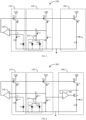
- FIG. 3 illustrates a schematic diagram of yet another exemplary apparatus 300 for generating a temperature-compensated reference voltage V REF in accordance with the present invention.
- the concept behind the apparatus 300 stems from the fact that resistors may be made more consistent than FETs; and thus, better matching between the resistors may be achieved as compared to FETs. Accordingly, the concept behind apparatus 300 is to replace the current sources M1, M2, and M3 with respective resistors R1, R2, and R3 (having substantially equal resistance) and apply negative feedback control using Op Amps 130 and 245 to impress substantially the same voltages across the resistors R1, R2, and R3. This ensures that the currents I1, I2, and I3 generated respectively through the resistors R1, R2, and R3 are substantially the same, which leads to significant reduction in error in the reference voltage V REF .
- the apparatus 300 includes a sub-circuit 310 configured to generate a I CTAT current, a sub-circuit 320 configured to generate a I PTAT current, and a sub-circuit 340 configured to generate a temperature-compensated reference voltage V REF .
- the sub-circuits 310, 320, and 340 are respectively similar to sub-circuits 110, 120, and 240 of apparatus 200, but differ in that resistors R1, R2, and R3 are substituted for the current source FETs M1, M2, and M3, respectively.
- the apparatus 300 further includes a FET M10, which may be implemented with a PMOS FET, coupled between the supply voltage rail Vdd and the resistors R1, R2, and R3.
- the output of the Op Amp 130 is coupled to the gate of FET M10 to control a voltage V SB at a node common to resistors R1, R2, and R3. This is called single-point biasing, where the negative feedback operates on a bias voltage (e.g., V SB ) at a single node.
- V SB bias voltage
- the negative feedback control provided by Op Amp 130 forces the voltage V A and V B to be substantially the same.
- the negative feedback control produced by Op Amp 245 forces the voltages V B and Vc to be substantially the same.
- the resistors R1, R2, and R3 Since the voltages across the resistors R1, R2, and R3 are substantially the same, and the resistors R1, R2, and R3 may be fabricated to have substantially the same resistance, the temperature-compensated currents I1, I2, and I3 are substantially the same. This results in a significant reduction in the error in generating the reference voltage V REF .
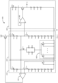
- FIG. 4 illustrates a schematic diagram of still another exemplary apparatus 400 for generating a temperature-compensated reference voltage V REF in accordance with the present invention.
- the apparatus 400 may be an example of a more detailed implementation of reference voltage source 300.
- the apparatus 400 includes a sub-circuit 410 configured to generate a I CTAT current, a sub-circuit 420 configured to generate a I PTAT current, and a sub-circuit 440 configured to generate a temperature-compensated reference voltage V REF .
- the sub-circuits 410, 420, and 440 are similar to sub-circuits 310, 320, and 340 of apparatus 300, respectively.
- the remaining circuitry of apparatus 400 namely Op Amps 130 and 245 and FET M10, are substantially the same as that of apparatus 300.
- resistor R1 is replaced by series-coupled resistors R11 and R12;
- resistor R2 is replaced by series-coupled resistors R21 and R22;
- resistor R3 is replaced by series-coupled resistors R31 and R32;
- resistor R4 is replaced by series-coupled resistors R41-R48;
- resistor R5 is replaced by a pair of series-coupled resistors R51-R52 and R53-R54 coupled in parallel with each other;
- resistor R6 is replaced by series-coupled resistors R61-R68;
- resistor R7 is replaced by series-coupled resistors R71-R74;
- diode D1 is replaced with diode-connected bipolar transistor Q1; and
- diode bank 125 of parallel diodes D21-D2N is replaced by a diode bank 425 of parallel diode-connected bipolar transistors Q21-Q2N.
- apparatus 400 The principle of operation of apparatus 400 is essentially the same as that of apparatus 300.
- the reasons for multiple resistors in apparatus 400 in place of single resistors in apparatus 300 are two folds: (1) Due to process requirements (e.g., limitations on the length-to-width ratio of a resistor), multiple resistors (each compliant with the process requirement) may need to be connected in series or in parallel to achieve the desired resistance; and (2) multiple resistors allow for process variations to be statistically averaged out for better control of the total resistance of each set of resistors. Note that the number and/or combination of resistors that replace each single resistor may vary in other implementations. It should be apparent to one of skill in the art that the concept disclosed herein is not limited to the particular implementation illustrated in FIG. 4 .
- FIG. 5 illustrates a flow diagram of an exemplary method 500 for generating a temperature-compensated reference voltage V REF in accordance with another aspect of the disclosure, not covered by the claims.
- the method 500 includes generating a first temperature-compensated current through a first set of one or more resistors, wherein a first voltage is generated across the first set of one or more resistors based on the first temperature-compensated current (block 502).
- examples of means for generating a first temperature-compensated current I2 include the circuitry having: (1) resistor(s) R1 (or R11-R12), R2 (or R21-R22), R4 (or R41-R48), R5 (or R51-R54), and R6 (or R61-R68); (2) diode D1 or diode-connected transistor Q1; (3) diode bank 125 of diodes D21-D2N coupled in parallel or diode bank 425 of diode-connected transistors Q21-Q2N; and (4) control circuit including Op Amp 130 and transistor (e.g., FET) M10.
- the first temperature-compensated current I2 flows through a first set of one or more resistor(s) R2 or R21-R22, wherein a first voltage (V SB -V B ) is generated across the first set of one or more resistor(s) R2 or R21-R22 based on the first temperature-compensated current I2.
- the method 500 includes generating a second voltage across a second set of one or more resistors, wherein the second voltage is based on the first voltage, and wherein a second temperature-compensated current is generated through the second set of resistors based on the second voltage (block 504).
- examples of means for generating a second voltage include Op Amp 245 and transistor (e.g., FET) M4.
- the second voltage (V SB -V C ) is generated across the second set of one or more resistor(s) R3 or R31-R32, wherein the second voltage (V SB -V C ) is based (e.g., substantially equal to) the first voltage (V SB -V B ), and wherein the second temperature-compensated current I3 is generated through the second set of resistor(s) R3 or R31-R32 based on the second voltage (V SB -V C ).
- the method 500 includes applying the second current through a third set of one or more resistors, wherein a temperature-compensated reference voltage is generated across the third set of one or more resistors (block 506).
- examples of means for applying the second current through a third set of one or more resistors include the series-connection of the resistor R3 or R31-R32, FET M4, and resistor(s) R7 or R71-R74.
- the second current I3 is applied through the third set of one or more resistor(s) R7 or R71-R74 to generate a temperature-compensated reference voltage V REF across the third set of one or more resistor(s) R7 or R71-R74.
Landscapes
- Engineering & Computer Science (AREA)
- Physics & Mathematics (AREA)
- Microelectronics & Electronic Packaging (AREA)
- Nonlinear Science (AREA)
- Electromagnetism (AREA)
- General Physics & Mathematics (AREA)
- Radar, Positioning & Navigation (AREA)
- Automation & Control Theory (AREA)
- Power Engineering (AREA)
- Control Of Electrical Variables (AREA)
- Dc-Dc Converters (AREA)
Applications Claiming Priority (2)
| Application Number | Priority Date | Filing Date | Title |
|---|---|---|---|
| US14/970,265 US9898029B2 (en) | 2015-12-15 | 2015-12-15 | Temperature-compensated reference voltage generator that impresses controlled voltages across resistors |
| PCT/US2016/063139 WO2017105796A1 (en) | 2015-12-15 | 2016-11-21 | Temperature-compensated reference voltage generator that impresses controlled voltages across resistors |
Publications (2)
| Publication Number | Publication Date |
|---|---|
| EP3391171A1 EP3391171A1 (en) | 2018-10-24 |
| EP3391171B1 true EP3391171B1 (en) | 2024-02-14 |
Family
ID=57544532
Family Applications (1)
| Application Number | Title | Priority Date | Filing Date |
|---|---|---|---|
| EP16810538.5A Active EP3391171B1 (en) | 2015-12-15 | 2016-11-21 | Temperature-compensated reference voltage generator that impresses controlled voltages across resistors |
Country Status (9)
| Country | Link |
|---|---|
| US (1) | US9898029B2 (enExample) |
| EP (1) | EP3391171B1 (enExample) |
| JP (1) | JP6800979B2 (enExample) |
| KR (1) | KR102579232B1 (enExample) |
| CN (1) | CN108369428B (enExample) |
| BR (1) | BR112018011919A2 (enExample) |
| CA (1) | CA3003912A1 (enExample) |
| TW (1) | TWI643049B (enExample) |
| WO (1) | WO2017105796A1 (enExample) |
Families Citing this family (11)
| Publication number | Priority date | Publication date | Assignee | Title |
|---|---|---|---|---|
| US10222817B1 (en) * | 2017-09-29 | 2019-03-05 | Cavium, Llc | Method and circuit for low voltage current-mode bandgap |
| TWI651609B (zh) * | 2017-02-09 | 2019-02-21 | 新唐科技股份有限公司 | 低電壓鎖定電路及其整合參考電壓產生電路之裝置 |
| CN109617410B (zh) * | 2018-12-28 | 2024-01-19 | 中国电子科技集团公司第五十八研究所 | 一种新型浮动电压检测电路 |
| CN112034920B (zh) * | 2019-06-04 | 2022-06-17 | 极创电子股份有限公司 | 电压产生器 |
| US11127437B2 (en) * | 2019-10-01 | 2021-09-21 | Macronix International Co., Ltd. | Managing startups of bandgap reference circuits in memory systems |
| EP3812873B1 (en) * | 2019-10-24 | 2025-02-26 | NXP USA, Inc. | Voltage reference generation with compensation for temperature variation |
| US11233513B2 (en) * | 2019-11-05 | 2022-01-25 | Mediatek Inc. | Reference voltage buffer with settling enhancement |
| TWI792977B (zh) * | 2022-04-11 | 2023-02-11 | 立錡科技股份有限公司 | 具有高次溫度補償功能的參考訊號產生電路 |
| US11815927B1 (en) * | 2022-05-19 | 2023-11-14 | Changxin Memory Technologies, Inc. | Bandgap reference circuit and chip |
| US20240393819A1 (en) * | 2023-05-25 | 2024-11-28 | Silicon Laboratories Inc. | Voltage and current reference circuits |
| US12267071B2 (en) * | 2023-06-01 | 2025-04-01 | Allegro Microsystems, Llc | Desaturation circuit having temperature compensation |
Family Cites Families (18)
| Publication number | Priority date | Publication date | Assignee | Title |
|---|---|---|---|---|
| JPS6017316A (ja) * | 1983-07-08 | 1985-01-29 | Canon Inc | 温度補償回路 |
| JP3586073B2 (ja) * | 1997-07-29 | 2004-11-10 | 株式会社東芝 | 基準電圧発生回路 |
| US6891358B2 (en) | 2002-12-27 | 2005-05-10 | Analog Devices, Inc. | Bandgap voltage reference circuit with high power supply rejection ratio (PSRR) and curvature correction |
| US7119528B1 (en) * | 2005-04-26 | 2006-10-10 | International Business Machines Corporation | Low voltage bandgap reference with power supply rejection |
| US7636010B2 (en) * | 2007-09-03 | 2009-12-22 | Elite Semiconductor Memory Technology Inc. | Process independent curvature compensation scheme for bandgap reference |
| US7612606B2 (en) | 2007-12-21 | 2009-11-03 | Analog Devices, Inc. | Low voltage current and voltage generator |
| US7750728B2 (en) | 2008-03-25 | 2010-07-06 | Analog Devices, Inc. | Reference voltage circuit |
| TWI377461B (en) * | 2008-05-15 | 2012-11-21 | Pixart Imaging Inc | Reference voltage adjustment circuits for temperature compensation and related transmitter devices |
| CN101923366B (zh) | 2009-06-17 | 2012-10-03 | 中国科学院微电子研究所 | 带熔丝校准的cmos带隙基准电压源 |
| CN101630176B (zh) * | 2009-07-28 | 2011-11-16 | 中国科学院微电子研究所 | 低电压cmos带隙基准电压源 |
| CN102236359B (zh) * | 2010-02-22 | 2015-07-29 | 塞瑞斯逻辑公司 | 不随电源变化的带隙参考系统 |
| US8536854B2 (en) | 2010-09-30 | 2013-09-17 | Cirrus Logic, Inc. | Supply invariant bandgap reference system |
| TWI400884B (zh) * | 2010-05-28 | 2013-07-01 | Macronix Int Co Ltd | 時鐘積體電路 |
| TWI473433B (zh) * | 2011-10-21 | 2015-02-11 | Macronix Int Co Ltd | 時鐘積體電路 |
| US8941369B2 (en) | 2012-03-19 | 2015-01-27 | Sandisk Technologies Inc. | Curvature compensated band-gap design trimmable at a single temperature |
| US8937468B2 (en) * | 2012-08-13 | 2015-01-20 | Northrop Grumman Systems Corporation | Power supply systems and methods |
| TWI521326B (zh) * | 2013-12-27 | 2016-02-11 | 慧榮科技股份有限公司 | 帶隙參考電壓產生電路 |
| EP2897021B1 (en) * | 2014-01-21 | 2020-04-29 | Dialog Semiconductor (UK) Limited | An apparatus and method for a low voltage reference and oscillator |
-
2015
- 2015-12-15 US US14/970,265 patent/US9898029B2/en active Active
-
2016
- 2016-11-21 BR BR112018011919A patent/BR112018011919A2/pt not_active Application Discontinuation
- 2016-11-21 CA CA3003912A patent/CA3003912A1/en not_active Abandoned
- 2016-11-21 KR KR1020187016551A patent/KR102579232B1/ko active Active
- 2016-11-21 CN CN201680072887.2A patent/CN108369428B/zh active Active
- 2016-11-21 TW TW105138039A patent/TWI643049B/zh not_active IP Right Cessation
- 2016-11-21 WO PCT/US2016/063139 patent/WO2017105796A1/en not_active Ceased
- 2016-11-21 EP EP16810538.5A patent/EP3391171B1/en active Active
- 2016-11-21 JP JP2018530836A patent/JP6800979B2/ja active Active
Also Published As
| Publication number | Publication date |
|---|---|
| US9898029B2 (en) | 2018-02-20 |
| WO2017105796A1 (en) | 2017-06-22 |
| CA3003912A1 (en) | 2017-06-22 |
| JP6800979B2 (ja) | 2020-12-16 |
| BR112018011919A2 (pt) | 2018-11-27 |
| TWI643049B (zh) | 2018-12-01 |
| KR102579232B1 (ko) | 2023-09-14 |
| TW201725468A (zh) | 2017-07-16 |
| JP2018537789A (ja) | 2018-12-20 |
| US20170168518A1 (en) | 2017-06-15 |
| CN108369428B (zh) | 2020-01-14 |
| KR20180095523A (ko) | 2018-08-27 |
| CN108369428A (zh) | 2018-08-03 |
| EP3391171A1 (en) | 2018-10-24 |
Similar Documents
| Publication | Publication Date | Title |
|---|---|---|
| EP3391171B1 (en) | Temperature-compensated reference voltage generator that impresses controlled voltages across resistors | |
| US11775001B2 (en) | Sub-bandgap compensated reference voltage generation circuit | |
| CN107608444B (zh) | 基准电压发生器电路和电子系统 | |
| US6563371B2 (en) | Current bandgap voltage reference circuits and related methods | |
| JP3519958B2 (ja) | 基準電圧発生回路 | |
| US9298202B2 (en) | Device for generating an adjustable bandgap reference voltage with large power supply rejection rate | |
| US9092044B2 (en) | Low voltage, low power bandgap circuit | |
| CN108536207B (zh) | 电流产生电路和包括其的带隙基准电路及半导体器件 | |
| TW201533559A (zh) | 電壓參考電路 | |
| US20160274617A1 (en) | Bandgap circuit | |
| TW202020596A (zh) | 提供可調恆定電流之電流電路 | |
| CN114341764B (zh) | 集成电路 | |
| TW201931046A (zh) | 包括帶隙參考電路的電路 | |
| US9600013B1 (en) | Bandgap reference circuit | |
| US20120242317A1 (en) | Reference voltage circuit | |
| US9952617B1 (en) | Reference current circuit architecture | |
| US10503197B2 (en) | Current generation circuit | |
| JP6413005B2 (ja) | 半導体装置及び電子システム | |
| US10310539B2 (en) | Proportional to absolute temperature reference circuit and a voltage reference circuit | |
| JP2005044051A (ja) | 基準電圧発生回路 | |
| US10338616B2 (en) | Reference generation circuit | |
| US20130328621A1 (en) | Semiconductor integrated circuit | |
| KR101603707B1 (ko) | 밴드갭 기준 전압 발생 회로 | |
| CN120523275A (zh) | 混合偏置电路及其相关产品 | |
| WO2004042782A2 (en) | Apparatus and method for implementing a constant transconductance circuit |
Legal Events
| Date | Code | Title | Description |
|---|---|---|---|
| STAA | Information on the status of an ep patent application or granted ep patent |
Free format text: STATUS: UNKNOWN |
|
| STAA | Information on the status of an ep patent application or granted ep patent |
Free format text: STATUS: THE INTERNATIONAL PUBLICATION HAS BEEN MADE |
|
| PUAI | Public reference made under article 153(3) epc to a published international application that has entered the european phase |
Free format text: ORIGINAL CODE: 0009012 |
|
| STAA | Information on the status of an ep patent application or granted ep patent |
Free format text: STATUS: REQUEST FOR EXAMINATION WAS MADE |
|
| 17P | Request for examination filed |
Effective date: 20180508 |
|
| AK | Designated contracting states |
Kind code of ref document: A1 Designated state(s): AL AT BE BG CH CY CZ DE DK EE ES FI FR GB GR HR HU IE IS IT LI LT LU LV MC MK MT NL NO PL PT RO RS SE SI SK SM TR |
|
| AX | Request for extension of the european patent |
Extension state: BA ME |
|
| DAV | Request for validation of the european patent (deleted) | ||
| DAX | Request for extension of the european patent (deleted) | ||
| STAA | Information on the status of an ep patent application or granted ep patent |
Free format text: STATUS: EXAMINATION IS IN PROGRESS |
|
| 17Q | First examination report despatched |
Effective date: 20190506 |
|
| RIC1 | Information provided on ipc code assigned before grant |
Ipc: G05F 3/26 20060101ALI20230725BHEP Ipc: G05F 3/24 20060101ALI20230725BHEP Ipc: G05F 3/22 20060101ALI20230725BHEP Ipc: G05F 3/30 20060101AFI20230725BHEP |
|
| GRAP | Despatch of communication of intention to grant a patent |
Free format text: ORIGINAL CODE: EPIDOSNIGR1 |
|
| STAA | Information on the status of an ep patent application or granted ep patent |
Free format text: STATUS: GRANT OF PATENT IS INTENDED |
|
| INTG | Intention to grant announced |
Effective date: 20230905 |
|
| GRAS | Grant fee paid |
Free format text: ORIGINAL CODE: EPIDOSNIGR3 |
|
| GRAA | (expected) grant |
Free format text: ORIGINAL CODE: 0009210 |
|
| STAA | Information on the status of an ep patent application or granted ep patent |
Free format text: STATUS: THE PATENT HAS BEEN GRANTED |
|
| AK | Designated contracting states |
Kind code of ref document: B1 Designated state(s): AL AT BE BG CH CY CZ DE DK EE ES FI FR GB GR HR HU IE IS IT LI LT LU LV MC MK MT NL NO PL PT RO RS SE SI SK SM TR |
|
| REG | Reference to a national code |
Ref country code: GB Ref legal event code: FG4D |
|
| REG | Reference to a national code |
Ref country code: CH Ref legal event code: EP |
|
| REG | Reference to a national code |
Ref country code: DE Ref legal event code: R096 Ref document number: 602016085794 Country of ref document: DE |
|
| REG | Reference to a national code |
Ref country code: IE Ref legal event code: FG4D |
|
| REG | Reference to a national code |
Ref country code: LT Ref legal event code: MG9D |
|
| REG | Reference to a national code |
Ref country code: NL Ref legal event code: MP Effective date: 20240214 |
|
| PG25 | Lapsed in a contracting state [announced via postgrant information from national office to epo] |
Ref country code: IS Free format text: LAPSE BECAUSE OF FAILURE TO SUBMIT A TRANSLATION OF THE DESCRIPTION OR TO PAY THE FEE WITHIN THE PRESCRIBED TIME-LIMIT Effective date: 20240614 |
|
| PG25 | Lapsed in a contracting state [announced via postgrant information from national office to epo] |
Ref country code: LT Free format text: LAPSE BECAUSE OF FAILURE TO SUBMIT A TRANSLATION OF THE DESCRIPTION OR TO PAY THE FEE WITHIN THE PRESCRIBED TIME-LIMIT Effective date: 20240214 |
|
| PG25 | Lapsed in a contracting state [announced via postgrant information from national office to epo] |
Ref country code: GR Free format text: LAPSE BECAUSE OF FAILURE TO SUBMIT A TRANSLATION OF THE DESCRIPTION OR TO PAY THE FEE WITHIN THE PRESCRIBED TIME-LIMIT Effective date: 20240515 |
|
| REG | Reference to a national code |
Ref country code: AT Ref legal event code: MK05 Ref document number: 1657571 Country of ref document: AT Kind code of ref document: T Effective date: 20240214 |
|
| PG25 | Lapsed in a contracting state [announced via postgrant information from national office to epo] |
Ref country code: RS Free format text: LAPSE BECAUSE OF FAILURE TO SUBMIT A TRANSLATION OF THE DESCRIPTION OR TO PAY THE FEE WITHIN THE PRESCRIBED TIME-LIMIT Effective date: 20240514 Ref country code: HR Free format text: LAPSE BECAUSE OF FAILURE TO SUBMIT A TRANSLATION OF THE DESCRIPTION OR TO PAY THE FEE WITHIN THE PRESCRIBED TIME-LIMIT Effective date: 20240214 Ref country code: NL Free format text: LAPSE BECAUSE OF FAILURE TO SUBMIT A TRANSLATION OF THE DESCRIPTION OR TO PAY THE FEE WITHIN THE PRESCRIBED TIME-LIMIT Effective date: 20240214 |
|
| PG25 | Lapsed in a contracting state [announced via postgrant information from national office to epo] |
Ref country code: ES Free format text: LAPSE BECAUSE OF FAILURE TO SUBMIT A TRANSLATION OF THE DESCRIPTION OR TO PAY THE FEE WITHIN THE PRESCRIBED TIME-LIMIT Effective date: 20240214 |
|
| PG25 | Lapsed in a contracting state [announced via postgrant information from national office to epo] |
Ref country code: AT Free format text: LAPSE BECAUSE OF FAILURE TO SUBMIT A TRANSLATION OF THE DESCRIPTION OR TO PAY THE FEE WITHIN THE PRESCRIBED TIME-LIMIT Effective date: 20240214 |
|
| PG25 | Lapsed in a contracting state [announced via postgrant information from national office to epo] |
Ref country code: RS Free format text: LAPSE BECAUSE OF FAILURE TO SUBMIT A TRANSLATION OF THE DESCRIPTION OR TO PAY THE FEE WITHIN THE PRESCRIBED TIME-LIMIT Effective date: 20240514 Ref country code: NO Free format text: LAPSE BECAUSE OF FAILURE TO SUBMIT A TRANSLATION OF THE DESCRIPTION OR TO PAY THE FEE WITHIN THE PRESCRIBED TIME-LIMIT Effective date: 20240514 Ref country code: NL Free format text: LAPSE BECAUSE OF FAILURE TO SUBMIT A TRANSLATION OF THE DESCRIPTION OR TO PAY THE FEE WITHIN THE PRESCRIBED TIME-LIMIT Effective date: 20240214 Ref country code: LT Free format text: LAPSE BECAUSE OF FAILURE TO SUBMIT A TRANSLATION OF THE DESCRIPTION OR TO PAY THE FEE WITHIN THE PRESCRIBED TIME-LIMIT Effective date: 20240214 Ref country code: IS Free format text: LAPSE BECAUSE OF FAILURE TO SUBMIT A TRANSLATION OF THE DESCRIPTION OR TO PAY THE FEE WITHIN THE PRESCRIBED TIME-LIMIT Effective date: 20240614 Ref country code: HR Free format text: LAPSE BECAUSE OF FAILURE TO SUBMIT A TRANSLATION OF THE DESCRIPTION OR TO PAY THE FEE WITHIN THE PRESCRIBED TIME-LIMIT Effective date: 20240214 Ref country code: GR Free format text: LAPSE BECAUSE OF FAILURE TO SUBMIT A TRANSLATION OF THE DESCRIPTION OR TO PAY THE FEE WITHIN THE PRESCRIBED TIME-LIMIT Effective date: 20240515 Ref country code: FI Free format text: LAPSE BECAUSE OF FAILURE TO SUBMIT A TRANSLATION OF THE DESCRIPTION OR TO PAY THE FEE WITHIN THE PRESCRIBED TIME-LIMIT Effective date: 20240214 Ref country code: ES Free format text: LAPSE BECAUSE OF FAILURE TO SUBMIT A TRANSLATION OF THE DESCRIPTION OR TO PAY THE FEE WITHIN THE PRESCRIBED TIME-LIMIT Effective date: 20240214 Ref country code: BG Free format text: LAPSE BECAUSE OF FAILURE TO SUBMIT A TRANSLATION OF THE DESCRIPTION OR TO PAY THE FEE WITHIN THE PRESCRIBED TIME-LIMIT Effective date: 20240214 Ref country code: AT Free format text: LAPSE BECAUSE OF FAILURE TO SUBMIT A TRANSLATION OF THE DESCRIPTION OR TO PAY THE FEE WITHIN THE PRESCRIBED TIME-LIMIT Effective date: 20240214 |
|
| PG25 | Lapsed in a contracting state [announced via postgrant information from national office to epo] |
Ref country code: PT Free format text: LAPSE BECAUSE OF FAILURE TO SUBMIT A TRANSLATION OF THE DESCRIPTION OR TO PAY THE FEE WITHIN THE PRESCRIBED TIME-LIMIT Effective date: 20240614 Ref country code: PL Free format text: LAPSE BECAUSE OF FAILURE TO SUBMIT A TRANSLATION OF THE DESCRIPTION OR TO PAY THE FEE WITHIN THE PRESCRIBED TIME-LIMIT Effective date: 20240214 |
|
| PG25 | Lapsed in a contracting state [announced via postgrant information from national office to epo] |
Ref country code: SE Free format text: LAPSE BECAUSE OF FAILURE TO SUBMIT A TRANSLATION OF THE DESCRIPTION OR TO PAY THE FEE WITHIN THE PRESCRIBED TIME-LIMIT Effective date: 20240214 Ref country code: PT Free format text: LAPSE BECAUSE OF FAILURE TO SUBMIT A TRANSLATION OF THE DESCRIPTION OR TO PAY THE FEE WITHIN THE PRESCRIBED TIME-LIMIT Effective date: 20240614 Ref country code: PL Free format text: LAPSE BECAUSE OF FAILURE TO SUBMIT A TRANSLATION OF THE DESCRIPTION OR TO PAY THE FEE WITHIN THE PRESCRIBED TIME-LIMIT Effective date: 20240214 Ref country code: LV Free format text: LAPSE BECAUSE OF FAILURE TO SUBMIT A TRANSLATION OF THE DESCRIPTION OR TO PAY THE FEE WITHIN THE PRESCRIBED TIME-LIMIT Effective date: 20240214 |
|
| PG25 | Lapsed in a contracting state [announced via postgrant information from national office to epo] |
Ref country code: DK Free format text: LAPSE BECAUSE OF FAILURE TO SUBMIT A TRANSLATION OF THE DESCRIPTION OR TO PAY THE FEE WITHIN THE PRESCRIBED TIME-LIMIT Effective date: 20240214 |
|
| PG25 | Lapsed in a contracting state [announced via postgrant information from national office to epo] |
Ref country code: SM Free format text: LAPSE BECAUSE OF FAILURE TO SUBMIT A TRANSLATION OF THE DESCRIPTION OR TO PAY THE FEE WITHIN THE PRESCRIBED TIME-LIMIT Effective date: 20240214 |
|
| PG25 | Lapsed in a contracting state [announced via postgrant information from national office to epo] |
Ref country code: CZ Free format text: LAPSE BECAUSE OF FAILURE TO SUBMIT A TRANSLATION OF THE DESCRIPTION OR TO PAY THE FEE WITHIN THE PRESCRIBED TIME-LIMIT Effective date: 20240214 Ref country code: EE Free format text: LAPSE BECAUSE OF FAILURE TO SUBMIT A TRANSLATION OF THE DESCRIPTION OR TO PAY THE FEE WITHIN THE PRESCRIBED TIME-LIMIT Effective date: 20240214 |
|
| PG25 | Lapsed in a contracting state [announced via postgrant information from national office to epo] |
Ref country code: SK Free format text: LAPSE BECAUSE OF FAILURE TO SUBMIT A TRANSLATION OF THE DESCRIPTION OR TO PAY THE FEE WITHIN THE PRESCRIBED TIME-LIMIT Effective date: 20240214 |
|
| PG25 | Lapsed in a contracting state [announced via postgrant information from national office to epo] |
Ref country code: SM Free format text: LAPSE BECAUSE OF FAILURE TO SUBMIT A TRANSLATION OF THE DESCRIPTION OR TO PAY THE FEE WITHIN THE PRESCRIBED TIME-LIMIT Effective date: 20240214 Ref country code: SK Free format text: LAPSE BECAUSE OF FAILURE TO SUBMIT A TRANSLATION OF THE DESCRIPTION OR TO PAY THE FEE WITHIN THE PRESCRIBED TIME-LIMIT Effective date: 20240214 Ref country code: RO Free format text: LAPSE BECAUSE OF FAILURE TO SUBMIT A TRANSLATION OF THE DESCRIPTION OR TO PAY THE FEE WITHIN THE PRESCRIBED TIME-LIMIT Effective date: 20240214 Ref country code: EE Free format text: LAPSE BECAUSE OF FAILURE TO SUBMIT A TRANSLATION OF THE DESCRIPTION OR TO PAY THE FEE WITHIN THE PRESCRIBED TIME-LIMIT Effective date: 20240214 Ref country code: DK Free format text: LAPSE BECAUSE OF FAILURE TO SUBMIT A TRANSLATION OF THE DESCRIPTION OR TO PAY THE FEE WITHIN THE PRESCRIBED TIME-LIMIT Effective date: 20240214 Ref country code: CZ Free format text: LAPSE BECAUSE OF FAILURE TO SUBMIT A TRANSLATION OF THE DESCRIPTION OR TO PAY THE FEE WITHIN THE PRESCRIBED TIME-LIMIT Effective date: 20240214 |
|
| REG | Reference to a national code |
Ref country code: DE Ref legal event code: R097 Ref document number: 602016085794 Country of ref document: DE |
|
| PG25 | Lapsed in a contracting state [announced via postgrant information from national office to epo] |
Ref country code: IT Free format text: LAPSE BECAUSE OF FAILURE TO SUBMIT A TRANSLATION OF THE DESCRIPTION OR TO PAY THE FEE WITHIN THE PRESCRIBED TIME-LIMIT Effective date: 20240214 |
|
| PLBE | No opposition filed within time limit |
Free format text: ORIGINAL CODE: 0009261 |
|
| STAA | Information on the status of an ep patent application or granted ep patent |
Free format text: STATUS: NO OPPOSITION FILED WITHIN TIME LIMIT |
|
| PG25 | Lapsed in a contracting state [announced via postgrant information from national office to epo] |
Ref country code: IT Free format text: LAPSE BECAUSE OF FAILURE TO SUBMIT A TRANSLATION OF THE DESCRIPTION OR TO PAY THE FEE WITHIN THE PRESCRIBED TIME-LIMIT Effective date: 20240214 |
|
| PGFP | Annual fee paid to national office [announced via postgrant information from national office to epo] |
Ref country code: DE Payment date: 20241010 Year of fee payment: 9 |
|
| PGFP | Annual fee paid to national office [announced via postgrant information from national office to epo] |
Ref country code: GB Payment date: 20241010 Year of fee payment: 9 |
|
| 26N | No opposition filed |
Effective date: 20241115 |
|
| PGFP | Annual fee paid to national office [announced via postgrant information from national office to epo] |
Ref country code: FR Payment date: 20241010 Year of fee payment: 9 |
|
| PG25 | Lapsed in a contracting state [announced via postgrant information from national office to epo] |
Ref country code: SI Free format text: LAPSE BECAUSE OF FAILURE TO SUBMIT A TRANSLATION OF THE DESCRIPTION OR TO PAY THE FEE WITHIN THE PRESCRIBED TIME-LIMIT Effective date: 20240214 |
|
| REG | Reference to a national code |
Ref country code: CH Ref legal event code: PL |
|
| PG25 | Lapsed in a contracting state [announced via postgrant information from national office to epo] |
Ref country code: MC Free format text: LAPSE BECAUSE OF FAILURE TO SUBMIT A TRANSLATION OF THE DESCRIPTION OR TO PAY THE FEE WITHIN THE PRESCRIBED TIME-LIMIT Effective date: 20240214 |
|
| PG25 | Lapsed in a contracting state [announced via postgrant information from national office to epo] |
Ref country code: LU Free format text: LAPSE BECAUSE OF NON-PAYMENT OF DUE FEES Effective date: 20241121 |
|
| REG | Reference to a national code |
Ref country code: CH Ref legal event code: PL |
|
| PG25 | Lapsed in a contracting state [announced via postgrant information from national office to epo] |
Ref country code: CH Free format text: LAPSE BECAUSE OF NON-PAYMENT OF DUE FEES Effective date: 20241130 |
|
| REG | Reference to a national code |
Ref country code: BE Ref legal event code: MM Effective date: 20241130 |
|
| PG25 | Lapsed in a contracting state [announced via postgrant information from national office to epo] |
Ref country code: BE Free format text: LAPSE BECAUSE OF NON-PAYMENT OF DUE FEES Effective date: 20241130 |
|
| PG25 | Lapsed in a contracting state [announced via postgrant information from national office to epo] |
Ref country code: IE Free format text: LAPSE BECAUSE OF NON-PAYMENT OF DUE FEES Effective date: 20241121 |