EP3389174A1 - Stromwandlungsvorrichtung - Google Patents
Stromwandlungsvorrichtung Download PDFInfo
- Publication number
- EP3389174A1 EP3389174A1 EP18176497.8A EP18176497A EP3389174A1 EP 3389174 A1 EP3389174 A1 EP 3389174A1 EP 18176497 A EP18176497 A EP 18176497A EP 3389174 A1 EP3389174 A1 EP 3389174A1
- Authority
- EP
- European Patent Office
- Prior art keywords
- voltage
- phase
- bus
- converter
- control unit
- Prior art date
- Legal status (The legal status is an assumption and is not a legal conclusion. Google has not performed a legal analysis and makes no representation as to the accuracy of the status listed.)
- Ceased
Links
Images


Classifications
-
- H—ELECTRICITY
- H02—GENERATION; CONVERSION OR DISTRIBUTION OF ELECTRIC POWER
- H02M—APPARATUS FOR CONVERSION BETWEEN AC AND AC, BETWEEN AC AND DC, OR BETWEEN DC AND DC, AND FOR USE WITH MAINS OR SIMILAR POWER SUPPLY SYSTEMS; CONVERSION OF DC OR AC INPUT POWER INTO SURGE OUTPUT POWER; CONTROL OR REGULATION THEREOF
- H02M7/00—Conversion of ac power input into dc power output; Conversion of dc power input into ac power output
- H02M7/42—Conversion of dc power input into ac power output without possibility of reversal
- H02M7/44—Conversion of dc power input into ac power output without possibility of reversal by static converters
- H02M7/48—Conversion of dc power input into ac power output without possibility of reversal by static converters using discharge tubes with control electrode or semiconductor devices with control electrode
- H02M7/483—Converters with outputs that each can have more than two voltages levels
- H02M7/4833—Capacitor voltage balancing
-
- H—ELECTRICITY
- H02—GENERATION; CONVERSION OR DISTRIBUTION OF ELECTRIC POWER
- H02M—APPARATUS FOR CONVERSION BETWEEN AC AND AC, BETWEEN AC AND DC, OR BETWEEN DC AND DC, AND FOR USE WITH MAINS OR SIMILAR POWER SUPPLY SYSTEMS; CONVERSION OF DC OR AC INPUT POWER INTO SURGE OUTPUT POWER; CONTROL OR REGULATION THEREOF
- H02M5/00—Conversion of ac power input into ac power output, e.g. for change of voltage, for change of frequency, for change of number of phases
- H02M5/02—Conversion of ac power input into ac power output, e.g. for change of voltage, for change of frequency, for change of number of phases without intermediate conversion into dc
- H02M5/04—Conversion of ac power input into ac power output, e.g. for change of voltage, for change of frequency, for change of number of phases without intermediate conversion into dc by static converters
- H02M5/22—Conversion of ac power input into ac power output, e.g. for change of voltage, for change of frequency, for change of number of phases without intermediate conversion into dc by static converters using discharge tubes with control electrode or semiconductor devices with control electrode
- H02M5/275—Conversion of ac power input into ac power output, e.g. for change of voltage, for change of frequency, for change of number of phases without intermediate conversion into dc by static converters using discharge tubes with control electrode or semiconductor devices with control electrode using devices of a triode or transistor type requiring continuous application of a control signal
- H02M5/293—Conversion of ac power input into ac power output, e.g. for change of voltage, for change of frequency, for change of number of phases without intermediate conversion into dc by static converters using discharge tubes with control electrode or semiconductor devices with control electrode using devices of a triode or transistor type requiring continuous application of a control signal using semiconductor devices only
-
- H—ELECTRICITY
- H02—GENERATION; CONVERSION OR DISTRIBUTION OF ELECTRIC POWER
- H02M—APPARATUS FOR CONVERSION BETWEEN AC AND AC, BETWEEN AC AND DC, OR BETWEEN DC AND DC, AND FOR USE WITH MAINS OR SIMILAR POWER SUPPLY SYSTEMS; CONVERSION OF DC OR AC INPUT POWER INTO SURGE OUTPUT POWER; CONTROL OR REGULATION THEREOF
- H02M5/00—Conversion of ac power input into ac power output, e.g. for change of voltage, for change of frequency, for change of number of phases
- H02M5/40—Conversion of ac power input into ac power output, e.g. for change of voltage, for change of frequency, for change of number of phases with intermediate conversion into dc
- H02M5/42—Conversion of ac power input into ac power output, e.g. for change of voltage, for change of frequency, for change of number of phases with intermediate conversion into dc by static converters
- H02M5/44—Conversion of ac power input into ac power output, e.g. for change of voltage, for change of frequency, for change of number of phases with intermediate conversion into dc by static converters using discharge tubes or semiconductor devices to convert the intermediate dc into ac
- H02M5/453—Conversion of ac power input into ac power output, e.g. for change of voltage, for change of frequency, for change of number of phases with intermediate conversion into dc by static converters using discharge tubes or semiconductor devices to convert the intermediate dc into ac using devices of a triode or transistor type requiring continuous application of a control signal
- H02M5/458—Conversion of ac power input into ac power output, e.g. for change of voltage, for change of frequency, for change of number of phases with intermediate conversion into dc by static converters using discharge tubes or semiconductor devices to convert the intermediate dc into ac using devices of a triode or transistor type requiring continuous application of a control signal using semiconductor devices only
- H02M5/4585—Conversion of ac power input into ac power output, e.g. for change of voltage, for change of frequency, for change of number of phases with intermediate conversion into dc by static converters using discharge tubes or semiconductor devices to convert the intermediate dc into ac using devices of a triode or transistor type requiring continuous application of a control signal using semiconductor devices only having a rectifier with controlled elements
-
- H—ELECTRICITY
- H02—GENERATION; CONVERSION OR DISTRIBUTION OF ELECTRIC POWER
- H02M—APPARATUS FOR CONVERSION BETWEEN AC AND AC, BETWEEN AC AND DC, OR BETWEEN DC AND DC, AND FOR USE WITH MAINS OR SIMILAR POWER SUPPLY SYSTEMS; CONVERSION OF DC OR AC INPUT POWER INTO SURGE OUTPUT POWER; CONTROL OR REGULATION THEREOF
- H02M1/00—Details of apparatus for conversion
- H02M1/12—Arrangements for reducing harmonics from ac input or output
-
- H—ELECTRICITY
- H02—GENERATION; CONVERSION OR DISTRIBUTION OF ELECTRIC POWER
- H02M—APPARATUS FOR CONVERSION BETWEEN AC AND AC, BETWEEN AC AND DC, OR BETWEEN DC AND DC, AND FOR USE WITH MAINS OR SIMILAR POWER SUPPLY SYSTEMS; CONVERSION OF DC OR AC INPUT POWER INTO SURGE OUTPUT POWER; CONTROL OR REGULATION THEREOF
- H02M1/00—Details of apparatus for conversion
- H02M1/14—Arrangements for reducing ripples from dc input or output
-
- H—ELECTRICITY
- H02—GENERATION; CONVERSION OR DISTRIBUTION OF ELECTRIC POWER
- H02M—APPARATUS FOR CONVERSION BETWEEN AC AND AC, BETWEEN AC AND DC, OR BETWEEN DC AND DC, AND FOR USE WITH MAINS OR SIMILAR POWER SUPPLY SYSTEMS; CONVERSION OF DC OR AC INPUT POWER INTO SURGE OUTPUT POWER; CONTROL OR REGULATION THEREOF
- H02M5/00—Conversion of ac power input into ac power output, e.g. for change of voltage, for change of frequency, for change of number of phases
- H02M5/40—Conversion of ac power input into ac power output, e.g. for change of voltage, for change of frequency, for change of number of phases with intermediate conversion into dc
- H02M5/42—Conversion of ac power input into ac power output, e.g. for change of voltage, for change of frequency, for change of number of phases with intermediate conversion into dc by static converters
- H02M5/44—Conversion of ac power input into ac power output, e.g. for change of voltage, for change of frequency, for change of number of phases with intermediate conversion into dc by static converters using discharge tubes or semiconductor devices to convert the intermediate dc into ac
- H02M5/453—Conversion of ac power input into ac power output, e.g. for change of voltage, for change of frequency, for change of number of phases with intermediate conversion into dc by static converters using discharge tubes or semiconductor devices to convert the intermediate dc into ac using devices of a triode or transistor type requiring continuous application of a control signal
- H02M5/458—Conversion of ac power input into ac power output, e.g. for change of voltage, for change of frequency, for change of number of phases with intermediate conversion into dc by static converters using discharge tubes or semiconductor devices to convert the intermediate dc into ac using devices of a triode or transistor type requiring continuous application of a control signal using semiconductor devices only
-
- H—ELECTRICITY
- H02—GENERATION; CONVERSION OR DISTRIBUTION OF ELECTRIC POWER
- H02M—APPARATUS FOR CONVERSION BETWEEN AC AND AC, BETWEEN AC AND DC, OR BETWEEN DC AND DC, AND FOR USE WITH MAINS OR SIMILAR POWER SUPPLY SYSTEMS; CONVERSION OF DC OR AC INPUT POWER INTO SURGE OUTPUT POWER; CONTROL OR REGULATION THEREOF
- H02M7/00—Conversion of ac power input into dc power output; Conversion of dc power input into ac power output
- H02M7/42—Conversion of dc power input into ac power output without possibility of reversal
- H02M7/44—Conversion of dc power input into ac power output without possibility of reversal by static converters
- H02M7/48—Conversion of dc power input into ac power output without possibility of reversal by static converters using discharge tubes with control electrode or semiconductor devices with control electrode
- H02M7/483—Converters with outputs that each can have more than two voltages levels
- H02M7/487—Neutral point clamped inverters
-
- H—ELECTRICITY
- H02—GENERATION; CONVERSION OR DISTRIBUTION OF ELECTRIC POWER
- H02M—APPARATUS FOR CONVERSION BETWEEN AC AND AC, BETWEEN AC AND DC, OR BETWEEN DC AND DC, AND FOR USE WITH MAINS OR SIMILAR POWER SUPPLY SYSTEMS; CONVERSION OF DC OR AC INPUT POWER INTO SURGE OUTPUT POWER; CONTROL OR REGULATION THEREOF
- H02M7/00—Conversion of ac power input into dc power output; Conversion of dc power input into ac power output
- H02M7/42—Conversion of dc power input into ac power output without possibility of reversal
- H02M7/44—Conversion of dc power input into ac power output without possibility of reversal by static converters
- H02M7/48—Conversion of dc power input into ac power output without possibility of reversal by static converters using discharge tubes with control electrode or semiconductor devices with control electrode
- H02M7/483—Converters with outputs that each can have more than two voltages levels
- H02M7/49—Combination of the output voltage waveforms of a plurality of converters
-
- H—ELECTRICITY
- H02—GENERATION; CONVERSION OR DISTRIBUTION OF ELECTRIC POWER
- H02M—APPARATUS FOR CONVERSION BETWEEN AC AND AC, BETWEEN AC AND DC, OR BETWEEN DC AND DC, AND FOR USE WITH MAINS OR SIMILAR POWER SUPPLY SYSTEMS; CONVERSION OF DC OR AC INPUT POWER INTO SURGE OUTPUT POWER; CONTROL OR REGULATION THEREOF
- H02M1/00—Details of apparatus for conversion
- H02M1/0095—Hybrid converter topologies, e.g. NPC mixed with flying capacitor, thyristor converter mixed with MMC or charge pump mixed with buck
-
- H—ELECTRICITY
- H02—GENERATION; CONVERSION OR DISTRIBUTION OF ELECTRIC POWER
- H02M—APPARATUS FOR CONVERSION BETWEEN AC AND AC, BETWEEN AC AND DC, OR BETWEEN DC AND DC, AND FOR USE WITH MAINS OR SIMILAR POWER SUPPLY SYSTEMS; CONVERSION OF DC OR AC INPUT POWER INTO SURGE OUTPUT POWER; CONTROL OR REGULATION THEREOF
- H02M7/00—Conversion of ac power input into dc power output; Conversion of dc power input into ac power output
- H02M7/42—Conversion of dc power input into ac power output without possibility of reversal
- H02M7/44—Conversion of dc power input into ac power output without possibility of reversal by static converters
- H02M7/48—Conversion of dc power input into ac power output without possibility of reversal by static converters using discharge tubes with control electrode or semiconductor devices with control electrode
- H02M7/53—Conversion of dc power input into ac power output without possibility of reversal by static converters using discharge tubes with control electrode or semiconductor devices with control electrode using devices of a triode or transistor type requiring continuous application of a control signal
- H02M7/537—Conversion of dc power input into ac power output without possibility of reversal by static converters using discharge tubes with control electrode or semiconductor devices with control electrode using devices of a triode or transistor type requiring continuous application of a control signal using semiconductor devices only, e.g. single switched pulse inverters
- H02M7/539—Conversion of dc power input into ac power output without possibility of reversal by static converters using discharge tubes with control electrode or semiconductor devices with control electrode using devices of a triode or transistor type requiring continuous application of a control signal using semiconductor devices only, e.g. single switched pulse inverters with automatic control of output wave form or frequency
- H02M7/5395—Conversion of dc power input into ac power output without possibility of reversal by static converters using discharge tubes with control electrode or semiconductor devices with control electrode using devices of a triode or transistor type requiring continuous application of a control signal using semiconductor devices only, e.g. single switched pulse inverters with automatic control of output wave form or frequency by pulse-width modulation
Definitions
- This invention relates to a power conversion device for converting an AC power to another AC power, and relates, for example, to that to be applied as a device for driving a motor in a speed-variable manner.
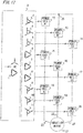
- FIG. 17 an example of circuit configuration of a first conventional power conversion device is shown.
- the power conversion device of FIG. 17 has a plural number of single-phase converters whose respective AC terminals are serially connected to each other.
- a plurality of mutually-insulated DC power sources are formed by a transformer having a plurality of windings and a plurality of diode rectifiers, and are connected to DC sections of the single-phase converters.
- the transformer is given as a transformer (phase-shifting transformer) including a plurality of windings 3 to 11 whose phases are shifted to each other (see, for example, Patent Document 1).
- FIG. 18 an example of circuit configuration of a second conventional power conversion device is shown.
- the power conversion device of FIG. 18 has a circuit configuration that is multiplexed using a plural number of three-phase converters having a common DC voltage and a plural number of three-phase transformers, in which secondary windings of the transformers are serially connected as open windings to each other (see, for example, Patent Document 2).
- FIG. 19 an example of circuit configuration of a third conventional power conversion device is shown.
- each of the single-phase transformers is connected at its primary side to other of the single-phase transformers in multi-serial fashion, and the serial ends are connected to input terminals, while a converter cell having a single-phase full-bridge converter/inverter that is configured, as shown in FIG. 20 , with legs capable of outputting a two-level voltage, is connected to the secondary winding of each of the single-phase transformer.
- the AC output terminal of each inverter is connected to the AC output terminal of each other inverter in multi-serial fashion (see, for example, Patent Document 3).
- the transformer (phase-shifting transformer) including a plurality of windings whose phases are mutually shifted, is required.
- the transformers are used in the output side, it is supposed that, when a motor or like load that requires voltage change is connected in the output side, its operation may be limited due to fear of magnetic saturation of the transformer. Specifically, such a case is considered where the power conversion device cannot output a low-frequency voltage.
- the third power conversion device of FIG. 19 since the self-commutated converters are used, a bidirectional power flow is enabled, whereas, since single-phase transformers are used, the number of the transformers increases.
- Patent Document 3 there is a statement that a three-phase transformer with a five-leg core is used in place of the single-phase transformer.
- the legs capable of outputting a two-level voltage is used in the converter cell, there is a drawback that an output voltage per one cell is low, so that the number of the converter cells and the number of the transformers increase.
- This invention has been made to solve the problems as described above, and an object thereof is to provide a power conversion device with high reliability, small size, light weight and low cost, and capable of performing regeneration operation as well, while not requiring such a structurally-complicated phase-shifting transformer, and suppressing increase in the number of the transformers.
- a power conversion device is a power conversion device which is adapted to perform power conversion between input terminals of multi-phase AC and output terminals of multi-phase AC, comprising: a voltage-transformer device including primary windings connected to the input terminals and secondary windings comprising pluralities of single-phase open windings that are insulated to each other; a plurality of converter cells including switching elements, in which their input ends are connected to the respective single-phase open windings, and their output ends are connected in mutually serial fashion to the output terminal of each phase, the converter cells each performing conversion between a single-phase AC and another single-phase AC; and a control circuit for controlling ON/OFF of the switching elements.
- the converter cells each comprise: a capacitor series connection; a converter that is adapted to convert a single- phase AC voltage from the input terminals into a three or more-level DC voltage and to output it to the capacitor series connection; and an inverter that is adapted to convert a DC voltage from the capacitor series connection into a single-phase AC voltage and outputs it to the output ends.
- the power conversion device according to the invention is configured as described above, so that the voltage-transformer device can be configured with a simple and light-weight structure. Further, since the converter cell is enabled to improve a voltage waveform and to accept a high-voltage specification, it is possible to suppress the generation of a harmonic component and to reduce the required number of the cells, to thereby achieve a power conversion device with small size, light weight and low cost.
- FIG. 1 an example of main circuit configuration of a power conversion device according to Embodiment 1 of the invention is shown.
- FIG. 1 shows a case where a three-phase voltage source 101 is connected to input terminals R, S, T of the power conversion device, and a three-phase motor 401 is connected to output terminals U, V, W. That is, FIG. 1 show a case where the power conversion device according to the invention is used as a motor drive device.
- each multi-phase alternating current (AC) applied to the input terminals and the output terminals is not limited to a three-phase AC.
- the invention of this application is also applicable to a circuit which includes, for example, three number of two-phase/two-phase transformers and six number of converter cells, so as to convert the two-phase AC coming through its input terminals into a three-phase AC and outputs it through its output terminals. Further, a serially-connected number of the converter cells is not limited to three.
- both the voltage source 101 and the motor 401 are of three-phase AC type, and three number of transformers 201, 202, 203 and three number of converter cells per one phase, i.e. total nine number of converter cells 30U1, 30U2, 30U3, 30V1, 30V2, 30V3, 30W1, 30W2, 30W3 are used.
- a control circuit 601 that controls ON/OFF of switching elements in the power conversion device is included therein.
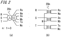
- FIG. 2(a) is a diagram showing an example of winding configuration of the transformer 20n, a detailed configuration of which is shown in FIG. 2(b) .
- Primary windings of the transformer 20n have a winding configuration of three-phase star connection (Y-connection) whose respective terminals are connected to the input terminals R, S, T of the power conversion device.
- Y-connection three-phase star connection
- Secondary windings comprise a plurality of single-phase open windings that are insulated to each other.
- voltages depending on the turn ratio are generated between Rs-Na, between Ss-Nb, and between Ts-Nc, according to voltages between the terminals R, S, T in the primary side and a neutral point N of the star connection, that is, the voltages between R-N, between S-N, and between T-N.
- one insulated-voltage source is formed per one secondary winding.
- it is not required to have three or more secondary windings, as the first conventional power conversion device shown in FIG. 17 does.
- a total leakage inductance of the primary winding and the secondary winding be designed to have a percent impedance of 5 % or more.
- Controllability of the current is mostly related to a percent impedance (inductance component in the output side of the converter cell 30Xn) and a switching frequency; the higher the either one of them becomes, the more the controllability is enhanced. That is, the percent impedance becomes an important factor to determine the controllability of the current.
- the switching frequency is generally restricted to some extent, and thus, as the percent impedance, about 5 % to 10 % is appropriate.
- a three or more-leg core is used as the core of the transformer 20n.
- a total voltage of the windings is not zero, there is a risk of causing magnetic saturation.
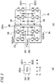
- FIG. 3(b) A detailed configuration of the main circuit of the converter cell 30Xn shown in FIG. 3(a) , is shown in FIG. 3(b) .
- the converter cell 30Xn has a converter 3a and an inverter 3b each being of a single-phase full-bridge type and having legs capable of outputting voltages of three levels or more, and performs conversion between a single-phase AC and another single-phase AC.
- the DC terminals of the converter 3a and the DC terminals of the inverter 3b are connected to a capacitor series connection CP-CN, respectively.
- the example of the converter cell 30Xn shown in FIG. 3 is based on the circuit of a diode-clamp type three-level converter in which switching elements SW with their respective free-wheel diodes FD inversely-parallel connected thereto, are connected in four series, and connected to a neutral point by each clamp diode CD.
- the diode-clamp type three-level converter utilizes four legs. Among these four legs, two legs are operated as the converter 3a.
- AC terminals IN1 and IN2 of the converter 3a which are input ends of the converter cell 30Xn, are connected to one secondary-side winding of the transformer 20n, for example, the single-phase open winding in FIG. 2 , at its both ends Rs and Na.
- the respective input ends of the converter cells 30Xn are connected in mutually parallel fashion to the input terminal of each phase, through the transformers 20n.
- the input ends of converter cells 30U1, 30U2, 30U3 are connected in mutually parallel fashion to the input terminal of R-phase through the transformers 201, 202, 203.
- Output terminals OUT1 and OUT2 of the inverter 3b which are output ends of the converter cell 30Xn, are serially connected to the output terminals of the other converter cells 30Xn of the same phase, and the three phases are star-connected while each phase is connected to each of the output terminals U, V, W of the power conversion device.
- the output ends of the converter cell 30Xn are connected in mutually serial fashion to the output terminal of each phase.
- the output ends of the converter cells 30U1, 30U2, 30U3 are connected in mutually serial fashion and are connected serially to the output terminal of U-phase.
- phase of the output terminal to which the output ends (inverter 3b-side) of the mutually serially-connected converter cell 30Xn are connected is the same as the phase of the input terminal to which the input ends (converter 3a-side) of the the converter cell 30Xn is connected.
- the input-side R phase is the same as the output-side U phase
- the input-side S phase is the same as the output-side V phase
- the input-side T phase is the same as the output-side W phase.
- the capacitor series connection CP-CN which is a series connection of a positive-side capacitor CP and a negative-side capacitor CN, is connected.
- the voltage applied between both ends of the capacitor series connection CP-CN is defined as a DC bus voltage
- the voltage applied to the positive-side capacitor CP is defined as a positive-side DC bus voltage
- the voltage applied to the negative-side capacitor CN is defined as a negative-side DC bus voltage.
- the power conversion device of the invention is made with the circuit configuration as described above, there are provided the following advantages. Because of using the converter cell 30Xn being a self-commutated inverter, it is possible to suppress a harmonic current in the input side by controlling ON/OFF of the switching devices SW in the converter 3a-side.
- phase-shifting transformer which is complicated in structure, large in size and high in cost, is unnecessary. Further, because of using the single-phase open windings as the secondary windings of the transformer 20n, it is possible to establish many voltage sources insulated to each other by a smaller number of windings.
- a single module in which a group of semiconductor elements are stored which includes a leg capable of outputting voltages of three levels, that is, the leg comprising four numbers of switching elements SW and free-wheel diodes FD, and two clamp diodes CD.
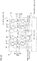
- the control circuit 601 has three main purposes, which are: to make closer the current flowing through the input terminal to an ideal sine wave (to reduce harmonic waves); to control the motor 401 to have an intended rotation speed or torque; and to control the DC bus voltages of the conversion cells 30Xn to have proper values to thereby prevent the semiconductor elements from causing overvoltage breakdown.
- control circuit 601 Using detection values of the current flowing through the input terminal or the conversion cell 30Xn of the power conversion device, the voltage at the input terminal of the power conversion device, and/or the DC bus voltages of the conversion cells (three voltages of the positive-side DC bus voltage, the negative-side DC bus voltage and a total voltage of both of them), the control circuit 601 finally develops gate signals for controlling ON/OFF of the switching elements SW of the converter cell 30Xn.
- the control circuit 601 includes: four control units of the input-current control unit 610, an output-voltage control unit 620, a bus-voltage control unit 630, and a modulation unit 640; further, the bus-voltage control unit 630 has an average-voltage control unit 631, an inter-phase balance control unit 632, an intra-phase balance control unit 633, and an intra-cell balance control unit 634.
- the processing by the input-current control unit 610 is reflected in controlling in the converter 3a-side, and the processing by the output-voltage control unit 620 is reflected in controlling in the inverter 3b-side.
- the processing by the average-voltage control unit 631 is reflected in controlling in the converter 3a-side
- the processing by inter-phase balance control unit 632 is reflected in controlling in the inverter 3b-side
- the processing by the intra-phase balance control unit 633 is reflected in controlling in the inverter 3b-side.
- the processing by the intra-cell balance control unit 634 is reflected in controlling in both or either one of the converter 3a-side and the inverter 3b-side.
- the processing by the modulation unit 640 is finally reflected in controlling the switching elements SW in the converter 3a-side and the inverter 3b-side.
- the voltages at the input terminals R, S, T are defined as Vr, Vs, Vt, and the currents flowing through the input terminals R, S, T are defined as Ir, Is, It.
- the DC bus voltages in the conversion cells 30Xn are defined as VdcXn, where "X” is one of U, V, and W, and "n" is one of 1, 2 and 3.
- voltage command values in the converter 3a-side of the converter cells 30Xn are defined as VCXn*, among which the voltage command values for the switching elements SW of the leg that outputs a voltage to the positive-side AC terminal IN1 (hereinafter, referred to as positive-side leg) are defined as VCXnP*, and the voltage command values for the switching elements SW of the leg that outputs a voltage to the AC terminal IN2 (hereinafter, referred to as negative-side leg) are defined as VCXnN* (see, FIG. 3(b) ).
- voltage command values in the inverter 3b-side are defined as VIXn*, among which the voltage command values for the switching elements SW of a positive-side leg are defined as VIXnP*, and the voltage command values for the switching elements SW of a negative-side leg are defined as VIXnN*.
- FIG. 5 A control block diagram showing an example of the input-current control unit 610 is shown in FIG. 5 .
- the main purpose of the input-current control unit 610 is to cause the currents IRsn, ISsn, ITsn flowing through the input terminals R, S, T or in the secondary side of the transformers 20n, to follow their current command values.
- the input-current control unit 610 controls them independently of the other set.
- a dq converter 51 makes a dq-conversion using a power-source phase ⁇ on these detection values, to thereby develop a d-axis current Idn and a q-axis current Iqn.
- the d-axis current corresponds to a reactive current (reactive power) and the q-axis current corresponds an active current (active power).
- Deviations between the acquired dq-axis currents Idn, Idq and their respective current command values Idn*, Iqn*, are calculated and provided to respective controllers Gc(s).
- the power-source voltages Vr, Vs, Vt are dq-converted by a dq converter 52, and are thereafter multiplied by a turn ratio TR of the transformer 20n, so that a d-axis voltage Vds and a q-axis voltage Vqs of the power-source voltages are acquired.
- the d-axis voltage Vds and the q-axis voltage Vqs of the power-source voltages are taken into consideration as a feedforward amount.
- the resultants are inversely dq-converted by a dq inverse converter 53, so that voltage commands values VCUn*, VCVn*, VCWn* in the converter 3a-side of the converter cells 30Xn are acquired.
- the transformer 20n since the transformer 20n is connected to the converter 3a-side, for the purpose of preventing its magnetic saturation, it is required not to output a zero-phase voltage thereto. Instead, the magnetic saturation may be prevented by controlling the zero-phase voltage that is developed from a total sum of the input currents IRsn, ISsn, ITsn, to be zero.
- FIG. 6 a control block diagram showing an example of the output-voltage control unit 620 is shown in FIG. 6 .
- total-voltage command values VIU*, VIV*, VIW* for the respective phases in the inverter 3b-side are acquired by a command value generation unit 61 using a publicly known motor control technique (for example, a constant V/f control, a vector control, a direct torque control, etc.). Further, a zero-phase voltage component Vz* having a three-fold output frequency is added to these voltage command values, so that the voltage-utilization ratio is enhanced.
- a publicly known motor control technique for example, a constant V/f control, a vector control, a direct torque control, etc.
- the bus-voltage control unit 630 controls the DC bus voltages in each converter cell 30Xn to become predetermined voltages, by means of four control units 631 to 634, i.e. the average-voltage control unit 631, the inter-phase balance control unit 632, the intra-phase balance control unit 633, and the intra-cell balance control unit 634.
- a control block diagram showing an example of the average-voltage control unit 631 is shown in FIG. 7 .
- an average value of the DC bus voltages VdcUn, VdcVn, VdcWn in the three converter cells 30Xn connected to one transformer 20n is calculated by an average-value calculator 71.
- a q-axis current command value Iqn* that corresponds to an input-current active component in the primary windings of the transformer 20n, is determined so that the average value VdcAVGn is caused to follow a predetermined bus voltage command value Vdc*. Specifically, a deviation between VdcAVGn and Vdc* is calculated, which is then provided to a controller Gv(s) where Iqn* is calculated.
- controller Gv(s) a PI controller or the like, may be used. Since Iqn* is a current corresponding to the active power, it is possible to cause VdcAVGn to follow Vdc*. Note that, when a PQ conversion is applied to the input-current control unit 610 as described above, a command value P* of the active power is adjusted.
- the mutual converter cells 30Xn serially connected in the inverter 3b-side are connected in the converter 3a-side in parallel through the transformer 20n, and every common converter cells connected in mutually serial and parallel fashion are connected to a same phase.
- the average-voltage control unit 631 performs controlling while regarding the three number of the converter cells 30Xn connected to one transformer 20n as one set. As a result, when the average value of the DC bus voltages VdcAVGn is determined, voltage oscillations that emerge in the respective DC bus voltages become negated.
- the inter-phase balance control unit 632 adjusts the zero-phase voltage Vzb* that overlaps the voltage command value for each phase in the inverter 3b-side (see, FIG. 6 ), to thereby balance the average voltages of the DC bus voltages in the respective phases: VdcUAVG (average value of VdcU1 to VdcU3), VdcVAVG (average value of VdcV1 to VdcV3) and VdcWAVG (average value of VdcW1 to VdcW3), evenly to each other.
- VdcUAVG average value of VdcU1 to VdcU3
- VdcVAVG average value of VdcV1 to VdcV3
- VdcWAVG average value of VdcW1 to VdcW3
- the average voltages of VdcUAVG, VdcVAVG, VdcWAVG in the respective phases are calculated by respective calculators 81, and the total average voltage VdcAVG is further calculated by a calculator 82.
- the zero-phase voltage command vale Vzb* is acquired by calculating the products of the outputs of the controllers Gp(s) and the voltage command values VIU*, VIV*, VIW* in the inverter 3b-side, respectively for each phase, followed by summing up the resultants.
- the reason of providing processing by the LPF is, as described above, for removing the frequency component that has emerged in the DC bus voltage and is twice the output frequency.
- the controller Gp(s) a PI controller or the like, may be used.
- FIG. 9 a control block diagram showing an example of the intra-phase balance control unit 633 is shown in FIG. 9 .
- the intra-phase balance control unit 633 adjusts the shared output voltages of the inverters 3b in each phase, to thereby balance the DC bus voltages in the phase evenly to each other.
- the deviations between the respective DC bus voltages VdcX1 to VdcX3 in the phase and the bus-voltage average value VdcXAVG in the phase are respectively calculated, which are then provided to controllers Gb(s).
- the resultants are equivalent to an adjusted ratio of the shared output voltages, so that adjustment ranges are developed by multiplying them respectively by the voltage command value VIX** provisionally determined by the output-voltage control unit 620 (see, FIG. 6 ).
- the adjustment ranges are developed by multiplying them respectively by the voltage command value VIX** provisionally determined by the output-voltage control unit 620 (see, FIG. 6 ).
- the final voltage command values VIX1*, VIX2*, VIX3* are developed.
- an output voltage of the inverter 3b in the converter cell 30Xn whose DC bus voltage is relatively small becomes smaller, so that the output power can be suppressed.
- the DC bus voltages in the phase can be balanced to each other.
- the intra-cell balance control unit 634 serves to balance the positive-side DC bus voltage and the negative-side DC bus voltage evenly to each other, by adjusting the ratio of the voltages in the positive-side leg and the negative-side leg. This controlling can be realized by it being reflected on either one or both of the converter 3a-side and the inverter 3b-side.
- a deviation between a negative-side DC bus voltage VdcXnN, which is a voltage to be applied to the negative-side capacitor CN, and a positive-side DC bus voltage VdcXnP, which is a voltage to be applied to the positive-side capacitor CP, is calculated, which is then provided to a controller Gcz(s), so that VXnCz* is calculated.
- VXnCz* is added to the respective voltage command values VXnP*, VXnN*, respectively, so that the final voltage command value VCXnP* of the positive leg and the final voltage command value VCXnN* of the negative leg are calculated.
- the voltage command value of the low-voltage capacitor side is increased, thereby making it possible to balance the DC bus voltages in the positive side and in the negative side.
- FIG. 11 shows an example of controlling by the modulation unit 640; in particular, FIG. 11(a) shows the controlling for converter 3a-side and FIG. 11(b) shows the controlling for inverter 3b-side.
- the modulation unit 640 performs a pulse width modulation (PWM) on the basis of the voltage command values VCXnP*, VCXnN* in the converter 3a-side and the voltage command values VIXnP*, VIXnN* in the inverter 3b-side, which have been developed by the aforementioned respective control units 610 to 630, to thereby develop gate signals for controlling ON/OFF of the respective switching elements SW.
- PWM pulse width modulation
- the modulation unit 640 provides the respective voltage command values to a PWM converter 801 (in the converter 3a-side) or a PWM converter 802 (in the inverter 3b-side), and further applies a dead time processing respectively to the resultants so that they have delays in their leading edges, to thereby output the gate signals for controlling ON/OFF of the respective switching elements SW.
- What is intended by the modulation unit 640 is as follows: to cause the switching timings not to overlap between the positive-side leg and the negative-side leg, as much as possible; to cause the switching timings not to overlap between the converters 3a connected in parallel through the transformers 20n, as much as possible; and to cause the respective switching timings not to overlap between the serially connected inverters 3b; to thereby achieve the input current and/or output voltage with little harmonic component.
- FIG. 12 shows controlling in the converter 3a-side
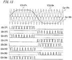
- FIG. 13 shows controlling in the inverter 3b-side.
- the triangle-wave carriers CarCPn, CarCNn are compared with the voltage command value VCXnP* of the positive-side leg and the voltage command value VCXnN* of the negative-side leg, respectively.
- the two triangle- wave carriers CarCPn, CarCNn have the same phase, the amplitude of the triangle-wave carrier CarCPn for the positive-voltage output corresponds to a voltage across the positive-side capacitor CP in the converter cell 30Xn concerned, and the amplitude of the triangle-wave carrier CarCNn for the negative-voltage output corresponds to a voltage across the negative-side capacitor CN.
- the gate signals to the respective four switching elements SW of the positive-side leg in the converter 3a-side are defined as GXnCP1, GXnCP2, GXnCP3 and GXnCP4, in the order from the switching element SW in the side of the positive DC terminal.
- gate signals to the respective four switching elements SW of the negative-side leg are defined as GXnCN1, GXnCN2, GXnCN3 and GXnCN4, in the order from the switching element SW in the side of the positive DC terminal.
- the gate signals GXnCP1, GXnCP3 are determined from a magnitude relationship between the triangle-wave carrier CarCPn for the positive-voltage output and the voltage command value VCXnP* of the positive-side leg.
- the gate signals GXnCP2, GXnCP4 are determined from a magnitude relationship between the triangle-wave carrier CarCNn for the negative-voltage output and the voltage command value VCXnP* of the positive-side leg.
- the gate signals GXnCN1, GXnCN3 are determined from a magnitude relationship between the triangle-wave carrier CarCPn for the positive-voltage output and the voltage command value VCXnN* of the negative-side leg.
- the gate signals GXnCN2, GXnCN4 are determined from a magnitude relationship between the triangle-wave carrier CarCNn for the negative-voltage output and the voltage command value VCXnN* of the negative-side leg.
- the dead time processing is applied to the respective gate signals so as to have delays in their leading edges, so that the final gate signals are determined. Because of being publicly known, the dead time processing is omitted from the description.
- the triangle-wave carriers CarIPn, CarINn are compared to the voltage command value VIXnP* of the positive-side leg and the voltage command value VIXnN* of the negative-side leg, respectively.
- the two triangle-wave carriers CarIPn, CarINn have the same phase, the amplitude of the triangle-wave carrier CarIPn for the positive-voltage output corresponds to the voltage across the positive- side capacitor CP in the converter cell 30Xn concerned, and the amplitude of the triangle-wave carrier CarINn for the negative-voltage output corresponds to the voltage across the negative-side capacitor CN.
- the gate signals to the respective four switching elements SW of the positive-side leg in the inverter 3b-side are defined as GXnIP1, GXnIP2, GXnIP3 and GXnIP4, in the order from the switching element SW in the side of the positive DC terminal.
- gate signals to the respective four switching elements SW of the negative-side leg are defined as GXnINI, GXnIN2, GXnIN3 and GXnIN4, in the order from the switching element SW in the side of the positive DC terminal.
- the gate signals GXnIP1, GXnCI3 are determined from a magnitude relationship between the triangle-wave carrier CarIPn for the positive-voltage output and the voltage command value VIXnP* of the positive-side leg.
- the gate signals GXnIP2, GXnIP4 are determined from a magnitude relationship between the triangle-wave carrier CarINn for the negative-voltage output and the voltage command value VIXnP* of the positive-side leg.
- the gate signals GXnINI, GXnIN3 are determined from a magnitude relationship between the triangle-wave carrier CarIPn for the positive-voltage output and the voltage command value VIXnN* of the negative-side leg.
- the gate signals GXnIN2, GXnIN4 are determined from a magnitude relationship between the triangle-wave carrier CarINn for the negative-voltage output and the voltage command value VIXnN* of the negative-side leg.
- the positive-side switching element SW When the voltage command value is larger than the triangle-wave carrier, the positive-side switching element SW is turned ON and the negative-side switching element SW is turned OFF, whereas in the reverse case of magnitude relationship, ON/OFF operation is reversed. Finally, the dead time processing is applied, to thereby determine the final gate signals.
- a phase relationship between the triangle-wave carriers is important.
- a harmonic component near the carrier frequency is dominant.
- the respective voltage command values of the positive-side leg and negative-side leg are in a nearly reverse relationship (negative-side value is calculated by multiplying "-1"), and thus the carrier frequency components are equivalently negated therebetween, so that a harmonic component having a near two-fold frequency of the carrier frequency becomes dominant.
- FIG. 14(a) shows controlling in the converter 3a-side
- FIG. 14(b) shows controlling in the inverter 3b-side.
- the remaining harmonic component has a near six-fold frequency of the carrier frequency, which is a much higher frequency, it is easily removable by adding small filters in the input terminals or the converter 3a-side of the converter cell 30Xn.
- serial connections are provided in the inverter 3b-side, by shifting switching timings, it is possible to increase the output voltage levels according to the number of potentials that the capacitors have.
- the power conversion device As described above, by using the power conversion device according to the invention, a conventional phase-shifting transformer which is complicated in structure becomes unnecessary. Further, by configuring the converter cell 30Xn to be a three or more-level converter, it is possible to reduce the number of the converter cells 30Xn and the number of windings in the transformer 20n, to thereby achieve downsizing, weight-saving and cost reduction.
- FIG. 15 An example of a main circuit configuration of a power conversion device according to Embodiment 2 of the invention is shown in FIG. 15 .
- the voltage-transformer device is different from the voltage-transformer device (transformers 20n) shown in FIG. 1 of Embodiment 1.
- FIG. 16(a) is a diagram showing an example of wiring configuration of a transformer 211 as the voltage- transformer device according to Embodiment 2, a detailed configuration of which is shown in FIG. 16(b) .
- primary windings of the transformer 211 have a winding configuration of a three-phase star connection (Y-connection).
- secondary windings comprising a plurality of windings (three, here) per one phase of the primary winding, to thereby have a configuration corresponding to that collecting the transformers 201, 202, 203 into the one transformer 211.
- the secondary windings comprises three single-phase open windings per one phase, so that by the one transformer 211, power sources comprising in total nine single-phase open windings insulated to each other, are established.
- Embodiment 1 with respect to each set of converter cells 30Xn connected to one transformer 20n (for example, the set of 30U1, 30V1, 30W1), the input-current control unit 610 is used.
- a three or more-leg core is usable as the core of the transformer, and it is desirable that the leakage inductance be given as about 5 % or more.
- an additional reactor may be introduced. This may be introduced in the primary side of the transformer, or introduced in the secondary side thereof.
- an LC filter may be introduced in the primary side or the secondary side.
- an IGBT Insulated Gate Bipolar Transistor
- MOSFET Metal Oxide Semiconductor Field Effect Transistor
- silicon is generally used as a material of the semiconductor element constituting the switching element SW and the diodes FD,CD
- a wide bandgap material such as a silicon carbide, a gallium nitride family material or diamond, whose bandgap is wider than that of silicon, is used, it is possible to increase the breakdown voltage of the semiconductor element, so that the number of the aforementioned converter cells 30Xn can be further reduced.
- the effects are achieved by applying the material to either one or both of the converter 3a and the inverter 3b of the converter cell 30Xn.
Priority Applications (1)
| Application Number | Priority Date | Filing Date | Title |
|---|---|---|---|
| EP18176497.8A EP3389174A1 (de) | 2013-06-04 | 2013-06-04 | Stromwandlungsvorrichtung |
Applications Claiming Priority (3)
| Application Number | Priority Date | Filing Date | Title |
|---|---|---|---|
| EP18176497.8A EP3389174A1 (de) | 2013-06-04 | 2013-06-04 | Stromwandlungsvorrichtung |
| EP13872277.2A EP2835902A4 (de) | 2013-06-04 | 2013-06-04 | Stromwandler |
| PCT/JP2013/065429 WO2014196013A1 (ja) | 2013-06-04 | 2013-06-04 | 電力変換装置 |
Related Parent Applications (1)
| Application Number | Title | Priority Date | Filing Date |
|---|---|---|---|
| EP13872277.2A Division EP2835902A4 (de) | 2013-06-04 | 2013-06-04 | Stromwandler |
Publications (1)
| Publication Number | Publication Date |
|---|---|
| EP3389174A1 true EP3389174A1 (de) | 2018-10-17 |
Family
ID=52007689
Family Applications (2)
| Application Number | Title | Priority Date | Filing Date |
|---|---|---|---|
| EP18176497.8A Ceased EP3389174A1 (de) | 2013-06-04 | 2013-06-04 | Stromwandlungsvorrichtung |
| EP13872277.2A Ceased EP2835902A4 (de) | 2013-06-04 | 2013-06-04 | Stromwandler |
Family Applications After (1)
| Application Number | Title | Priority Date | Filing Date |
|---|---|---|---|
| EP13872277.2A Ceased EP2835902A4 (de) | 2013-06-04 | 2013-06-04 | Stromwandler |
Country Status (6)
| Country | Link |
|---|---|
| US (1) | US9712070B2 (de) |
| EP (2) | EP3389174A1 (de) |
| CN (1) | CN104380586B (de) |
| RU (1) | RU2594359C2 (de) |
| WO (1) | WO2014196013A1 (de) |
| ZA (1) | ZA201403943B (de) |
Cited By (1)
| Publication number | Priority date | Publication date | Assignee | Title |
|---|---|---|---|---|
| CN113452262A (zh) * | 2021-07-05 | 2021-09-28 | 珠海格力电器股份有限公司 | 一种变频器及其升压控制方法、电机 |
Families Citing this family (37)
| Publication number | Priority date | Publication date | Assignee | Title |
|---|---|---|---|---|
| EP3005543B1 (de) * | 2013-07-15 | 2020-03-25 | Siemens Aktiengesellschaft | Modularer multilevel dc/dc wandler für hvdc anwendungen |
| US10075117B2 (en) * | 2014-02-03 | 2018-09-11 | Johnson Controls Technology Company | Multi-pulse constant voltage transformer for a variable speed drive in chiller applications |
| CN105990846B (zh) * | 2014-09-05 | 2018-10-09 | 台达电子工业股份有限公司 | 风电变流器装置和变流器装置 |
| US9768706B2 (en) * | 2014-09-05 | 2017-09-19 | Delta Electronics, Inc. | Wind power converter device and converter device |
| JP6331925B2 (ja) * | 2014-09-25 | 2018-05-30 | 株式会社安川電機 | マトリクスコンバータ、発電システムおよび電力変換方法 |
| JP6515549B2 (ja) * | 2015-01-22 | 2019-05-22 | 富士電機株式会社 | マルチ出力電源装置 |
| US9831812B2 (en) * | 2015-02-27 | 2017-11-28 | Nutech Ventures | Direct torque control of AC electric machines |
| CN104702123B (zh) * | 2015-03-23 | 2018-06-08 | 深圳市英威腾电气股份有限公司 | 一种三电平功率单元主回路、功率单元以及高压变频器 |
| EP3291437B1 (de) * | 2015-04-27 | 2023-01-11 | Mitsubishi Electric Corporation | Drehmaschinensteuerungsvorrichtung und elektrische servolenkungsvorrichtung |
| JP6522141B2 (ja) * | 2015-09-17 | 2019-05-29 | 三菱電機株式会社 | 電力変換装置 |
| JP6522140B2 (ja) * | 2015-09-17 | 2019-05-29 | 三菱電機株式会社 | 電力変換装置 |
| EP3352359B1 (de) * | 2015-09-17 | 2020-09-16 | Mitsubishi Electric Corporation | Stromwandlungsvorrichtung |
| CN105222889B (zh) * | 2015-10-12 | 2018-05-15 | 绍兴文理学院 | 一种强激光功率密度的测量装置 |
| WO2017168518A1 (ja) * | 2016-03-28 | 2017-10-05 | 三菱電機株式会社 | 電力変換装置 |
| JP6852445B2 (ja) * | 2017-02-16 | 2021-03-31 | 富士電機株式会社 | 半導体装置 |
| CN107340420B (zh) * | 2017-07-19 | 2023-11-28 | 广东美的暖通设备有限公司 | 三相电压检测电路和空调器 |
| WO2019026764A1 (ja) * | 2017-08-04 | 2019-02-07 | パナソニックIpマネジメント株式会社 | 電力変換装置、及び電力変換システム |
| JP7004561B2 (ja) * | 2017-12-12 | 2022-01-21 | 株式会社日立インダストリアルプロダクツ | 電力変換装置 |
| US11218079B2 (en) * | 2018-03-09 | 2022-01-04 | Toshiba Mitsubishi-Electric Industrial Systems Corporation | Power conversion device |
| JP6906464B2 (ja) * | 2018-03-15 | 2021-07-21 | 株式会社東芝 | 電力変換装置の制御装置および制御方法 |
| JP7070004B2 (ja) * | 2018-04-13 | 2022-05-18 | 株式会社安川電機 | 電力変換装置及び電力変換方法 |
| FI128052B (en) * | 2018-04-16 | 2019-08-30 | Lappeenrannan Teknillinen Yliopisto | Power converter for a bioelectrochemical system |
| CN112154598B (zh) * | 2018-05-21 | 2024-04-16 | 三菱电机株式会社 | 功率转换装置 |
| RU2699012C1 (ru) * | 2018-11-26 | 2019-09-03 | Илья Николаевич Джус | Трехфазный частотный преобразователь высокого напряжения |
| FR3090244B1 (fr) * | 2018-12-14 | 2020-11-13 | Schneider Toshiba Inverter Europe Sas | Gestion de nombre de cellules de puissance actives d’un variateur de vitesse |
| CN109742968B (zh) * | 2019-01-31 | 2020-12-04 | 上海交通大学 | 二极管箝位混合三电平双有源全桥变流器及其控制方法 |
| CN111837327B (zh) * | 2019-02-15 | 2023-12-08 | 东芝三菱电机产业系统株式会社 | 电力转换装置、电动机驱动系统及控制方法 |
| US10651760B1 (en) * | 2019-04-24 | 2020-05-12 | Rockwell Automation Technologies, Inc | Reduced semiconductor device power cell voltage drive |
| US10924025B2 (en) * | 2019-04-24 | 2021-02-16 | Rockwell Automation Technologies, Inc. | Regenerative cascaded H bridge power supply |
| EP4029139A4 (de) | 2019-09-13 | 2023-09-27 | Milwaukee Electric Tool Corporation | Stromwandler mit halbleitern mit breiter bandlücke |
| RU2717338C1 (ru) * | 2019-11-16 | 2020-03-23 | Федеральное государственное бюджетное образовательное учреждение высшего образования «Государственный университет морского и речного флота имени адмирала С.О. Макарова» | Каскадный преобразователь частоты |
| CN112928898A (zh) * | 2019-12-06 | 2021-06-08 | 中兴通讯股份有限公司 | 功率变换器的bus电压均衡调节方法及功率变换器 |
| RU2717085C1 (ru) * | 2019-12-17 | 2020-03-18 | Илья Николаевич Джус | Многоблочный трехфазный частотный преобразователь |
| RU2723304C1 (ru) * | 2020-01-17 | 2020-06-09 | Илья Николаевич Джус | Способ поочередного управления трехфазным частотным преобразователем |
| RU2718518C1 (ru) * | 2020-01-17 | 2020-04-08 | Илья Николаевич Джус | Трехфазный многоблочный частотный преобразователь |
| RU2724604C1 (ru) * | 2020-02-26 | 2020-06-25 | Илья Николаевич Джус | Трехфазный частотный преобразователь высокого напряжения |
| RU2744721C1 (ru) * | 2020-10-08 | 2021-03-15 | Илья Николаевич Джус | Строенная трансформаторная группа (варианты) |
Citations (9)
| Publication number | Priority date | Publication date | Assignee | Title |
|---|---|---|---|---|
| US5625545A (en) | 1994-03-01 | 1997-04-29 | Halmar Robicon Group | Medium voltage PWM drive and method |
| DE19832226A1 (de) * | 1998-07-17 | 2000-01-20 | Semikron Elektronik Gmbh | Vierquadrantenumrichter für mittlere und höhere Spannungen |
| JP3019655B2 (ja) | 1992-07-23 | 2000-03-13 | 株式会社日立製作所 | 電力変換装置 |
| CN1400731A (zh) * | 2001-08-07 | 2003-03-05 | 任少康 | 一种波形发生方法及电力变换装置 |
| JP2009106081A (ja) | 2007-10-23 | 2009-05-14 | Mitsubishi Heavy Ind Ltd | 電力変換器 |
| CN102158097A (zh) * | 2011-04-07 | 2011-08-17 | 李永盼 | 一种能量回馈型功率单元串联高压变频器 |
| US20120033472A1 (en) * | 2010-08-05 | 2012-02-09 | Toshiba International Corporation | Multi-Phase Drive System |
| US20120106223A1 (en) * | 2010-10-29 | 2012-05-03 | Converteam Gmbh | Circuit for converting power between a three-phase grid and a single-phase grid |
| US20130121041A1 (en) * | 2011-11-15 | 2013-05-16 | General Electric Company | Power converter based on h-bridges |
Family Cites Families (23)
| Publication number | Priority date | Publication date | Assignee | Title |
|---|---|---|---|---|
| CH666147A5 (de) | 1983-09-08 | 1988-06-30 | Bbc Brown Boveri & Cie | Hochspannungs-gleichstromversorgung mit ueberstromschutz. |
| JPH04188206A (ja) * | 1990-11-22 | 1992-07-06 | Hitachi Ltd | 電源装置 |
| JPH04271281A (ja) | 1991-02-25 | 1992-09-28 | Sansha Electric Mfg Co Ltd | 電源装置 |
| JPH0543734U (ja) | 1991-11-08 | 1993-06-11 | 日新電機株式会社 | 直列式電圧変動対策装置 |
| JP3723983B2 (ja) | 1995-09-08 | 2005-12-07 | 株式会社安川電機 | 直列多重3相pwmサイクロコンバータ |
| JP3937236B2 (ja) * | 1995-09-08 | 2007-06-27 | 株式会社安川電機 | 直列多重3相pwmサイクロコンバータ装置および直列多重3相pwmサイクロコンバータ装置の運転方法および直列多重3相pwm電力変換装置 |
| JP3431506B2 (ja) | 1998-07-28 | 2003-07-28 | 株式会社東芝 | 多重インバータ装置 |
| JP3536695B2 (ja) | 1998-12-16 | 2004-06-14 | 三菱電機株式会社 | 可変速装置 |
| JP2000228883A (ja) * | 1999-02-04 | 2000-08-15 | Fuji Electric Co Ltd | 電力変換装置 |
| US6236580B1 (en) * | 1999-04-09 | 2001-05-22 | Robicon Corporation | Modular multi-level adjustable supply with series connected active inputs |
| US6313600B1 (en) * | 2000-02-29 | 2001-11-06 | Robicon Corporation | Control method and apparatus for insufficient input voltage in an AC drive |
| KR20080109878A (ko) * | 2006-04-25 | 2008-12-17 | 미쓰비시덴키 가부시키가이샤 | 전력 변환 장치 |
| US7830681B2 (en) * | 2008-09-24 | 2010-11-09 | Teco-Westinghouse Motor Company | Modular multi-pulse transformer rectifier for use in asymmetric multi-level power converter |
| JP5136384B2 (ja) | 2008-12-16 | 2013-02-06 | 株式会社明電舎 | 直列多重インバータの出力電流検出方法 |
| WO2010082265A1 (ja) * | 2009-01-13 | 2010-07-22 | 三菱電機株式会社 | 電力変換装置 |
| RU2402146C1 (ru) * | 2009-04-08 | 2010-10-20 | Государственное образовательное учреждение высшего профессионального образования "Норильский индустриальный институт" | Преобразователь постоянного напряжения в переменное синусоидальное |
| US8605461B2 (en) * | 2009-09-28 | 2013-12-10 | Daikin Industries, Ltd. | Phase current detection device and power conversion device using the same |
| WO2011111175A1 (ja) | 2010-03-09 | 2011-09-15 | 三菱電機株式会社 | パワー半導体モジュール、電力変換装置および鉄道車両 |
| RU110880U1 (ru) * | 2011-06-10 | 2011-11-27 | Государственное образовательное учреждение высшего профессионального образования "Саратовский государственный технический университет" (СГТУ) | Трехфазный сложномостовой инвертор напряжения |
| JP2013042610A (ja) * | 2011-08-18 | 2013-02-28 | Sanken Electric Co Ltd | 電力変換装置 |
| US9099938B2 (en) * | 2011-12-16 | 2015-08-04 | Empower Micro Systems | Bi-directional energy converter with multiple DC sources |
| US20130258729A1 (en) * | 2012-03-29 | 2013-10-03 | Delta Electronics, Inc. | Medium voltage power apparatus |
| US9083274B2 (en) * | 2013-04-08 | 2015-07-14 | Rockwell Automation Technologies, Inc. | Power stage precharging and dynamic braking apparatus for multilevel inverter |
-
2013
- 2013-06-04 CN CN201380009116.5A patent/CN104380586B/zh active Active
- 2013-06-04 RU RU2014133045/07A patent/RU2594359C2/ru active
- 2013-06-04 US US14/359,649 patent/US9712070B2/en active Active
- 2013-06-04 EP EP18176497.8A patent/EP3389174A1/de not_active Ceased
- 2013-06-04 WO PCT/JP2013/065429 patent/WO2014196013A1/ja active Application Filing
- 2013-06-04 EP EP13872277.2A patent/EP2835902A4/de not_active Ceased
-
2014
- 2014-05-29 ZA ZA2014/03943A patent/ZA201403943B/en unknown
Patent Citations (9)
| Publication number | Priority date | Publication date | Assignee | Title |
|---|---|---|---|---|
| JP3019655B2 (ja) | 1992-07-23 | 2000-03-13 | 株式会社日立製作所 | 電力変換装置 |
| US5625545A (en) | 1994-03-01 | 1997-04-29 | Halmar Robicon Group | Medium voltage PWM drive and method |
| DE19832226A1 (de) * | 1998-07-17 | 2000-01-20 | Semikron Elektronik Gmbh | Vierquadrantenumrichter für mittlere und höhere Spannungen |
| CN1400731A (zh) * | 2001-08-07 | 2003-03-05 | 任少康 | 一种波形发生方法及电力变换装置 |
| JP2009106081A (ja) | 2007-10-23 | 2009-05-14 | Mitsubishi Heavy Ind Ltd | 電力変換器 |
| US20120033472A1 (en) * | 2010-08-05 | 2012-02-09 | Toshiba International Corporation | Multi-Phase Drive System |
| US20120106223A1 (en) * | 2010-10-29 | 2012-05-03 | Converteam Gmbh | Circuit for converting power between a three-phase grid and a single-phase grid |
| CN102158097A (zh) * | 2011-04-07 | 2011-08-17 | 李永盼 | 一种能量回馈型功率单元串联高压变频器 |
| US20130121041A1 (en) * | 2011-11-15 | 2013-05-16 | General Electric Company | Power converter based on h-bridges |
Non-Patent Citations (1)
| Title |
|---|
| ALBERT MARTIN RUBAN A ET AL: "Real time Harmonic Elimination PWM control for Voltage Source Inverters", 2012 INTERNATIONAL CONFERENCE ON ADVANCES IN ENGINEERING, SCIENCE AND MANAGEMENT (ICAESM 2012) : NAGAPATTINAM, TAMIL NADU, INDIA, 30 - 31 MARCH 2012, IEEE, PISCATAWAY, NJ, 30 March 2012 (2012-03-30), pages 479 - 484, XP032185521, ISBN: 978-1-4673-0213-5 * |
Cited By (2)
| Publication number | Priority date | Publication date | Assignee | Title |
|---|---|---|---|---|
| CN113452262A (zh) * | 2021-07-05 | 2021-09-28 | 珠海格力电器股份有限公司 | 一种变频器及其升压控制方法、电机 |
| CN113452262B (zh) * | 2021-07-05 | 2022-07-15 | 珠海格力电器股份有限公司 | 一种变频器及其升压控制方法、电机 |
Also Published As
| Publication number | Publication date |
|---|---|
| US9712070B2 (en) | 2017-07-18 |
| EP2835902A4 (de) | 2016-05-11 |
| ZA201403943B (en) | 2016-07-27 |
| CN104380586A (zh) | 2015-02-25 |
| WO2014196013A1 (ja) | 2014-12-11 |
| RU2594359C2 (ru) | 2016-08-20 |
| BR112014016286A8 (pt) | 2017-07-04 |
| CN104380586B (zh) | 2017-12-12 |
| BR112014016286A2 (pt) | 2017-06-13 |
| US20150236603A1 (en) | 2015-08-20 |
| RU2014133045A (ru) | 2016-02-27 |
| EP2835902A1 (de) | 2015-02-11 |
Similar Documents
| Publication | Publication Date | Title |
|---|---|---|
| US9712070B2 (en) | Power conversion device | |
| JP6181132B2 (ja) | 電力変換装置 | |
| EP2816719B1 (de) | Verbesserte mehrstufige Spannungsquellenwandler und Systeme | |
| US6236580B1 (en) | Modular multi-level adjustable supply with series connected active inputs | |
| Floricau et al. | New multilevel converters with coupled inductors: Properties and control | |
| EP0852425B1 (de) | Stromwandlervorrichtung und -verfahren | |
| Basu et al. | A high-frequency link single-stage PWM inverter with common-mode voltage suppression and source-based commutation of leakage energy | |
| JP5762329B2 (ja) | 電力変換装置 | |
| JP5450157B2 (ja) | 電力変換装置 | |
| US20140268888A1 (en) | Converter bridge arm suitable for high-voltage applications and application system thereof | |
| EP2451071B1 (de) | Steuerungsverfahren zur Stromumwandlung und zur Durchführung des besagten Verfahrens angepasster Elektrostromwandler | |
| US10218285B2 (en) | Medium voltage hybrid multilevel converter and method for controlling a medium voltage hybrid multilevel converter | |
| US10177684B2 (en) | Converter for an AC system | |
| KR100970566B1 (ko) | 전력회생이 가능한 h-브리지 방식의 멀티레벨 컨버터 | |
| JP2008295149A (ja) | 多重電力変換装置、及び多重変圧器 | |
| JP6104736B2 (ja) | 電力変換装置 | |
| WO2014082661A1 (en) | Phase converter with transformer coupled cells, hv ac/dc converter and associated method | |
| Ding et al. | A new current source converter using AC-type flying-capacitor technique | |
| Muneshima et al. | A multilevel AC-AC conversion system and control method using Y-connected H-bridge circuits and bidirectional switches | |
| JP4178331B2 (ja) | 直列多重パルス幅変調サイクロコンバータ装置およびその制御方法 | |
| KR102261327B1 (ko) | 인버터 시스템 | |
| JP2003324990A (ja) | 可変速駆動装置 | |
| Chai et al. | Space vector PWM for three-to-five phase indirect matrix converters with d 2-q 2 vector elimination | |
| CN111865098A (zh) | 再生级联h桥电力供应装置 | |
| Wang et al. | Analysis of Modulation Schemes for Balanced Inverter |
Legal Events
| Date | Code | Title | Description |
|---|---|---|---|
| PUAI | Public reference made under article 153(3) epc to a published international application that has entered the european phase |
Free format text: ORIGINAL CODE: 0009012 |
|
| STAA | Information on the status of an ep patent application or granted ep patent |
Free format text: STATUS: THE APPLICATION HAS BEEN PUBLISHED |
|
| AC | Divisional application: reference to earlier application |
Ref document number: 2835902 Country of ref document: EP Kind code of ref document: P |
|
| AK | Designated contracting states |
Kind code of ref document: A1 Designated state(s): AL AT BE BG CH CY CZ DE DK EE ES FI FR GB GR HR HU IE IS IT LI LT LU LV MC MK MT NL NO PL PT RO RS SE SI SK SM TR |
|
| STAA | Information on the status of an ep patent application or granted ep patent |
Free format text: STATUS: REQUEST FOR EXAMINATION WAS MADE |
|
| 17P | Request for examination filed |
Effective date: 20190415 |
|
| RBV | Designated contracting states (corrected) |
Designated state(s): AL AT BE BG CH CY CZ DE DK EE ES FI FR GB GR HR HU IE IS IT LI LT LU LV MC MK MT NL NO PL PT RO RS SE SI SK SM TR |
|
| STAA | Information on the status of an ep patent application or granted ep patent |
Free format text: STATUS: EXAMINATION IS IN PROGRESS |
|
| 17Q | First examination report despatched |
Effective date: 20191115 |
|
| STAA | Information on the status of an ep patent application or granted ep patent |
Free format text: STATUS: EXAMINATION IS IN PROGRESS |
|
| STAA | Information on the status of an ep patent application or granted ep patent |
Free format text: STATUS: EXAMINATION IS IN PROGRESS |
|
| STAA | Information on the status of an ep patent application or granted ep patent |
Free format text: STATUS: THE APPLICATION HAS BEEN REFUSED |
|
| 18R | Application refused |
Effective date: 20221103 |