EP3357086B1 - Verfahren zur kapazitiver kopplung von chipkomponenten einer integrierten schaltung - Google Patents
Verfahren zur kapazitiver kopplung von chipkomponenten einer integrierten schaltung Download PDFInfo
- Publication number
- EP3357086B1 EP3357086B1 EP16852270.4A EP16852270A EP3357086B1 EP 3357086 B1 EP3357086 B1 EP 3357086B1 EP 16852270 A EP16852270 A EP 16852270A EP 3357086 B1 EP3357086 B1 EP 3357086B1
- Authority
- EP
- European Patent Office
- Prior art keywords
- dielectric
- layer
- integrated circuit
- circuit dies
- etch stop
- Prior art date
- Legal status (The legal status is an assumption and is not a legal conclusion. Google has not performed a legal analysis and makes no representation as to the accuracy of the status listed.)
- Active
Links
Images




Classifications
-
- H—ELECTRICITY
- H10—SEMICONDUCTOR DEVICES; ELECTRIC SOLID-STATE DEVICES NOT OTHERWISE PROVIDED FOR
- H10W—GENERIC PACKAGES, INTERCONNECTIONS, CONNECTORS OR OTHER CONSTRUCTIONAL DETAILS OF DEVICES COVERED BY CLASS H10
- H10W90/00—Package configurations
-
- H—ELECTRICITY
- H10—SEMICONDUCTOR DEVICES; ELECTRIC SOLID-STATE DEVICES NOT OTHERWISE PROVIDED FOR
- H10W—GENERIC PACKAGES, INTERCONNECTIONS, CONNECTORS OR OTHER CONSTRUCTIONAL DETAILS OF DEVICES COVERED BY CLASS H10
- H10W20/00—Interconnections in chips, wafers or substrates
- H10W20/40—Interconnections external to wafers or substrates, e.g. back-end-of-line [BEOL] metallisations or vias connecting to gate electrodes
- H10W20/495—Capacitive arrangements or effects of, or between wiring layers
-
- H—ELECTRICITY
- H10—SEMICONDUCTOR DEVICES; ELECTRIC SOLID-STATE DEVICES NOT OTHERWISE PROVIDED FOR
- H10P—GENERIC PROCESSES OR APPARATUS FOR THE MANUFACTURE OR TREATMENT OF DEVICES COVERED BY CLASS H10
- H10P14/00—Formation of materials, e.g. in the shape of layers or pillars
- H10P14/60—Formation of materials, e.g. in the shape of layers or pillars of insulating materials
- H10P14/63—Formation of materials, e.g. in the shape of layers or pillars of insulating materials characterised by the formation processes
- H10P14/6326—Deposition processes
- H10P14/6328—Deposition from the gas or vapour phase
- H10P14/6334—Deposition from the gas or vapour phase using decomposition or reaction of gaseous or vapour phase compounds, i.e. chemical vapour deposition
- H10P14/6339—Deposition from the gas or vapour phase using decomposition or reaction of gaseous or vapour phase compounds, i.e. chemical vapour deposition deposition by cyclic CVD, e.g. ALD, ALE or pulsed CVD
-
- H—ELECTRICITY
- H10—SEMICONDUCTOR DEVICES; ELECTRIC SOLID-STATE DEVICES NOT OTHERWISE PROVIDED FOR
- H10P—GENERIC PROCESSES OR APPARATUS FOR THE MANUFACTURE OR TREATMENT OF DEVICES COVERED BY CLASS H10
- H10P14/00—Formation of materials, e.g. in the shape of layers or pillars
- H10P14/60—Formation of materials, e.g. in the shape of layers or pillars of insulating materials
- H10P14/69—Inorganic materials
- H10P14/692—Inorganic materials composed of oxides, glassy oxides or oxide-based glasses
- H10P14/6921—Inorganic materials composed of oxides, glassy oxides or oxide-based glasses containing silicon
- H10P14/69215—Inorganic materials composed of oxides, glassy oxides or oxide-based glasses containing silicon the material being a silicon oxide, e.g. SiO2
-
- H—ELECTRICITY
- H10—SEMICONDUCTOR DEVICES; ELECTRIC SOLID-STATE DEVICES NOT OTHERWISE PROVIDED FOR
- H10P—GENERIC PROCESSES OR APPARATUS FOR THE MANUFACTURE OR TREATMENT OF DEVICES COVERED BY CLASS H10
- H10P14/00—Formation of materials, e.g. in the shape of layers or pillars
- H10P14/60—Formation of materials, e.g. in the shape of layers or pillars of insulating materials
- H10P14/69—Inorganic materials
- H10P14/692—Inorganic materials composed of oxides, glassy oxides or oxide-based glasses
- H10P14/6938—Inorganic materials composed of oxides, glassy oxides or oxide-based glasses the material containing at least one metal element, e.g. metal oxides, metal oxynitrides or metal oxycarbides
- H10P14/6939—Inorganic materials composed of oxides, glassy oxides or oxide-based glasses the material containing at least one metal element, e.g. metal oxides, metal oxynitrides or metal oxycarbides characterised by the metal
- H10P14/69392—Inorganic materials composed of oxides, glassy oxides or oxide-based glasses the material containing at least one metal element, e.g. metal oxides, metal oxynitrides or metal oxycarbides characterised by the metal the material containing hafnium, e.g. HfO2
-
- H—ELECTRICITY
- H10—SEMICONDUCTOR DEVICES; ELECTRIC SOLID-STATE DEVICES NOT OTHERWISE PROVIDED FOR
- H10P—GENERIC PROCESSES OR APPARATUS FOR THE MANUFACTURE OR TREATMENT OF DEVICES COVERED BY CLASS H10
- H10P50/00—Etching of wafers, substrates or parts of devices
- H10P50/20—Dry etching; Plasma etching; Reactive-ion etching
- H10P50/28—Dry etching; Plasma etching; Reactive-ion etching of insulating materials
- H10P50/282—Dry etching; Plasma etching; Reactive-ion etching of insulating materials of inorganic materials
- H10P50/283—Dry etching; Plasma etching; Reactive-ion etching of insulating materials of inorganic materials by chemical means
-
- H—ELECTRICITY
- H10—SEMICONDUCTOR DEVICES; ELECTRIC SOLID-STATE DEVICES NOT OTHERWISE PROVIDED FOR
- H10P—GENERIC PROCESSES OR APPARATUS FOR THE MANUFACTURE OR TREATMENT OF DEVICES COVERED BY CLASS H10
- H10P90/00—Preparation of wafers not covered by a single main group of this subclass, e.g. wafer reinforcement
- H10P90/19—Preparing inhomogeneous wafers
- H10P90/1904—Preparing vertically inhomogeneous wafers
- H10P90/1906—Preparing SOI wafers
- H10P90/1914—Preparing SOI wafers using bonding
-
- H—ELECTRICITY
- H10—SEMICONDUCTOR DEVICES; ELECTRIC SOLID-STATE DEVICES NOT OTHERWISE PROVIDED FOR
- H10W—GENERIC PACKAGES, INTERCONNECTIONS, CONNECTORS OR OTHER CONSTRUCTIONAL DETAILS OF DEVICES COVERED BY CLASS H10
- H10W44/00—Electrical arrangements for controlling or matching impedance
- H10W44/601—Capacitive arrangements
-
- H—ELECTRICITY
- H10—SEMICONDUCTOR DEVICES; ELECTRIC SOLID-STATE DEVICES NOT OTHERWISE PROVIDED FOR
- H10W—GENERIC PACKAGES, INTERCONNECTIONS, CONNECTORS OR OTHER CONSTRUCTIONAL DETAILS OF DEVICES COVERED BY CLASS H10
- H10W72/00—Interconnections or connectors in packages
-
- H—ELECTRICITY
- H10—SEMICONDUCTOR DEVICES; ELECTRIC SOLID-STATE DEVICES NOT OTHERWISE PROVIDED FOR
- H10W—GENERIC PACKAGES, INTERCONNECTIONS, CONNECTORS OR OTHER CONSTRUCTIONAL DETAILS OF DEVICES COVERED BY CLASS H10
- H10W90/00—Package configurations
- H10W90/20—Configurations of stacked chips
- H10W90/293—Configurations of stacked chips characterised by non-galvanic coupling between the chips, e.g. capacitive coupling
-
- H—ELECTRICITY
- H10—SEMICONDUCTOR DEVICES; ELECTRIC SOLID-STATE DEVICES NOT OTHERWISE PROVIDED FOR
- H10W—GENERIC PACKAGES, INTERCONNECTIONS, CONNECTORS OR OTHER CONSTRUCTIONAL DETAILS OF DEVICES COVERED BY CLASS H10
- H10W72/00—Interconnections or connectors in packages
- H10W72/01—Manufacture or treatment
- H10W72/013—Manufacture or treatment of die-attach connectors
- H10W72/01331—Manufacture or treatment of die-attach connectors using blanket deposition
-
- H—ELECTRICITY
- H10—SEMICONDUCTOR DEVICES; ELECTRIC SOLID-STATE DEVICES NOT OTHERWISE PROVIDED FOR
- H10W—GENERIC PACKAGES, INTERCONNECTIONS, CONNECTORS OR OTHER CONSTRUCTIONAL DETAILS OF DEVICES COVERED BY CLASS H10
- H10W72/00—Interconnections or connectors in packages
- H10W72/01—Manufacture or treatment
- H10W72/013—Manufacture or treatment of die-attach connectors
- H10W72/01331—Manufacture or treatment of die-attach connectors using blanket deposition
- H10W72/01338—Manufacture or treatment of die-attach connectors using blanket deposition in gaseous form, e.g. by CVD or PVD
-
- H—ELECTRICITY
- H10—SEMICONDUCTOR DEVICES; ELECTRIC SOLID-STATE DEVICES NOT OTHERWISE PROVIDED FOR
- H10W—GENERIC PACKAGES, INTERCONNECTIONS, CONNECTORS OR OTHER CONSTRUCTIONAL DETAILS OF DEVICES COVERED BY CLASS H10
- H10W72/00—Interconnections or connectors in packages
- H10W72/01—Manufacture or treatment
- H10W72/013—Manufacture or treatment of die-attach connectors
- H10W72/01351—Changing the shapes of die-attach connectors
-
- H—ELECTRICITY
- H10—SEMICONDUCTOR DEVICES; ELECTRIC SOLID-STATE DEVICES NOT OTHERWISE PROVIDED FOR
- H10W—GENERIC PACKAGES, INTERCONNECTIONS, CONNECTORS OR OTHER CONSTRUCTIONAL DETAILS OF DEVICES COVERED BY CLASS H10
- H10W72/00—Interconnections or connectors in packages
- H10W72/01—Manufacture or treatment
- H10W72/013—Manufacture or treatment of die-attach connectors
- H10W72/01351—Changing the shapes of die-attach connectors
- H10W72/01353—Changing the shapes of die-attach connectors by etching
-
- H—ELECTRICITY
- H10—SEMICONDUCTOR DEVICES; ELECTRIC SOLID-STATE DEVICES NOT OTHERWISE PROVIDED FOR
- H10W—GENERIC PACKAGES, INTERCONNECTIONS, CONNECTORS OR OTHER CONSTRUCTIONAL DETAILS OF DEVICES COVERED BY CLASS H10
- H10W72/00—Interconnections or connectors in packages
- H10W72/01—Manufacture or treatment
- H10W72/019—Manufacture or treatment of bond pads
- H10W72/01904—Manufacture or treatment of bond pads using temporary auxiliary members, e.g. using sacrificial coatings or handle substrates
-
- H—ELECTRICITY
- H10—SEMICONDUCTOR DEVICES; ELECTRIC SOLID-STATE DEVICES NOT OTHERWISE PROVIDED FOR
- H10W—GENERIC PACKAGES, INTERCONNECTIONS, CONNECTORS OR OTHER CONSTRUCTIONAL DETAILS OF DEVICES COVERED BY CLASS H10
- H10W72/00—Interconnections or connectors in packages
- H10W72/01—Manufacture or treatment
- H10W72/019—Manufacture or treatment of bond pads
- H10W72/01931—Manufacture or treatment of bond pads using blanket deposition
-
- H—ELECTRICITY
- H10—SEMICONDUCTOR DEVICES; ELECTRIC SOLID-STATE DEVICES NOT OTHERWISE PROVIDED FOR
- H10W—GENERIC PACKAGES, INTERCONNECTIONS, CONNECTORS OR OTHER CONSTRUCTIONAL DETAILS OF DEVICES COVERED BY CLASS H10
- H10W72/00—Interconnections or connectors in packages
- H10W72/01—Manufacture or treatment
- H10W72/019—Manufacture or treatment of bond pads
- H10W72/01951—Changing the shapes of bond pads
-
- H—ELECTRICITY
- H10—SEMICONDUCTOR DEVICES; ELECTRIC SOLID-STATE DEVICES NOT OTHERWISE PROVIDED FOR
- H10W—GENERIC PACKAGES, INTERCONNECTIONS, CONNECTORS OR OTHER CONSTRUCTIONAL DETAILS OF DEVICES COVERED BY CLASS H10
- H10W72/00—Interconnections or connectors in packages
- H10W72/01—Manufacture or treatment
- H10W72/019—Manufacture or treatment of bond pads
- H10W72/01951—Changing the shapes of bond pads
- H10W72/01953—Changing the shapes of bond pads by etching
-
- H—ELECTRICITY
- H10—SEMICONDUCTOR DEVICES; ELECTRIC SOLID-STATE DEVICES NOT OTHERWISE PROVIDED FOR
- H10W—GENERIC PACKAGES, INTERCONNECTIONS, CONNECTORS OR OTHER CONSTRUCTIONAL DETAILS OF DEVICES COVERED BY CLASS H10
- H10W72/00—Interconnections or connectors in packages
- H10W72/071—Connecting or disconnecting
-
- H—ELECTRICITY
- H10—SEMICONDUCTOR DEVICES; ELECTRIC SOLID-STATE DEVICES NOT OTHERWISE PROVIDED FOR
- H10W—GENERIC PACKAGES, INTERCONNECTIONS, CONNECTORS OR OTHER CONSTRUCTIONAL DETAILS OF DEVICES COVERED BY CLASS H10
- H10W72/00—Interconnections or connectors in packages
- H10W72/071—Connecting or disconnecting
- H10W72/073—Connecting or disconnecting of die-attach connectors
-
- H—ELECTRICITY
- H10—SEMICONDUCTOR DEVICES; ELECTRIC SOLID-STATE DEVICES NOT OTHERWISE PROVIDED FOR
- H10W—GENERIC PACKAGES, INTERCONNECTIONS, CONNECTORS OR OTHER CONSTRUCTIONAL DETAILS OF DEVICES COVERED BY CLASS H10
- H10W72/00—Interconnections or connectors in packages
- H10W72/071—Connecting or disconnecting
- H10W72/073—Connecting or disconnecting of die-attach connectors
- H10W72/07331—Connecting techniques
-
- H—ELECTRICITY
- H10—SEMICONDUCTOR DEVICES; ELECTRIC SOLID-STATE DEVICES NOT OTHERWISE PROVIDED FOR
- H10W—GENERIC PACKAGES, INTERCONNECTIONS, CONNECTORS OR OTHER CONSTRUCTIONAL DETAILS OF DEVICES COVERED BY CLASS H10
- H10W72/00—Interconnections or connectors in packages
- H10W72/30—Die-attach connectors
- H10W72/321—Structures or relative sizes of die-attach connectors
- H10W72/322—Multilayered die-attach connectors, e.g. a coating on a top surface of a core
-
- H—ELECTRICITY
- H10—SEMICONDUCTOR DEVICES; ELECTRIC SOLID-STATE DEVICES NOT OTHERWISE PROVIDED FOR
- H10W—GENERIC PACKAGES, INTERCONNECTIONS, CONNECTORS OR OTHER CONSTRUCTIONAL DETAILS OF DEVICES COVERED BY CLASS H10
- H10W72/00—Interconnections or connectors in packages
- H10W72/30—Die-attach connectors
- H10W72/351—Materials of die-attach connectors
- H10W72/353—Materials of die-attach connectors not comprising solid metals or solid metalloids, e.g. ceramics
-
- H—ELECTRICITY
- H10—SEMICONDUCTOR DEVICES; ELECTRIC SOLID-STATE DEVICES NOT OTHERWISE PROVIDED FOR
- H10W—GENERIC PACKAGES, INTERCONNECTIONS, CONNECTORS OR OTHER CONSTRUCTIONAL DETAILS OF DEVICES COVERED BY CLASS H10
- H10W72/00—Interconnections or connectors in packages
- H10W72/30—Die-attach connectors
- H10W72/351—Materials of die-attach connectors
- H10W72/353—Materials of die-attach connectors not comprising solid metals or solid metalloids, e.g. ceramics
- H10W72/354—Materials of die-attach connectors not comprising solid metals or solid metalloids, e.g. ceramics comprising polymers
-
- H—ELECTRICITY
- H10—SEMICONDUCTOR DEVICES; ELECTRIC SOLID-STATE DEVICES NOT OTHERWISE PROVIDED FOR
- H10W—GENERIC PACKAGES, INTERCONNECTIONS, CONNECTORS OR OTHER CONSTRUCTIONAL DETAILS OF DEVICES COVERED BY CLASS H10
- H10W80/00—Direct bonding of chips, wafers or substrates
- H10W80/301—Bonding techniques, e.g. hybrid bonding
- H10W80/327—Bonding techniques, e.g. hybrid bonding characterised by the direct bonding of insulating parts, e.g. of silicon oxide layers
-
- H—ELECTRICITY
- H10—SEMICONDUCTOR DEVICES; ELECTRIC SOLID-STATE DEVICES NOT OTHERWISE PROVIDED FOR
- H10W—GENERIC PACKAGES, INTERCONNECTIONS, CONNECTORS OR OTHER CONSTRUCTIONAL DETAILS OF DEVICES COVERED BY CLASS H10
- H10W80/00—Direct bonding of chips, wafers or substrates
- H10W80/701—Direct bonding of chips, wafers or substrates characterised by the pads after the direct bonding
-
- H—ELECTRICITY
- H10—SEMICONDUCTOR DEVICES; ELECTRIC SOLID-STATE DEVICES NOT OTHERWISE PROVIDED FOR
- H10W—GENERIC PACKAGES, INTERCONNECTIONS, CONNECTORS OR OTHER CONSTRUCTIONAL DETAILS OF DEVICES COVERED BY CLASS H10
- H10W90/00—Package configurations
- H10W90/701—Package configurations characterised by the relative positions of pads or connectors relative to package parts
- H10W90/731—Package configurations characterised by the relative positions of pads or connectors relative to package parts of die-attach connectors
-
- H—ELECTRICITY
- H10—SEMICONDUCTOR DEVICES; ELECTRIC SOLID-STATE DEVICES NOT OTHERWISE PROVIDED FOR
- H10W—GENERIC PACKAGES, INTERCONNECTIONS, CONNECTORS OR OTHER CONSTRUCTIONAL DETAILS OF DEVICES COVERED BY CLASS H10
- H10W90/00—Package configurations
- H10W90/701—Package configurations characterised by the relative positions of pads or connectors relative to package parts
- H10W90/731—Package configurations characterised by the relative positions of pads or connectors relative to package parts of die-attach connectors
- H10W90/732—Package configurations characterised by the relative positions of pads or connectors relative to package parts of die-attach connectors between stacked chips
-
- H—ELECTRICITY
- H10—SEMICONDUCTOR DEVICES; ELECTRIC SOLID-STATE DEVICES NOT OTHERWISE PROVIDED FOR
- H10W—GENERIC PACKAGES, INTERCONNECTIONS, CONNECTORS OR OTHER CONSTRUCTIONAL DETAILS OF DEVICES COVERED BY CLASS H10
- H10W90/00—Package configurations
- H10W90/701—Package configurations characterised by the relative positions of pads or connectors relative to package parts
- H10W90/791—Package configurations characterised by the relative positions of pads or connectors relative to package parts of direct-bonded pads
- H10W90/792—Package configurations characterised by the relative positions of pads or connectors relative to package parts of direct-bonded pads between multiple chips
Definitions
- Size reduction of wafer-level packages and microelectronic elements can sometimes be inhibited by the necessary inclusion of components that are difficult to miniaturize. For example, sometimes a package relies on the relatively large size of a discrete capacitor. If the package did not have to rely on the large component, the package could be made much smaller. In other instances, a certain value of capacitance is needed in an integrated circuit design and the construction process could be streamlined if the capacitor could be built into the wafer-level package design.
- WO2014184988A1 discloses a semiconductor device provided with: a first substrate having a first surface layer that includes a first electrode and a second electrode; a second substrate having a second surface layer that includes a third electrode and a fourth electrode, the second substrate being directly bonded to the first substrate so that the second surface layer is kept in contact with the first surface layer; and a functional membrane provided between the second electrode and the fourth electrode.
- the first electrode and the third electrode are bonded so as to be in contact with each other, and a passive element is composed of the second electrode, the functional membrane, and the fourth electrode.
- US7535105B2 discloses inter-chip electrostatic discharge (ESD) protection structures for high speed, and high frequency devices that contain one or more direct, inter-chip signal transmission paths. Specifically, a structure that contains: (1) a first chip including a first circuit, (2) a second chip including a second circuit, (3) an intermediate insulator layer located between the first and second chips, wherein the first and second circuits form a signal transmission path for transmitting signals through the intermediate insulator layer. An electrostatic discharge (ESD) protection path is provided in the structure between the first and the second chip through the intermediate insulator layer.
- ESD electrostatic discharge
- WO9724740A1 discloses multiple chips each including a conductive layer, disposed over a circuit layer on a substrate, divided into electromagnetic coupling device elements such as capacitor plates. When utilizing capacitor plates, chips are arranged face-to-face with opposing chips having mirror image capacitor plate patterns to form a plurality of capacitors. Conventional signal transmission circuits produce time-varying signals which propagate to conventional signal receiving circuits of another chip via an embodiment of electromagnetic signal communication paths formed by the capacitors.
- US2006234405A1 discloses contactless interconnects between an integrated circuit die and an electrical structure which are aligned by charging alignment pads on the integrated circuit die to a first voltage, and charging counterpart alignment pads on the electrical structure to a second voltage.
- the integrated circuit die is disposed in an initial position relative to the electrical structure to develop an electrostatic aligning force between the charged alignment pads and their counterparts.
- the electrostatic aligning force shifts the relative positioning of the integrated circuit die and electrical structure toward a desired alignment.
- This disclosure describes capacitive coupling of microelectronic components, such as integrated circuit dies, for example.
- Example techniques achieve a capacitive coupling with very fine pitch in a package construction.
- a very thin dielectric layer on the order of nanometers is achieved between two conductive areas (plates or pads, i.e., one from each die) by joining two opposing surfaces. The two plates or pads are joined together to form a capacitor with a separation of less than, or equal to, 50 nanometers.
- each component to be coupled has a surface that includes at least one conductive area, such as a metal pad or plate (i.e., capacitor plate).
- An ultrathin layer of dielectric is formed on at least one surface to be coupled.
- the term "ultrathin” is to be understood as indicating that the thickness of the layer of dielectric falls in the claimed range.
- the ultrathin layer of dielectric may be composed of multiple layers of various dielectrics, but the combined thickness of such multiple layers is less than or equal to approximately 50 nanometers.
- the capacitance per unit area of the capacitive interface formed depends on the particular dielectric constants ⁇ of the dielectric materials employed in the ultrathin layer, on the respective thicknesses of individual dielectric layers in the ultrathin layer (if more than one dielectric layer is used), and on the overall thickness of the combined ultrathin dielectric layer.
- Electrical and grounding connections can be made at the edge of the coupled stack, i.e., around the edge of the capacitive interface.
- the example capacitive coupling techniques described herein provide numerous benefits, such as smaller-size wafer-level packages, savings in materials used, and potentially lower voltage requirements because of thinner dielectrics and relatively high dielectric constants ⁇ per unit area. For certain applications, such as mobile devices that utilize small-size batteries, significantly lower operating voltages may be achieved.
- Fig. 1 shows an example that is not covered by the present invention, but is useful for understanding some aspects of the present invention: it shows a wafer-level package construction 100 that includes a first integrated circuit die 102 and a second integrated circuit die 104.
- Each integrated circuit die 102 & 104 has a semiconductor 106 & 108, such as silicon, and an underfill layer 110 & 112 composed of insulation or dielectric (for example, silicon dioxide) securing conductive areas 114 & 116 and 118 & 120.
- Each integrated circuit die 102 & 104 has a respective surface 122 & 124 that includes at least one of the conductive areas 114 & 116, or 118 & 120.
- An ultrathin dielectric layer 126 that has a thickness less than or equal to approximately 50 nanometers is formed on at least one of the surfaces 122 or 124 of at least one of the integrated circuit dies 102 & 104.
- the ultrathin dielectric layer may be a coating, film, residue, membrane, deposit, and so forth.
- the coupled stack 100 forms a capacitive interface 128 that includes the ultrathin dielectric layer 126, and at least one pair of the respective conductive areas, e.g., 114 & 118 or 116 & 120 of the first and second integrated circuit dies 102 & 104, on opposing sides of the ultrathin dielectric layer 126.
- the thickness of the ultrathin dielectric layer 126 can be in the range of approximately 2-50 nanometers.
- the ultrathin dielectric layer 126 can be 5-6 nanometers thick. In an implementation, the ultrathin dielectric layer 126 is less than 2 nanometers thick.
- the ultrathin dielectric layer 126 can be composed of silicon oxide (silicon dioxide SiO 2 ).
- the ultrathin dielectric layer 126 can be composed of a dielectric such as silicon monoxide, silicon trioxide, aluminum oxide, hafnium oxide, a high-K ionic metal oxide, a hybrid oxygen-plasma-grown metal oxide & alkylphosphonic acid self-assembled monolayer (SAM), a polymer film, or an ionic metal oxide membrane.
- the ultrathin dielectric layer 126 may be an atomic layer deposition of hafnium oxide with precise control of the thickness of the ultrathin dielectric layer 126 down to 1-2 nanometers.
- the ultrathin dielectric layer 126 can be a layer of a metal oxide & alkylphosphonic acid self-assembled monolayer (SAM) that has a thickness of approximately 5-6 nanometers and a capacitance per unit area of approximately 500-800 nF/cm 2 .
- SAM metal oxide & alkylphosphonic acid self-assembled monolayer
- the two integrated circuit dies 102 & 104 may be coupled together in a stack by mechanically securing the two integrated circuit dies 102 & 104 together at an edge of the stack 100.
- the ultrathin dielectric layer 126 on at least one of the surfaces 122 & 124 of at least one of the integrated circuit dies 102 & 104 may have an adhesive quality for adhering the integrated circuit dies 102 & 104 to each other.
- Electrical power connections 130 and electrical grounding connections 132 between the two integrated circuit dies 102 & 104 may be located at an edge of the stack 100.
- Fig. 2 shows an example that is not covered by the present invention, but is useful for understanding some aspects of the present invention: it shows a wafer-level package construction 200, in which the ultrathin dielectric layer 206 includes multiple component dielectric layers 202 & 204.
- a first component dielectric layer 202 is formed on one of the integrated circuit dies 102
- a second component dielectric layer 204 is formed on the other integrated circuit die 104.
- the multiple component dielectric layers 202 & 204 may be composed of the same dielectric material, such as silicon oxide, or different dielectric materials.
- each component dielectric layer 202 & 204 has a thickness of less than or equal to 25 nanometers.
- the capacitive interface 208 that is formed includes the ultrathin dielectric layer 206, and respective conductive areas 114 & 116 and 118 & 120 of the first and second integrated circuit dies 102 & 104, on opposing sides of the ultrathin dielectric layer 206.
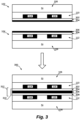
- Fig. 3 shows an example that is not covered by the present invention, but is useful for understanding some aspects of the present invention: it shows a wafer-level package construction 300, in which the ultrathin dielectric layer 310 includes multiple component dielectric layers 302 & 304 and 306 & 308.
- the ultrathin dielectric layer 310 includes multiple component dielectric layers 302 & 304 and 306 & 308.
- a first set of component dielectric layers 302 & 304 is formed on one of the integrated circuit dies 102
- a second set of component dielectric layers 306 & 308 is formed on the other integrated circuit die 104.
- Each set of ultrathin dielectric layers 302 & 304 or 306 & 308 has a thickness of less than or equal to approximately 25 nanometers, for example.
- the resulting overall ultrathin dielectric layer 310 has a thickness of less than or equal to approximately 50 nanometers, for example. Symmetry in the thickness of the multiple layers is not needed.
- the capacitive interface 312 that is formed includes the ultrathin dielectric layers 302 & 304 and 306 & 308 and respective conductive areas 114 & 116 and 118 & 120 of the first and second integrated circuit dies 102 & 104, on opposing sides of the ultrathin dielectric layer 310.
- the multiple layers may be composed of different dielectric materials, such as one or more layers of silicon oxide, and one or more a layers of a high-K dielectric other than silicon oxide, such as silicon monoxide, silicon trioxide, aluminum oxide, hafnium oxide, a high-K ionic metal oxide, a hybrid oxygen-plasma-grown metal oxide & alkylphosphonic acid self-assembled monolayer (SAM), or a polymer, for example.
- different dielectric materials such as one or more layers of silicon oxide, and one or more a layers of a high-K dielectric other than silicon oxide, such as silicon monoxide, silicon trioxide, aluminum oxide, hafnium oxide, a high-K ionic metal oxide, a hybrid oxygen-plasma-grown metal oxide & alkylphosphonic acid self-assembled monolayer (SAM), or a polymer, for example.
- the multiple layers define a parallel central plane of the multiple layers and there may be a difference in the number, arrangement, thicknesses, or composition of one or more of the multiple layers on the opposite sides of the parallel central plane of the multiple layers.
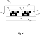
- Fig. 4 shows an example embodiment of a wafer-level package 400 including a capacitive interface 404 with an ultrathin dielectric layer 402, which can be obtained with the method of the present invention.
- the respective conductive areas 114 & 116 and 118 & 120 of the first and second integrated circuit dies 102 & 104 do not have to align perfectly on opposing sides of the ultrathin dielectric layer 402 of the capacitive interface 404.
- the respective conductive areas 114 & 116 and 118 & 120 of the first and second integrated circuit dies 102 & 104 can be staggered with respect to each other, and the staggered alignment can be used to obtain a particular capacitance, for example, between a first conductive area 114 and a second conductive area 118 on opposing sides of the capacitive interface 404.
- Fig. 5 shows an example process for making a coupled capacitive wafer-level package 500 including a capacitive interface 510.
- This process is covered by the present invention, except the variation described in paragraph [0034], which includes an additional layer 514 (illustrated on the bottom right side of Fig.5 ).
- integrated circuit dies 102 & 102' have a semiconductor 106, such as silicon, and an underfill layer 110 composed of insulation or dielectric, such as silicon dioxide, securing one or more conductive areas 114 & 116.
- Each integrated circuit die 102 & 102' has a respective surface 122 that includes the conductive areas 114 & 116. The surface 122 does not have to be flat at this point in the process.
- a layer of dielectric 502 such as silicon oxide or a high-K dielectric, is formed over the surface 122, including the one or more conductive areas 114 & 116 and exposed parts of the underfill layer 110.
- the layer of dielectric 502 is etched, lapped, or polished, to a thickness less than or equal to approximately 50 nanometers. The thickness to be achieved for a given layer of the dielectric 502 may depend on how many layers are to compose the overall ultrathin dielectric layer 508, and the value of capacitance per unit area desired.
- the layer of dielectric 502 is etched or lapped or polished down to the exposed parts of the underfill layer 110, to form a flat surface 122.
- the capacitive interface 510 resulting from the coupling includes the ultrathin dielectric layer 508, and at least one pair of conductive areas 114 & 118 or 116 & 120, on opposing sides of the ultrathin dielectric layer 508.
- a layer of etch stop 512 or a lapping-polishing stop may be applied to the initial surface 122 to protect the underlying structures and assist formation of the ultrathin dielectric layer 508 at an ultrafine pitch.
- the etch stop 512 or lapping-polishing stop is deposited on the underlying structures, such as the exposed underfill 110 and the conductive areas 114 & 116, to protect the structures (110 & 114 & 116) underlying the etch stop layer 512 from damage caused by the etch process.
- the etch stop layer 512 terminates the etch process once the desired thickness of the ultrathin dielectric layer 508 has been achieved by the etch process.
- the etch stop may be a silicon dioxide etch stop, a boron etch stop, an aluminum oxide etch stop, a polysilicon etch stop, a titanium oxide etch stop, or a silicon nitride etch stop.
- the etch or lapping process may be a dry chemical etch process, a wet etch process, a gaseous etch process, for example, using oxide etch gases such as CF 4 , CHF 3 , CH 2 F 2 , NF 3 , or O 2 , or an electrochemical etch process, e.g., using electrochemical etch rate modulation.
- the ultrathin dielectric layer 508, or a component layer thereof is formed by deposition, such as atomic layer deposition of a dielectric such as hafnium oxide (HfO 2 ).
- a combination of an oxygen-plasma-grown metal oxide (e.g., aluminum oxide) and a high-quality alkylphosphonic acid self-assembled monolayer (SAM) can be obtained at process temperatures of no more than about 100 °C, and can be formed not only on glass (silicon oxide) substrates, but also on commercially available flexible plastic substrates, such as polyethylene naphthalate or polyethylene terephthalate.
- Such an ultrathin dielectric layer 508 may have a total thickness of approximately 5-6 nanometers and a capacitance per unit area of approximately 500-800 nF/cm 2 .
- an additional ultrathin dielectric layer 514 e.g., of silicon oxide or other high-k dielectric, may be formed above the smooth flat surface 504.
- the additional ultrathin dielectric layer 514 can be used to tune the thickness, and thus the capacitance, of the resulting capacitive interface 510, once the integrated circuit dies 102 & 102' have been coupled into a stack 506, forming the capacitive interface 510.
- the additional ultrathin dielectric layer 514 can also be used to increase the resistance of the capacitive interface 510 against charge and voltage leakage, or dielectric breakdown.
- Fig. 6 shows an example method 600 of coupling integrated circuit dies or other microelectronic components. This example does not comprise all the aspects of the present invention, but is useful for understanding it. In the flow diagram, the operations are shown as individual blocks.
- integrated circuit dies are selected, each integrated circuit die having a surface that includes at least one conductive area.
- an ultrathin layer of a dielectric is formed on at least one of the surfaces of at least one of the integrated circuit dies, including at least one of the conductive areas.
- the two integrated circuit dies are coupled together in a stack to form a capacitive interface composed of the ultrathin dielectric layer and the respective conductive areas of the two integrated circuit dies on opposing sides of the ultrathin layer of the dielectric.
Landscapes
- Semiconductor Integrated Circuits (AREA)
- Internal Circuitry In Semiconductor Integrated Circuit Devices (AREA)
- Engineering & Computer Science (AREA)
- Manufacturing & Machinery (AREA)
- Chemical & Material Sciences (AREA)
- Chemical Kinetics & Catalysis (AREA)
- General Chemical & Material Sciences (AREA)
Claims (13)
- Verfahren (600) zum Koppeln von mikroelektronischen Komponenten, umfassend:Auswählen (602) von ersten und zweiten integrierten Schaltungschips (102, 102'), wobei jeder integrierte Schaltungschip (102, 102') eine Oberfläche (122) beinhaltet, die mindestens einen leitenden Bereich (114, 116, 118, 120) umfasst;Ausbilden (604) einer Schicht eines Dielektrikums (502) auf mindestens einer der Oberflächen (122) der integrierten Schaltungschips (102, 102'), wobei:die Schicht des Dielektrikums (502) über den leitenden Bereichen (114, 116, 118, 120) und über freiliegenden Teilen der mindestens einen Oberfläche (122) ausgebildet ist, unddie Schicht des Dielektrikums (502) eine Dicke von weniger als oder gleich ungefähr 50 Nanometern aufweist; undÄtzen, Läppen oder Polieren der Schicht des Dielektrikums (502) bis zu den freiliegenden Teilen der mindestens einen Oberfläche (122), um eine flache Oberfläche (122) auszubilden, die die Schicht des Dielektrikums (502) und die freiliegenden Teile der mindestens einen Oberfläche (122) umfasst; undStapeln der integrierten Schaltungschips (102, 102') durch Koppeln (606) der Oberflächen (122) und Ausbilden einer kapazitiven Schnittstelle, wobei die kapazitive Schnittstelle Folgendes umfasst:die oder jede Schicht des Dielektrikums (502, 508), undentsprechende leitende Bereiche (114, 116, 118, 120) der beiden integrierten Schaltungschips (102, 102') auf gegenüberliegenden Seiten der Schicht des Dielektrikums (508) .
- Verfahren nach Anspruch 1, wobei das Dielektrikum (502) Siliziumoxid umfasst.
- Verfahren nach Anspruch 1, wobei das Dielektrikum (502) ausgewählt ist aus der Gruppe bestehend aus Siliziumdioxid, Siliziummonoxid, Siliziumtrioxid, Aluminiumoxid, Hafniumoxid, einem hoch-κ-ionischen Metalloxid, einer hybriden sauerstoffplasmagewachsenen Metalloxid- & Alkylphosphonsäure-selbstorganisierenden Monoschicht, SAM, einem Polymerfilm und einer ionischen Metalloxidmembran.
- Verfahren nach Anspruch 3, wobei Ausbilden der Schicht des Dielektrikums (502) eine Atomschichtabscheidung von Hafniumoxid mit einer präzisen Steuerung einer Dicke des Dielektrikums bis runter auf 1-2 Nanometer umfasst.
- Verfahren nach Anspruch 3, wobei Ausbilden der Schicht des Dielektrikums (502) Erstellen einer Schicht von der Metalloxid-& Alkylphosphonsäure-selbstorganisierenden Monoschicht, SAM, umfasst, die eine Dicke von ungefähr 5-6 Nanometern und eine Kapazität pro Einheitsbereich von ungefähr 500-800 nF/cm2 aufweist.
- Verfahren nach Anspruch 1, ferner umfassend:vor dem Ausbilden der Schicht des Dielektrikums, Auftragen einer Beschichtung aus einem Ätzstopp oder einem Läpp-Polierstopp auf die mindestens eine Oberfläche;Ausbilden der Schicht des Dielektrikums (502) auf der Oberfläche; undÄtzen oder Läppen der Schicht des Dielektrikums (502), wobei der Ätzstopp oder der Läppstop eine Dicke der Schicht des Dielektrikums (502) genau steuert und unterliegende Strukturen vor dem Ätzen oder Läppen schützt.
- Verfahren nach Anspruch 6, wobei der Ätzstopp ausgewählt ist aus der Gruppe bestehend aus einem Siliziumdioxid-Ätzstopp, einem Bor-Ätzstopp, einem Aluminiumoxid-Ätzstopp, einem Polysilizium-Ätzstopp, einem Titanoxid-Ätzstopp und einem Siliziumnitrid-Ätzstopp.
- Verfahren nach Anspruch 1, ferner umfassend Ausbilden mehrerer Schichten eines Dielektrikums auf mindestens einer der Oberflächen (122) der integrierten Schaltungschips (102, 102'), wobei die mehreren Schichten des Dielektrikums eine Dicke von weniger als ungefähr 50 Nanometern umfassen.
- Verfahren nach Anspruch 8, wobei die mehreren Schichten des Dielektrikums mindestens eine Schicht aus Siliziumoxid und eine Schicht aus einem anderen hoch-κ-Dielektrikum als Siliziumoxid umfassen.
- Verfahren nach Anspruch 8, wobei die mehreren Schichten des Dielektrikums eine parallele Zentralebene der mehreren Schichten definieren und ein Unterschied in einer Anzahl, einer Anordnung, einer Dicke oder einer Zusammensetzung einer oder mehrerer der Schichten auf den gegenüberliegenden Seiten der parallelen Zentralebene der mehreren Schichten besteht.
- Verfahren nach Anspruch 1, wobei die Schicht des Dielektrikums (502) auf der mindestens einen Oberfläche der integrierten Schaltungschips (102, 102') eine Schicht umfasst, die in der Lage ist, die integrierten Schaltungschips (102, 102') aneinander zu kleben.
- Verfahren nach Anspruch 1, wobei Koppeln der integrierten Schaltungschips (102, 102') zusammen in einem Stapel mechanisches Befestigen der integrierten Schaltungschips (102, 102') zusammen an einem Rand des Stapels beinhaltet.
- Verfahren nach Anspruch 1, ferner umfassend Anordnen von Stromversorgungs- und Erdungsanschlüssen zwischen den integrierten Schaltungschips (102, 102') an einer Kante des Stapels.
Priority Applications (1)
| Application Number | Priority Date | Filing Date | Title |
|---|---|---|---|
| EP24185843.0A EP4465350A3 (de) | 2015-09-28 | 2016-08-26 | Kapazitive kopplung von komponenten integrierter schaltungen |
Applications Claiming Priority (3)
| Application Number | Priority Date | Filing Date | Title |
|---|---|---|---|
| US201562234022P | 2015-09-28 | 2015-09-28 | |
| US15/247,705 US10032751B2 (en) | 2015-09-28 | 2016-08-25 | Ultrathin layer for forming a capacitive interface between joined integrated circuit components |
| PCT/US2016/048889 WO2017058422A1 (en) | 2015-09-28 | 2016-08-26 | Capacitive coupling of integrated circuit die components |
Related Child Applications (2)
| Application Number | Title | Priority Date | Filing Date |
|---|---|---|---|
| EP24185843.0A Division EP4465350A3 (de) | 2015-09-28 | 2016-08-26 | Kapazitive kopplung von komponenten integrierter schaltungen |
| EP24185843.0A Division-Into EP4465350A3 (de) | 2015-09-28 | 2016-08-26 | Kapazitive kopplung von komponenten integrierter schaltungen |
Publications (3)
| Publication Number | Publication Date |
|---|---|
| EP3357086A1 EP3357086A1 (de) | 2018-08-08 |
| EP3357086A4 EP3357086A4 (de) | 2019-07-03 |
| EP3357086B1 true EP3357086B1 (de) | 2024-08-07 |
Family
ID=58406791
Family Applications (2)
| Application Number | Title | Priority Date | Filing Date |
|---|---|---|---|
| EP24185843.0A Pending EP4465350A3 (de) | 2015-09-28 | 2016-08-26 | Kapazitive kopplung von komponenten integrierter schaltungen |
| EP16852270.4A Active EP3357086B1 (de) | 2015-09-28 | 2016-08-26 | Verfahren zur kapazitiver kopplung von chipkomponenten einer integrierten schaltung |
Family Applications Before (1)
| Application Number | Title | Priority Date | Filing Date |
|---|---|---|---|
| EP24185843.0A Pending EP4465350A3 (de) | 2015-09-28 | 2016-08-26 | Kapazitive kopplung von komponenten integrierter schaltungen |
Country Status (6)
| Country | Link |
|---|---|
| US (2) | US10032751B2 (de) |
| EP (2) | EP4465350A3 (de) |
| KR (1) | KR102428605B1 (de) |
| CN (1) | CN108028246B (de) |
| TW (1) | TW201721745A (de) |
| WO (1) | WO2017058422A1 (de) |
Families Citing this family (36)
| Publication number | Priority date | Publication date | Assignee | Title |
|---|---|---|---|---|
| US11069734B2 (en) | 2014-12-11 | 2021-07-20 | Invensas Corporation | Image sensor device |
| US9741620B2 (en) | 2015-06-24 | 2017-08-22 | Invensas Corporation | Structures and methods for reliable packages |
| US10032751B2 (en) | 2015-09-28 | 2018-07-24 | Invensas Corporation | Ultrathin layer for forming a capacitive interface between joined integrated circuit components |
| US10811388B2 (en) | 2015-09-28 | 2020-10-20 | Invensas Corporation | Capacitive coupling in a direct-bonded interface for microelectronic devices |
| US9853037B2 (en) * | 2015-11-23 | 2017-12-26 | Micron Technology, Inc. | Integrated assemblies |
| US10204893B2 (en) | 2016-05-19 | 2019-02-12 | Invensas Bonding Technologies, Inc. | Stacked dies and methods for forming bonded structures |
| CN117878055A (zh) | 2016-12-28 | 2024-04-12 | 艾德亚半导体接合科技有限公司 | 堆栈基板的处理 |
| US10304804B2 (en) * | 2017-03-31 | 2019-05-28 | Intel Corporation | System on package architecture including structures on die back side |
| US10304686B2 (en) * | 2017-03-31 | 2019-05-28 | Intel Corporation | Electronic devices with components formed by late binding using self-assembled monolayers |
| US10879212B2 (en) * | 2017-05-11 | 2020-12-29 | Invensas Bonding Technologies, Inc. | Processed stacked dies |
| US10217720B2 (en) | 2017-06-15 | 2019-02-26 | Invensas Corporation | Multi-chip modules formed using wafer-level processing of a reconstitute wafer |
| US10134712B1 (en) | 2017-08-23 | 2018-11-20 | Micron Technology, Inc. | Methods and systems for improving power delivery and signaling in stacked semiconductor devices |
| CN111344861B (zh) | 2017-09-29 | 2026-02-03 | 英特尔公司 | 具有集成管芯附接膜的电源增强堆叠芯片级封装方案 |
| US10964664B2 (en) * | 2018-04-20 | 2021-03-30 | Invensas Bonding Technologies, Inc. | DBI to Si bonding for simplified handle wafer |
| US11276676B2 (en) | 2018-05-15 | 2022-03-15 | Invensas Bonding Technologies, Inc. | Stacked devices and methods of fabrication |
| WO2020010265A1 (en) | 2018-07-06 | 2020-01-09 | Invensas Bonding Technologies, Inc. | Microelectronic assemblies |
| WO2020010136A1 (en) | 2018-07-06 | 2020-01-09 | Invensas Bonding Technologies, Inc. | Molded direct bonded and interconnected stack |
| CN110875232A (zh) * | 2018-09-04 | 2020-03-10 | 中芯集成电路(宁波)有限公司 | 晶圆级封装方法及封装结构 |
| CN110875268A (zh) * | 2018-09-04 | 2020-03-10 | 中芯集成电路(宁波)有限公司 | 晶圆级封装方法及封装结构 |
| CN110875192A (zh) * | 2018-09-04 | 2020-03-10 | 中芯集成电路(宁波)有限公司 | 晶圆级封装方法及封装结构 |
| JP2021535613A (ja) | 2018-09-04 | 2021-12-16 | 中芯集成電路(寧波)有限公司 | ウェハレベルパッケージ方法及びパッケージ構造 |
| CN110875231A (zh) * | 2018-09-04 | 2020-03-10 | 中芯集成电路(宁波)有限公司 | 晶圆级封装方法及封装结构 |
| JP7307355B2 (ja) * | 2018-09-28 | 2023-07-12 | 株式会社ソシオネクスト | 半導体集積回路装置および半導体パッケージ構造 |
| CN119208304A (zh) * | 2018-12-06 | 2024-12-27 | 伊文萨思公司 | 用于微电子器件的直接接合的界面中的电容性耦合 |
| CN113330557A (zh) | 2019-01-14 | 2021-08-31 | 伊文萨思粘合技术公司 | 键合结构 |
| US11296053B2 (en) | 2019-06-26 | 2022-04-05 | Invensas Bonding Technologies, Inc. | Direct bonded stack structures for increased reliability and improved yield in microelectronics |
| US12080672B2 (en) | 2019-09-26 | 2024-09-03 | Adeia Semiconductor Bonding Technologies Inc. | Direct gang bonding methods including directly bonding first element to second element to form bonded structure without adhesive |
| CN112838005A (zh) * | 2019-11-25 | 2021-05-25 | 格科微电子(上海)有限公司 | 用于混合键合的晶圆表面处理方法 |
| TWI871421B (zh) * | 2020-02-03 | 2025-02-01 | 荷蘭商Asm Ip私人控股有限公司 | 包括釩或銦層的裝置、結構及其形成方法、系統 |
| US11631647B2 (en) | 2020-06-30 | 2023-04-18 | Adeia Semiconductor Bonding Technologies Inc. | Integrated device packages with integrated device die and dummy element |
| US11764177B2 (en) | 2020-09-04 | 2023-09-19 | Adeia Semiconductor Bonding Technologies Inc. | Bonded structure with interconnect structure |
| US11728273B2 (en) | 2020-09-04 | 2023-08-15 | Adeia Semiconductor Bonding Technologies Inc. | Bonded structure with interconnect structure |
| EP4315398A4 (de) | 2021-03-31 | 2025-03-05 | Adeia Semiconductor Bonding Technologies Inc. | Direktes kleben und ablösen eines trägers |
| US12094849B2 (en) * | 2021-07-22 | 2024-09-17 | Taiwan Semiconductor Manufacturing Company, Ltd. | Atomic layer deposition bonding layer for joining two semiconductor devices |
| WO2023136170A1 (ja) * | 2022-01-17 | 2023-07-20 | ソニーセミコンダクタソリューションズ株式会社 | 半導体素子及び半導体装置 |
| KR20240077946A (ko) | 2022-11-25 | 2024-06-03 | 에스케이하이닉스 주식회사 | 본딩 패드를 포함하는 반도체 장치 |
Citations (1)
| Publication number | Priority date | Publication date | Assignee | Title |
|---|---|---|---|---|
| US20050077546A1 (en) * | 2003-10-13 | 2005-04-14 | Philip Neaves | Structure and method for forming a capacitively coupled chip-to-chip signaling interface |
Family Cites Families (23)
| Publication number | Priority date | Publication date | Assignee | Title |
|---|---|---|---|---|
| US5786979A (en) * | 1995-12-18 | 1998-07-28 | Douglass; Barry G. | High density inter-chip connections by electromagnetic coupling |
| US7335995B2 (en) | 2001-10-09 | 2008-02-26 | Tessera, Inc. | Microelectronic assembly having array including passive elements and interconnects |
| DE10219116A1 (de) * | 2002-04-29 | 2003-11-13 | Infineon Technologies Ag | Integrierte Schaltungsanordnung mit Verbindungslagen sowie zugehörige Herstellungsverfahren |
| JP2003332448A (ja) * | 2002-05-14 | 2003-11-21 | Mitsubishi Electric Corp | 半導体装置 |
| US7038324B2 (en) * | 2004-03-31 | 2006-05-02 | Intel Corporation | Wafer stacking using interconnect structures of substantially uniform height |
| US7596842B2 (en) | 2005-02-22 | 2009-10-06 | Oak-Mitsui Inc. | Method of making multilayered construction for use in resistors and capacitors |
| US20060234405A1 (en) * | 2005-04-13 | 2006-10-19 | Best Scott C | Semiconductor device with self-aligning contactless interface |
| US7535105B2 (en) * | 2005-08-02 | 2009-05-19 | International Business Machines Corporation | Inter-chip ESD protection structure for high speed and high frequency devices |
| US7393736B2 (en) * | 2005-08-29 | 2008-07-01 | Micron Technology, Inc. | Atomic layer deposition of Zrx Hfy Sn1-x-y O2 films as high k gate dielectrics |
| US20080116584A1 (en) * | 2006-11-21 | 2008-05-22 | Arkalgud Sitaram | Self-aligned through vias for chip stacking |
| KR100881182B1 (ko) | 2006-11-21 | 2009-02-05 | 삼성전자주식회사 | 웨이퍼 사이에 형성된 디커플링 커패시터, 그 디커플링커패시터를 포함하는 웨이퍼 스택 패키지, 및 그 패키지제조 방법 |
| US9064936B2 (en) * | 2008-12-12 | 2015-06-23 | Stats Chippac, Ltd. | Semiconductor device and method of forming a vertical interconnect structure for 3-D FO-WLCSP |
| US8310061B2 (en) | 2008-12-17 | 2012-11-13 | Qualcomm Incorporated | Stacked die parallel plate capacitor |
| KR101046394B1 (ko) | 2010-02-03 | 2011-07-05 | 주식회사 하이닉스반도체 | 스택 패키지 |
| US8293658B2 (en) * | 2010-02-17 | 2012-10-23 | Asm America, Inc. | Reactive site deactivation against vapor deposition |
| CN104011866B (zh) * | 2011-07-27 | 2017-06-09 | 伊利诺伊大学评议会 | 用于生物分子表征的纳米孔传感器 |
| US9269612B2 (en) * | 2011-11-22 | 2016-02-23 | Taiwan Semiconductor Manufacturing Company, Ltd. | Mechanisms of forming damascene interconnect structures |
| US9142517B2 (en) * | 2012-06-05 | 2015-09-22 | Taiwan Semiconductor Manufacturing Company, Ltd. | Hybrid bonding mechanisms for semiconductor wafers |
| WO2014184988A1 (ja) | 2013-05-16 | 2014-11-20 | パナソニックIpマネジメント株式会社 | 半導体装置及びその製造方法 |
| EP2889900B1 (de) * | 2013-12-19 | 2019-11-06 | IMEC vzw | Verfahren zur Ausrichtung mikroelektronischer Bauelemente mittels Ausrichtungsflüssigkeit und elektrostatischer Ausrichtung sowie entsprechende Anordnung ausgerichteter mikroelektronischer Bauelemente |
| US9953941B2 (en) | 2015-08-25 | 2018-04-24 | Invensas Bonding Technologies, Inc. | Conductive barrier direct hybrid bonding |
| US10032751B2 (en) | 2015-09-28 | 2018-07-24 | Invensas Corporation | Ultrathin layer for forming a capacitive interface between joined integrated circuit components |
| US10141392B2 (en) | 2017-02-23 | 2018-11-27 | International Business Machines Corporation | Microstructure modulation for 3D bonded semiconductor structure with an embedded capacitor |
-
2016
- 2016-08-25 US US15/247,705 patent/US10032751B2/en active Active
- 2016-08-26 KR KR1020187011403A patent/KR102428605B1/ko active Active
- 2016-08-26 CN CN201680056319.3A patent/CN108028246B/zh active Active
- 2016-08-26 WO PCT/US2016/048889 patent/WO2017058422A1/en not_active Ceased
- 2016-08-26 EP EP24185843.0A patent/EP4465350A3/de active Pending
- 2016-08-26 EP EP16852270.4A patent/EP3357086B1/de active Active
- 2016-09-26 TW TW105131025A patent/TW201721745A/zh unknown
-
2018
- 2018-06-27 US US16/020,654 patent/US10600760B2/en active Active
Patent Citations (1)
| Publication number | Priority date | Publication date | Assignee | Title |
|---|---|---|---|---|
| US20050077546A1 (en) * | 2003-10-13 | 2005-04-14 | Philip Neaves | Structure and method for forming a capacitively coupled chip-to-chip signaling interface |
Also Published As
| Publication number | Publication date |
|---|---|
| CN108028246B (zh) | 2022-03-29 |
| WO2017058422A1 (en) | 2017-04-06 |
| KR102428605B1 (ko) | 2022-08-02 |
| US20170092620A1 (en) | 2017-03-30 |
| EP4465350A2 (de) | 2024-11-20 |
| TW201721745A (zh) | 2017-06-16 |
| US10600760B2 (en) | 2020-03-24 |
| US20180366446A1 (en) | 2018-12-20 |
| CN108028246A (zh) | 2018-05-11 |
| EP4465350A3 (de) | 2025-03-05 |
| US10032751B2 (en) | 2018-07-24 |
| KR20180049134A (ko) | 2018-05-10 |
| EP3357086A4 (de) | 2019-07-03 |
| EP3357086A1 (de) | 2018-08-08 |
Similar Documents
| Publication | Publication Date | Title |
|---|---|---|
| US10600760B2 (en) | Ultrathin layer for forming a capacitive interface between joined integrated circuit component | |
| US12272673B2 (en) | Capacitive coupling in a direct-bonded interface for microelectronic devices | |
| US11456278B2 (en) | Methods for fabricating 3D semiconductor device packages, resulting packages and systems incorporating such packages | |
| US12080672B2 (en) | Direct gang bonding methods including directly bonding first element to second element to form bonded structure without adhesive | |
| CN119208304A (zh) | 用于微电子器件的直接接合的界面中的电容性耦合 | |
| US20040235234A1 (en) | Semiconductor device and method of manufacturing the same | |
| EP2720236B1 (de) | Hochspannungsvorrichtung mit integriertem Metallkondensator und Herstellungsverfahren | |
| CN105448862A (zh) | 半导体结构及其制作方法 | |
| US20200294908A1 (en) | Bonded structures with integrated passive component | |
| US20240381034A1 (en) | Top notch slit profile for mems device | |
| CN104022073B (zh) | 微电子器件的制造方法 | |
| US20080217791A1 (en) | Semiconductor device | |
| CN106800273A (zh) | 一种在基片背面形成标记的方法 | |
| CN106032267B (zh) | 一种mems器件及其制作方法和电子装置 | |
| US8026111B2 (en) | Dielectric enhancements to chip-to-chip capacitive proximity communication | |
| KR101281240B1 (ko) | 면상 적층을 통한 패키지 테스트용 테스트 소켓의 제조방법 | |
| Jouve et al. | WSS and ZoneBOND temporary bonding techniques comparison for 80μm and 55μm functional interposer creation | |
| EP4283693B1 (de) | Grabenkondensatoren | |
| CN112201573B (zh) | 多层晶圆键合方法 | |
| CN119480869A (zh) | 半导体器件、半导体器件制作方法、存储器及存储系统 | |
| CN120826154A (zh) | 电容隔离器及其形成方法 | |
| CN110245629A (zh) | 电子装置及其制造方法 |
Legal Events
| Date | Code | Title | Description |
|---|---|---|---|
| STAA | Information on the status of an ep patent application or granted ep patent |
Free format text: STATUS: THE INTERNATIONAL PUBLICATION HAS BEEN MADE |
|
| PUAI | Public reference made under article 153(3) epc to a published international application that has entered the european phase |
Free format text: ORIGINAL CODE: 0009012 |
|
| STAA | Information on the status of an ep patent application or granted ep patent |
Free format text: STATUS: REQUEST FOR EXAMINATION WAS MADE |
|
| 17P | Request for examination filed |
Effective date: 20180323 |
|
| AK | Designated contracting states |
Kind code of ref document: A1 Designated state(s): AL AT BE BG CH CY CZ DE DK EE ES FI FR GB GR HR HU IE IS IT LI LT LU LV MC MK MT NL NO PL PT RO RS SE SI SK SM TR |
|
| AX | Request for extension of the european patent |
Extension state: BA ME |
|
| DAV | Request for validation of the european patent (deleted) | ||
| DAX | Request for extension of the european patent (deleted) | ||
| REG | Reference to a national code |
Ref country code: DE Ref legal event code: R079 Free format text: PREVIOUS MAIN CLASS: H01L0023522000 Ipc: H01L0023640000 |
|
| A4 | Supplementary search report drawn up and despatched |
Effective date: 20190603 |
|
| RIC1 | Information provided on ipc code assigned before grant |
Ipc: H01L 23/64 20060101AFI20190527BHEP Ipc: H01L 23/50 20060101ALN20190527BHEP Ipc: H01L 25/065 20060101ALN20190527BHEP Ipc: H01L 23/48 20060101ALI20190527BHEP |
|
| STAA | Information on the status of an ep patent application or granted ep patent |
Free format text: STATUS: EXAMINATION IS IN PROGRESS |
|
| 17Q | First examination report despatched |
Effective date: 20210303 |
|
| RAP1 | Party data changed (applicant data changed or rights of an application transferred) |
Owner name: ADEIA SEMICONDUCTOR TECHNOLOGIES LLC |
|
| RIC1 | Information provided on ipc code assigned before grant |
Ipc: H01L 21/60 20060101ALN20240125BHEP Ipc: H01L 21/98 20060101ALN20240125BHEP Ipc: H01L 25/065 20060101ALN20240125BHEP Ipc: H01L 23/50 20060101ALN20240125BHEP Ipc: H01L 23/48 20060101ALI20240125BHEP Ipc: H01L 23/64 20060101AFI20240125BHEP |
|
| GRAP | Despatch of communication of intention to grant a patent |
Free format text: ORIGINAL CODE: EPIDOSNIGR1 |
|
| STAA | Information on the status of an ep patent application or granted ep patent |
Free format text: STATUS: GRANT OF PATENT IS INTENDED |
|
| INTG | Intention to grant announced |
Effective date: 20240301 |
|
| RIC1 | Information provided on ipc code assigned before grant |
Ipc: H01L 21/60 20060101ALN20240220BHEP Ipc: H01L 21/98 20060101ALN20240220BHEP Ipc: H01L 25/065 20060101ALN20240220BHEP Ipc: H01L 23/50 20060101ALN20240220BHEP Ipc: H01L 23/48 20060101ALI20240220BHEP Ipc: H01L 23/64 20060101AFI20240220BHEP |
|
| GRAS | Grant fee paid |
Free format text: ORIGINAL CODE: EPIDOSNIGR3 |
|
| GRAA | (expected) grant |
Free format text: ORIGINAL CODE: 0009210 |
|
| STAA | Information on the status of an ep patent application or granted ep patent |
Free format text: STATUS: THE PATENT HAS BEEN GRANTED |
|
| AK | Designated contracting states |
Kind code of ref document: B1 Designated state(s): AL AT BE BG CH CY CZ DE DK EE ES FI FR GB GR HR HU IE IS IT LI LT LU LV MC MK MT NL NO PL PT RO RS SE SI SK SM TR |
|
| REG | Reference to a national code |
Ref country code: GB Ref legal event code: FG4D |
|
| REG | Reference to a national code |
Ref country code: CH Ref legal event code: EP |
|
| REG | Reference to a national code |
Ref country code: IE Ref legal event code: FG4D |
|
| REG | Reference to a national code |
Ref country code: DE Ref legal event code: R096 Ref document number: 602016088818 Country of ref document: DE |
|
| P01 | Opt-out of the competence of the unified patent court (upc) registered |
Free format text: CASE NUMBER: APP_45348/2024 Effective date: 20240806 |
|
| REG | Reference to a national code |
Ref country code: NL Ref legal event code: FP |
|
| REG | Reference to a national code |
Ref country code: LT Ref legal event code: MG9D |
|
| PG25 | Lapsed in a contracting state [announced via postgrant information from national office to epo] |
Ref country code: NO Free format text: LAPSE BECAUSE OF FAILURE TO SUBMIT A TRANSLATION OF THE DESCRIPTION OR TO PAY THE FEE WITHIN THE PRESCRIBED TIME-LIMIT Effective date: 20241107 |
|
| REG | Reference to a national code |
Ref country code: AT Ref legal event code: MK05 Ref document number: 1711938 Country of ref document: AT Kind code of ref document: T Effective date: 20240807 |
|
| PG25 | Lapsed in a contracting state [announced via postgrant information from national office to epo] |
Ref country code: FI Free format text: LAPSE BECAUSE OF FAILURE TO SUBMIT A TRANSLATION OF THE DESCRIPTION OR TO PAY THE FEE WITHIN THE PRESCRIBED TIME-LIMIT Effective date: 20240807 Ref country code: GR Free format text: LAPSE BECAUSE OF FAILURE TO SUBMIT A TRANSLATION OF THE DESCRIPTION OR TO PAY THE FEE WITHIN THE PRESCRIBED TIME-LIMIT Effective date: 20241108 Ref country code: PT Free format text: LAPSE BECAUSE OF FAILURE TO SUBMIT A TRANSLATION OF THE DESCRIPTION OR TO PAY THE FEE WITHIN THE PRESCRIBED TIME-LIMIT Effective date: 20241209 Ref country code: PL Free format text: LAPSE BECAUSE OF FAILURE TO SUBMIT A TRANSLATION OF THE DESCRIPTION OR TO PAY THE FEE WITHIN THE PRESCRIBED TIME-LIMIT Effective date: 20240807 |
|
| PG25 | Lapsed in a contracting state [announced via postgrant information from national office to epo] |
Ref country code: BG Free format text: LAPSE BECAUSE OF FAILURE TO SUBMIT A TRANSLATION OF THE DESCRIPTION OR TO PAY THE FEE WITHIN THE PRESCRIBED TIME-LIMIT Effective date: 20240807 |
|
| PG25 | Lapsed in a contracting state [announced via postgrant information from national office to epo] |
Ref country code: LV Free format text: LAPSE BECAUSE OF FAILURE TO SUBMIT A TRANSLATION OF THE DESCRIPTION OR TO PAY THE FEE WITHIN THE PRESCRIBED TIME-LIMIT Effective date: 20240807 |
|
| PG25 | Lapsed in a contracting state [announced via postgrant information from national office to epo] |
Ref country code: AT Free format text: LAPSE BECAUSE OF FAILURE TO SUBMIT A TRANSLATION OF THE DESCRIPTION OR TO PAY THE FEE WITHIN THE PRESCRIBED TIME-LIMIT Effective date: 20240807 Ref country code: IS Free format text: LAPSE BECAUSE OF FAILURE TO SUBMIT A TRANSLATION OF THE DESCRIPTION OR TO PAY THE FEE WITHIN THE PRESCRIBED TIME-LIMIT Effective date: 20241207 |
|
| PG25 | Lapsed in a contracting state [announced via postgrant information from national office to epo] |
Ref country code: HR Free format text: LAPSE BECAUSE OF FAILURE TO SUBMIT A TRANSLATION OF THE DESCRIPTION OR TO PAY THE FEE WITHIN THE PRESCRIBED TIME-LIMIT Effective date: 20240807 |
|
| PG25 | Lapsed in a contracting state [announced via postgrant information from national office to epo] |
Ref country code: RS Free format text: LAPSE BECAUSE OF FAILURE TO SUBMIT A TRANSLATION OF THE DESCRIPTION OR TO PAY THE FEE WITHIN THE PRESCRIBED TIME-LIMIT Effective date: 20241107 Ref country code: ES Free format text: LAPSE BECAUSE OF FAILURE TO SUBMIT A TRANSLATION OF THE DESCRIPTION OR TO PAY THE FEE WITHIN THE PRESCRIBED TIME-LIMIT Effective date: 20240807 |
|
| PG25 | Lapsed in a contracting state [announced via postgrant information from national office to epo] |
Ref country code: RS Free format text: LAPSE BECAUSE OF FAILURE TO SUBMIT A TRANSLATION OF THE DESCRIPTION OR TO PAY THE FEE WITHIN THE PRESCRIBED TIME-LIMIT Effective date: 20241107 Ref country code: PT Free format text: LAPSE BECAUSE OF FAILURE TO SUBMIT A TRANSLATION OF THE DESCRIPTION OR TO PAY THE FEE WITHIN THE PRESCRIBED TIME-LIMIT Effective date: 20241209 Ref country code: PL Free format text: LAPSE BECAUSE OF FAILURE TO SUBMIT A TRANSLATION OF THE DESCRIPTION OR TO PAY THE FEE WITHIN THE PRESCRIBED TIME-LIMIT Effective date: 20240807 Ref country code: NO Free format text: LAPSE BECAUSE OF FAILURE TO SUBMIT A TRANSLATION OF THE DESCRIPTION OR TO PAY THE FEE WITHIN THE PRESCRIBED TIME-LIMIT Effective date: 20241107 Ref country code: LV Free format text: LAPSE BECAUSE OF FAILURE TO SUBMIT A TRANSLATION OF THE DESCRIPTION OR TO PAY THE FEE WITHIN THE PRESCRIBED TIME-LIMIT Effective date: 20240807 Ref country code: IS Free format text: LAPSE BECAUSE OF FAILURE TO SUBMIT A TRANSLATION OF THE DESCRIPTION OR TO PAY THE FEE WITHIN THE PRESCRIBED TIME-LIMIT Effective date: 20241207 Ref country code: HR Free format text: LAPSE BECAUSE OF FAILURE TO SUBMIT A TRANSLATION OF THE DESCRIPTION OR TO PAY THE FEE WITHIN THE PRESCRIBED TIME-LIMIT Effective date: 20240807 Ref country code: GR Free format text: LAPSE BECAUSE OF FAILURE TO SUBMIT A TRANSLATION OF THE DESCRIPTION OR TO PAY THE FEE WITHIN THE PRESCRIBED TIME-LIMIT Effective date: 20241108 Ref country code: FI Free format text: LAPSE BECAUSE OF FAILURE TO SUBMIT A TRANSLATION OF THE DESCRIPTION OR TO PAY THE FEE WITHIN THE PRESCRIBED TIME-LIMIT Effective date: 20240807 Ref country code: ES Free format text: LAPSE BECAUSE OF FAILURE TO SUBMIT A TRANSLATION OF THE DESCRIPTION OR TO PAY THE FEE WITHIN THE PRESCRIBED TIME-LIMIT Effective date: 20240807 Ref country code: BG Free format text: LAPSE BECAUSE OF FAILURE TO SUBMIT A TRANSLATION OF THE DESCRIPTION OR TO PAY THE FEE WITHIN THE PRESCRIBED TIME-LIMIT Effective date: 20240807 Ref country code: AT Free format text: LAPSE BECAUSE OF FAILURE TO SUBMIT A TRANSLATION OF THE DESCRIPTION OR TO PAY THE FEE WITHIN THE PRESCRIBED TIME-LIMIT Effective date: 20240807 |
|
| REG | Reference to a national code |
Ref country code: CH Ref legal event code: PL |
|
| PG25 | Lapsed in a contracting state [announced via postgrant information from national office to epo] |
Ref country code: RO Free format text: LAPSE BECAUSE OF FAILURE TO SUBMIT A TRANSLATION OF THE DESCRIPTION OR TO PAY THE FEE WITHIN THE PRESCRIBED TIME-LIMIT Effective date: 20240807 Ref country code: DK Free format text: LAPSE BECAUSE OF FAILURE TO SUBMIT A TRANSLATION OF THE DESCRIPTION OR TO PAY THE FEE WITHIN THE PRESCRIBED TIME-LIMIT Effective date: 20240807 Ref country code: SM Free format text: LAPSE BECAUSE OF FAILURE TO SUBMIT A TRANSLATION OF THE DESCRIPTION OR TO PAY THE FEE WITHIN THE PRESCRIBED TIME-LIMIT Effective date: 20240807 |
|
| PG25 | Lapsed in a contracting state [announced via postgrant information from national office to epo] |
Ref country code: LU Free format text: LAPSE BECAUSE OF NON-PAYMENT OF DUE FEES Effective date: 20240826 |
|
| PG25 | Lapsed in a contracting state [announced via postgrant information from national office to epo] |
Ref country code: CH Free format text: LAPSE BECAUSE OF NON-PAYMENT OF DUE FEES Effective date: 20240831 Ref country code: EE Free format text: LAPSE BECAUSE OF FAILURE TO SUBMIT A TRANSLATION OF THE DESCRIPTION OR TO PAY THE FEE WITHIN THE PRESCRIBED TIME-LIMIT Effective date: 20240807 |
|
| PG25 | Lapsed in a contracting state [announced via postgrant information from national office to epo] |
Ref country code: CZ Free format text: LAPSE BECAUSE OF FAILURE TO SUBMIT A TRANSLATION OF THE DESCRIPTION OR TO PAY THE FEE WITHIN THE PRESCRIBED TIME-LIMIT Effective date: 20240807 |
|
| PG25 | Lapsed in a contracting state [announced via postgrant information from national office to epo] |
Ref country code: SK Free format text: LAPSE BECAUSE OF FAILURE TO SUBMIT A TRANSLATION OF THE DESCRIPTION OR TO PAY THE FEE WITHIN THE PRESCRIBED TIME-LIMIT Effective date: 20240807 |
|
| REG | Reference to a national code |
Ref country code: DE Ref legal event code: R097 Ref document number: 602016088818 Country of ref document: DE |
|
| PLBE | No opposition filed within time limit |
Free format text: ORIGINAL CODE: 0009261 |
|
| STAA | Information on the status of an ep patent application or granted ep patent |
Free format text: STATUS: NO OPPOSITION FILED WITHIN TIME LIMIT |
|
| REG | Reference to a national code |
Ref country code: BE Ref legal event code: MM Effective date: 20240831 |
|
| PG25 | Lapsed in a contracting state [announced via postgrant information from national office to epo] |
Ref country code: MC Free format text: LAPSE BECAUSE OF FAILURE TO SUBMIT A TRANSLATION OF THE DESCRIPTION OR TO PAY THE FEE WITHIN THE PRESCRIBED TIME-LIMIT Effective date: 20240807 |
|
| PG25 | Lapsed in a contracting state [announced via postgrant information from national office to epo] |
Ref country code: BE Free format text: LAPSE BECAUSE OF NON-PAYMENT OF DUE FEES Effective date: 20240831 |
|
| 26N | No opposition filed |
Effective date: 20250508 |
|
| PG25 | Lapsed in a contracting state [announced via postgrant information from national office to epo] |
Ref country code: FR Free format text: LAPSE BECAUSE OF NON-PAYMENT OF DUE FEES Effective date: 20241007 |
|
| GBPC | Gb: european patent ceased through non-payment of renewal fee |
Effective date: 20241107 |
|
| PG25 | Lapsed in a contracting state [announced via postgrant information from national office to epo] |
Ref country code: IE Free format text: LAPSE BECAUSE OF NON-PAYMENT OF DUE FEES Effective date: 20240826 |
|
| PG25 | Lapsed in a contracting state [announced via postgrant information from national office to epo] |
Ref country code: SE Free format text: LAPSE BECAUSE OF FAILURE TO SUBMIT A TRANSLATION OF THE DESCRIPTION OR TO PAY THE FEE WITHIN THE PRESCRIBED TIME-LIMIT Effective date: 20240807 |
|
| PGFP | Annual fee paid to national office [announced via postgrant information from national office to epo] |
Ref country code: NL Payment date: 20250825 Year of fee payment: 10 |
|
| PGFP | Annual fee paid to national office [announced via postgrant information from national office to epo] |
Ref country code: DE Payment date: 20250827 Year of fee payment: 10 |
|
| PG25 | Lapsed in a contracting state [announced via postgrant information from national office to epo] |
Ref country code: GB Free format text: LAPSE BECAUSE OF NON-PAYMENT OF DUE FEES Effective date: 20241107 |
|
| REG | Reference to a national code |
Ref country code: DE Ref legal event code: R079 Ref document number: 602016088818 Country of ref document: DE Free format text: PREVIOUS MAIN CLASS: H01L0023640000 Ipc: H10W0044000000 |
|
| PG25 | Lapsed in a contracting state [announced via postgrant information from national office to epo] |
Ref country code: IT Free format text: LAPSE BECAUSE OF FAILURE TO SUBMIT A TRANSLATION OF THE DESCRIPTION OR TO PAY THE FEE WITHIN THE PRESCRIBED TIME-LIMIT Effective date: 20240807 Ref country code: CY Free format text: LAPSE BECAUSE OF FAILURE TO SUBMIT A TRANSLATION OF THE DESCRIPTION OR TO PAY THE FEE WITHIN THE PRESCRIBED TIME-LIMIT; INVALID AB INITIO Effective date: 20160826 |
|
| PG25 | Lapsed in a contracting state [announced via postgrant information from national office to epo] |
Ref country code: HU Free format text: LAPSE BECAUSE OF FAILURE TO SUBMIT A TRANSLATION OF THE DESCRIPTION OR TO PAY THE FEE WITHIN THE PRESCRIBED TIME-LIMIT; INVALID AB INITIO Effective date: 20160826 |