EP3343693B1 - Elektronische vorrichtung mit antenne - Google Patents
Elektronische vorrichtung mit antenne Download PDFInfo
- Publication number
- EP3343693B1 EP3343693B1 EP16873243.6A EP16873243A EP3343693B1 EP 3343693 B1 EP3343693 B1 EP 3343693B1 EP 16873243 A EP16873243 A EP 16873243A EP 3343693 B1 EP3343693 B1 EP 3343693B1
- Authority
- EP
- European Patent Office
- Prior art keywords
- housing part
- electronic device
- antenna pattern
- antenna
- conductive member
- Prior art date
- Legal status (The legal status is an assumption and is not a legal conclusion. Google has not performed a legal analysis and makes no representation as to the accuracy of the status listed.)
- Not-in-force
Links
Images


Classifications
-
- H—ELECTRICITY
- H01—ELECTRIC ELEMENTS
- H01Q—ANTENNAS, i.e. RADIO AERIALS
- H01Q1/00—Details of, or arrangements associated with, antennas
- H01Q1/12—Supports; Mounting means
- H01Q1/22—Supports; Mounting means by structural association with other equipment or articles
- H01Q1/24—Supports; Mounting means by structural association with other equipment or articles with receiving set
- H01Q1/241—Supports; Mounting means by structural association with other equipment or articles with receiving set used in mobile communications, e.g. GSM
- H01Q1/242—Supports; Mounting means by structural association with other equipment or articles with receiving set used in mobile communications, e.g. GSM specially adapted for hand-held use
- H01Q1/243—Supports; Mounting means by structural association with other equipment or articles with receiving set used in mobile communications, e.g. GSM specially adapted for hand-held use with built-in antennas
-
- H—ELECTRICITY
- H01—ELECTRIC ELEMENTS
- H01Q—ANTENNAS, i.e. RADIO AERIALS
- H01Q1/00—Details of, or arrangements associated with, antennas
- H01Q1/12—Supports; Mounting means
- H01Q1/22—Supports; Mounting means by structural association with other equipment or articles
- H01Q1/2258—Supports; Mounting means by structural association with other equipment or articles used with computer equipment
- H01Q1/2266—Supports; Mounting means by structural association with other equipment or articles used with computer equipment disposed inside the computer
-
- H—ELECTRICITY
- H01—ELECTRIC ELEMENTS
- H01Q—ANTENNAS, i.e. RADIO AERIALS
- H01Q1/00—Details of, or arrangements associated with, antennas
- H01Q1/12—Supports; Mounting means
- H01Q1/22—Supports; Mounting means by structural association with other equipment or articles
- H01Q1/24—Supports; Mounting means by structural association with other equipment or articles with receiving set
-
- H—ELECTRICITY
- H01—ELECTRIC ELEMENTS
- H01Q—ANTENNAS, i.e. RADIO AERIALS
- H01Q1/00—Details of, or arrangements associated with, antennas
- H01Q1/36—Structural form of radiating elements, e.g. cone, spiral, umbrella; Particular materials used therewith
- H01Q1/38—Structural form of radiating elements, e.g. cone, spiral, umbrella; Particular materials used therewith formed by a conductive layer on an insulating support
-
- H—ELECTRICITY
- H01—ELECTRIC ELEMENTS
- H01Q—ANTENNAS, i.e. RADIO AERIALS
- H01Q1/00—Details of, or arrangements associated with, antennas
- H01Q1/48—Earthing means; Earth screens; Counterpoises
-
- H—ELECTRICITY
- H01—ELECTRIC ELEMENTS
- H01Q—ANTENNAS, i.e. RADIO AERIALS
- H01Q21/00—Antenna arrays or systems
-
- H—ELECTRICITY
- H01—ELECTRIC ELEMENTS
- H01Q—ANTENNAS, i.e. RADIO AERIALS
- H01Q9/00—Electrically-short antennas having dimensions not more than twice the operating wavelength and consisting of conductive active radiating elements
- H01Q9/04—Resonant antennas
-
- H—ELECTRICITY
- H01—ELECTRIC ELEMENTS
- H01Q—ANTENNAS, i.e. RADIO AERIALS
- H01Q9/00—Electrically-short antennas having dimensions not more than twice the operating wavelength and consisting of conductive active radiating elements
- H01Q9/04—Resonant antennas
- H01Q9/30—Resonant antennas with feed to end of elongated active element, e.g. unipole
- H01Q9/42—Resonant antennas with feed to end of elongated active element, e.g. unipole with folded element, the folded parts being spaced apart a small fraction of the operating wavelength
-
- H—ELECTRICITY
- H04—ELECTRIC COMMUNICATION TECHNIQUE
- H04M—TELEPHONIC COMMUNICATION
- H04M1/00—Substation equipment, e.g. for use by subscribers
- H04M1/02—Constructional features of telephone sets
-
- H—ELECTRICITY
- H04—ELECTRIC COMMUNICATION TECHNIQUE
- H04M—TELEPHONIC COMMUNICATION
- H04M1/00—Substation equipment, e.g. for use by subscribers
- H04M1/02—Constructional features of telephone sets
- H04M1/0202—Portable telephone sets, e.g. cordless phones, mobile phones or bar type handsets
- H04M1/0206—Portable telephones comprising a plurality of mechanically joined movable body parts, e.g. hinged housings
- H04M1/0208—Portable telephones comprising a plurality of mechanically joined movable body parts, e.g. hinged housings characterized by the relative motions of the body parts
- H04M1/0214—Foldable telephones, i.e. with body parts pivoting to an open position around an axis parallel to the plane they define in closed position
- H04M1/0216—Foldable in one direction, i.e. using a one degree of freedom hinge
-
- H—ELECTRICITY
- H04—ELECTRIC COMMUNICATION TECHNIQUE
- H04M—TELEPHONIC COMMUNICATION
- H04M1/00—Substation equipment, e.g. for use by subscribers
- H04M1/02—Constructional features of telephone sets
- H04M1/0202—Portable telephone sets, e.g. cordless phones, mobile phones or bar type handsets
- H04M1/026—Details of the structure or mounting of specific components
- H04M1/0266—Details of the structure or mounting of specific components for a display module assembly
- H04M1/0268—Details of the structure or mounting of specific components for a display module assembly including a flexible display panel
-
- H—ELECTRICITY
- H05—ELECTRIC TECHNIQUES NOT OTHERWISE PROVIDED FOR
- H05K—PRINTED CIRCUITS; CASINGS OR CONSTRUCTIONAL DETAILS OF ELECTRIC APPARATUS; MANUFACTURE OF ASSEMBLAGES OF ELECTRICAL COMPONENTS
- H05K5/00—Casings, cabinets or drawers for electric apparatus
Definitions
- Various embodiments of the present disclosure relate to an electronic device including an antenna.
- an electronic device may be formed in a bendable structure or a foldable structure.
- an electronic device may include a flip cover, a dual display, a flexible display, and the like.
- An electronic device having a communication function can provide a mobile communication service through an antenna.
- the antenna may be disposed at a portion of the interior and/or exterior of the housing of the electronic device.
- the antenna may be formed in a pattern on a printed circuit board (PCB).
- US2003/0045246 A1 discloses an antenna for a foldable device, comprising an exposed conductive member on each of the two housing parts of the foldable device, and wherein the conductive members are each connected to an antenna pattern.
- the conductive members are configured to be connected when the foldable device is in an open state, causing the radiation pattern of the antenna to be altered.
- the antenna may be located inside the electronic device, and the housing of the electronic device may be formed of a metal frame which is a conductive material.
- a signal transmitted to the outside from the antenna located inside the electronic device may be distorted or blocked at least partially by the metal frame, thereby causing the degradation of antenna radiation performance.
- a space inside the housing of the electronic device in which the antenna is mounted may be limited. Moreover, when the electronic device is reduced in size, the space inside the housing may be further limited. In addition, when the frequency band supported by the antenna is variable, the space inside the housing may be further limited because a plurality of antennas or a complex-shaped antenna should be disposed.
- an electronic device including an antenna that is not limited to a space inside the electronic device and does not deteriorate antenna radiation performance by a conductive material.
- an electronic device may comprise a foldable housing including a first housing part including a first surface and a second surface opposite to the first surface, a second housing part including a first surface facing the first surface of the first housing part when folded in a first direction, and a second surface facing the second surface of the first housing part when folded in a second direction, and a connection part connecting the first housing part and the second housing part; a communication circuit disposed inside the housing; a first antenna pattern disposed inside the first housing part; a second antenna pattern disposed inside the second housing part; a first display exposed to the first surface of the first housing part; a second display exposed to the first surface of the second housing part; a first conductive member exposed to the second surface of the first housing part, and electrically connected to the first antenna pattern; and a second conductive member exposed to the second surface of the second housing part, and electrically connected to the second antenna pattern, wherein the communication circuit is electrically connected to the first antenna pattern and/or the second antenna pattern, and wherein the first conductive member and
- an electronic device may comprise a housing including a first surface and a second surface opposite to the first surface; a communication circuit disposed inside the housing; at least one first conductive member exposed to a portion of the second surface of the housing; at least one second conductive member exposed to another portion of the second surface of the housing; a first antenna pattern disposed inside the housing and electrically connected to the first conductive member; and a second antenna pattern disposed inside the housing and electrically connected to the second conductive member, wherein the communication circuit is electrically connected to the first antenna pattern and/or the second antenna pattern, wherein when folded in a first direction, at least a portion of the first surface meets at least another portion of the first surface, and wherein when folded in a second direction, at least a portion of the second surface meets at least another portion of the second surface, and the first conductive member and the second conductive member are electrically connected to or coupling with each other.
- an electronic device including an antenna can efficiently utilize an internal space. Further, according to various embodiments of the present disclosure, an electronic device including an antenna can maintain antenna performance without the deterioration of the antenna performance by a conductive material.
- the expression “and/or” includes any and all combinations of the associated listed words.
- the expression “A and/or B” may include A, may include B, or may include both A and B.
- expressions including ordinal numbers, such as "first”and “second,” etc. may modify various elements.
- such elements are not limited by the above expressions.
- the above expressions do not limit the sequence and/or importance of the elements.
- the above expressions are used merely for the purpose to distinguish an element from the other elements.
- a first user device and a second user device indicate different user devices although both of them are user devices.
- a first element could be termed a second element, and similarly, a second element could be also termed a first element without departing from the scope of the present disclosure.
- An electronic device may be a device including a communication function.
- the device corresponds to a combination of at least one of a smartphone, a tablet Personal Computer (PC), a mobile phone, a video phone , an e-book reader, a desktop PC, a laptop PC, a netbook computer, a Personal Digital Assistant (PDA), a Portable Multimedia Player (PMP), adigital audio player, a mobile medical device, an electronic bracelet, an electronic necklace, an electronic accessory, a camera, a wearable device, an electronic clock, a wrist watch, home appliances (for example, an air-conditioner, vacuum, an oven, a microwave, a washing machine, an air cleaner, and the like), an artificial intelligence robot, a TeleVision (TV), a Digital Video Disk (DVD) player, an audio device, various medical devices (for example, Magnetic Resonance Angiography (MRA), Magnetic Resonance Imaging (MRI), Computed Tomography (CT), a scanning machine, a ultrasonic wave device, or
- MRA Magnetic
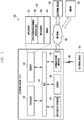
- FIG. 1 is a block diagram illustrating a configuration of an electronic device according to an embodiment of the present disclosure.
- the electronic device 100 may include a bus 110, a processor 120, a memory 130, a user input module 140, a display module 150, a communication module 160, and other similar and/or suitable components.
- the bus 110 may be a circuit which interconnects the above-described elements and delivers a communication (e.g., a control message) between the above-described elements.
- the processor 120 may receive commands from the above-described other elements (e.g., the memory 130, the user input module 140, the display module 150, the communication module 160, etc.) through the bus 110, may interpret the received commands, and may execute calculation or data processing according to the interpreted commands.
- the above-described other elements e.g., the memory 130, the user input module 140, the display module 150, the communication module 160, etc.
- the memory 130 may store commands or data received from the processor 120 or other elements (e.g., the user input module 140, the display module 150, the communication module 160, etc.) or generated by the processor 120 or the other elements.
- the memory 130 may include programming modules, such as a kernel 131, middleware 132, an Application Programming Interface (API) 133, an application 134, and the like. Each of the above-described programming modules may be implemented in software, firmware, hardware, or a combination of two or more thereof.
- the kernel 131 may control or manage system resources (e.g., the bus 110, the processor 120, the memory 130, etc.) used to execute operations or functions implemented by other programming modules (e.g., the middleware 132, the API 133, and the application 134). Also, the kernel 131 may provide an interface capable of accessing and controlling or managing the individual elements of the electronic device 100 by using the middleware 132, the API 133, or the application 134.
- system resources e.g., the bus 110, the processor 120, the memory 130, etc.
- other programming modules e.g., the middleware 132, the API 133, and the application 134.
- the kernel 131 may provide an interface capable of accessing and controlling or managing the individual elements of the electronic device 100 by using the middleware 132, the API 133, or the application 134.
- the middleware 132 may serve to go between the API 133 or the application 134 and the kernel 131 in such a manner that the API 133 or the application 134 communicates with the kernel 131 and exchanges data therewith. Also, in relation to work requests received from one or more applications 134 and/or the middleware 132, for example, may perform load balancing of the work requests by using a method of assigning a priority, in which system resources (e.g., the bus 110, the processor 120, the memory 130, etc.) of the electronic device 100 can be used, to at least one of the one or more applications 134.
- system resources e.g., the bus 110, the processor 120, the memory 130, etc.
- the API 133 is an interface through which the application 134 is capable of controlling a function provided by the kernel 131 or the middleware 132, and may include, for example, at least one interface or function for file control, window control, image processing, character control, or the like.
- the user input module 140 may receive a command or data as input from a user, and may deliver the received command or data to the processor 120 or the memory 130 through the bus 110.
- the display module 150 may display a video, an image, data, or the like to the user.
- the communication module 160 may connect communication between another electronic device 102 and the electronic device 100.
- the communication module 160 may support a predetermined short-range communication protocol (e.g., Wi-Fi, BlueTooth (BT), and Near Field Communication (NFC)), or predetermined network communication 162 (e.g., the Internet, a Local Area Network (LAN), a Wide Area Network (WAN), a telecommunication network, a cellular network, a satellite network, a Plain Old Telephone Service (POTS), or the like).
- LAN Local Area Network
- WAN Wide Area Network
- POTS Plain Old Telephone Service
- Each of the electronic devices 102 and 104 may be a device which is identical (e.g., of an identical type) to or different (e.g., of a different type) from the electronic device 100.
- the communication module 160 may connect communication between a server 164 and the electronic device 100 via the network 162.
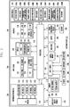
- FIG. 2 is a block diagram illustrating a configuration of hardware 200 according to an embodiment of the present disclosure.
- the hardware 200 may be, for example, the electronic device 100 illustrated in FIG. 1 .
- the hardware 200 may include one or more processors 210, a Subscriber Identification Module (SIM) card 214, a memory 220, a communication module 230, a sensor module 240, a user input module 250, a display module 260, an interface 270, an audio coder/decoder (codec) 280, a camera module 291, a power management module 295, a battery 296, an indicator 297, a motor 298 and any other similar and/or suitable components.
- SIM Subscriber Identification Module
- the processor 210 may include one or more Application Processors (APs) 211, or one or more Communication Processors (CPs) 213.
- the processor 210 may be, for example, the processor 120 illustrated in FIG. 1 .
- the AP 211 and the CP 213 are illustrated as being included in the processor 210 in FIG. 2 , but may be included in different Integrated Circuit (IC) packages, respectively. According to an embodiment of the present disclosure, the AP 211 and the CP 213 may be included in one IC package.
- the AP 211 may execute an Operating System (OS) or an application program, and thereby may control multiple hardware or software elements connected to the AP 211 and may perform processing of and arithmetic operations on various data including multimedia data.
- the AP 211 may be implemented by, for example, a System on Chip (SoC).
- SoC System on Chip
- the processor 210 may further include a Graphical Processing Unit (GPU) (not illustrated).
- GPU Graphical Processing Unit
- the CP 213 may manage a data line and may convert a communication protocol in the case of communication between the electronic device (e.g., the electronic device 100) including the hardware 200 and different electronic devices connected to the electronic device through the network.
- the CP 213 may be implemented by, for example, a SoC. According to an embodiment of the present disclosure, the CP 213 may perform at least some of multimedia control functions.
- the CP 213, for example, may distinguish and authenticate a terminal in a communication network by using a subscriber identification module (e.g., the SIM card 214). Also, the CP 213 may provide the user with services, such as a voice telephony call, a video telephony call, a text message, packet data, and the like.
- the CP 213 may control the transmission and reception of data by the communication module 230.
- the elements such as the CP 213, the power management module 295, the memory 220, and the like are illustrated as elements separate from the AP 211.
- the AP 211 may include at least some (e.g., the CP 213) of the above-described elements.
- the AP 211 or the CP 213 may load, to a volatile memory, a command or data received from at least one of a non-volatile memory and other elements connected to each of the AP 211 and the CP 213, and may process the loaded command or data. Also, the AP 211 or the CP 213 may store, in a non-volatile memory, data received from or generated by at least one of the other elements.
- the SIM card 214 may be a card implementing a subscriber identification module, and may be inserted into a slot formed in a particular portion of the electronic device 100.
- the SIM card 214 may include unique identification information (e.g., Integrated Circuit Card IDentifier (ICCID)) or subscriber information (e.g., International Mobile Subscriber Identity (IMSI)).
- ICCID Integrated Circuit Card IDentifier
- IMSI International Mobile Subscriber Identity
- the memory 220 may include an internal memory 222 and an external memory 224.
- the memory 220 may be, for example, the memory 130 illustrated in FIG. 1 .
- the internal memory 222 may include, for example, at least one of a volatile memory (e.g., a Dynamic RAM (DRAM), a Static RAM (SRAM), a Synchronous Dynamic RAM (SDRAM), etc.), and a non-volatile memory (e.g., a One Time Programmable ROM (OTPROM), a Programmable ROM (PROM), an Erasable and Programmable ROM (EPROM), an Electrically Erasable and Programmable ROM (EEPROM), a mask ROM, a flash ROM, a Not AND (NAND) flash memory, a Not OR (NOR) flash memory, etc.).
- a volatile memory e.g., a Dynamic RAM (DRAM), a Static RAM (SRAM), a Synchronous Dynamic RAM (SDRAM), etc.
- the internal memory 222 may be in the form of a Solid State Drive (SSD).
- the external memory 224 may further include a flash drive, for example, a Compact Flash (CF), a Secure Digital (SD), a Micro-Secure Digital (Micro-SD), a Mini-Secure Digital (Mini-SD), an extreme Digital (xD), a memory stick, or the like.
- CF Compact Flash
- SD Secure Digital
- Micro-SD Micro-Secure Digital
- Mini-SD Mini-Secure Digital
- xD extreme Digital
- the communication module 230 may include a wireless communication module 231 or a Radio Frequency (RF) module 234.
- the communication module 230 may be, for example, the communication module 160 illustrated in FIG. 1 .
- the wireless communication module 231 may include, for example, a Wi-Fi part 233, a BT part 235, a GPS part 237, or a NFC part 239.
- the wireless communication module 231 may provide a wireless communication function by using a radio frequency.
- the wireless communication module 231 may include a network interface (e.g., a LAN card), a modulator/demodulator (modem), or the like for connecting the hardware 200 to a network (e.g., the Internet, a LAN, a WAN, a telecommunication network, a cellular network, a satellite network, a POTS, or the like).
- a network e.g., the Internet, a LAN, a WAN, a telecommunication network, a cellular network, a satellite network, a POTS, or the like.
- the RF module 234 may be used for transmission and reception of data, for example, transmission and reception of RF signals or called electronic signals.
- the RF unit 234 may include, for example, a transceiver, a Power Amplifier Module (PAM), a frequency filter, a Low Noise Amplifier (LNA), or the like.
- the RF module 234 may further include a component for transmitting and receiving electromagnetic waves in a free space in a wireless communication, for example, a conductor, a conductive wire, or the like.
- the sensor module 240 may include, for example, at least one of a gesture sensor 240A, a gyro sensor 240B, an atmospheric pressure sensor 240C, a magnetic sensor 240D, an acceleration sensor 240E, a grip sensor 240F, a proximity sensor 240G, a Red, Green and Blue (RGB) sensor 240H, a biometric sensor 2401, a temperature/humidity sensor 240J, an illuminance sensor 240K, and a Ultra Violet (UV) sensor 240M.
- the sensor module 240 may measure a physical quantity or may sense an operating state of the electronic device 100, and may convert the measured or sensed information to an electrical signal.
- the sensor module 240 may include, for example, an E-nose sensor (not illustrated), an ElectroMyoGraphy (EMG) sensor (not illustrated), an ElectroEncephaloGram (EEG) sensor (not illustrated), an ElectroCardioGram (ECG) sensor (not illustrated), a fingerprint sensor (not illustrated), and the like. Additionally or alternatively, the sensor module 240 may include, for example, an E-nose sensor (not illustrated), an EMG sensor (not illustrated), an EEG sensor (not illustrated), an ECG sensor (not illustrated), a fingerprint sensor, and the like. The sensor module 240 may further include a control circuit (not illustrated) for controlling one or more sensors included therein.
- EMG ElectroMyoGraphy
- EEG ElectroEncephaloGram
- ECG ElectroCardioGram
- a fingerprint sensor not illustrated
- the sensor module 240 may include, for example, an E-nose sensor (not illustrated), an EMG sensor (not illustrated), an EEG sensor (not illustrated), an ECG sensor (not illustrated), a fingerprint sensor
- the user input module 250 may include a touch panel 252, a pen sensor 254 (e.g., a digital pen sensor), keys 256, and an ultrasonic input unit 258.
- the user input module 250 may be, for example, the user input module 140 illustrated in FIG. 1 .
- the touch panel 252 may recognize a touch input in at least one of, for example, a capacitive scheme, a resistive scheme, an infrared scheme, and an acoustic wave scheme.
- the touch panel 252 may further include a controller (not illustrated). In the capacitive type, the touch panel 252 is capable of recognizing proximity as well as a direct touch.
- the touch panel 252 may further include a tactile layer (not illustrated). In this event, the touch panel 252 may provide a tactile response to the user.
- the pen sensor 254 may be implemented by using a method identical or similar to a method of receiving a touch input from the user, or by using a separate sheet for recognition.
- a key pad or a touch key may be used as the keys 256.
- the ultrasonic input unit 258 enables the terminal to sense a sound wave by using a microphone (e.g., a microphone 288) of the terminal through a pen generating an ultrasonic signal, and to identify data.
- the ultrasonic input unit 258 is capable of wireless recognition.
- the hardware 200 may receive a user input from an external device (e.g., a network, a computer, or a server), which is connected to the communication module 230, through the communication module 230.
- the display module 260 may include a panel 262 or a hologram 264.
- the display module 260 may be, for example, the display module 150 illustrated in FIG. 1 .
- the panel 262 may be, for example, a Liquid Crystal Display (LCD) and an Active Matrix Organic Light Emitting Diode (AM-OLED) display, and the like.
- the panel 262 may be implemented so as to be, for example, flexible, transparent, or wearable.
- the panel 262 may include the touch panel 252 and one module.
- the hologram 264 may display a three-dimensional image in the air by using interference of light.
- the display module 260 may further include a control circuit for controlling the panel 262 or the hologram 264.
- the interface 270 may include, for example, a High-Definition Multimedia Interface (HDMI) 272, a Universal Serial Bus (USB) 274, a projector 276, and a D-subminiature (D-sub) 278. Additionally or alternatively, the interface 270 may include, for example, SD/Multi-Media Card (MMC) (not illustrated) or Infrared Data Association (IrDA) (not illustrated).
- HDMI High-Definition Multimedia Interface
- USB Universal Serial Bus
- projector 276 and a D-subminiature 278.
- D-sub D-subminiature
- the interface 270 may include, for example, SD/Multi-Media Card (MMC) (not illustrated) or Infrared Data Association (IrDA) (not illustrated).
- MMC Multi-Media Card
- IrDA Infrared Data Association
- the audio codec 280 may bidirectionally convert between a voice and an electrical signal.
- the audio codec 280 may convert voice information, which is input to or output from the audio codec 280, through, for example, a speaker 282, a receiver 284, an earphone 286, the microphone 288 or the like.
- the camera module 291 may capture an image and a moving image.
- the camera module 291 may include one or more image sensors (e.g., a front lens or a back lens), an Image Signal Processor (ISP) (not illustrated), and a flash LED (not illustrated).
- ISP Image Signal Processor
- flash LED not illustrated
- the power management module 295 may manage power of the hardware 200. Although not illustrated, the power management module 295 may include, for example, a Power Management Integrated Circuit (PMIC), a charger Integrated Circuit (IC), or a battery fuel gauge.
- PMIC Power Management Integrated Circuit
- IC charger Integrated Circuit
- battery fuel gauge a Battery Fuel gauge
- the PMIC may be mounted to, for example, an IC or a SoC semiconductor.
- Charging methods may be classified into a wired charging method and a wireless charging method.
- the charger IC may charge a battery, and may prevent an overvoltage or an overcurrent from a charger to the battery.
- the charger IC may include a charger IC for at least one of the wired charging method and the wireless charging method.
- Examples of the wireless charging method may include a magnetic resonance method, a magnetic induction method, an electromagnetic method, and the like. Additional circuits (e.g., a coil loop, a resonance circuit, a rectifier, etc.) for wireless charging may be added in order to perform the wireless charging.
- the battery fuel gauge may measure, for example, a residual quantity of the battery 296, or a voltage, a current or a temperature during the charging.
- the battery 296 may supply power by generating electricity, and may be, for example, a rechargeable battery.
- the indicator 297 may indicate particular states of the hardware 200 or a part (e.g., the AP 211) of the hardware 200, for example, a booting state, a message state, a charging state and the like.
- the motor 298 may convert an electrical signal into a mechanical vibration.
- the processor 210 may control the sensor module 240.
- the hardware 200 may include a processing unit (e.g., a GPU) for supporting a module TV.
- the processing unit for supporting a module TV may process media data according to standards such as, for example, Digital Multimedia Broadcasting (DMB), Digital Video Broadcasting (DVB), media flow, and the like.
- DMB Digital Multimedia Broadcasting
- DVD Digital Video Broadcasting
- Each of the above-described elements of the hardware 200 according to an embodiment of the present disclosure may include one or more components, and the name of the relevant element may change depending on the type of electronic device.
- the hardware 200 according to an embodiment of the present disclosure may include at least one of the above-described elements. Some of the above-described elements may be omitted from the hardware 200, or the hardware 200 may further include additional elements. Also, some of the elements of the hardware 200 according to an embodiment of the present disclosure may be combined into one entity, which may perform functions identical to those of the relevant elements before the combination.
- module used in the present disclosure may refer to, for example, a unit including one or more combinations of hardware, software, and firmware.
- the “module” may be interchangeable with a term, such as “unit,” “logic,” “logical block,” “component,” “circuit,” or the like.
- the “module” may be a minimum unit of a component formed as one body or a part thereof.
- the “module” may be a minimum unit for performing one or more functions or a part thereof.
- the “module” may be implemented mechanically or electronically.
- the "module” may include at least one of an Application-Specific Integrated Circuit (ASIC) chip, a Field-Programmable Gate Array (FPGA), and a programmable-logic device for performing certain operations which have been known or are to be developed in the future.
- ASIC Application-Specific Integrated Circuit
- FPGA Field-Programmable Gate Array
- programmable-logic device for performing certain operations which have been known or are to be developed in the future.
- FIG. 3 is a block diagram illustrating a configuration of a programming module 300 according to an embodiment of the present disclosure.
- the programming module 300 may be included (or stored) in the electronic device 100 (e.g., the memory 130) or may be included (or stored) in the electronic device 200 (e.g., the memory 230) illustrated in FIG. 1 . At least a part of the programming module 300 may be implemented in software, firmware, hardware, or a combination of two or more thereof.
- the programming module 300 may be implemented in hardware (e.g., the hardware 200), and may include an OS controlling resources related to an electronic device (e.g., the electronic device 100) and/or various applications (e.g., an application 370) executed in the OS.
- the OS may be Android, iOS, Windows, Symbian, Tizen, Bada, and the like.
- the programming module 300 may include a kernel 310, a middleware 330, an API 360, and/or the application 370.
- the kernel 310 may include a system resource manager 311 and/or a device driver 312.
- the system resource manager 311 may include, for example, a process manager (not illustrated), a memory manager (not illustrated), and a file system manager (not illustrated).
- the system resource manager 311 may perform the control, allocation, recovery, and/or the like of system resources.
- the device driver 312 may include, for example, a display driver (not illustrated), a camera driver (not illustrated), a Bluetooth driver (not illustrated), a shared memory driver (not illustrated), a USB driver (not illustrated), a keypad driver (not illustrated), a Wi-Fi driver (not illustrated), and/or an audio driver (not illustrated).
- the device driver 312 may include an Inter-Process Communication (IPC) driver (not illustrated).
- IPC Inter-Process Communication
- the middleware 330 may include multiple modules previously implemented so as to provide a function used in common by the applications 370. Also, the middleware 330 may provide a function to the applications 370 through the API 360 in order to enable the applications 370 to efficiently use limited system resources within the electronic device. For example, as illustrated in FIG.
- the middleware 330 may include at least one of a runtime library 335, an application manager 341, a window manager 342, a multimedia manager 343, a resource manager 344, a power manager 345, a database manager 346, a package manager 347, a connectivity manager 348, a notification manager 349, a location manager 350, a graphic manager 351, a security manager 352, and any other suitable and/or similar manager.
- the runtime library 335 may include, for example, a library module used by a complier, in order to add a new function by using a programming language during the execution of the application 370. According to an embodiment of the present disclosure, the runtime library 335 may perform functions which are related to input and output, the management of a memory, an arithmetic function, and/or the like.
- the application manager 341 may manage, for example, a life cycle of at least one of the applications 370.
- the window manager 342 may manage GUI resources used on the screen.
- the multimedia manager 343 may detect a format used to reproduce various media files and may encode or decode a media file through a codec appropriate for the relevant format.
- the resource manager 344 may manage resources, such as a source code, a memory, a storage space, and/or the like of at least one of the applications 370.
- the power manager 345 may operate together with a Basic Input/Output System (BIOS), may manage a battery or power, and may provide power information and the like used for an operation.
- BIOS Basic Input/Output System
- the database manager 346 may manage a database in such a manner as to enable the generation, search and/or change of the database to be used by at least one of the applications 370.
- the package manager 347 may manage the installation and/or update of an application distributed in the form of a package file.
- the connectivity manager 348 may manage a wireless connectivity such as, for example, Wi-Fi and Bluetooth.
- the notification manager 349 may display or report, to the user, an event such as an arrival message, an appointment, a proximity alarm, and the like in such a manner as not to disturb the user.
- the location manager 350 may manage location information of the electronic device.
- the graphic manager 351 may manage a graphic effect, which is to be provided to the user, and/or a user interface related to the graphic effect.
- the security manager 352 may provide various security functions used for system security, user authentication, and the like.
- the middleware 330 may further include a telephony manager (not illustrated) for managing a voice telephony call function and/or a video telephony call function of the electronic device.
- a telephony manager not illustrated for managing a voice telephony call function and/or a video telephony call function of the electronic device.
- the middleware 330 may generate and use a new middleware module through various functional combinations of the above-described internal element modules.
- the middleware 330 may provide modules specialized according to types of OSs in order to provide differentiated functions.
- the middleware 330 may dynamically delete some of the existing elements, or may add new elements. Accordingly, the middleware 330 may omit some of the elements described in the various embodiments of the present disclosure, may further include other elements, or may replace the some of the elements with elements, each of which performs a similar function and has a different name.
- the API 360 (e.g., the API 133) is a set of API programming functions, and may be provided with a different configuration according to an OS. In the case of Android or iOS, for example, one API set may be provided to each platform. In the case of Tizen, for example, two or more API sets may be provided to each platform.
- the applications 370 may include, for example, a preloaded application and/or a third party application.
- the applications 370 may include, for example, a home application 371, a dialer application 372, a Short Message Service (SMS)/Multimedia Message Service (MMS) application 373, an Instant Message (IM) application 374, a browser application 375, a camera application 376, an alarm application 377, a contact application 378, a voice dial application 379, an electronic mail (e-mail) application 380, a calendar application 381, a media player application 382, an album application 383, a clock application 384, and any other suitable and/or similar application.
- SMS Short Message Service
- MMS Multimedia Message Service
- IM Instant Message
- a browser application 375 a camera application 376
- an alarm application 377 an alarm application 377
- a contact application 378 a voice dial application 379
- an electronic mail (e-mail) application 380 a calendar application 381, a media player application
- At least a part of the programming module 300 may be implemented by instructions stored in a non-transitory computer-readable storage medium. When the instructions are executed by one or more processors (e.g., the one or more processors 210), the one or more processors may perform functions corresponding to the instructions.
- the non-transitory computer-readable storage medium may be, for example, the memory 220.
- At least a part of the programming module 300 may be implemented (e.g., executed) by, for example, the one or more processors 210.
- At least a part of the programming module 300 may include, for example, a module, a program, a routine, a set of instructions, and/or a process for performing one or more functions.
- Names of the elements of the programming module may change depending on the type of OS.
- the programming module according to an embodiment of the present disclosure may include one or more of the above-described elements. Alternatively, some of the above-described elements may be omitted from the programming module. Alternatively, the programming module may further include additional elements.
- the operations performed by the programming module or other elements according to an embodiment of the present disclosure may be processed in a sequential method, a parallel method, a repetitive method, or a heuristic method. Also, some of the operations may be omitted, or other operations may be added to the operations.
- FIG. 4 is a schematic block diagram of an electronic device according to various embodiments of the present disclosure.
- the electronic device 400 may include an antenna 410, a power management module 495, a battery 496, a communication module 420, and a processor 470.
- the electronic device 400 may be the same electronic device as the electronic device 101 of FIG. 1 and the electronic device 201 of FIG. 2 . Thus, the description of the same element will be omitted since previously described in FIG. 2 .
- the antenna 410 may be an antenna for at least one communication scheme among cellular, wireless fidelity (Wi-Fi), Bluetooth (BT), GPS, near field communication (NFC), and magnetic secure transmission (MST).
- the antenna 410 may be an antenna for wirelessly charging the battery 496.
- the antenna 410 may be a planar inverted F antenna (PIFA) or a monopole antenna, and the volume and the number of the antenna 410 may be determined depending on a service frequency, a bandwidth, a type, and the like.
- the antenna 410 typically uses a low band of 700 MHz to 900 MHz, a mid band of 1700 MHz to 2100 MHz, and a high band of 2300 MHz to 2700 MHz, and may further use various wireless communication services such as BT, GPS, and WIFI.
- the antenna 410 may be designed to be divided into several antennas by binding service bands having similar frequency bands.
- twenty five frequency bands for 2G GSM850, EGSM, DCS, PCS
- WCDMA B1, B2, B5, B8
- LTE B1, B2, B3, B4, B5, B7, B8, B12, B17, B18, B19, B20, B26, B38, B39, B40, B41
- the electronic device may group twenty five bands by similar frequency bands.
- the first antenna may be used to implement 2G (GSM850, EGSM, DCS, PCS), WCDMA (B1, B2, B5, B8), and LTE (B1, B2, B3, B4, B5, B8, B12, B17, B18, B19, B20, B26, B39), and the second antenna may be used to implement LTE (B7, B38, B40, B41).
- GSM850 GSM850, EGSM, DCS, PCS
- WCDMA B1, B2, B5, B8
- LTE B1, B2, B3, B4, B5, B8, B12, B17, B18, B19, B20, B26, B39
- LTE B7, B38, B40, B41
- the antenna 410 may include at least one of a radiation module 411 and a connection module 412.
- the radiation module 411 may convert an electric current supplied from, for example, the communication module 420 into an electromagnetic wave and radiate it to the outside.
- the radiation module 411 may convert an electromagnetic wave received from the outside into an electric current and transmit it to the power management module 495 or the communication module 420. That is, the radiation module 411 may serve as a passive element for transmitting and receiving radio waves.
- connection module 412 may include at least two connection modules, for example, a first connection module 412a, a second connection module 412b, and a third connection module 412c. A part of the connection module 412 may be included in one of two electrically connected electronic devices, and the other may be included in the other electronic device.
- connection module 412 may be electrically connected to the radiation module 411.
- the connection module 412 may electrically connect the radiation module 411 and the communication module 420.
- the combination of the antenna 410 and the electronic device 400 may include a physical combination or a functional combination.
- At least a part of the connection module 412 may be located on a printed circuit board (PCB) of the electronic device 400.
- the connection module 412 may include, on the PCB, a circuit for impedance matching, and wiring and terminals for connection with the radiation module 411.
- connection module 412 may feed an electric current, received from the communication module 420, to the radiation module 411.
- connection module 412 e.g., the first connection module 412a and the second connection module 412b
- the connection module 412 may deliver an electric current, received from the radiation module 411, to the communication module 420.
- connection module 412 e.g., the second connection module 412b and the third connection module 412c
- the matching circuit may be electrically connected to the radiation module 411.
- the matching circuit may be contact with the PCB and electrically connect the radiation module 411 and the PCB (e.g., the ground of the PCB).
- the matching circuit may match the impedance between the radiation module 411 and the connection module 412.
- the matching circuit may include at least one circuit component.
- the matching circuit may include, as a lumped element, at least one of a resistor, an inductor, and a capacitor.
- the matching circuit may include, as a distributed element, at least one of a micro strip line and a strip line.
- the PCB may include the matching circuit. Additionally, the matching circuit may be located between the antenna 410 and the PCB.
- the communication module 420, the power management module 495, the battery 496, the display module 460, and the processor 470 are the same as those of FIG. 2 . Therefore, the description of FIG. 2 may be referred to.
- Each of the above-described elements of the electronic device 400 may be formed of one or more components.
- the name of each element may vary depending on the type of electronic device.
- the electronic device 400 may be configured to include or exclude at least one of the above-described elements or to further include any other additional element.
- some of the elements of the electronic device 400 may be united into a single entity while performing the same functions as before.
- module used in this disclosure may mean a unit including, for example, one or a combination of hardware, software, and firmware.
- the term “module” may be interchangeably used with other terms, for example, such as unit, logic, logical block, component, or circuit.
- the “module” may be the minimum unit, or a part thereof, of an integrally constructed component.
- the “module” may be the minimum unit, or a part thereof, for performing one or more functions.
- the “module” may be implemented mechanically or electronically.
- the "module” may include at least one of an application-specific integrated circuit (ASIC) chip, field-programmable gate arrays (FPGAs), and a programmable-logic device, which are known or to be developed later and perform particular functions.
- ASIC application-specific integrated circuit
- FPGAs field-programmable gate arrays
- programmable-logic device which are known or to be developed later and perform particular functions.
- FIGS. 5A to 5F are perspective views of an electronic device including an antenna according to various embodiments of the present disclosure. The structure of the electronic device will be described with reference to FIGS. 5A to 5F .
- the electronic device 500 illustrated in FIGS. 5A to 5F may include the configuration of the electronic device 101 or 400 described in FIGS. 1 to 4 .
- FIG. 5A is a diagram illustrating an embodiment in which the electronic device 500 is configured to include a dual display.
- each of a first antenna pattern 571 and a second antenna pattern 575 is one.
- the housing of the electronic device 500 may be configured to include a first housing part 550, a second housing part 560, and a connection part 570.
- the first housing part 550 and the second housing part 560 are used only for convenience of explanation. Thus, hereinafter, the description about the first housing part 550 may be equally applied to the second housing part 560, and the description about the second housing part 560 may be equally applied to the first housing part 550.
- the first housing part 550 may be configured to include a first display 551
- the second housing part 560 may be configured to include a second display 561. Therefore, the electronic device 500 may be formed in a dual display structure.
- the first display 551 may be exposed to one surface A-1 of the first housing part 550
- the second display 561 may be exposed to one surface B-1 of the second housing part 560.
- the first housing part 550 and the second housing part 560 may be connected by the connection part 570. Also, the first housing part 550 and the second housing part 560 may be folded by the connection part 570.
- the first housing part 550 and/or the second housing part 560 may be a portion of the housing of the electronic device 500.
- the housing of the electronic device 500 may include therein a processor and various components of the electronic device.
- the first housing part 550 and/or the second housing part 560 may include at least one communication circuit, at least one antenna pattern, and/or at least one conductive member.
- the first housing part 550 may include therein a first conductive member 511, a communication circuit 590, and a first antenna pattern 571.
- the second housing part 560 may include therein a second conductive member 515, a communication circuit 590, and a second antenna pattern 575.
- the first antenna pattern 571 is shown as being one in the drawing, the first antenna pattern 571 may be formed as being plural. According to still another example, the shapes of the first antenna pattern 571 and the second antenna pattern 575 may vary.
- the first antenna pattern 571 may be electrically connected to the first conductive member 511.
- the electronic device 500 may include at least one communication circuit 590, which may be electrically connected to at least one antenna pattern.
- at least one communication circuit may be included inside at least one of the first housing part 550 and the second housing part 560.
- the communication circuit 590 may be electrically connected to the first antenna pattern 571 or the second antenna pattern 575.
- the first housing part 550 or the second housing part 560 may all include the communication circuit 590. If one housing part (e.g., the first housing part 550 or the second housing part 560) includes the communication circuit 590, the other housing part may not have the communication circuit 590.
- the communication circuit 590 may be included inside the first housing part 550 and not be included in the second housing part 560.
- the first housing part 550 and the second housing part 560 may be folded in a first direction 580a. If there are conductive members on the first surface A-1 of the first housing part 550 and on the first surface B-1 of the second housing part 560, the conductive members may be connected to each other.
- FIG. 5A relates to an embodiment in which the first surfaces A-1 and B-1 have no conductive member, and another embodiment in which the first surfaces A-1 and B-1 have conductive members will be described later.
- the first housing part 550 may be configured to include the first surface A-1 and the second surface A-2 which is opposite to the first surface A-1.
- the first surface A-1 and the second surface A-2 of the first housing part 550 may be different planes.
- the second housing part 560 may be configured to include the first surface B-1 and the second surface B-2 which is opposite to the first surface B-1.
- the first surface B-1 and the second surface B-2 of the second housing part 560 may be different planes.
- connection part 570 may have a shape like a hinge. If the connection part 570 has, for example, the shape of a hinge, the connection part 570 may be fixed to the first housing part 550 at one end thereof and fixed to the second housing part 560 at the other end while acting as a pivot on which the first housing part 550 and the second housing part 560 are folded. The first housing part 550 and the second housing part 560 may be folded in the first direction 580a or the second direction 580b by the hinge-shaped connection part 570.
- the first housing part 550 and the second housing part 560 of the electronic device 500 may be folded in the second direction 580b.
- the first housing part 550 and the second housing part 560 of the electronic device 500 is folded in the second direction 580b, at least a portion of the second surface A-2 of the first housing part 550 and at least a portion of the second surface B-2 of the second housing part 560 may be in contact with each other.
- at least a portion of the second surface A-2 of the first housing part 550 is in contact with at least a portion of the second surface B-2 of the second housing part 560, at least one conductive member formed in such portions of the first and second housing parts 550 and 560 may produce an electric coupling path through which the length of an antenna can be adjusted.
- At least a portion of the second surface A-2 of the first housing part 550 and at least a portion of the second surface B-2 of the second housing part 560 are in contact with each other, at least a portion of the second surface A-2 or B-2 may be a partial area of the second surface A-2 or B-2, or the entire area of the second surface A-2 or B-2. That is, when the first and second housing parts 550 and 560 are folded, the second surfaces A-2 and B-2 may be in contact with each other partially or entirely.
- the first and second housing parts 550 and 560 may include the conductive member, which may produce an electric coupling path between the first and second housing parts 550 and 560 and allows the adjustment of the antenna length.
- the first housing part 550 may include the first conductive member 511
- the second housing part 560 may include the second conductive member 515.
- the first conductive member 511 and/or the second conductive member 515 may be a magnet, an electromagnet, a magnetized metal, a pogo-pin, a C-clip, or a conductive connector.
- the first conductive member 511 may be mounted inside the first housing part 550 and exposed partially or entirely to the second surface A-2 of the first housing part 550.
- the second conductive member 515 may be mounted inside the second housing part 560 and exposed partially or entirely to the second surface A-2 of the second housing part 560.
- the first conductive member 511 and the second conductive member 515 may be mounted in and exposed from the housing such that the first and second conductive members 511 and 515 meet or are adjacent to each other at the time of folding by the connection part 570.
- the first housing part 550 and the second housing part 560 may be folded back and forth.
- the first and second conductive members 511 and 515 may meet each other or be adjacent to each other.
- an electric coupling path may be formed to prevent a parasitic resonance by adjusting the length of the antenna and to set a resonance frequency.
- the parasitic resonance may be the occurrence of any unnecessary resonance (e.g., a virtual resonance).
- the electric coupling path caused by a combination of the first and second conductive members 511 and 515 may prevent the parasitic resonance and also prevent a frequency shift.
- the first and second conductive members 511 and 515 may be combined with each other by a magnetic force thereof and thus form electrically the coupling path. Because the first conductive member 511 is electrically connected to the first antenna pattern 571 and because the second conductive member 515 is electrically connected to the second antenna pattern 575, the first and second antenna patterns 571 and 575 may be electrically connected to each other through an electric coupling between the first and second conductive members 511 and 515.
- a physical or electrical length of the antenna may be adjusted. Through the adjustment of the antenna length, the resonance frequency may be set and the parasitic resonance may be prevented.
- a resonance frequency band when the length of the antenna is increased, a resonance frequency band may be adjusted lower.
- FIG. 5B is a diagram illustrating another embodiment in which the electronic device 500 is configured to include a dual display, and illustrating an embodiment in which a plurality of conductive members are included in the housing.
- the electronic device 500 shown in FIG. 5B may include the first housing part 550, the second housing part 560, and the connection part 570. While FIG. 5A shows an embodiment in which each of the first and second housing parts 550 and 560 includes one conductive member, FIG. 5B shows an embodiment in which each of the first and second housing parts 550 and 560 includes a plurality of conductive members.
- FIG. 5A shows an embodiment in which each of the first and second housing parts 550 and 560 includes one conductive member
- FIG. 5B shows an embodiment in which each of the first and second housing parts 550 and 560 includes a plurality of conductive members.
- the description will be focused on the plurality of conductive members, and the same description as FIG. 5A will be not repeated.
- At least one conductive member may be formed in at least a portion of the first housing part 550 and/or the second housing part 560.
- the first surface A-1 of the first housing part 550 may include first conductive members 501, 502, 503, and 504 at the four corners thereof, and the second surface A-2 of the first conductive member 550 may include first conductive members 511, 512, 513, and 514 at four corners thereof. While the first conductive members 501, 502, 503, and 504 of the first surface A-1 and/or the first conductive members 511, 512, 513, and 514 of the second surface A-2 are shown as four each in this embodiment, this is not construed as a limitation. In one embodiment, the first conductive members 501, 502, 503, and 504 of the first surface A-1 may be formed on at least a portion or the entirety of the first surface A-1. For example, the first housing part 550 may include such a conductive member at only some of the four corners of the first and/or second surface(s).
- At least one conductive member of the first housing part 550 may be formed on at least a portion of the first and/or second surface(s) of the first housing part.
- the first conductive members 501, 502, 503, and 504 of the first surface A-1 and/or the first conductive members 511, 512, 513, and 514 of the second surface A-2 are not limited to specific locations.
- the first conductive members may be located at any portion of the first surface A-1 of the first housing part 550 so as to be in contact with the first surface B-1 of the second housing part 560.
- the first conductive members may be located at any portion of the second surface A-2 of the first housing part 550 so as to be in contact with the second surface B-2 of the second housing part 560.
- the first conductive members of the first housing part may be mounted inside the first housing part or exposed to at least a portion of the first housing part.
- the first conductive members 501, 502, 503, and 504 may be mounted inside the first housing part 550 and exposed to the first surface A-1 of the first housing part 550.
- the first conductive members 511, 512, 513, and 514 may be contained in the first housing part 550 and exposed to the second surface A-2 of the first housing part 550.
- first conductive members 501, 502, 503, 504, 511, 512, 513, and 514 of the first housing part are depicted as a square, this is not construed as a limitation.
- the first conductive members may be formed in various forms such as text, image, symbol, mark, and number.
- the conductive members may be electrically connected to the antenna pattern.
- at least one of the first conductive members 501, 502, 503, 504, 511, 512, 513, and 514 of the first housing part 550 may be electrically connected to the first antenna pattern 571.
- the antenna pattern may be electrically connected to a communication circuit.
- the first housing part 550 may include the communication circuit therein, and the first antenna pattern 571 may be electrically connected to the communication circuit 590.
- the communication circuit 590 may be the same as or different from the communication circuit 590 described in FIG. 5A .
- the conductive members, the antenna pattern, and the communication circuit may be electrically connected.
- a plurality of first conductive members may be electrically connected to a plurality of first antenna patterns, respectively.
- some of the first conductive members 501, 502, 503, 504, 511, 512, 513, and 514 may be electrically connected to a plurality of the first antenna patterns 571, respectively.
- the number of the first antenna patterns is plural, and the shape of the first antenna pattern may be various.
- the second housing part 560 is a portion of the appearance of the electronic device and may include therein the processor and various elements of the electronic device.
- the second housing part 560 may include therein at least one second antenna pattern (not shown).
- some of a plurality of the second conductive members of the second housing part 560 may be electrically connected to the second antenna pattern.
- at least one of the second conductive members 505, 506, 507, 508, 515, 516, 517, and 518 of the second housing part 560 may be electrically connected to the second antenna pattern 575.
- the second conductive member 516 located on the second surface B-2 of the second housing part 560 may be electrically connected to the second antenna pattern 575.
- the second antenna pattern 575 is not limited in number and shape to the drawings, and a plurality of the second antenna patterns may be disposed in a variety of shapes in the vicinity of the second conductive members 505, 506, 507, 508, 515, 516, 517, and 518.
- a plurality of the second conductive members may be electrically connected to the second antenna patterns, respectively.
- some of the second conductive members 505, 506, 507, 508, 515, 516, 517, and 518 may be electrically connected to the second antenna pattern 575.
- a plurality of the second antenna patterns may be configured to be coupled to a plurality of the second conductive patterns.
- the second antenna patterns may be electrically connected to the communication circuit.
- the second antenna pattern 575 may be electrically connected to the communication circuit 590.
- the first conductive members 501, 502, 503, 504, 511, 512, 513, and 514 and the second conductive members 505, 506, 507, 508, 515, 516, 517, and 518 may include a magnetic material or any other material attracted by a magnet.
- the first conductive members 501, 502, 503, 504, 511, 512, 513, and 514 and the second conductive members 505, 506, 507, 508, 515, 516, 517, and 518 may be a magnet, an electromagnet, a magnetized metal, a pogo-pin, a C-clip, a conductive connector, and the like.
- the first housing part 550 and the second housing part 560 may be folded in the first direction 580a.
- the first surface A-1 of the first housing part 550 and the first surface B-1 of the second housing part 560 may be in contact with each other.
- the first surface A-1 of the first housing part 550 and the first surface B-1 of the second housing part 560 may meet each other at least partially or entirely.
- the first and second housing parts 550 and 560 when the first and second housing parts 550 and 560 include the conductive members at four corners and are folded in the first direction 580a, the first and second housing parts 550 and 560 may be combined with each other by all of the conductive members 501, 502, 503, and 504 of the first housing part 550 and all of the conductive members 505, 506, 507, and 508 of the second housing part 560.
- the first and second housing parts 550 and 560 when the first and second housing parts 550 and 560 include the conductive members at some of four corners and are folded in the first direction 580a, the first and second housing parts 550 and 560 may be combined with each other by some of the conductive members 501, 502, 503, and 504 of the first housing part 550 and some of the conductive members 505, 506, 507, and 508 of the second housing part 560.
- the first housing part 550 and the second housing part 560 may be combined by the magnetism of the conductive member.
- the shape, number, and location of the conductive members are not limited to specific ones.
- first housing part 550 and the second housing part 560 may be folded in the second direction 580b.
- the second surface A-2 of the first housing part 550 and the second surface B-2 of the second housing part 560 may be in contact with each other.
- four corners of the first housing part may coincide with four corners of the second housing part by the conductive members in each housing part.
- four corners of the first housing part 550 may coincide with four corners of the second housing part 560 by the conductive members 511, 512, 513, 514, 515, 516, 517, and 518.
- the first and second housing parts 550 and 560 when the first and second housing parts 550 and 560 have the conductive members at four corners and are folded in the second direction 580b, the first and second housing parts 550 and 560 may be combined with each other by at least one of the conductive members 511, 512, 513, 514, 515, 516, 517, and 518.
- the first and second housing parts 550 and 560 when the first and second housing parts 550 and 560 have the conductive members at some of four corners and are folded in the second direction 580b, the first and second housing parts 550 and 560 may be combined with each other by some of the at least one of the conductive members 511, 512, 513, 514, 515, 516, 517, and 518.
- the first and second housing parts 550 and 560 when the first and second housing parts 550 and 560 are folded in the second direction 580b, the first and second housing parts 550 and 560 may be combined by the magnetism of the conductive member, for example, the magnetism of the first conductive members 511 to 514 of the first housing part 550 and the magnetism of the second conductive members 515 to 518 of the second housing part 560.
- the conductive members 511 to 514 of the first housing part 550 and the second conductive members 515 to 518 of the second housing part 560 are not limited to the number, shape and location shown in the drawings.
- the first conductive members 501 to 504 of the first housing part 550 and the second conductive members 505 to 508 of the second housing part 560 may be located at suitable places for combination through contact or adjacency.
- the conductive member of the first housing part 550 and the conductive member of the second housing part 560 may be electrically connected to each other.
- the first conductive members 511, 512, 513, and 514 may be electrically connected to the second conductive members 515, 516, 517, and 518.
- Each of the first conductive members 511, 512, 513, and 514 may be electrically connected to a corresponding one of the second conductive members 515, 516, 517, and 518 disposed at a corresponding position.
- the first conductive member 511 may be coupled to the second conductive member 515
- the first conductive member 512 may be coupled to the second conductive member 516
- the first conductive member 513 may be coupled to the second conductive member 51y
- the first conductive member 514 may be coupled to the second conductive member 518.
- the antenna patterns electrically connected to the conductive members may be electrically connected to or coupling with each other.
- the first antenna pattern 571 may be electrically connected to or coupling with the second antenna pattern 575.
- the electrical or physical length of the antenna may be adjusted as the first and second antenna patterns are electrically connected to each other. For example, when the electrical or physical length of the antenna is adjusted, the resonance frequency may be shifted, i.e., adjusted, and any unnecessary resonance may be prevented. In various embodiments, electrical coupling between the first and second antenna patterns through at least one conductive member may prevent any unnecessary resonance and set a desired frequency.
- the resonance frequency may be shifted and the parasitic resonance may occur.
- the radio wave interference material may be a conductive material, such as a metal, which may deteriorate performance when the antenna pattern radiates electromagnetic waves.
- the radio wave interference material may be a display or a metallic material.
- the antenna length may be adjusted to prevent a frequency shift and a parasitic resonance.
- the antenna length may be adjusted by electrically coupling the first and second antenna patterns.
- the first and second antenna patterns may be electrically connected to each other, thereby adjusting the length of the antenna. If the first and second antenna patterns are electrically connected according to various embodiments, the parasitic resonance may be prevented and the resonance frequency band may be set.
- the first antenna pattern may be formed on the PCB equipped in the first housing part 550.
- the first antenna pattern in the first housing part 550 may be connected to (i.e., electrically connected to or coupling with) the second antenna pattern in the second housing part 560 through the conductive member.
- the second antenna pattern may be used for increasing the length (i.e., electrical or physical length) of the antenna.
- the antenna length may be adjusted as the second antenna pattern forms at least partially the ground or is electrically connected to the ground. That is, the length of the antenna may be increased by the second antenna pattern.
- the resonance frequency band when the length of the antenna is increased, the resonance frequency band may be lowered.
- the resonance frequency may be set such that the resonance frequency is not shifted even if the first housing part 550 is adjacent to the radio wave interference material.
- the radio wave interference material may be the second housing part 560 including the second display 561. That is, the resonance frequency band desired by the user may be selected through the adjustment of the antenna length.
- FIG. 5C illustrates one embodiment in which the first and second housing parts 550 and 560 of the electronic device 500 are folded in the second direction 580b.
- the electronic device 500 may include at least one conductive member.
- the second surface of the first housing part 550 and the second surface of the second housing part 560 are in contact with each other as indicated by reference K.
- the first conductive member 512 of the first housing part 550 and the second conductive member 516 of the second housing part 560 may be electrically connected to or coupling with each other.
- first and second housing parts 550 and 560 when the first and second housing parts 550 and 560 are folded in the second direction 580b and not in contact with (i.e., adjacent to) each other, electrical coupling may occur between the conductive members. If the electrical coupling occurs between the conductive members (i.e., the first and second conductive members), the first and second antenna patterns may be electrically connected to each other. For example, as the first and second antenna patterns are electrically connected, an electric current may flow in the direction of an arrow shown in the drawing. In another example, when an electric current is supplied to the first antenna pattern, the current may flow to the second antenna pattern through the first and second conductive members 512 and 516. As the first and second conductive members 512 and 516 are connected (i.e., electrically connected or coupling), a variation in performance of the antenna may be prevented.
- the electronic device 500 includes the first conductive members 502 and 512 of the first housing part 550 and the second conductive members 506 and 516 of the second housing part 560.
- the first and second housing parts 550 and 560 are combined by the first and second conductive members 512 and 516.
- the number, shape, and location of the conductive members are not limited to specific ones. That is, the first and second housing parts 550 and 560 may include one or more conductive members at suitable locations where the first and second housing parts 550 and 560 meet each other for combination.
- FIG. 5D is a diagram illustrating an example of the conductive member of the first and second housing parts 550 and 560 of the electronic device.
- the first housing part 550 may include one or more first conductive members 501 and 502 on the first surface A-1 and the second surface A-2.
- the second housing part 560 may include one or more second conductive members 511 and 512 on the first surface B-1 and the second surface B-2.
- the first conductive member and/or the second conductive member may be an image 501, text 502, or any other logo shape such as a mark or a symbol.
- the conductive member 502 may be text that represents a company name of the electronic device, a name of a communication company, or a unique name of the electronic device.
- the first conductive member in the form of a logo may include a magnetic material or any other material attracted by a magnet.
- the first conductive member in the form of a logo may be a magnet, an electromagnet, a magnetized metal, a pogo-pin, a C-clip, or a conductive connector.
- connection between the first and second conductive members is the same as described in FIG. 5A .
- FIG. 5E shows an example in which the housing of the electronic device 500 includes a case having a flip cover shape.
- the appearance of the electronic device 500 may include the first housing part 550.
- One side of the first housing part 550 may be connected to one side of the connection part 570.
- connection part 570 may be connected at the other side to a cover 580 for covering the first housing part 550.
- the cover 580 may be formed in a plate shape as shown in FIG. 5E .
- the plate shape may be flat and even.
- the cover 580 may include the second conductive members 505, 506, 507, and 508.
- the second conductive members 505, 506, 507, and 508 may be exposed to a portion of the cover 580 or may be mounted inside the cover 580.
- the cover 580 may be a flip cover.
- the number, shape, and location of the second conductive members 505, 506, 507, and 508 are not limited to specific ones.
- the number of the second conductive members is not limited, and there may be one or more second conductive members at one or more positions which may be in contact with or adjacent to the first conductive member(s) of the first housing part 550.
- the second conductive members 505, 506, 507, and 508 may be in contact with the first surface A-1 of the first housing part 550.
- the second conductive member of the cover 580 may be electrically connected to the first conductive member of the first housing part 550.
- the second conductive members 505, 506, 507, and 508 meet the first surface A-1 of the first housing part 550
- the second conductive members 505, 506, 507, and 508 may be electrically connected to the first conductive members 501 to 504 on the first surface A-1 of the first housing part 550, respectively.
- the second conductive members 505, 506, 507, and 508 may be in contact with the second surface A-2 of the first housing part 550.
- the second conductive members 505, 506, 507, and 508 when the second conductive members 505, 506, 507, and 508 are in contact with the second surface A-2 of the first housing part 550, the second conductive members 505, 506, 507, and 508 may be connected to the first conductive members 511 to 514 on the second surface A-2 of the first housing part 550. According to one embodiment, when the second conductive members 505, 506, 507, and 508 are in contact with the second surface A-2 of the first housing part 550, at least one of the second conductive members 505, 506, 507, and 508 may be connected to at least corresponding one of the first conductive members 511 to 514 on the second surface.
- the first conductive member and the second conductive member may be a magnet, an electromagnet, a magnetized metal, a pogo-pin, a C-clip, or a conductive connector.
- the first conductive members 501 to 504 and the second conductive members 505 to 508 may be combined with each other by magnetism and thus electrically connected to each other.
- the parasitic resonance may be prevented and the antenna resonance frequency band may be adjusted.
- the first antenna pattern and the second antenna pattern may be electrically connected to each other through a combination of the first conductive members 501 to 504 and the second conductive members 505 to 508.
- first antenna patterns 571 and 581 and the second antenna pattern 575 may be connected to all or some of the first conductive members 501 to 504 and 511 to 514 and the second conductive members 505 to 508.
- the cover 580 may include an open area through which a portion of the first display 551 is exposed when the first display 551 is covered.
- the first display 551 may display a clock, a weather, a battery state, an execution screen of a specific application (e.g., message, call, scheduler, alarm, etc.), a widget screen, a network connection status, and the like.
- connection part 570 is a portion of the case for covering the first housing part 550.
- the connection part 570 may be detached from the first housing part 550 at one side and also detached from the cover 580 at the other side.
- the connection part 570 may include at one side a first cover member (not shown) for detachment from the first housing part 550 and also include at the other side a second cover member (not shown) for detachment from the cover 580.
- connection part 570 may include an envelope member.
- the envelope member may be made of a soft material, for example, at least one of flexible and tough materials such as artificial leather, natural leather, silicone, urethane, or a combination thereof.
- the envelope member may surround the first and second cover members at different portions.
- the first and second cover members may be of the same soft material as the envelope member, and may be directly attached to the first housing part 550 and the cover 580.
- FIG. 5F shows an example in which the electronic device is a flexible electronic device.
- the electronic device 500 may be a flexible electronic device having a bent or curved property as indicated by a reference numeral 591.
- all of internal elements of the flexible electronic device may have flexibility.
- the flexible electronic device may include a flexible display having a bent or curved property.
- the connection part 570 may be omitted from the housing of the electronic device 500.
- the electronic device 500 when the electronic device 500 is the flexible electronic device, the electronic device 500 may be bent or curved. In various embodiments, when the electronic device 500 may be bent or curved, the parasitic resonance and frequency shift may occur. In various embodiments, the electrical connection of the conductive members increases the antenna length, thereby preventing the parasitic resonance and frequency shift. According to various embodiments, the number of conductive members may be varied.
- the electronic device 500 may have four conductive members on one surface.
- the electronic device 500 may include the first conductive members 502 and 504 on a portion of the first surface A-1 having the flexible display and also include the second conductive members 506 and 508 on another portion of the first surface A-1.
- the electronic device 500 may include the first conductive members 512 and 514 on a portion of the second surface A-2 opposite to the first surface and also include the second conductive members 516 and 518 on another portion of the second surface A-2.
- the electronic device 500 may be folded by being bent or curved.
- a reference numeral 592 indicates a side view of the folded structure.
- the first and second conductive members 512 and 516 which are on the same surface of the electronic device 500 may be electrically connected to each other by being in contact with or adjacent to each other. Also, the first conductive member 512 may be electrically connected to (even may not be in contact with) the first antenna pattern, and the second conductive member 516 may be connected to the second antenna pattern.
- the connection of the first and second antenna patterns may mean that the length (physical length or electrical length) of the antenna may be adjusted.
- the shape, number, and location of the conductive member are not limited to specific ones.
- the resonance frequency increasable by the conductive material may be lowered.
- the length of the antenna may be adjusted as the first antenna pattern forms at least partially the ground or is electrically connected to the ground.
- FIG. 6 is a graph illustrating the resonance frequency of an antenna according to various embodiments of the present disclosure.
- the electronic device 500 described above in FIGS. 5A to 5F may be the same as the electronic device described below. That is, the electronic device described below may have, but not limited to, a structure of any one of the above-described electronic devices.
- FIG. 6 is a graph illustrating the resonance frequency of an antenna according to various embodiments of the present disclosure.
- the frequency may be changed high.
- a resonance frequency (f 0 ) (this is shown in a graph 670 and different from (f' 0 ) may be shifted to another resonance frequency (f' 0 ).
- a parasitic resonance may occur at an unnecessary frequency (f param ).
- the parasitic resonance may be the occurrence of any unnecessary resonance.
- the length of the antenna so that the resonance frequency is set to f 0 .
- the second antenna pattern may be disposed inside the second housing part 560 to increase the length of the antenna.
- the second antenna pattern may form at least partially the ground or be electrically connected to the ground, so that the antenna may be long.
- the length of the antenna may become longer. If the length of the antenna becomes longer, it is possible to set the resonance frequency (fo) lower than the shifted resonance frequency (f'o).
- the parasitic resonance occurring at a frequency (f param ) may be eliminated by the electrical connection between the first and second housing parts 550 and 560.
- the resonance frequency when the length of the antenna is increased by the electrical connection between the first and second antenna patterns, the resonance frequency may be lowered.
- the resonance frequency e.g., f 0
- the parasitic resonance occurring at the unnecessary frequency f param
- the electrical connection between the first and second housing parts 550 and 560 may be eliminated by the electrical connection between the first and second housing parts 550 and 560.
- FIGS. 7A to 7C are schematic diagrams of an electronic device including an antenna according to various embodiments of the present disclosure.
- FIG. 7A is a diagram illustrating the rear surface of the electronic device 700 being in a state where the first and second housing parts 750 and 760 of the electronic device 700 are not bent nor folded.
- the electronic device 700 may include one conductive member in each of the first and second housing parts 750 and 760.
- the first conductive member and the second conductive member may be disposed at suitable positions for being in contact with or adjacent to each other.
- the electronic device 700 may include the first conductive member 712 in the first housing part 750 and the second conductive member 716 in the second housing part 760.
- the first conductive member 712 may be electrically connected to the first antenna pattern 702, and the second conductive member 716 may be electrically connected to the second antenna pattern 708.
- an electric coupling path may be formed.
- the length of the antenna may be increased by the formation of the electric coupling path.
- the resonance frequency shift and the parasitic resonance may be prevented by the electric coupling path and/or the antenna length.
- FIG. 7B is a diagram illustrating the rear surface of the electronic device 700 being in a state where the first and second housing parts 750 and 760 are not bent nor folded.
- the electronic device 700 may include a plurality of conductive members in each housing part.
- the rear surface direction of the electronic device 700 may be the same as the second surface A-2 or B-2 in FIG. 5A .
- the electronic device 700 may include the first housing part 750, the second housing part 760, and the connection part 770 disposed between the first and second housing parts 750 and 760.
- the first housing part 750 of the electronic device 700 may include therein the first conductive members 711, 712, 713, and 714 and the first antenna patterns 701, 702, and 704.
- the first conductive member may include a magnetic material or any other material attracted by a magnet.
- the first conductive member may be a magnet, an electromagnet, a magnetized metal, a pogo-pin, a C-clip, or a conductive connector.
- the first surface (not shown, but A-1, B-1 in FIG. 5A ) may also include at least one first conductive member and at least one first antenna pattern.
- not all of the first conductive members 711, 712, 713, and 714 disposed inside the first housing part 750 are electrically connected to the first antenna pattern. If necessary, some first conductive members 711, 712, and 713 may be electrically connected to the first antenna patterns 701, 702, and 704. These first conductive members 711, 712, and 713 may be connected to the first antenna patterns 701, 702, and 704, respectively.
- the first antenna patterns 701, 702, and 703 may be included in the first housing part 750 and connected to the communication module.
- the first antenna patterns 701, 702, and 704 may be antennas for at least one communication of cellular, wireless fidelity (Wi-Fi), Bluetooth (BT), GPS, near field communication (NFC), and magnetic secure transmission (MST).
- Wi-Fi wireless fidelity
- BT Bluetooth
- NFC near field communication
- MST magnetic secure transmission
- the first antenna patterns 701, 702, and 704 may be a planar inverted F antenna (PIFA) or a monopole antenna, and the volume and number of the antennas may be determined depending on a service frequency, a bandwidth, a type, and the like.
- the antenna typically uses a low band of 700 MHz to 900 MHz, a mid band of 1700 MHz to 2100 MHz, and a high band of 2300 MHz to 2700 MHz, and may further use various wireless communication services such as BT, GPS, and WIFI.
- the second housing part 760 of the electronic device 700 may include therein the second conductive members 715, 716, 717, and 718 and the second antenna patterns 705, 706, and 708.
- the second conductive member may include a magnetic material or any other material attracted by a magnet.
- the second conductive member may be a magnet, an electromagnet, a magnetized metal, a pogo-pin, a C-clip, or a conductive connector.
- the second antenna patterns 705, 706, and 708 may be necessary for preventing the frequency of the antenna from being shifted.
- the antenna length may be adjusted as the second antenna patterns 705, 706, and 708 form at least partially the ground or are electrically connected to the ground. The adjustment of the antenna length may allow the setup of the resonance frequency and prevent any unnecessary resonance.
- the second antenna patterns 705, 706, and 708 may be connected to the antenna patterns 701, 702, and 704 of the first housing part 750 through the second conductive members 715, 716, and 718.
- the first antenna patterns 701, 702, and 704 and the second antenna patterns 705, 706, and 708 may be portions of the antenna.
- the antenna patterns 701, 702, and 704 may be configured to include at one side thereof an oscillator on the PCB.
- FIG. 7C is a diagram illustrating the rear surface of the electronic device 700 in a state where the first and second housing parts 750 and 760 are folded by the connection part 770.
- the electronic device 700 may include at least one conductive member in each housing part.
- the housing parts of the electronic device 700 may be bent or folded.
- the first and second housing parts 750 and 760 may be bent or folded in the second direction 580b of FIG. 5A .
- the first housing part 750 may include the first conductive members 711, 712, and 714
- the second housing part 760 may include the second conductive members 715, 716, and 718.
- the first and second housing parts 750 and 760 may be electrically connected to each other as being bent or folded in the second direction 580b.
- the first and second housing parts 750 and 760 may be electrically connected to each other.
- the first conductive members 711, 712, and 714 may be electrically connected to the first antenna patterns 701, 702, and 704, and the second conductive members 715, 716, and 718 may be electrically connected to the second antenna patterns 705, 706, and 708. As the first antenna patterns 701, 702, and 704 and the second antenna patterns 705, 706, and 708 are electrically connected to each other, it may operate as an antenna.
- the electrically connected antenna pattern may operate as an antenna.
- the first antenna pattern 701 of the first housing part 750 may be electrically connected to the second antenna pattern 705 of the second housing part 760 by the first and second conductive members 711 and 715, thus operating as an antenna.
- the first antenna pattern 702 of the first housing part 750 may be electrically connected to the second antenna pattern 706 of the second housing part 760 by the first and second conductive members 712 and 716, thus operating as an antenna.
- the first antenna pattern 704 of the first housing part 750 may be electrically connected to the second antenna pattern 708 of the second housing part 760 by the first and second conductive members 714 and 718, thus operating as an antenna.
- the antenna length may be adjusted as the second antenna patterns 705, 706, and 708 form at least partially the ground or are electrically connected to the ground.
- the parasitic resonance may be prevented.
- the first antenna patterns 701, 702, and 704 and the second antenna patterns 705, 706, and 708 are electrically connected to each other, any unnecessary parasitic resonance may be prevented. Also, since the length of the antenna is increased through the electrical connection between the first antenna patterns 701, 702, and 704 and the second antenna patterns 705, 706, and 708, the shift of the resonance frequency of the antenna may be prevented.
- the first antenna pattern and the second antenna pattern may be electrically connected to each other.
- the first and second housing parts 750 and 760 are electrically connected by the first and second conductive members 711, 712, 714, 715, 716, and 718
- the first antenna patterns 701, 702, and 704 of the first housing part 750 and the second antenna patterns 705, 706, and 708 of the second housing part 760 may be electrically connected.
- the antenna length may be increased. If the antenna length is increased, the resonance frequency of the antenna 410 may be lowered.
- FIGS. 8A and 8B are cross-sectional views of an electronic device to illustrate a current flow according to various embodiments of the present disclosure.
- the electronic device 800 may include a conductive member (e.g., one) in each housing part.
- the first housing part 850 and the second housing part 860 may be folded in the second direction 580b. As the first and second housing parts 850 and 860 are folded in the second direction 580b, the first and second housing parts 850 and 860 may be in contact with each other on one surface B and be electrically connected to each other by the conductive member.
- the one surface B may be the second surface A-2 of the first housing part and the second surface B-2 of the second housing part as shown in FIG. 5A .
- the first housing part 850 may include the first conductive member 812
- the second housing part 860 may include the second conductive member 816.
- the first and second conductive members 812 and 816 may be a magnet, an electromagnet, a magnetized metal, a pogo-pin, a C-clip, a conductive connector, and a conductive male/female member. As the first and second housing parts 850 and 860 are folded in the second direction 580b, the first and second conductive members 812 and 816 of the surface B may be electrically connected to each other.
- the first housing part 850 may include a conductive member other than the first conductive member 812, and some or all of the conductive members of the first housing part 850 may be connected to the antenna pattern.
- the first conductive member 812 of the first housing part 850 may be electrically connected to the first antenna pattern 821.
- the second conductive member 816 of the second housing part 860 may be electrically connected to the second antenna pattern 826.
- the first and second antenna patterns 821 and 826 may be a GPS antenna, a Wi-Fi antenna, an LTE antenna, or a diversity antenna.
- the first housing part 850 may include the first display 851.
- the second housing part 860 may include the second display 861.
- FIG. 8B shows an example of the electronic device that includes a dual display.
- the electronic device 800 may include a plurality of conductive members inside each housing part.
- the first housing part 850 may include the PCB 880 therein.
- the first housing part 850 may include therein the first antenna pattern 821, which may be mounted on the PCB 880 in the housing.
- the second housing part 860 may include therein the second antenna pattern 826.
- the first housing part 850 and the second housing part 860 may be folded in the second direction 580b. As the first and second housing parts 850 and 860 are folded in the second direction 580b, the first and second housing parts 850 and 860 may be in contact with each other on one surface B and be electrically connected to each other by the conductive member.
- the one surface B may be the second surface A-2 and B-2 as shown in FIG. 5A .
- the first and second conductive members 811, 812, 815, and 816 of the surface B may be electrically connected to each other.
- the first housing part 850 may include the first conductive members 811 and 812
- the second housing part 860 may include the second conductive members 815 and 816.
- the first and second conductive members 811, 812, 815, and 816 may be a magnet, an electromagnet, a magnetized metal, a pogo-pin, a C-clip, a conductive connector, and a conductive male/female member.
- the first housing part 850 may include a conductive member other than the first conductive members 811 and 812, and some or all of the conductive members of the first housing part 850 may be connected to the antenna pattern.
- the first conductive member 812 of the first housing part 850 may be electrically connected to the first antenna pattern 821.
- the second conductive member 816 of the second housing part 860 may be electrically connected to the second antenna pattern 826.
- the first and second antenna patterns 821 and 826 may be a GPS antenna, a Wi-Fi antenna, an LTE antenna, or a diversity antenna.
Landscapes
- Engineering & Computer Science (AREA)
- Signal Processing (AREA)
- Computer Hardware Design (AREA)
- Computer Networks & Wireless Communication (AREA)
- Microelectronics & Electronic Packaging (AREA)
- General Engineering & Computer Science (AREA)
- Telephone Function (AREA)
- Telephone Set Structure (AREA)
Claims (15)
- Elektronische Einheit (500), aufweisend:
ein faltbares Gehäuse mit:einem ersten Gehäuseteil (550) mit einer ersten Fläche und einer zweiten Fläche gegenüber der ersten Fläche, einem zweiten Gehäuseteil (560) mit einer ersten Fläche, die der ersten Fläche des ersten Gehäuseteils zugewandt ist, wenn er in einer ersten Richtung (580a) gefaltet wird, und einer zweiten Fläche, die der zweiten Fläche des ersten Gehäuseteils zugewandt ist, wenn er in einer zweiten Richtung (580b) gefaltet wird, und einen Verbindungsteil (570), der den ersten Gehäuseteil und den zweiten Gehäuseteil verbindet;einem Kommunikationsschaltkreis (590), der in dem Gehäuse angeordnet ist;einer ersten Antennenstruktur (571), die in dem ersten Gehäuse angeordnet ist;einer zweiten Antennenstruktur (575), die in dem zweiten Gehäuse angeordnet ist;einer ersten Anzeige (551), die der ersten Fläche des ersten Gehäuseteils ausgesetzt ist;einer zweiten Anzeige (561), die der ersten Fläche des zweiten Gehäuseteils ausgesetzt ist;einem ersten leitenden Element (511), das der zweiten Fläche des ersten Gehäuses ausgesetzt ist und mit der ersten Antennenstruktur elektrisch verbunden ist; undeinem zweiten leitenden Element (515), das der zweiten Fläche des zweiten Gehäuses ausgesetzt ist und mit der zweiten Antennenstruktur elektrisch verbunden ist, wobei der Kommunikationsschaltkreis mit der ersten Antennenstruktur und/oder der zweiten Antennenstruktur elektrisch verbunden ist, und wobei das erste leitende Element und das zweite leitende Element konfiguriert sind, um miteinander elektrisch verbunden oder gekoppelt zu werden, wenn das Gehäuse in der zweiten Richtung gefaltet wird. - Elektronische Einheit nach Anspruch 1, wobei eine elektrische Länge der ersten Antennenstruktur und/oder der zweiten Antennenstruktur sich erhöht, wenn die erste Antennenstruktur und die zweite Antennenstruktur elektrisch verbunden werden.
- Elektronische Einheit nach Anspruch 1, wobei, wenn das Gehäuse in der zweiten Richtung gefaltet wird und der ersten Antennenstruktur ein elektrischer Strom zugeführt wird, der elektrische Strom durch das erste leitende Element und das zweite leitende Element zu der zweiten Antennenstruktur fließt.
- Elektronische Einheit nach Anspruch 1, wobei, wenn das Gehäuse in der zweiten Richtung gefaltet wird, die erste Antennenstruktur und die zweite Antennenstruktur durch das erste leitende Element und das zweite leitende Element elektrisch verbunden werden.
- Elektronische Einheit nach Anspruch 1, wobei das zweite leitende Element mindestens eine von Formen mit Text, Bild, Symbol, Markierung und Zahl hat.
- Elektronische Einheit nach Anspruch 1, wobei der Verbindungsteil eine Scharnierform hat, und wobei der erste Gehäuseteil und der zweite Gehäuseteil durch den Verbindungsteil in der ersten Richtung oder der zweiten Richtung gefaltet werden.
- Elektronische Einheit (500), aufweisend:ein faltbares Gehäuse mit einer ersten Fläche (A-1) und einer zweiten Fläche (A-2) gegenüber der ersten Fläche;einem Kommunikationsschaltkreis (590), der in dem Gehäuse angeordnet ist;mindestens ein erstes leitendes Element (512, 514) das einem Abschnitt der zweiten Fläche des Gehäuses ausgesetzt ist;mindestens ein zweites leitendes Element (516, 518) das einem Abschnitt der zweiten Fläche des Gehäuses ausgesetzt ist;eine erste Antennenstruktur (571), die in dem Gehäuse angeordnet ist und mit dem ersten leitenden Element elektrisch verbunden ist; undeine zweite Antennenstruktur (575), die in dem Gehäuse angeordnet ist und mit dem zweiten leitenden Element elektrisch verbunden ist, wobei der Kommunikationsschaltkreis mit der ersten Antennenstruktur und/oder der zweiten Antennenstruktur elektrisch verbunden ist, wobei, wenn sie in eine erste Richtung (580a) gefaltet wird, mindestens ein Abschnitt der ersten Fläche auf mindestens einen anderen Abschnitt der ersten Fläche trifft, und wobei, wenn sie in eine zweite Richtung (580b) gefaltet wird, mindestens ein Abschnitt der zweiten Fläche auf mindestens einen anderen Abschnitt der zweiten Fläche trifft, und das erste leitende Elemente und das zweite leitende Element konfiguriert ist, um miteinander elektrisch verbunden oder gekoppelt zu werden.
- Elektronische Einheit nach Anspruch 7, wobei das Gehäuse entweder eines mit zwei Anzeigen, mit Klappdeckel oder einer flexiblen Anzeige ist.
- Elektronische Einheit nach Anspruch 7, ferner aufweisend:
einen Verbindungsteil, der den Abschnitt der ersten Fläche des Gehäuses und mindestens einen anderen Abschnitt der ersten Fläche verbindet. - Elektronische Einheit nach Anspruch 1 oder 7, wobei das erste leitende Element oder das zweite leitende Element ein magnetisches Material oder ein von einem Magneten angezogenes Material enthält, und wobei das erste leitende Element oder das zweite leitende Element mindestens eines von entweder einem Magnet, einem Pogostift, einem C-Clip oder einem leitenden Verbindungselement ist.
- Elektronische Einheit nach Anspruch 1 oder 7, wobei der Kommunikationsschaltkreis entweder mit der ersten Antennenstruktur oder der zweiten Antennenstruktur elektrisch verbunden ist.
- Elektronische Einheit nach Anspruch 1 oder 7, ferner aufweisend:
mindestens ein Masseelement, wobei das mindestens eine Masseelement entweder mit der ersten Antennenstruktur oder der zweiten Antennenstruktur elektrisch verbunden ist. - Elektronische Einheit nach Anspruch 12, wobei die zweite Antennenstruktur mit dem Masseelement elektrisch verbunden ist oder ein Abschnitt des Masseelements ist.
- Elektronische Einheit nach Anspruch 7, wobei, wenn das Gehäuse in der zweiten Richtung gefaltet wird, die erste Antennenstruktur und die zweite Antennenstruktur durch das erste leitende Element und das zweite leitende Element elektrisch verbunden werden.
- Elektronische Einheit nach Anspruch 7, wobei das zweite leitende Element mindestens eine von Formen mit Text, Bild, Symbol, Markierung und Zahl hat.
Applications Claiming Priority (2)
| Application Number | Priority Date | Filing Date | Title |
|---|---|---|---|
| KR1020150173203A KR102396992B1 (ko) | 2015-12-07 | 2015-12-07 | 안테나를 포함하는 전자 장치 |
| PCT/KR2016/013100 WO2017099377A1 (ko) | 2015-12-07 | 2016-11-14 | 안테나를 포함하는 전자 장치 |
Publications (3)
| Publication Number | Publication Date |
|---|---|
| EP3343693A1 EP3343693A1 (de) | 2018-07-04 |
| EP3343693A4 EP3343693A4 (de) | 2018-09-12 |
| EP3343693B1 true EP3343693B1 (de) | 2019-10-23 |
Family
ID=59013439
Family Applications (1)
| Application Number | Title | Priority Date | Filing Date |
|---|---|---|---|
| EP16873243.6A Not-in-force EP3343693B1 (de) | 2015-12-07 | 2016-11-14 | Elektronische vorrichtung mit antenne |
Country Status (6)
| Country | Link |
|---|---|
| US (1) | US11056768B2 (de) |
| EP (1) | EP3343693B1 (de) |
| KR (1) | KR102396992B1 (de) |
| CN (1) | CN108292796B (de) |
| ES (1) | ES2755046T3 (de) |
| WO (1) | WO2017099377A1 (de) |
Families Citing this family (77)
| Publication number | Priority date | Publication date | Assignee | Title |
|---|---|---|---|---|
| KR102518499B1 (ko) * | 2016-04-22 | 2023-04-05 | 삼성전자주식회사 | 안테나 및 이를 포함하는 전자 장치 |
| WO2018168139A1 (ja) | 2017-03-15 | 2018-09-20 | ソニーモバイルコミュニケーションズ株式会社 | 通信装置 |
| US10230826B1 (en) | 2017-08-22 | 2019-03-12 | Futurewei Technologies, Inc. | Foldable mobile device |
| CN109494477B (zh) * | 2017-09-12 | 2022-01-07 | 中兴通讯股份有限公司 | 设备天线及可折叠设备 |
| US11158929B2 (en) | 2017-09-29 | 2021-10-26 | Futurewei Technologies, Inc. | Antenna placement arrangements on device with extendable display |
| KR102494101B1 (ko) | 2018-02-14 | 2023-02-01 | 삼성전자주식회사 | 터치 입력 처리 방법 및 이를 지원하는 전자 장치 |
| CN108429017A (zh) * | 2018-03-02 | 2018-08-21 | 英业达科技有限公司 | 天线及其信号输入电路 |
| KR102488564B1 (ko) | 2018-04-11 | 2023-01-13 | 삼성전자 주식회사 | 직조 양식 하우징 및 이를 사용하는 전자 장치 |
| KR102483631B1 (ko) * | 2018-06-11 | 2023-01-03 | 삼성전자주식회사 | 안테나를 포함하는 전자 장치 |
| CN108965516B (zh) * | 2018-06-29 | 2021-03-02 | Oppo广东移动通信有限公司 | 电子设备 |
| CN108879072B (zh) * | 2018-07-10 | 2021-02-09 | Oppo广东移动通信有限公司 | 电子设备 |
| WO2020032620A1 (en) | 2018-08-10 | 2020-02-13 | Samsung Electronics Co., Ltd. | Foldable electronic device including antenna |
| KR20200018282A (ko) * | 2018-08-10 | 2020-02-19 | 삼성전자주식회사 | 안테나를 포함하는 폴더블 전자 장치 |
| KR102554087B1 (ko) | 2018-08-28 | 2023-07-12 | 삼성전자 주식회사 | 폴딩 축을 중심으로 분산 배치된 무선 통신 회로들을 갖는 폴더블 전자 장치 |
| CN109167154B (zh) * | 2018-08-29 | 2020-06-16 | Oppo广东移动通信有限公司 | 电子设备 |
| CN109216866B (zh) * | 2018-08-29 | 2021-06-29 | Oppo广东移动通信有限公司 | 电子设备 |
| CN109244675B (zh) * | 2018-08-29 | 2021-02-09 | Oppo广东移动通信有限公司 | 壳体组件及电子设备 |
| CN109244667B (zh) * | 2018-08-29 | 2021-08-31 | Oppo广东移动通信有限公司 | 电子设备 |
| CN109216867A (zh) * | 2018-08-29 | 2019-01-15 | Oppo广东移动通信有限公司 | 天线组件及电子设备 |
| CN109167151B (zh) * | 2018-08-29 | 2021-02-09 | Oppo广东移动通信有限公司 | 电子设备 |
| CN109244674B (zh) * | 2018-08-29 | 2021-03-02 | Oppo广东移动通信有限公司 | 壳体组件及电子设备 |
| KR102521951B1 (ko) * | 2018-08-30 | 2023-04-17 | 삼성전자주식회사 | 안테나 모듈을 포함하는 전자 장치 |
| KR102530386B1 (ko) * | 2018-09-05 | 2023-05-10 | 삼성전자주식회사 | 안테나를 포함하는 폴더블 장치 |
| KR102127403B1 (ko) * | 2018-09-11 | 2020-06-26 | 엘지전자 주식회사 | 이동 단말기 |
| CN109524760B (zh) * | 2018-09-30 | 2021-03-12 | 维沃移动通信有限公司 | 一种终端设备 |
| CN109449569B (zh) | 2018-09-30 | 2020-09-01 | 维沃移动通信有限公司 | 一种天线单元及终端设备 |
| US11133574B2 (en) * | 2018-10-16 | 2021-09-28 | Murata Manufacturing Co., Ltd. | Communication device |
| KR102545668B1 (ko) * | 2018-10-24 | 2023-06-21 | 삼성전자주식회사 | 안테나 및 이를 포함하는 전자 장치 |
| KR102560096B1 (ko) * | 2018-10-24 | 2023-07-26 | 삼성전자주식회사 | 안테나 및 그것을 포함하는 전자 장치 |
| CN109361062B (zh) * | 2018-11-12 | 2021-05-14 | 维沃移动通信有限公司 | 移动终端 |
| KR102585017B1 (ko) * | 2018-12-12 | 2023-10-05 | 삼성전자주식회사 | 안테나 및 이를 포함하는 전자 장치 |
| CN109638451B (zh) * | 2018-12-12 | 2021-04-23 | 维沃移动通信有限公司 | 一种移动终端及天线控制方法 |
| CN109660642B (zh) * | 2018-12-12 | 2021-01-08 | 维沃移动通信有限公司 | 一种电子设备及控制方法 |
| KR102695030B1 (ko) * | 2018-12-17 | 2024-08-13 | 삼성전자 주식회사 | 접힘 가능한 배터리 및 그것을 포함하는 전자 장치 |
| KR102505071B1 (ko) * | 2018-12-17 | 2023-03-02 | 삼성전자주식회사 | 전자 장치의 상태에 기반하여 빔포밍 신호를 출력하는 장치 및 방법 |
| CN109687095B (zh) * | 2018-12-25 | 2021-04-20 | 维沃移动通信有限公司 | 一种移动终端 |
| CN109729197A (zh) * | 2018-12-25 | 2019-05-07 | 维沃移动通信有限公司 | 一种移动终端 |
| CN109728412B (zh) * | 2018-12-25 | 2021-12-24 | 维沃移动通信有限公司 | 一种移动终端 |
| KR102577249B1 (ko) * | 2019-01-21 | 2023-09-12 | 삼성전자주식회사 | 자석 및 자석 차폐 부재를 포함하는 전자 장치 |
| WO2020171318A1 (ko) * | 2019-02-19 | 2020-08-27 | 엘지전자 주식회사 | 이동 단말기 및 이동 단말기를 구비한 전자장치 |
| KR102640610B1 (ko) * | 2019-02-19 | 2024-02-26 | 삼성전자 주식회사 | 통합된 접지 구조를 포함하는 폴더블 전자 장치 |
| KR20200101791A (ko) * | 2019-02-20 | 2020-08-28 | 삼성전자주식회사 | 폴더블 장치 |
| CN115939729A (zh) * | 2019-02-22 | 2023-04-07 | 华为技术有限公司 | 天线装置及电子设备 |
| CN114824756B (zh) | 2019-03-15 | 2023-07-07 | 华为技术有限公司 | 一种可折叠终端设备 |
| KR20200121518A (ko) | 2019-04-16 | 2020-10-26 | 삼성전자주식회사 | 안테나 및 그것을 포함하는 폴더블 전자 장치 |
| KR20200127744A (ko) * | 2019-05-03 | 2020-11-11 | 삼성전자주식회사 | 히든 댐퍼를 포함하는 폴더블 전자 장치 |
| CN110233326B (zh) * | 2019-05-13 | 2021-10-01 | 华为技术有限公司 | 电子设备 |
| US11777193B2 (en) * | 2019-05-14 | 2023-10-03 | Samsung Electronics Co., Ltd. | Antenna and electronic device including the same |
| CN110232868B (zh) * | 2019-05-31 | 2022-01-25 | Oppo广东移动通信有限公司 | 壳体、壳体组件和电子设备 |
| US11398667B2 (en) * | 2019-07-24 | 2022-07-26 | Wistron Neweb Corporation | Electronic device |
| CN112448133A (zh) * | 2019-09-03 | 2021-03-05 | RealMe重庆移动通信有限公司 | 穿戴式电子设备 |
| KR102239022B1 (ko) * | 2019-09-16 | 2021-04-14 | 주식회사 갤트로닉스 코리아 | 폴더블 디바이스의 안테나 |
| KR20210039149A (ko) | 2019-10-01 | 2021-04-09 | 삼성전자주식회사 | 연성 회로 기판을 포함하는 전자 장치 |
| KR20210040699A (ko) | 2019-10-04 | 2021-04-14 | 삼성전자주식회사 | 접힘 가능한 도전성 플레이트를 포함하는 전자 장치 |
| WO2021085689A1 (ko) * | 2019-11-01 | 2021-05-06 | 엘지전자 주식회사 | 5g 배열 안테나를 구비하는 전자 기기 |
| US11252268B2 (en) | 2019-11-14 | 2022-02-15 | Samsung Electronics Co., Ltd. | Electronic device including antenna |
| KR20210067654A (ko) * | 2019-11-29 | 2021-06-08 | 삼성전자주식회사 | 폴더블 전자 장치 및 이를 위한 방법 |
| CN112886178B (zh) * | 2019-11-29 | 2023-05-09 | RealMe重庆移动通信有限公司 | 穿戴式电子设备 |
| KR20210087355A (ko) * | 2020-01-02 | 2021-07-12 | 삼성전자주식회사 | 자성 구조체를 포함하는 전자 장치 |
| WO2021162290A1 (ko) * | 2020-02-10 | 2021-08-19 | 삼성전자 주식회사 | 안테나를 포함하는 전자 장치 |
| CN111416197B (zh) * | 2020-03-31 | 2021-08-17 | Oppo广东移动通信有限公司 | 可折叠壳体组件和可折叠电子设备 |
| KR102684248B1 (ko) * | 2020-04-08 | 2024-07-12 | 삼성전자주식회사 | 안테나를 포함하는 전자 장치 및 전자 장치에서 안테나와 연관된 출력 제어 방법 |
| CN111770220B (zh) * | 2020-06-24 | 2021-09-28 | Oppo广东移动通信有限公司 | 电子设备 |
| KR20220012705A (ko) | 2020-07-23 | 2022-02-04 | 삼성전자주식회사 | 복수의 안테나를 포함하는 전자 장치 및 그 운용 방법 |
| KR20220052047A (ko) * | 2020-10-20 | 2022-04-27 | 삼성전자주식회사 | 안테나 기반의 위치를 측정하는 방법 및 전자 장치 |
| CN112952345B (zh) * | 2021-01-27 | 2023-05-26 | 维沃移动通信有限公司 | 电子设备 |
| US20220255216A1 (en) * | 2021-02-08 | 2022-08-11 | Motorola Mobility Llc | Communication device having a configurable housing assembly with multiple antennas |
| US11283908B1 (en) | 2021-02-08 | 2022-03-22 | Motorola Mobility Llc | Communication device having a configurable housing with multiple antennas |
| CN112993528B (zh) * | 2021-02-23 | 2023-05-23 | 维沃移动通信有限公司 | 电子设备 |
| KR20220127075A (ko) * | 2021-03-10 | 2022-09-19 | 삼성전자주식회사 | 안테나를 포함하는 폴더블 전자 장치 |
| CN115117595A (zh) * | 2021-03-23 | 2022-09-27 | 北京小米移动软件有限公司 | 一种终端设备 |
| CN115117642A (zh) * | 2021-03-23 | 2022-09-27 | 北京小米移动软件有限公司 | 电子设备 |
| KR20220141120A (ko) * | 2021-04-12 | 2022-10-19 | 삼성전자주식회사 | 안테나 및 그것을 포함하는 전자 장치 |
| EP4340125A1 (de) * | 2021-07-19 | 2024-03-20 | Samsung Electronics Co., Ltd. | Elektronische vorrichtung mit antenne |
| WO2023182696A1 (ko) * | 2022-03-23 | 2023-09-28 | 삼성전자 주식회사 | 안테나를 포함하는 전자 장치 |
| TWI838790B (zh) * | 2022-07-11 | 2024-04-11 | 華碩電腦股份有限公司 | 低頻段天線裝置 |
| CN117913508A (zh) * | 2022-10-10 | 2024-04-19 | Oppo广东移动通信有限公司 | 电子设备及控制方法 |
Family Cites Families (23)
| Publication number | Priority date | Publication date | Assignee | Title |
|---|---|---|---|---|
| JP2002368850A (ja) | 2001-06-05 | 2002-12-20 | Sony Corp | 携帯無線端末装置 |
| KR100401192B1 (ko) * | 2001-09-05 | 2003-10-10 | 삼성전자주식회사 | 복사특성을 조절할 수 있는 폴더형 단말기 |
| EP1306922A3 (de) | 2001-10-24 | 2006-08-16 | Matsushita Electric Industrial Co., Ltd. | Antennenstruktur, Verfahren zur deren Verwendung und Kommunikationsgerät |
| CN1172514C (zh) | 2002-03-27 | 2004-10-20 | 广达电脑股份有限公司 | 折叠式手机的隐藏式天线增益增强装置 |
| US7139533B2 (en) * | 2002-09-24 | 2006-11-21 | Hitachi, Ltd. | Mobile communication terminal |
| JP4150582B2 (ja) | 2002-12-20 | 2008-09-17 | 三星電子株式会社 | 携帯通信機器 |
| KR100641140B1 (ko) | 2004-03-17 | 2006-11-02 | 엘지전자 주식회사 | 휴대용 단말기의 다이버시티 안테나 설치구조 |
| KR100575787B1 (ko) | 2004-06-15 | 2006-05-03 | 엘지전자 주식회사 | 위성 디지털 멀티미디어 방송 수신용 다이버시티 안테나를구비한 이동통신 단말기 |
| CN101107835B (zh) | 2005-01-21 | 2010-06-09 | 松下电器产业株式会社 | 便携式终端 |
| JP2006332792A (ja) * | 2005-05-23 | 2006-12-07 | Toshiba Corp | 携帯電話機 |
| JP4724084B2 (ja) * | 2006-09-28 | 2011-07-13 | 株式会社東芝 | 携帯無線装置 |
| JP2008227560A (ja) | 2007-03-08 | 2008-09-25 | Nec Corp | 携帯無線機 |
| JP5217406B2 (ja) | 2007-12-12 | 2013-06-19 | 日本電気株式会社 | 折り畳み型携帯端末 |
| JP5135098B2 (ja) * | 2008-07-18 | 2013-01-30 | パナソニック株式会社 | 無線通信装置 |
| KR20100084757A (ko) | 2009-01-19 | 2010-07-28 | 주식회사 모비텍 | 커플링을 이용한 이동통신 단말기의 접지면 연결구조 |
| US8638549B2 (en) * | 2010-08-24 | 2014-01-28 | Apple Inc. | Electronic device display module |
| KR20130062210A (ko) * | 2011-12-03 | 2013-06-12 | 김종서 | 플렉시블 디스플레이를 구비한 폴더형 휴대 단말기 |
| TWI575811B (zh) * | 2012-03-27 | 2017-03-21 | 富智康(香港)有限公司 | 無線通訊裝置 |
| KR20130134658A (ko) * | 2012-05-31 | 2013-12-10 | 삼성전자주식회사 | 방사체 분리형 안테나 장치 |
| KR20140046327A (ko) * | 2012-10-10 | 2014-04-18 | 삼성전자주식회사 | 멀티 디스플레이 장치, 입력 펜, 멀티 디스플레이 장치의 제어 방법 및 멀티 디스플레이 시스템 |
| US9444144B2 (en) * | 2013-01-17 | 2016-09-13 | Asustek Computer Inc. | Electronic device |
| TWI554179B (zh) * | 2013-01-17 | 2016-10-11 | 華碩電腦股份有限公司 | 電子裝置 |
| US9203463B2 (en) | 2013-12-13 | 2015-12-01 | Google Technology Holdings LLC | Mobile device with antenna and capacitance sensing system with slotted metal bezel |
-
2015
- 2015-12-07 KR KR1020150173203A patent/KR102396992B1/ko active IP Right Grant
-
2016
- 2016-11-14 ES ES16873243T patent/ES2755046T3/es active Active
- 2016-11-14 CN CN201680068754.8A patent/CN108292796B/zh not_active Expired - Fee Related
- 2016-11-14 US US16/060,300 patent/US11056768B2/en active Active
- 2016-11-14 EP EP16873243.6A patent/EP3343693B1/de not_active Not-in-force
- 2016-11-14 WO PCT/KR2016/013100 patent/WO2017099377A1/ko active Application Filing
Non-Patent Citations (1)
| Title |
|---|
| None * |
Also Published As
| Publication number | Publication date |
|---|---|
| EP3343693A1 (de) | 2018-07-04 |
| CN108292796A (zh) | 2018-07-17 |
| ES2755046T3 (es) | 2020-04-21 |
| CN108292796B (zh) | 2020-08-18 |
| KR102396992B1 (ko) | 2022-05-12 |
| EP3343693A4 (de) | 2018-09-12 |
| US20180366813A1 (en) | 2018-12-20 |
| KR20170066944A (ko) | 2017-06-15 |
| US11056768B2 (en) | 2021-07-06 |
| WO2017099377A1 (ko) | 2017-06-15 |
Similar Documents
| Publication | Publication Date | Title |
|---|---|---|
| EP3343693B1 (de) | Elektronische vorrichtung mit antenne | |
| US11477310B2 (en) | Electronic device with metal frame antenna | |
| CN108432043B (zh) | 天线以及包括其的电子装置 | |
| US10356498B2 (en) | Electronic device having side acoustic emission speaker device | |
| US10297909B2 (en) | Antenna device and electronic device including same | |
| US20180188838A1 (en) | Method of disposing touch sensor for enhancing touch accuracy and electronic device using the same | |
| CN107408755B (zh) | 天线设备和具有该天线设备的电子设备 | |
| CN106575818B (zh) | 天线装置以及具有该天线装置的电子设备 | |
| EP3364544B1 (de) | Frontendmodul mit unterstützung von d2d-kommunikation unter verwendung mehrerer frequenzbänder und elektronische vorrichtung damit | |
| KR20160012571A (ko) | 다중 대역 안테나 및 이를 지원하는 전자 장치 | |
| US10211516B2 (en) | Electronic device including antenna | |
| US9509050B2 (en) | Portable device with circuit board mounted radiator |
Legal Events
| Date | Code | Title | Description |
|---|---|---|---|
| STAA | Information on the status of an ep patent application or granted ep patent |
Free format text: STATUS: THE INTERNATIONAL PUBLICATION HAS BEEN MADE |
|
| PUAI | Public reference made under article 153(3) epc to a published international application that has entered the european phase |
Free format text: ORIGINAL CODE: 0009012 |
|
| STAA | Information on the status of an ep patent application or granted ep patent |
Free format text: STATUS: REQUEST FOR EXAMINATION WAS MADE |
|
| 17P | Request for examination filed |
Effective date: 20180327 |
|
| AK | Designated contracting states |
Kind code of ref document: A1 Designated state(s): AL AT BE BG CH CY CZ DE DK EE ES FI FR GB GR HR HU IE IS IT LI LT LU LV MC MK MT NL NO PL PT RO RS SE SI SK SM TR |
|
| AX | Request for extension of the european patent |
Extension state: BA ME |
|
| RIC1 | Information provided on ipc code assigned before grant |
Ipc: H01Q 1/24 20060101AFI20180731BHEP Ipc: H01Q 1/38 20060101ALI20180731BHEP Ipc: H01Q 9/04 20060101ALI20180731BHEP Ipc: H01Q 9/42 20060101ALI20180731BHEP Ipc: H05K 5/00 20060101ALI20180731BHEP Ipc: H01Q 1/22 20060101ALI20180731BHEP Ipc: H04M 1/02 20060101ALI20180731BHEP |
|
| A4 | Supplementary search report drawn up and despatched |
Effective date: 20180810 |
|
| DAV | Request for validation of the european patent (deleted) | ||
| DAX | Request for extension of the european patent (deleted) | ||
| GRAP | Despatch of communication of intention to grant a patent |
Free format text: ORIGINAL CODE: EPIDOSNIGR1 |
|
| STAA | Information on the status of an ep patent application or granted ep patent |
Free format text: STATUS: GRANT OF PATENT IS INTENDED |
|
| INTG | Intention to grant announced |
Effective date: 20190529 |
|
| GRAS | Grant fee paid |
Free format text: ORIGINAL CODE: EPIDOSNIGR3 |
|
| GRAA | (expected) grant |
Free format text: ORIGINAL CODE: 0009210 |
|
| STAA | Information on the status of an ep patent application or granted ep patent |
Free format text: STATUS: THE PATENT HAS BEEN GRANTED |
|
| AK | Designated contracting states |
Kind code of ref document: B1 Designated state(s): AL AT BE BG CH CY CZ DE DK EE ES FI FR GB GR HR HU IE IS IT LI LT LU LV MC MK MT NL NO PL PT RO RS SE SI SK SM TR |
|
| REG | Reference to a national code |
Ref country code: GB Ref legal event code: FG4D |
|
| REG | Reference to a national code |
Ref country code: CH Ref legal event code: EP |
|
| REG | Reference to a national code |
Ref country code: IE Ref legal event code: FG4D |
|
| REG | Reference to a national code |
Ref country code: AT Ref legal event code: REF Ref document number: 1194714 Country of ref document: AT Kind code of ref document: T Effective date: 20191115 |
|
| REG | Reference to a national code |
Ref country code: DE Ref legal event code: R096 Ref document number: 602016023136 Country of ref document: DE |
|
| REG | Reference to a national code |
Ref country code: NL Ref legal event code: FP |
|
| REG | Reference to a national code |
Ref country code: LT Ref legal event code: MG4D |
|
| REG | Reference to a national code |
Ref country code: ES Ref legal event code: FG2A Ref document number: 2755046 Country of ref document: ES Kind code of ref document: T3 Effective date: 20200421 |
|
| PG25 | Lapsed in a contracting state [announced via postgrant information from national office to epo] |
Ref country code: GR Free format text: LAPSE BECAUSE OF FAILURE TO SUBMIT A TRANSLATION OF THE DESCRIPTION OR TO PAY THE FEE WITHIN THE PRESCRIBED TIME-LIMIT Effective date: 20200124 Ref country code: NO Free format text: LAPSE BECAUSE OF FAILURE TO SUBMIT A TRANSLATION OF THE DESCRIPTION OR TO PAY THE FEE WITHIN THE PRESCRIBED TIME-LIMIT Effective date: 20200123 Ref country code: BG Free format text: LAPSE BECAUSE OF FAILURE TO SUBMIT A TRANSLATION OF THE DESCRIPTION OR TO PAY THE FEE WITHIN THE PRESCRIBED TIME-LIMIT Effective date: 20200123 Ref country code: SE Free format text: LAPSE BECAUSE OF FAILURE TO SUBMIT A TRANSLATION OF THE DESCRIPTION OR TO PAY THE FEE WITHIN THE PRESCRIBED TIME-LIMIT Effective date: 20191023 Ref country code: FI Free format text: LAPSE BECAUSE OF FAILURE TO SUBMIT A TRANSLATION OF THE DESCRIPTION OR TO PAY THE FEE WITHIN THE PRESCRIBED TIME-LIMIT Effective date: 20191023 Ref country code: PT Free format text: LAPSE BECAUSE OF FAILURE TO SUBMIT A TRANSLATION OF THE DESCRIPTION OR TO PAY THE FEE WITHIN THE PRESCRIBED TIME-LIMIT Effective date: 20200224 Ref country code: LV Free format text: LAPSE BECAUSE OF FAILURE TO SUBMIT A TRANSLATION OF THE DESCRIPTION OR TO PAY THE FEE WITHIN THE PRESCRIBED TIME-LIMIT Effective date: 20191023 Ref country code: PL Free format text: LAPSE BECAUSE OF FAILURE TO SUBMIT A TRANSLATION OF THE DESCRIPTION OR TO PAY THE FEE WITHIN THE PRESCRIBED TIME-LIMIT Effective date: 20191023 Ref country code: LT Free format text: LAPSE BECAUSE OF FAILURE TO SUBMIT A TRANSLATION OF THE DESCRIPTION OR TO PAY THE FEE WITHIN THE PRESCRIBED TIME-LIMIT Effective date: 20191023 |
|
| PG25 | Lapsed in a contracting state [announced via postgrant information from national office to epo] |
Ref country code: HR Free format text: LAPSE BECAUSE OF FAILURE TO SUBMIT A TRANSLATION OF THE DESCRIPTION OR TO PAY THE FEE WITHIN THE PRESCRIBED TIME-LIMIT Effective date: 20191023 Ref country code: IS Free format text: LAPSE BECAUSE OF FAILURE TO SUBMIT A TRANSLATION OF THE DESCRIPTION OR TO PAY THE FEE WITHIN THE PRESCRIBED TIME-LIMIT Effective date: 20200224 Ref country code: RS Free format text: LAPSE BECAUSE OF FAILURE TO SUBMIT A TRANSLATION OF THE DESCRIPTION OR TO PAY THE FEE WITHIN THE PRESCRIBED TIME-LIMIT Effective date: 20191023 |
|
| PG25 | Lapsed in a contracting state [announced via postgrant information from national office to epo] |
Ref country code: AL Free format text: LAPSE BECAUSE OF FAILURE TO SUBMIT A TRANSLATION OF THE DESCRIPTION OR TO PAY THE FEE WITHIN THE PRESCRIBED TIME-LIMIT Effective date: 20191023 |
|
| REG | Reference to a national code |
Ref country code: CH Ref legal event code: PL |
|
| REG | Reference to a national code |
Ref country code: DE Ref legal event code: R097 Ref document number: 602016023136 Country of ref document: DE |
|
| PG2D | Information on lapse in contracting state deleted |
Ref country code: IS |
|
| PG25 | Lapsed in a contracting state [announced via postgrant information from national office to epo] |
Ref country code: MC Free format text: LAPSE BECAUSE OF FAILURE TO SUBMIT A TRANSLATION OF THE DESCRIPTION OR TO PAY THE FEE WITHIN THE PRESCRIBED TIME-LIMIT Effective date: 20191023 Ref country code: RO Free format text: LAPSE BECAUSE OF FAILURE TO SUBMIT A TRANSLATION OF THE DESCRIPTION OR TO PAY THE FEE WITHIN THE PRESCRIBED TIME-LIMIT Effective date: 20191023 Ref country code: CZ Free format text: LAPSE BECAUSE OF FAILURE TO SUBMIT A TRANSLATION OF THE DESCRIPTION OR TO PAY THE FEE WITHIN THE PRESCRIBED TIME-LIMIT Effective date: 20191023 Ref country code: EE Free format text: LAPSE BECAUSE OF FAILURE TO SUBMIT A TRANSLATION OF THE DESCRIPTION OR TO PAY THE FEE WITHIN THE PRESCRIBED TIME-LIMIT Effective date: 20191023 Ref country code: LU Free format text: LAPSE BECAUSE OF NON-PAYMENT OF DUE FEES Effective date: 20191114 Ref country code: DK Free format text: LAPSE BECAUSE OF FAILURE TO SUBMIT A TRANSLATION OF THE DESCRIPTION OR TO PAY THE FEE WITHIN THE PRESCRIBED TIME-LIMIT Effective date: 20191023 Ref country code: CH Free format text: LAPSE BECAUSE OF NON-PAYMENT OF DUE FEES Effective date: 20191130 Ref country code: LI Free format text: LAPSE BECAUSE OF NON-PAYMENT OF DUE FEES Effective date: 20191130 Ref country code: IS Free format text: LAPSE BECAUSE OF FAILURE TO SUBMIT A TRANSLATION OF THE DESCRIPTION OR TO PAY THE FEE WITHIN THE PRESCRIBED TIME-LIMIT Effective date: 20200223 |
|
| REG | Reference to a national code |
Ref country code: AT Ref legal event code: MK05 Ref document number: 1194714 Country of ref document: AT Kind code of ref document: T Effective date: 20191023 |
|
| REG | Reference to a national code |
Ref country code: BE Ref legal event code: MM Effective date: 20191130 |
|
| PLBE | No opposition filed within time limit |
Free format text: ORIGINAL CODE: 0009261 |
|
| STAA | Information on the status of an ep patent application or granted ep patent |
Free format text: STATUS: NO OPPOSITION FILED WITHIN TIME LIMIT |
|
| PG25 | Lapsed in a contracting state [announced via postgrant information from national office to epo] |
Ref country code: SM Free format text: LAPSE BECAUSE OF FAILURE TO SUBMIT A TRANSLATION OF THE DESCRIPTION OR TO PAY THE FEE WITHIN THE PRESCRIBED TIME-LIMIT Effective date: 20191023 Ref country code: IT Free format text: LAPSE BECAUSE OF FAILURE TO SUBMIT A TRANSLATION OF THE DESCRIPTION OR TO PAY THE FEE WITHIN THE PRESCRIBED TIME-LIMIT Effective date: 20191023 Ref country code: SK Free format text: LAPSE BECAUSE OF FAILURE TO SUBMIT A TRANSLATION OF THE DESCRIPTION OR TO PAY THE FEE WITHIN THE PRESCRIBED TIME-LIMIT Effective date: 20191023 |
|
| 26N | No opposition filed |
Effective date: 20200724 |
|
| PG25 | Lapsed in a contracting state [announced via postgrant information from national office to epo] |
Ref country code: FR Free format text: LAPSE BECAUSE OF NON-PAYMENT OF DUE FEES Effective date: 20191223 Ref country code: IE Free format text: LAPSE BECAUSE OF NON-PAYMENT OF DUE FEES Effective date: 20191114 |
|
| PG25 | Lapsed in a contracting state [announced via postgrant information from national office to epo] |
Ref country code: AT Free format text: LAPSE BECAUSE OF FAILURE TO SUBMIT A TRANSLATION OF THE DESCRIPTION OR TO PAY THE FEE WITHIN THE PRESCRIBED TIME-LIMIT Effective date: 20191023 Ref country code: BE Free format text: LAPSE BECAUSE OF NON-PAYMENT OF DUE FEES Effective date: 20191130 Ref country code: SI Free format text: LAPSE BECAUSE OF FAILURE TO SUBMIT A TRANSLATION OF THE DESCRIPTION OR TO PAY THE FEE WITHIN THE PRESCRIBED TIME-LIMIT Effective date: 20191023 |
|
| PGFP | Annual fee paid to national office [announced via postgrant information from national office to epo] |
Ref country code: NL Payment date: 20201008 Year of fee payment: 5 |
|
| PGFP | Annual fee paid to national office [announced via postgrant information from national office to epo] |
Ref country code: DE Payment date: 20201006 Year of fee payment: 5 Ref country code: ES Payment date: 20201210 Year of fee payment: 5 |
|
| PG25 | Lapsed in a contracting state [announced via postgrant information from national office to epo] |
Ref country code: CY Free format text: LAPSE BECAUSE OF FAILURE TO SUBMIT A TRANSLATION OF THE DESCRIPTION OR TO PAY THE FEE WITHIN THE PRESCRIBED TIME-LIMIT Effective date: 20191023 |
|
| GBPC | Gb: european patent ceased through non-payment of renewal fee |
Effective date: 20201114 |
|
| PG25 | Lapsed in a contracting state [announced via postgrant information from national office to epo] |
Ref country code: HU Free format text: LAPSE BECAUSE OF FAILURE TO SUBMIT A TRANSLATION OF THE DESCRIPTION OR TO PAY THE FEE WITHIN THE PRESCRIBED TIME-LIMIT; INVALID AB INITIO Effective date: 20161114 Ref country code: MT Free format text: LAPSE BECAUSE OF FAILURE TO SUBMIT A TRANSLATION OF THE DESCRIPTION OR TO PAY THE FEE WITHIN THE PRESCRIBED TIME-LIMIT Effective date: 20191023 |
|
| PG25 | Lapsed in a contracting state [announced via postgrant information from national office to epo] |
Ref country code: GB Free format text: LAPSE BECAUSE OF NON-PAYMENT OF DUE FEES Effective date: 20201114 |
|
| PG25 | Lapsed in a contracting state [announced via postgrant information from national office to epo] |
Ref country code: TR Free format text: LAPSE BECAUSE OF FAILURE TO SUBMIT A TRANSLATION OF THE DESCRIPTION OR TO PAY THE FEE WITHIN THE PRESCRIBED TIME-LIMIT Effective date: 20191023 |
|
| REG | Reference to a national code |
Ref country code: DE Ref legal event code: R119 Ref document number: 602016023136 Country of ref document: DE |
|
| PG25 | Lapsed in a contracting state [announced via postgrant information from national office to epo] |
Ref country code: MK Free format text: LAPSE BECAUSE OF FAILURE TO SUBMIT A TRANSLATION OF THE DESCRIPTION OR TO PAY THE FEE WITHIN THE PRESCRIBED TIME-LIMIT Effective date: 20191023 |
|
| REG | Reference to a national code |
Ref country code: NL Ref legal event code: MM Effective date: 20211201 |
|
| PG25 | Lapsed in a contracting state [announced via postgrant information from national office to epo] |
Ref country code: NL Free format text: LAPSE BECAUSE OF NON-PAYMENT OF DUE FEES Effective date: 20211201 |
|
| PG25 | Lapsed in a contracting state [announced via postgrant information from national office to epo] |
Ref country code: DE Free format text: LAPSE BECAUSE OF NON-PAYMENT OF DUE FEES Effective date: 20220601 |
|
| REG | Reference to a national code |
Ref country code: ES Ref legal event code: FD2A Effective date: 20230210 |
|
| PG25 | Lapsed in a contracting state [announced via postgrant information from national office to epo] |
Ref country code: ES Free format text: LAPSE BECAUSE OF NON-PAYMENT OF DUE FEES Effective date: 20211115 |