EP3340751B1 - Capteur à trois axes sur un circuit imprimé monocouche - Google Patents
Capteur à trois axes sur un circuit imprimé monocouche Download PDFInfo
- Publication number
- EP3340751B1 EP3340751B1 EP18150488.7A EP18150488A EP3340751B1 EP 3340751 B1 EP3340751 B1 EP 3340751B1 EP 18150488 A EP18150488 A EP 18150488A EP 3340751 B1 EP3340751 B1 EP 3340751B1
- Authority
- EP
- European Patent Office
- Prior art keywords
- termination
- initial
- final
- substrate
- conducting
- Prior art date
- Legal status (The legal status is an assumption and is not a legal conclusion. Google has not performed a legal analysis and makes no representation as to the accuracy of the status listed.)
- Active
Links
Images


Classifications
-
- H—ELECTRICITY
- H05—ELECTRIC TECHNIQUES NOT OTHERWISE PROVIDED FOR
- H05K—PRINTED CIRCUITS; CASINGS OR CONSTRUCTIONAL DETAILS OF ELECTRIC APPARATUS; MANUFACTURE OF ASSEMBLAGES OF ELECTRICAL COMPONENTS
- H05K1/00—Printed circuits
- H05K1/02—Details
- H05K1/0277—Bendability or stretchability details
- H05K1/028—Bending or folding regions of flexible printed circuits
-
- G—PHYSICS
- G01—MEASURING; TESTING
- G01R—MEASURING ELECTRIC VARIABLES; MEASURING MAGNETIC VARIABLES
- G01R33/00—Arrangements or instruments for measuring magnetic variables
- G01R33/02—Measuring direction or magnitude of magnetic fields or magnetic flux
- G01R33/06—Measuring direction or magnitude of magnetic fields or magnetic flux using galvano-magnetic devices
-
- A—HUMAN NECESSITIES
- A61—MEDICAL OR VETERINARY SCIENCE; HYGIENE
- A61B—DIAGNOSIS; SURGERY; IDENTIFICATION
- A61B1/00—Instruments for performing medical examinations of the interior of cavities or tubes of the body by visual or photographical inspection, e.g. endoscopes; Illuminating arrangements therefor
- A61B1/04—Instruments for performing medical examinations of the interior of cavities or tubes of the body by visual or photographical inspection, e.g. endoscopes; Illuminating arrangements therefor combined with photographic or television appliances
-
- A—HUMAN NECESSITIES
- A61—MEDICAL OR VETERINARY SCIENCE; HYGIENE
- A61B—DIAGNOSIS; SURGERY; IDENTIFICATION
- A61B5/00—Measuring for diagnostic purposes; Identification of persons
- A61B5/06—Devices, other than using radiation, for detecting or locating foreign bodies ; Determining position of diagnostic devices within or on the body of the patient
- A61B5/061—Determining position of a probe within the body employing means separate from the probe, e.g. sensing internal probe position employing impedance electrodes on the surface of the body
- A61B5/062—Determining position of a probe within the body employing means separate from the probe, e.g. sensing internal probe position employing impedance electrodes on the surface of the body using magnetic field
-
- A—HUMAN NECESSITIES
- A61—MEDICAL OR VETERINARY SCIENCE; HYGIENE
- A61B—DIAGNOSIS; SURGERY; IDENTIFICATION
- A61B5/00—Measuring for diagnostic purposes; Identification of persons
- A61B5/24—Detecting, measuring or recording bioelectric or biomagnetic signals of the body or parts thereof
- A61B5/316—Modalities, i.e. specific diagnostic methods
- A61B5/318—Heart-related electrical modalities, e.g. electrocardiography [ECG]
-
- A—HUMAN NECESSITIES
- A61—MEDICAL OR VETERINARY SCIENCE; HYGIENE
- A61B—DIAGNOSIS; SURGERY; IDENTIFICATION
- A61B5/00—Measuring for diagnostic purposes; Identification of persons
- A61B5/68—Arrangements of detecting, measuring or recording means, e.g. sensors, in relation to patient
- A61B5/6846—Arrangements of detecting, measuring or recording means, e.g. sensors, in relation to patient specially adapted to be brought in contact with an internal body part, i.e. invasive
- A61B5/6847—Arrangements of detecting, measuring or recording means, e.g. sensors, in relation to patient specially adapted to be brought in contact with an internal body part, i.e. invasive mounted on an invasive device
-
- G—PHYSICS
- G01—MEASURING; TESTING
- G01R—MEASURING ELECTRIC VARIABLES; MEASURING MAGNETIC VARIABLES
- G01R33/00—Arrangements or instruments for measuring magnetic variables
- G01R33/0005—Geometrical arrangement of magnetic sensor elements; Apparatus combining different magnetic sensor types
-
- G—PHYSICS
- G01—MEASURING; TESTING
- G01R—MEASURING ELECTRIC VARIABLES; MEASURING MAGNETIC VARIABLES
- G01R33/00—Arrangements or instruments for measuring magnetic variables
- G01R33/0052—Manufacturing aspects; Manufacturing of single devices, i.e. of semiconductor magnetic sensor chips
-
- G—PHYSICS
- G01—MEASURING; TESTING
- G01R—MEASURING ELECTRIC VARIABLES; MEASURING MAGNETIC VARIABLES
- G01R33/00—Arrangements or instruments for measuring magnetic variables
- G01R33/02—Measuring direction or magnitude of magnetic fields or magnetic flux
- G01R33/0206—Three-component magnetometers
-
- H—ELECTRICITY
- H01—ELECTRIC ELEMENTS
- H01F—MAGNETS; INDUCTANCES; TRANSFORMERS; SELECTION OF MATERIALS FOR THEIR MAGNETIC PROPERTIES
- H01F27/00—Details of transformers or inductances, in general
- H01F27/28—Coils; Windings; Conductive connections
- H01F27/2804—Printed windings
-
- H—ELECTRICITY
- H01—ELECTRIC ELEMENTS
- H01F—MAGNETS; INDUCTANCES; TRANSFORMERS; SELECTION OF MATERIALS FOR THEIR MAGNETIC PROPERTIES
- H01F41/00—Apparatus or processes specially adapted for manufacturing or assembling magnets, inductances or transformers; Apparatus or processes specially adapted for manufacturing materials characterised by their magnetic properties
- H01F41/02—Apparatus or processes specially adapted for manufacturing or assembling magnets, inductances or transformers; Apparatus or processes specially adapted for manufacturing materials characterised by their magnetic properties for manufacturing cores, coils, or magnets
- H01F41/04—Apparatus or processes specially adapted for manufacturing or assembling magnets, inductances or transformers; Apparatus or processes specially adapted for manufacturing materials characterised by their magnetic properties for manufacturing cores, coils, or magnets for manufacturing coils
- H01F41/041—Printed circuit coils
-
- H—ELECTRICITY
- H01—ELECTRIC ELEMENTS
- H01F—MAGNETS; INDUCTANCES; TRANSFORMERS; SELECTION OF MATERIALS FOR THEIR MAGNETIC PROPERTIES
- H01F5/00—Coils
- H01F5/003—Printed circuit coils
-
- H—ELECTRICITY
- H05—ELECTRIC TECHNIQUES NOT OTHERWISE PROVIDED FOR
- H05K—PRINTED CIRCUITS; CASINGS OR CONSTRUCTIONAL DETAILS OF ELECTRIC APPARATUS; MANUFACTURE OF ASSEMBLAGES OF ELECTRICAL COMPONENTS
- H05K1/00—Printed circuits
- H05K1/02—Details
- H05K1/11—Printed elements for providing electric connections to or between printed circuits
- H05K1/115—Via connections; Lands around holes or via connections
-
- H—ELECTRICITY
- H05—ELECTRIC TECHNIQUES NOT OTHERWISE PROVIDED FOR
- H05K—PRINTED CIRCUITS; CASINGS OR CONSTRUCTIONAL DETAILS OF ELECTRIC APPARATUS; MANUFACTURE OF ASSEMBLAGES OF ELECTRICAL COMPONENTS
- H05K1/00—Printed circuits
- H05K1/02—Details
- H05K1/11—Printed elements for providing electric connections to or between printed circuits
- H05K1/118—Printed elements for providing electric connections to or between printed circuits specially for flexible printed circuits, e.g. using folded portions
-
- H—ELECTRICITY
- H05—ELECTRIC TECHNIQUES NOT OTHERWISE PROVIDED FOR
- H05K—PRINTED CIRCUITS; CASINGS OR CONSTRUCTIONAL DETAILS OF ELECTRIC APPARATUS; MANUFACTURE OF ASSEMBLAGES OF ELECTRICAL COMPONENTS
- H05K1/00—Printed circuits
- H05K1/02—Details
- H05K1/14—Structural association of two or more printed circuits
- H05K1/144—Stacked arrangements of planar printed circuit boards
-
- H—ELECTRICITY
- H05—ELECTRIC TECHNIQUES NOT OTHERWISE PROVIDED FOR
- H05K—PRINTED CIRCUITS; CASINGS OR CONSTRUCTIONAL DETAILS OF ELECTRIC APPARATUS; MANUFACTURE OF ASSEMBLAGES OF ELECTRICAL COMPONENTS
- H05K1/00—Printed circuits
- H05K1/16—Printed circuits incorporating printed electric components, e.g. printed resistor, capacitor, inductor
- H05K1/165—Printed circuits incorporating printed electric components, e.g. printed resistor, capacitor, inductor incorporating printed inductors
-
- H—ELECTRICITY
- H05—ELECTRIC TECHNIQUES NOT OTHERWISE PROVIDED FOR
- H05K—PRINTED CIRCUITS; CASINGS OR CONSTRUCTIONAL DETAILS OF ELECTRIC APPARATUS; MANUFACTURE OF ASSEMBLAGES OF ELECTRICAL COMPONENTS
- H05K3/00—Apparatus or processes for manufacturing printed circuits
- H05K3/10—Apparatus or processes for manufacturing printed circuits in which conductive material is applied to the insulating support in such a manner as to form the desired conductive pattern
- H05K3/103—Apparatus or processes for manufacturing printed circuits in which conductive material is applied to the insulating support in such a manner as to form the desired conductive pattern by bonding or embedding conductive wires or strips
-
- H—ELECTRICITY
- H05—ELECTRIC TECHNIQUES NOT OTHERWISE PROVIDED FOR
- H05K—PRINTED CIRCUITS; CASINGS OR CONSTRUCTIONAL DETAILS OF ELECTRIC APPARATUS; MANUFACTURE OF ASSEMBLAGES OF ELECTRICAL COMPONENTS
- H05K3/00—Apparatus or processes for manufacturing printed circuits
- H05K3/10—Apparatus or processes for manufacturing printed circuits in which conductive material is applied to the insulating support in such a manner as to form the desired conductive pattern
- H05K3/20—Apparatus or processes for manufacturing printed circuits in which conductive material is applied to the insulating support in such a manner as to form the desired conductive pattern by affixing prefabricated conductor pattern
-
- H—ELECTRICITY
- H05—ELECTRIC TECHNIQUES NOT OTHERWISE PROVIDED FOR
- H05K—PRINTED CIRCUITS; CASINGS OR CONSTRUCTIONAL DETAILS OF ELECTRIC APPARATUS; MANUFACTURE OF ASSEMBLAGES OF ELECTRICAL COMPONENTS
- H05K3/00—Apparatus or processes for manufacturing printed circuits
- H05K3/40—Forming printed elements for providing electric connections to or between printed circuits
- H05K3/4038—Through-connections; Vertical interconnect access [VIA] connections
-
- A—HUMAN NECESSITIES
- A61—MEDICAL OR VETERINARY SCIENCE; HYGIENE
- A61B—DIAGNOSIS; SURGERY; IDENTIFICATION
- A61B2562/00—Details of sensors; Constructional details of sensor housings or probes; Accessories for sensors
- A61B2562/02—Details of sensors specially adapted for in-vivo measurements
- A61B2562/0223—Magnetic field sensors
-
- A—HUMAN NECESSITIES
- A61—MEDICAL OR VETERINARY SCIENCE; HYGIENE
- A61B—DIAGNOSIS; SURGERY; IDENTIFICATION
- A61B2562/00—Details of sensors; Constructional details of sensor housings or probes; Accessories for sensors
- A61B2562/04—Arrangements of multiple sensors of the same type
- A61B2562/046—Arrangements of multiple sensors of the same type in a matrix array
-
- H—ELECTRICITY
- H05—ELECTRIC TECHNIQUES NOT OTHERWISE PROVIDED FOR
- H05K—PRINTED CIRCUITS; CASINGS OR CONSTRUCTIONAL DETAILS OF ELECTRIC APPARATUS; MANUFACTURE OF ASSEMBLAGES OF ELECTRICAL COMPONENTS
- H05K2201/00—Indexing scheme relating to printed circuits covered by H05K1/00
- H05K2201/01—Dielectrics
- H05K2201/0137—Materials
- H05K2201/0154—Polyimide
-
- H—ELECTRICITY
- H05—ELECTRIC TECHNIQUES NOT OTHERWISE PROVIDED FOR
- H05K—PRINTED CIRCUITS; CASINGS OR CONSTRUCTIONAL DETAILS OF ELECTRIC APPARATUS; MANUFACTURE OF ASSEMBLAGES OF ELECTRICAL COMPONENTS
- H05K2201/00—Indexing scheme relating to printed circuits covered by H05K1/00
- H05K2201/05—Flexible printed circuits [FPCs]
- H05K2201/051—Rolled
-
- H—ELECTRICITY
- H05—ELECTRIC TECHNIQUES NOT OTHERWISE PROVIDED FOR
- H05K—PRINTED CIRCUITS; CASINGS OR CONSTRUCTIONAL DETAILS OF ELECTRIC APPARATUS; MANUFACTURE OF ASSEMBLAGES OF ELECTRICAL COMPONENTS
- H05K2201/00—Indexing scheme relating to printed circuits covered by H05K1/00
- H05K2201/05—Flexible printed circuits [FPCs]
- H05K2201/056—Folded around rigid support or component
-
- H—ELECTRICITY
- H05—ELECTRIC TECHNIQUES NOT OTHERWISE PROVIDED FOR
- H05K—PRINTED CIRCUITS; CASINGS OR CONSTRUCTIONAL DETAILS OF ELECTRIC APPARATUS; MANUFACTURE OF ASSEMBLAGES OF ELECTRICAL COMPONENTS
- H05K2201/00—Indexing scheme relating to printed circuits covered by H05K1/00
- H05K2201/09—Shape and layout
- H05K2201/09209—Shape and layout details of conductors
- H05K2201/09372—Pads and lands
- H05K2201/09445—Pads for connections not located at the edge of the PCB, e.g. for flexible circuits
-
- H—ELECTRICITY
- H05—ELECTRIC TECHNIQUES NOT OTHERWISE PROVIDED FOR
- H05K—PRINTED CIRCUITS; CASINGS OR CONSTRUCTIONAL DETAILS OF ELECTRIC APPARATUS; MANUFACTURE OF ASSEMBLAGES OF ELECTRICAL COMPONENTS
- H05K2201/00—Indexing scheme relating to printed circuits covered by H05K1/00
- H05K2201/09—Shape and layout
- H05K2201/09209—Shape and layout details of conductors
- H05K2201/095—Conductive through-holes or vias
- H05K2201/096—Vertically aligned vias, holes or stacked vias
-
- H—ELECTRICITY
- H05—ELECTRIC TECHNIQUES NOT OTHERWISE PROVIDED FOR
- H05K—PRINTED CIRCUITS; CASINGS OR CONSTRUCTIONAL DETAILS OF ELECTRIC APPARATUS; MANUFACTURE OF ASSEMBLAGES OF ELECTRICAL COMPONENTS
- H05K2201/00—Indexing scheme relating to printed circuits covered by H05K1/00
- H05K2201/09—Shape and layout
- H05K2201/09209—Shape and layout details of conductors
- H05K2201/09654—Shape and layout details of conductors covering at least two types of conductors provided for in H05K2201/09218 - H05K2201/095
- H05K2201/09672—Superposed layout, i.e. in different planes
-
- H—ELECTRICITY
- H05—ELECTRIC TECHNIQUES NOT OTHERWISE PROVIDED FOR
- H05K—PRINTED CIRCUITS; CASINGS OR CONSTRUCTIONAL DETAILS OF ELECTRIC APPARATUS; MANUFACTURE OF ASSEMBLAGES OF ELECTRICAL COMPONENTS
- H05K2201/00—Indexing scheme relating to printed circuits covered by H05K1/00
- H05K2201/10—Details of components or other objects attached to or integrated in a printed circuit board
- H05K2201/10007—Types of components
- H05K2201/10151—Sensor
Definitions
- the present invention relates generally to circuitry, and specifically to circuitry formed on a printed circuit board.
- One of the methods for sensing magnetic fields is to position a coil so that it is traversed by the field.
- a potential induced in the coil provides a measure of the field traversing the coil.
- U. S. Patent Application 2015/0303706, to Bronson et al. describes a current sensing system for wireless energy transfer that may include a printed circuit board, wherein the printed circuit board may include at least a first layer, a second layer, and a third layer.
- PCT Patent Application WO2016083839 to Foord describes a substrate comprising an aperture for receiving a sample of a substance to be tested.
- the substrate has an electrically conductive coil printed thereon, which surrounds the aperture.
- U. S. Patent 6,998,813, to Schumann et al. describes a supporting member of a tachogenerator.
- the supporting member is executed as a printed circuit board (PCB), whereby contacts are provided on one side of the PCB.
- PCB printed circuit board
- U. S. Patent 7,518,374, to Olsson et al describes a portable locator for detecting a buried object characterized by an electromagnetic (EM) field emission employing three-dimensional sensor arrays each having three substantially-identical EM field sensors disposed on a flexible annular wall having a radial centroid defining a sensing axis.
- EM electromagnetic
- WO 2016/061673 discloses a micro-antenna comprising a first substrate layer having a first antenna winding trace thereon: a second substrate layer having a second antenna winding trace thereon; and at least two couplers to couple the first and second antenna winding traces.
- U. S. Publication 2012/029343 A1 discloses a device including a flexible substrate, N coiled conductors, and a plurality of folding regions.
- the N coiled conductors are deposited on the flexible substrate and connected in series by conductive interconnects.
- the flexible substrate is folded such that the N coiled conductors form a stack of N coiled conductors.
- WO 2014/116853 A1 discloses a flexible circuit assembly including a base layer, a plurality of circuit traces and an insulative layer.
- the plurality of circuit traces can each be coupled to a pair of circuit pads, and the circuit traces can be formed on an upper side of the base layer.
- the flexible circuit sheet is configured to conform to a non-planar surface of the medical device.
- At least one of the first and the second conducting lines may include a rectilinear element.
- at least one of the first and the second conducting lines may include a curvilinear element.
- the apparatus may include:
- the apparatus may include:
- the flexible insulating substrate includes a first flexible insulating substrate, and the apparatus further includes:
- the apparatus may include a magnetic tracking system, and, when the substrate is rolled about the axis and the via interconnects the first final termination and the second initial termination the first and second conducting lines may operate as a sensing coil in the magnetic tracking system.
- Embodiments of the present invention provide a system for forming coils, the coils typically comprising three coils that are mutually orthogonal to each other, on flexible printed circuit board (PCB).
- the PCB comprises an insulating substrate having a first and a second side, and conducting elements of the coils are formed on only one of the sides, so that the PCB is also termed a single-sided PCB.
- the flexible single-sided PCB is rolled up, in a Swiss roll configuration, so that conducting elements formed on the one side align. The elements are then connected by vias penetrating the substrate, the connected elements forming the coils.
- a flexible insulating substrate having a first side and a second side, is rolled about an axis parallel to the substrate.
- a first planar conducting spiral that is right-handed relative to a normal to the substrate, and a second planar conducting spiral that is left-handed relative to the normal is formed on the first side of the substrate.
- the first conducting spiral has a first initial termination and a first final termination
- the second conducting spiral has a second initial termination and a second final termination.
- a conductive via penetrates the substrate from the first side to the second side so as to interconnect the first initial termination and the second initial termination of the two spirals.
- Forming a set of three mutually orthogonal coils from a single-sided PCB significantly reduces the cost of preparing such coils, compared to prior art systems for producing the coils.
- Fig. 1 is a schematic illustration of an invasive medical procedure using apparatus 12.
- the procedure is performed by a medical professional 14, and, by way of example, the procedure in the description hereinbelow is assumed to comprise an electropotential investigation of a portion of a myocardium 16 of the heart of a human patient 18.
- embodiments of the present invention are not just applicable to this specific procedure, and may include substantially any procedure on biological tissue or on non-biological material.
- distal end 22 comprises a position sensor 24, described in more detail below, that enables the location and orientation of the distal end to be tracked.
- Distal end 22 also comprises an electrode 26 which is used to acquire electropotentials of myocardium 16.
- Sensor 24 comprises a plurality of coils. While the description herein describes using the coils for sensing magnetic fields, it will be understood that the coils may also be used to produce magnetic fields.
- Apparatus 12 is controlled by a system processor 46, which is located in an operating console 48 of the apparatus.
- Console 48 comprises controls 49 which are used by professional 14 to communicate with the processor.
- the software for processor 46 may be downloaded to the processor in electronic form, over a network, for example. Alternatively or additionally, the software may be provided on non-transitory tangible media, such as optical, magnetic, or electronic storage media.
- the track of distal end 22 is typically displayed on a three-dimensional representation 60 of the heart of patient 18 that is displayed on a screen 62.
- processor 46 communicates with a memory 50, which has a number of modules used by the processor to operate the apparatus.
- memory 50 comprises an electrocardiograph (ECG) module 56 which acquires and analyzes signals from electrode 26.
- ECG electrocardiograph
- Memory 50 also comprises a tracking module 52, which receives signals from sensor 24, and which analyzes the signals in order to generate the location and orientation of distal end 24.
- Modules 56 and 54 may comprise hardware and/or software components.
- Memory 50 typically comprises other modules, such as a force module for measuring the force on end 24, and an irrigation module allowing the processor to control irrigation provided for distal end 22. For simplicity, such other modules are not illustrated in Fig. 1 .
- tracking module 52 In addition to receiving and analyzing signals from sensor 24, tracking module 52 also controls radiators 30 32, and 34.
- the radiators are positioned in proximity to myocardium 16, and are configured to radiate alternating magnetic fields into a region in proximity to the myocardium.
- sensor 24 comprises three orthogonal coils, and each of the coils generate signals in response to the radiated magnetic fields traversing the coils; it is these signals that are received and analyzed by module 52, so enabling processor 46 to track distal end 22.
- the Carto ® system produced by Biosense Webster, of Diamond Bar, CA, uses such a magnetic tracking system.
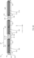
- Figs. 2A , 2B and 2C are schematic diagrams illustrating a flexible sheet 80 used to produce sensor 24, and Figs. 3 , 4A, 4B are schematic diagrams illustrating how the sheet is rolled up to form the sensor, according to an embodiment of the present invention.
- Fig. 2A illustrates a top portion of sheet 80, which is not explicitly claimed
- Fig. 2B illustrates a bottom portion of the sheet according to the claimed invention, both figures being viewed from above the sheet.
- Fig. 2C is a side view of sheet 80 according to the claimed invention.
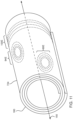
- Fig. 3 is a schematic perspective view of the formed sensor
- Fig. 4A is a schematic cross-section of the sensor as viewed along an axis of the sensor
- Fig. 4B is a schematic cross-section of a portion of the sensor as viewed orthogonal to the sensor axis.
- sheet 80 comprises a flexible insulating, substantially two-dimensional (2D), substrate 82, having a first side 84 and a second side 86.
- substrate 82 is formed from a polyimide material, but other embodiments may comprise any convenient flexible insulating material.
- sheet 80 is typically initially clad with conducting material, typically copper, on first side 84, while second side 86 does not have any conducting cladding.
- conducting side 84 is also referred to as conducting side 84
- side 86 is also referred to as non-conducting side 86.
- sheet 80 For clarity in the description of sheet 80, the sheet is assumed to be referenced to a set of xyz orthogonal axes, wherein the sheet lies in an xy plane, and there is a z axis normal to the sheet. In Figs. 2A and 2B the z axis is assumed to be directed out of the plane of the paper.
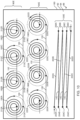
- a first set 90 which is not explicitly claimed, of conducting elements comprises a first plurality of spiral conductors 92.
- Fig. 2A illustrates four spiral conductors, identified as spiral conductors 92A, 92B, 92C, 92D.
- a second set 94 comprises a second plurality of spiral conductors 96, illustrated by way of example as spiral conductors 96A, 96B, 96C, 96D.
- a third set 100, illustrated in Fig. 2B comprises a third set of conductive lines 102, and in Fig. 2B there are by way example four lines 102A, 102B, 102C, and 102D.
- the spirals of first set 90 are positioned along a line segment parallel to the x-axis, and except as described below the spirals are generally similar.
- Each spiral of set 90 has an initial termination 110 and a final termination 112, so that the four example spirals in the figure have initial terminations 110A, 110B, 110C, 110D and final terminations 112A, 112B, 112C, 112D.
- Adjacent spirals are typically mirror images, in a yz mirror plane centered between the spirals, so that the spirals alternate between rotating in a right handed direction around a normal to sheet 80 and in a left handed direction about the normal.
- spiral conductors 92A, 92C rotate in a right handed direction
- spiral conductors 92B, 92D rotate in a left handed direction.
- spirals of set 90 are positioned along a line segment parallel to the x-axis. Furthermore, the spirals are separated from each other along the line segment, and the separations are such that when sheet 80 is rolled about itself, around an axis 150 parallel to the y-axis that is herein also termed the sensor axis, the spirals of set 90 align with themselves, as is illustrated schematically in Fig. 3 .
- initial terminations 110A, 110B, 110C, 110D align with themselves
- final terminations 112A, 112B, 112C, 112D also align with themselves.
- the separation of adjacent spirals on conducting side 84 is approximately constant, but differs because as sheet 80 rolls about itself, the distance of the sheet from the sheet axis increases.
- the sheet may be rolled about a former 83 as illustrated in Fig. 3 .
- the sheet is rolled about itself, so there is no former present in sensor 24.
- former 83 is not shown.
- sensor 24 is approximately cylindrical, having a diameter of approximately 2 - 5 mm and a length of approximately 5 - 10 mm.
- sheet 80 is in a configuration termed a Swiss roll configuration.
- a first conductive via 130 penetrates through the first side of sheet 80 to the second side of the sheet to interconnect the initial termination of the given spiral with the initial termination of a spiral immediately above the given spiral.
- a second conductive via 132 penetrates through the first side of sheet 80 to the second side of the sheet to interconnect the final termination of the given spiral with the final termination of a spiral immediately below the given spiral.
- vias 130, 132 are shown as broken lines.
- Fig. 4A is a schematic cross-section of sensor 24, taken in a plane orthogonal to sensor axis 150
- Fig. 4B is a schematic cross-section of set 90 of the sensor, taken in a plane parallel to axis 150.
- Figs 4A and 4B illustrate the positioning of vias 130 and 132 as they interconnect spirals 92A, 92B, 92C, and 92D.
- spirals 92A and 92D are the end spirals of set 90.
- a first via 130 connects initial terminations 110B and 110C of spirals 92B, 92C
- a second via 132 connects final terminations 112C and 112D
- a second via 132 connects final terminations 112A and 112B.
- the end spirals are only connected to one other spiral by one termination of the end spiral and a via, and the other termination of the end spiral is not connected to any spiral.
- each spiral of set 94 has an initial termination 120 and a final termination 122, so that the four example spirals in the figure have initial terminations 120A, 120B, 120C, 120D and final terminations 122A, 122B, 122C, 122D.
- adjacent spirals are typically mirror images, in a yz mirror plane centered between the spirals, so that the spirals alternate between rotating in a right handed direction around a normal to sheet 80 and in a left handed direction about the normal.
- the spirals of set 94 are also positioned along a line segment parallel to the x-axis, and the spirals have substantially the same separations on the line segment as the spirals of set 90.
- the spirals of set 94 are also connected, by vias 130 and 132, substantially as described above for set 90.
- the line segment for set 94 is displaced relative to the line segment of set 90.
- the displacement is in both the x and the y directions.
- a y displacement 160 causes set 94 to be displaced, with respect to set 90, parallel to the sheet axis.
- y displacement 160 is illustrated in Figs. 2A and 2C , and in Fig. 3 .
- An x displacement 162 is selected so that in sensor 24, an angle ⁇ subtended by sets 90 and 94 to axis 150 is 90°.
- x displacement 162 is illustrated in Fig. 2A
- the corresponding angle ⁇ is illustrated in Fig. 4A .
- third set 100 of conducting elements comprises a plurality of conducting lines 102, and except for their terminations, the lines are typically parallel to the x axis and typically have equal lengths.
- the lines are displaced along the y axis relative to each other.
- Each line has an initial termination and a final termination, both of which are offset in the y direction from their respective line.
- the four example lines 102A, 102B, 102C, and 102D in the figure have initial terminations 104A, 104B, 104C, 104D and final terminations 106A, 106B, 106C, 106D respectively.
- Each conducting line 102 defines a ray on first side 84 of the substrate extending from its initial termination to its final termination, and the lines are laid out on surface 84 so that the rays of each line have a common direction.
- Fig. 2B illustrates two rays having the common direction, a first ray 108A from initial termination 104A to final termination 106A for line 102A, and a second ray 108D from initial termination 104D to final termination 106D for line 102D.
- the conducting lines of set 100 are displaced relative to each other, parallel to the y axis, so that in the rolled up configuration described above the initial termination of a given line 102 aligns with the final termination of a neighboring line 102. This alignment applies except for the initial termination of a "first" line of set 100 and for the final termination of a "last" line of the set, which are not aligned with any terminations.
- each pair of aligned terminations in set 100 is connected by a respective conductive via 140 which penetrates through the first side of sheet 80 to the second side of the sheet to interconnect the initial termination of a given line with the final termination of a neighboring line.
- Vias 140 are illustrated in Fig. 2B as broken lines.
- each set 90, 94, and 100 forms a respective coil, and each of the coils has two "free" terminations, i.e., terminations that are not connected to any other termination of the set.
- the coil of set 90 has free terminations 110A and 110D
- the coil of set 94 has free terminations 120A and 120D
- the coil of set 100 has free terminations 104A and 106D.
- each coil of sensor 24 thus operates, in response to an alternating magnetic field traversing the coil, in the same way as a coil of wire in the field, generating an alternating potential between the two free terminations of the coil.
- via connected sets 90. 94, and 100 behave as respective coils of wire, so that in the via connected state the sets are also referred to herein as coils.
- Fig. 5A is a schematic alternative depiction of sensor 24.
- the depiction shows an end view of the sensor viewed along sensor axis 150, and a side view of the sensor viewed orthogonal to the sensor axis.
- end view rolled up sheet 80 is shown as a circle, and sets 90, 94 are shown as arcs on the circle.
- side view sheet 80 is shown as a rectangle, sets 94 and 100 are lines on or in the rectangle, and set 90 is also shown as a rectangle.
- Fig. 5B is a schematic depiction of an exemplary sensor 224.
- the depiction of sensor 224 is similar to that of sensor 24 in Fig. 5A .
- the operation of sensor 224 is generally similar to that of sensor 24 ( Figs. 1 - 5A ), and elements indicated by the same reference numerals in both sensors 24 and 224 are generally similar in construction and in operation.
- a set of conducting elements 100A is generally similar in construction to set 100, as described above with respect to Fig. 2B and Fig. 3 .
- sets 94A and 90A correspond respectively in operation to sets 94 and 90 of sensor 24, the construction of sets 94A and 90A is different from that of sets 94 and 90.
- sets 94A and 90A lie in a common plane that is orthogonal to sensor axis 150, whereas sets 94 and 90 lie in different disjoint planes orthogonal to the sensor axis.
- the two sets of spirals lie on a common straight line segment.
- the different spirals of the two sets are interleaved, and are located on the line segment so that when sheet 80 is rolled up, the spirals of set 94A overlap and alternate in rotation direction.
- the spirals of set 90A overlap and alternate in rotation direction. Both sets of spirals are connected by vias as described above with respect to Fig. 2A .
- Fig. 5C is a schematic depiction of an exemplary sensor 324.
- the depiction of sensor 324 is similar to that of sensor 24 in Fig. 5A .
- the operation of sensor 324 is generally similar to that of sensor 224 ( Figs. 1 - 5A , 5B ), and elements indicated by the same reference numerals in both sensors 224 and 324 are generally similar in construction and in operation.
- sensor 324 comprises three pairs of similar coils, the coils in a given pair having a common axis of symmetry and being separated along the axis.
- the three axes of the three pairs are orthogonal to each other.
- each of a pair of conducting coils 100B1, 100B2 is generally similar to set 100A ( Fig. 5B ), the pair having a common axis of symmetry coincident with sensor axis 150, each of the coils in the pair defining a respective plane orthogonal to the axis, the planes being separated along the axis.
- each of a pair of conducting coils 94B1, 94B2 is generally similar to set 94A, the pair having a common axis of symmetry orthogonal to, and intersecting, sensor axis 150, and being separated along the axis.
- each of a pair of conducting coils 90B1, 90B2 is generally similar to set 90A ( Fig. 5B ), the pair having a common axis of symmetry orthogonal to sensor axis 150 and to the axis of coils 94B1, 94B2, and being separated along the axis.
- each pair in sensor 324 may be configured to act as a Helmholtz pair of coils, so that at the intersection of the three axes of symmetry there is a region of nearly uniform magnetic field.
- Fig. 5D is a schematic depiction of a plurality of exemplary sensors 424.
- the depiction of sensors 424 is similar to that of sensor 24 in Fig. 5A .
- the operation of sensors 424 is generally similar to that of sensor 24 ( Figs. 1 - 5A ), and elements indicated by the same reference numerals in both sensors 24 and 424 are generally similar in construction and in operation.
- sensors 424 In contrast to sensor 24, which comprises one set of orthogonal coils, sensors 424 comprise two or more sets of orthogonal coils. Each set is substantially similar to sensor 24. However, sensors 424 are constructed on a single sheet 80A, which has substantially the same properties as sheet 80 (described above). However, a length of sheet 80A, measured along a line parallel to the y axis, which is parallel, as explained above, to sensor axis 150, is typically larger than that of sheet 80, and the length is selected so as to accommodate the plurality of orthogonal sensors on sheet 80A.
- Figs. 6A , 6B , and 6C are schematic diagrams illustrating a flexible sheet 80C used to produce an exemplary sensor 524
- Fig. 7 is a schematic diagram illustrating how the sheet is rolled up to form the sensor.
- Fig. 6A illustrates a top portion of sheet 80C, which is not explicitly claimed
- Fig. 6B illustrates a bottom portion of the sheet according to the claimed invention, both figures being viewed from above the sheet.
- Fig. 6C is a side view of sheet 80C according to the claimed invention.
- Fig. 7 is a schematic perspective view of the formed sensor.
- sensor 524 is generally similar to that of sensor 24 ( Figs. 1 - 5A ), and elements indicated by the same reference numerals in both sensors 24 and 524 are generally similar in construction and in operation.
- sensor 524 comprises three coils oriented orthogonally to each other.
- Sensor 24 is formed from single sheet 80, which has single layers of conducting elements on conducting side 84 of the sheet for each of its coils, and there are no conducting elements within substrate 82 of the sheet.
- Sensor 524 is also formed from a single sheet 80C, which also has single layers of conducting elements on conducting side 84 of the sheet.
- sheet 80C there are one or more conducting elements, similar to and aligned with those on the conducting side, embedded in respective layers within substrate 82 of the sheet. As is described below, the multiple sets of aligned conducting elements are connected in parallel by vias.
- sheet 80C of sensor 524 there are two layers of conducting elements embedded in substrate 82, but embodiments of the present invention comprise any number of layers of conducting elements embedded in the substrate.
- a set 90C which is not explicitly claimed, of conducting elements comprises a plurality of spiral conductors 92, the same plurality of spiral conductors A92, and the same plurality of spiral conductors B92 ( Fig. 6C ).
- Spiral conductors 92 have been described above with reference to Fig. 2A .
- Spiral conductors A92 and B92 are congruent to spiral conductors 92, but are displaced from conductors 92 in the z direction.
- the initial terminations of the three sets of spiral conductors are connected by conducting vias 526, and the final terminations of the three sets are also connected by conducting vias 526. It will be understood that in set 90C there are four groups of spirals, each group comprising three spirals connected, by vias 526, in parallel.
- a set 94C of conducting elements comprises a plurality of spiral conductors 96, the same plurality of spiral conductors A96, and the same plurality of spiral conductors B96.
- Spiral conductors 96 have been described above with reference to Fig. 2A .
- Spiral conductors A96 and B96 are congruent to spiral conductors 96, but are displaced from conductors 96 in the z direction.
- the initial terminations of the three sets of spiral conductors are connected by conducting vias 526, and the final terminations of the three sets are also connected by conducting vias 526.
- set 90C in set 94C there are four groups of spirals, each group comprising three spirals connected, by vias 526, in parallel.
- a set 100C of conducting elements comprises a plurality of conductive lines 102, the same plurality of lines A102, and the same plurality of lines B102.
- Lines 102 have been described above with reference to Fig. 2B .
- Lines A102 and B102 are congruent to lines 102, but are displaced from lines 102 in the z direction.
- the initial terminations of the three sets of conductive lines are connected by conducting vias 526, and the final terminations of the three sets are also connected by conducting vias 526.
- Figs. 8A , 8B , and 8C are schematic diagrams illustrating flexible sheets 80, 80D, and 80E used to produce an exemplary sensor 624
- Fig. 9 is a schematic diagram illustrating how the sheets are rolled up to form the sensor.
- Fig. 8A illustrates a top portion of upper sheet 80, which is not explicitly claimed
- Fig. 8B illustrates a bottom portion of the upper sheet according to the claimed invention, both figures being viewed from above the sheet.
- Fig. 8C is a side view of the three sheets 80, 80D, and 80E according to the claimed invention.
- Fig. 9 is a schematic perspective view of the formed sensor.
- sensor 624 is generally similar to that of sensor 24 ( Figs. 1 - 5A ), and elements indicated by the same reference numerals in both sensors 24 and 624 are generally similar in construction and in operation.
- sensor 24 comprises three coils oriented orthogonally to each other.
- sensor 624 is formed from a plurality of substantially similar single sheets.
- sensor 624 is assumed to be formed from three sheets 80, 80D, and 80E.
- embodiments of the present invention may form sensors from any number of substantially identical sheets.
- Sheets 80D and 80E are substantially identical to each other and to sheet 80, described above with reference to sensor 24.
- sheets 80D and 80E have respective conducting sides 84D, 84E and non-conducting sides 86D, 86E ( Fig. 8C ).
- conducting side 84D there are a plurality of spiral conductors D92 and D96, and a set of conductive lines D102, which are respectively congruent to spiral conductors 92, 96 and lines 102.
- conducting side 84E there are a plurality of spiral conductors E92 and E96, and a set of conductive lines E102, which are respectively congruent to spiral conductors 92, 96 and lines 102.
- sheets 80, 80D, and 80E are stacked on each other so that the conducting side of one sheet contacts the non-conducting side of an abutting sheet, and so that congruent elements in each sheet align.
- sheet 80 overlays sheet 80D, which in turn overlays sheet 80E.
- set 90D comprises four groups of spirals, each group comprising three spirals connected in parallel by vias 526.
- Set 94D comprises four groups of spirals, each group comprising three spirals connected in parallel by vias 526.
- Set 102D comprises four groups of conductive line elements, each group comprising three conductive line elements connected in parallel by vias 526.
- Sensor 24 is formed on single sheet 80, which has single layers of conducting elements on conducting side 84 of the sheet for each of its coils, and there are no conducting elements within substrate 82 of the sheet.
- Sensor 524 is formed on a single sheet 80C, which also has single layers of conducting elements on conducting side 84 of the sheet.
- sheet 80C there are one or more conducting elements, similar to and aligned with those on the conducting side, embedded in respective layers within substrate 82 of the sheet. As is described below, the multiple sets of aligned conducting elements are connected in parallel by vias.
- Fig. 10 is a schematic diagram illustrating a flexible sheet 180, which is not explicitly claimed, used to produce an exemplary sensor 724
- Fig. 11 is a schematic diagram illustrating how the sheet is rolled up to form the sensor.
- the operation of sensor 724 is generally similar to that of sensor 24 ( Figs. 1 - 5A ), and elements indicated by the same reference numerals in both sensors 24 and 724 are generally similar in construction and in operation.
- each conducting line of the third coil of sensor 724 is a line, typically a straight line, from its initial to its final termination.
- Set 90E which is not explicitly claimed, comprises four curvilinear spirals 192A, 192B, 192C, and 192D which have respective initial terminations 210A, 210B, 210C, 210D and final terminations 212A, 212B, 212C, 212D, and as for set 90 of sensor 24, the spirals of set 90E are positioned on a straight line segment and adjacent spirals are mirror images of each other.
- spiral conductors 192A, 192C rotate in a right handed direction
- spiral conductors 192B, 192D rotate in a left handed direction.
- the spirals of set 90E align with themselves, so that initial terminations 210A, 210B, 210C, 210D align with themselves, and final terminations 212A, 212B, 212C, 212D also align with themselves.
- an initial termination is connected by a via to an initial termination of an adjacent spiral
- a final termination is connected by a via to a final termination.
- vias 130 connect initial terminations 210A and 210B, 210C and 210D
- a via 132 connects final terminations 212B and 212C.
- End spirals 192A, 192D each have a respective final termination not connected to another spiral.
- spirals of set 94E are generally similar in layout and configuration to the spirals of set 90E.
- the four example spirals in the figure have initial terminations 220A, 220B, 220C, 220D and final terminations 222A, 222B, 222C, 222D.
- adjacent spirals are typically mirror images, in a mirror plane centered between the spirals, so that the spirals alternate between rotating in a right handed direction around a normal to sheet 180 and in a left handed direction about the normal.
- the spirals of set 94E are also positioned along a straight line segment parallel to the 90E line segment, and the spirals have substantially the same separations on their line segment as the spirals of set 90E.
- the spirals of set 94E align with themselves, as do the initial and final terminations of the set.
- the terminations are also connected, by vias 130 and 132, as is illustrated in Fig. 10 .
- the line segment for set 94E is displaced relative to the line segment of set 90E.
- the displacement is substantially as described above for sensor 24 and is such that in the rolled up configuration of sensor 724 an angle subtended by sets 90E and 94E to sensor axis 150 is 90°.
- third set 100E of conducting lines of sensor 724 do not have initial terminations and final terminations which are offset from the lines; rather each conducting line of the third set, that forms a third coil of sensor 724, is a line, herein assumed to be a straight line, from its initial to its final termination.
- conducting lines 202A, 202B, 202C, and 202D are lines between respective initial terminations 204A, 204B, 204C, and 204D and respective final terminations 206A, 206B, 206C, and 206D.
- the conducting lines of set 100E are displaced relative to each other, parallel to sensor axis 150, so that in the rolled up configuration of the sensor the initial termination of a given line in set 100E aligns with the final termination of a neighboring line on the set.
- This alignment applies except for the initial termination of a "first" line of set 100E and for the final termination of a "last" line of the set, which are not aligned with any terminations.
- the aligned terminations are connected by vias.
- initial termination 204B aligns with, and is connected by a via 140 to, final termination 206A
- initial termination 204C aligns with, and is connected by a via 140 to, final termination 206B
- initial termination 204D aligns with, and is connected by a via 140 to, final termination 206C.
- vias 140 penetrate through the first side of sheet 180 to the second side of the sheet to interconnect the initial termination of a given line with the final termination of a neighboring line.
- each of sets 90E, 94E, and 100E have two "free" terminations. If current is input to one of the free terminations of a coil it exits from the other free termination, as is illustrated by the arrows at terminations 212A and 212D, 222A and 222D, and 204A and 206D, and the current traverses all the elements of a given set in a common direction. Thus, as for sensor 24, the via connected sets of sensor 724 behave as respective coils of wire.
- inventions described above comprise rectilinear and curvilinear conducting lines, which are connected by vias to form coils.
- embodiments of the present invention are not limited to one type of conducting line, but may comprise mixtures of such lines.
- rectilinear conducting lines do not necessarily comprise sections which are orthogonal to each other, but rather may comprise sections making any convenient angles with each other, such as being sections of a hexagon or an octagon.
- conducting lines comprising sets such as set 100, it will be understood that at least a part of such lines may be curvilinear.
Landscapes
- Engineering & Computer Science (AREA)
- Health & Medical Sciences (AREA)
- Life Sciences & Earth Sciences (AREA)
- Physics & Mathematics (AREA)
- Microelectronics & Electronic Packaging (AREA)
- Surgery (AREA)
- Power Engineering (AREA)
- Public Health (AREA)
- Pathology (AREA)
- Biomedical Technology (AREA)
- Heart & Thoracic Surgery (AREA)
- Medical Informatics (AREA)
- Molecular Biology (AREA)
- Animal Behavior & Ethology (AREA)
- General Health & Medical Sciences (AREA)
- Biophysics (AREA)
- Veterinary Medicine (AREA)
- Manufacturing & Machinery (AREA)
- General Physics & Mathematics (AREA)
- Condensed Matter Physics & Semiconductors (AREA)
- Human Computer Interaction (AREA)
- Radiology & Medical Imaging (AREA)
- Nuclear Medicine, Radiotherapy & Molecular Imaging (AREA)
- Optics & Photonics (AREA)
- Cardiology (AREA)
- Coils Or Transformers For Communication (AREA)
- Structure Of Printed Boards (AREA)
- Transmission And Conversion Of Sensor Element Output (AREA)
- Production Of Multi-Layered Print Wiring Board (AREA)
- Printing Elements For Providing Electric Connections Between Printed Circuits (AREA)
- Geophysics And Detection Of Objects (AREA)
- Parts Printed On Printed Circuit Boards (AREA)
- Measurement Of Length, Angles, Or The Like Using Electric Or Magnetic Means (AREA)
- Measuring Magnetic Variables (AREA)
Claims (14)
- Substrat isolant flexible (82), ayant un premier côté (84) et un second côté (86), et pouvant être enroulé autour d'un axe de capteur (150) parallèle à un axe y du substrat ;une première ligne conductrice (102A) et une deuxième ligne conductrice (102B) formées sur le premier côté du substrat, la première ligne conductrice ayant une première terminaison initiale (104A) et une première terminaison finale (106A), dans lequel la première terminaison initiale (104A) et la première terminaison finale (106A) sont décalées par rapport à la première ligne conductrice (102A), respectivement sur des côtés opposés de la première ligne conductrice (102A), la deuxième ligne conductrice (102B) ayant une deuxième terminaison initiale (104B) et une deuxième terminaison finale (106B), dans lequel la deuxième terminaison initiale (104B) et la deuxième terminaison finale (106B) sont décalées par rapport à la deuxième ligne conductrice (102B), respectivement sur des côtés opposés de la deuxième ligne conductrice (102B), la première ligne définissant un premier rayon (108A) le long du substrat depuis la première terminaison initiale jusqu'à la première terminaison finale, la deuxième ligne définissant un deuxième rayon le long du substrat depuis la deuxième terminaison initiale jusqu'à la deuxième terminaison finale, les premier et deuxième rayons ayant une même direction, les lignes, à l'exception de leurs terminaisons, étant parallèles à l'axe x, ayant des longueurs égales et ayant un déplacement entre elles parallèle à l'axe y, avec une ampleur prédéfinie de sorte que lorsque le substrat est enroulé autour de l'axe du capteur, la première terminaison finale s'aligne sur la deuxième terminaison initiale ; etun trou d'interconnexion (140) pénétrant dans le substrat du premier côté au deuxième côté de manière à interconnecter la première terminaison finale et la deuxième terminaison initiale.
- Substrat isolant flexible selon la revendication 1, dans lequel au moins l'une des première et deuxième lignes conductrices (102) comprend un élément rectiligne.
- Substrat isolant flexible selon la revendication 1, dans lequel au moins l'une des première et deuxième lignes conductrices (102) comprend un élément curviligne.
- Substrat isolant flexible selon la revendication 1, et comprenant :une troisième ligne conductrice (102C) et une quatrième ligne conductrice (102D) formées sur le premier côté (84) du substrat (82), la troisième ligne conductrice ayant une troisième terminaison initiale (104C) et une troisième terminaison finale (106C), la quatrième ligne conductrice ayant une quatrième terminaison initiale (104D) et une quatrième terminaison finale (106D), la troisième ligne définissant un troisième rayon le long du substrat depuis la troisième terminaison initiale jusqu'à la troisième terminaison finale, la quatrième ligne définissant un quatrième rayon (108D) le long du substrat depuis la quatrième ligne de terminaison initiale jusqu'à la quatrième terminaison finale, les troisième et quatrième rayons ayant la même direction, les lignes, à l'exception de leurs terminaisons, étant parallèles à l'axe x, ayant des longueurs égales et ayant le déplacement, parallèle à l'axe y (150), avec l'ampleur prédéfinie entre elles, de sorte que, lorsque le substrat est enroulé autour de l'axe du capteur (150), la troisième terminaison finale s'aligne sur la quatrième terminaison initiale, et de sorte que les première et deuxième lignes définissent un premier plan orthogonal à l'axe du capteur, et que les troisième et quatrième lignes définissent un second plan, distinct du premier plan, orthogonal à l'axe du capteur ; etun deuxième trou d'interconnexion (140) pénétrant dans le substrat du premier côté (84) au deuxième côté (86) de manière à interconnecter la troisième terminaison finale et la quatrième terminaison initiale.
- Substrat isolant flexible selon la revendication 1, et comprenant :une ou plusieurs troisièmes lignes conductrices (102A, 102B) ayant des troisièmes terminaisons initiales et des troisièmes terminaisons finales respectives, la ou les troisièmes lignes conductrices étant intégrées dans le substrat (82) et définissant respectivement un ou plusieurs troisièmes rayons depuis les troisièmes terminaisons initiales respectives jusqu'aux terminaisons finales respectives, le ou les troisièmes rayons ayant la même direction, de sorte que les troisièmes terminaisons initiales respectives s'alignent sur la première terminaison initiale et que les troisièmes terminaisons finales respectives s'alignent sur la première terminaison finale ;un ou plusieurs seconds trous d'interconnexion (526) interconnectant les troisièmes terminaisons initiales respectives et la première terminaison initiale ; etun ou plusieurs troisièmes trous d'interconnexion (526) interconnectant les troisièmes terminaisons finales respectives et la première terminaison finale.
- Substrat isolant flexible selon la revendication 1, dans lequel le substrat isolant flexible (82) comprend une première feuille (80E), l'appareil comprenant en outre :une seconde feuille (80D), ayant un troisième côté (84D) et un quatrième côté (86D) qui vient en butée contre et recouvre le premier côté (84E) du premier substrat isolant flexible, enroulé autour de l'axe du capteur ;une troisième ligne conductrice (D102) formée sur le troisième côté de la seconde feuille, la troisième ligne conductrice ayant une troisième terminaison initiale et une troisième terminaison finale qui s'alignent respectivement sur la première terminaison initiale et la première terminaison finale ;un deuxième trou d'interconnexion (526) pénétrant dans la seconde feuille du troisième côté au quatrième côté de manière à interconnecter la troisième terminaison initiale et la première terminaison initiale ; etun troisième trou d'interconnexion (526) pénétrant dans le second substrat du troisième côté au quatrième côté de manière à interconnecter la troisième terminaison finale et la première terminaison finale de la première ligne.
- Capteur comprenant le substrat isolant flexible selon l'une quelconque revendication précédente, dans lequel le substrat isolant flexible a été enroulé pour former le capteur.
- Procédé de fabrication d'un substrat enroulé flexible, comprenant :la fourniture d'un substrat isolant flexible (82), ayant un premier côté (84) et un deuxième côté (86) ;la formation sur le premier côté du substrat d'une première ligne conductrice (102A) et d'une deuxième ligne conductrice (102B), la première ligne conductrice ayant une première terminaison initiale (104A) et une première terminaison finale (106A), dans lequel la première terminaison initiale (104A) et la première terminaison finale (106A) sont décalées par rapport à la première ligne conductrice (102A) respectivement sur des côtés opposés de la première ligne conductrice, la deuxième ligne conductrice ayant une deuxième terminaison initiale (104B) et une deuxième terminaison finale (106B), dans lequel la deuxième terminaison initiale (104B) et la deuxième terminaison finale (106B) sont décalées par rapport à la deuxième ligne conductrice (102B) respectivement sur des côtés opposés de la deuxième ligne conductrice, la première ligne définissant un premier rayon (108A) le long du substrat depuis la première terminaison initiale jusqu'à la première terminaison finale, la deuxième ligne définissant un deuxième rayon le long du substrat depuis la deuxième terminaison initiale jusqu'à la deuxième terminaison finale, les premier et deuxième rayons ayant une même direction, les lignes, à l'exception de leurs terminaisons, étant parallèles à l'axe x, ayant des longueurs égales et ayant entre elles un déplacement parallèle à l'axe y, avec une amplitude prédéfinie, de sorte que lorsque le substrat est enroulé autour d'un axe de capteur (150) parallèle à l'axe y, la première terminaison finale s'aligne sur la deuxième terminaison initiale ; etla pénétration du substrat avec un trou d'interconnexion (140) du premier côté au deuxième côté de manière à interconnecter la première terminaison finale et la deuxième terminaison initiale ; etle roulement du substrat souple autour de l'axe du capteur parallèle au substrat ;
- Procédé selon la revendication 8, dans lequel au moins l'une des première et deuxième lignes conductrices (102) comprend un élément rectiligne.
- Procédé selon la revendication 8, dans lequel au moins l'une des première et deuxième lignes conductrices (102) comprend un élément curviligne.
- Procédé selon la revendication 8, et comprenant :la formation sur le premier côté (84) du substrat (82) d'une troisième ligne conductrice (102C) et d'une quatrième ligne conductrice (102D), la troisième ligne conductrice ayant une troisième terminaison initiale (104C) et une troisième terminaison finale (106C), la quatrième ligne conductrice ayant une quatrième terminaison initiale (104D) et une quatrième terminaison finale (106D), la troisième ligne définissant un troisième rayon le long du substrat depuis la troisième terminaison initiale jusqu'à la troisième terminaison finale, la quatrième ligne définissant un quatrième rayon (108D) le long du substrat depuis la quatrième ligne de terminaison initiale jusqu'à la quatrième terminaison finale, les troisième et quatrième rayons ayant la même direction, les lignes, à l'exception de leurs terminaisons, étant parallèles à l'axe x, ayant des longueurs égales et ayant le déplacement, parallèle à l'axe y (150), avec l'ampleur prédéfinie entre elles, de sorte que, lorsque le substrat est enroulé autour de l'axe du capteur, la troisième terminaison finale s'aligne sur la quatrième terminaison initiale, et que les première et deuxième lignes définissent un premier plan orthogonal à l'axe du capteur, et que les troisième et quatrième lignes définissent un second plan, distinct du premier plan, orthogonal à l'axe du capteur ; etla pénétration du substrat avec un deuxième trou d'interconnexion (140) du premier côté au deuxième côté de manière à interconnecter la troisième terminaison finale et la quatrième terminaison initiale.
- Procédé selon la revendication 8, et comprenant :l'intégration dans le substrat (82) d'une ou plusieurs troisièmes lignes conductrices (102A, 102B) ayant des troisièmes terminaisons initiales et des troisièmes terminaisons finales respectives, la ou les troisièmes lignes conductrices définissant un ou plusieurs troisièmes rayons depuis les troisièmes terminaisons initiales respectives jusqu'aux terminaisons finales respectives, le ou les troisièmes rayons ayant la même direction, de sorte que les troisièmes terminaisons initiales respectives s'alignent sur la première terminaison initiale et que les troisièmes terminaisons finales respectives s'alignent sur la première terminaison finale ;l'interconnexion avec un ou plusieurs seconds trous d'interconnexion (526) des troisièmes terminaisons initiales respectives et de la première terminaison initiale ; etl'interconnexion avec un ou plusieurs troisièmes trous d'interconnexion (526) des troisièmes terminaisons finales respectives et de la première terminaison finale.
- Procédé selon la revendication 8, dans lequel le substrat isolant flexible (82) comprend une première feuille (80E), le procédé comprenant en outre :la fourniture d'une seconde feuille (80D), ayant un troisième côté (84D) et un quatrième côté (86D) venant en butée contre et recouvrant le premier côté (84E) de la première feuille, enroulée autour de l'axe du capteur (150) ;la formation d'une troisième ligne conductrice (D102) sur le troisième côté de la seconde feuille, la troisième ligne conductrice ayant une troisième terminaison initiale et une troisième terminaison finale qui s'alignent respectivement sur la première terminaison initiale et la première terminaison finale ;la pénétration de la seconde feuille avec un deuxième trou d'interconnexion (526) du troisième côté au quatrième côté de manière à interconnecter la troisième terminaison initiale et la première terminaison initiale ; etla pénétration de la seconde feuille avec un troisième trou d'interconnexion (526) du troisième côté au quatrième côté de manière à interconnecter la troisième terminaison finale et la première terminaison finale de la première ligne.
- Procédé selon l'une quelconque des revendications 8 à 13, dans lequel le procédé forme un capteur.
Applications Claiming Priority (2)
| Application Number | Priority Date | Filing Date | Title |
|---|---|---|---|
| US15/390,388 US10330742B2 (en) | 2016-12-23 | 2016-12-23 | Triple axis sensor on a single layer printed circuit |
| EP17210158.6A EP3340750B1 (fr) | 2016-12-23 | 2017-12-22 | Carte de circuit imprimé flexible pour capteur à trois axes |
Related Parent Applications (2)
| Application Number | Title | Priority Date | Filing Date |
|---|---|---|---|
| EP17210158.6A Division-Into EP3340750B1 (fr) | 2016-12-23 | 2017-12-22 | Carte de circuit imprimé flexible pour capteur à trois axes |
| EP17210158.6A Division EP3340750B1 (fr) | 2016-12-23 | 2017-12-22 | Carte de circuit imprimé flexible pour capteur à trois axes |
Publications (3)
| Publication Number | Publication Date |
|---|---|
| EP3340751A1 EP3340751A1 (fr) | 2018-06-27 |
| EP3340751C0 EP3340751C0 (fr) | 2025-01-29 |
| EP3340751B1 true EP3340751B1 (fr) | 2025-01-29 |
Family
ID=60888232
Family Applications (2)
| Application Number | Title | Priority Date | Filing Date |
|---|---|---|---|
| EP18150488.7A Active EP3340751B1 (fr) | 2016-12-23 | 2017-12-22 | Capteur à trois axes sur un circuit imprimé monocouche |
| EP17210158.6A Active EP3340750B1 (fr) | 2016-12-23 | 2017-12-22 | Carte de circuit imprimé flexible pour capteur à trois axes |
Family Applications After (1)
| Application Number | Title | Priority Date | Filing Date |
|---|---|---|---|
| EP17210158.6A Active EP3340750B1 (fr) | 2016-12-23 | 2017-12-22 | Carte de circuit imprimé flexible pour capteur à trois axes |
Country Status (7)
| Country | Link |
|---|---|
| US (1) | US10330742B2 (fr) |
| EP (2) | EP3340751B1 (fr) |
| JP (1) | JP6953301B2 (fr) |
| CN (1) | CN108241132B (fr) |
| AU (1) | AU2017268693A1 (fr) |
| CA (1) | CA2989346A1 (fr) |
| IL (1) | IL255857A0 (fr) |
Families Citing this family (15)
| Publication number | Priority date | Publication date | Assignee | Title |
|---|---|---|---|---|
| US10842438B2 (en) * | 2018-02-20 | 2020-11-24 | Arizona Board Of Regents On Behalf Of Arizona State University | Swallowable, food-based, digestible wireless device for measuring gastric pH |
| DE102019115405A1 (de) * | 2019-06-06 | 2020-12-10 | Balluff Gmbh | Spulenvorrichtung und Verfahren zur Herstellung einer Spulenvorrichtung |
| US20210177355A1 (en) * | 2019-12-11 | 2021-06-17 | Biosense Webster (Israel) Ltd. | Balloon Catheter with Position Sensors |
| US11712295B2 (en) * | 2019-12-30 | 2023-08-01 | Biosense Webster (Israel) Ltd. | Multi-purpose sensing and radiofrequency (RF) ablation spiral electrode for catheter |
| CN111785472B (zh) * | 2020-06-22 | 2022-07-01 | 上海卫星工程研究所 | 双超卫星磁浮低电阻pcb线圈 |
| US12082875B2 (en) * | 2020-09-24 | 2024-09-10 | Biosense Webster (Israel) Ltd | Balloon catheter having a coil for sensing tissue temperature and position of the balloon |
| US20220095947A1 (en) | 2020-09-29 | 2022-03-31 | Biosense Webster (Israel) Ltd. | Circular navigation catheter with surface mounted inductive navigation sensors |
| US20230181241A1 (en) * | 2021-12-10 | 2023-06-15 | Biosense Webster (Israel) Ltd. | Electrical paths along flexible section of deflectable sheath |
| IT202200000779A1 (it) * | 2022-01-19 | 2023-07-19 | Fondazione St Italiano Tecnologia | Sensore a circuito stampato flessibile |
| US20240216055A1 (en) | 2022-12-29 | 2024-07-04 | Biosense Webster (Israel) Ltd. | Fractal cylindrical cage systems and methods for distributed tissue contact for mapping and ablation |
| US20240216052A1 (en) | 2022-12-29 | 2024-07-04 | Biosense Webster (Israel) Ltd. | Systems and methods for cylindrical cage mapping and ablation catheters having flexible circuits |
| US20240216053A1 (en) | 2022-12-29 | 2024-07-04 | Biosense Webster (Israel) Ltd. | Systems and methods for cylindrical cage mapping and ablation catheters having integrated electrodes |
| US20240216054A1 (en) | 2022-12-29 | 2024-07-04 | Biosense Webster (Israel) Ltd. | Systems and methods for cylindrical cage mapping and ablation catheters comprising flexible circuits |
| US20240216075A1 (en) | 2022-12-30 | 2024-07-04 | Biosense Webster (Israel) Ltd. | Position and force sensors for catheters |
| US20240390056A1 (en) | 2023-05-23 | 2024-11-28 | Biosense Webster (Israel) Ltd. | End effector having elongated support member with curved electrode landing region |
Citations (1)
| Publication number | Priority date | Publication date | Assignee | Title |
|---|---|---|---|---|
| US20030187347A1 (en) * | 2001-02-15 | 2003-10-02 | Robin Medical Inc. | Endoscopic examining apparatus particularly useful in MRI, a probe useful in such apparatus, and a method of making such probe |
Family Cites Families (38)
| Publication number | Priority date | Publication date | Assignee | Title |
|---|---|---|---|---|
| JPH06109820A (ja) * | 1992-09-25 | 1994-04-22 | Hitachi Ltd | 3次元検出コイル |
| JPH09246035A (ja) * | 1996-03-06 | 1997-09-19 | Jeol Ltd | 回路印刷シート |
| JPH10289816A (ja) * | 1997-04-15 | 1998-10-27 | Omron Corp | プリント型積層コイル及びその製造方法 |
| US6097976A (en) | 1998-02-27 | 2000-08-01 | Ep Technologies, Inc. | Catheter distal end assemblies with bonded surface coatings |
| US20030029345A1 (en) * | 1998-03-11 | 2003-02-13 | Tiernan Timothy C. | Ultra sensitive magnetic field sensors |
| US6320382B1 (en) * | 1999-12-23 | 2001-11-20 | Varian, Inc. | Etched z-axis gradient coils for magnetic resonance |
| EP1311188A1 (fr) | 2000-08-24 | 2003-05-21 | Volcano Therapeutics, Inc. | Catheter de thermographie dote de detecteurs thermiques de circuit flexible |
| DE10130130B4 (de) | 2001-06-22 | 2007-09-20 | Minebea Co., Ltd. | Vorrichtung zur Erzeugung eines drehzahlabhängigen Signals für einen Elektromotor, insbesondere für einen elektronisch kommutierten Gleichstrommotor |
| JP2005052637A (ja) * | 2003-07-18 | 2005-03-03 | Pentax Corp | カプセル型装置及びカプセル型装置駆動制御システム |
| US7229437B2 (en) | 2003-09-22 | 2007-06-12 | St. Jude Medical, Atrial Fibrillation Division, Inc. | Medical device having integral traces and formed electrodes |
| US8147486B2 (en) | 2003-09-22 | 2012-04-03 | St. Jude Medical, Atrial Fibrillation Division, Inc. | Medical device with flexible printed circuit |
| US8046050B2 (en) * | 2004-03-05 | 2011-10-25 | Biosense Webster, Inc. | Position sensing system for orthopedic applications |
| JP4426430B2 (ja) | 2004-12-15 | 2010-03-03 | 日東電工株式会社 | カテーテル及びその製造方法 |
| JP4648063B2 (ja) | 2005-04-19 | 2011-03-09 | 日東電工株式会社 | カテーテル用フレキシブル配線回路基板、並びに、該フレキシブル配線回路基板を用いたカテーテル及びその製造方法 |
| US8730011B2 (en) * | 2005-07-14 | 2014-05-20 | Biosense Webster, Inc. | Wireless position transducer with digital signaling |
| US7301332B2 (en) * | 2005-10-06 | 2007-11-27 | Biosense Webster, Inc. | Magnetic sensor assembly |
| US8203343B1 (en) | 2005-10-12 | 2012-06-19 | Seektech, Inc. | Reconfigurable portable locator employing multiple sensor array having flexible nested orthogonal antennas |
| DE102007045874A1 (de) * | 2007-09-25 | 2009-04-02 | Ceos Corrected Electron Optical Systems Gmbh | Multipolspulen |
| US9037213B2 (en) * | 2008-01-08 | 2015-05-19 | Robin Medical Inc. | Method and apparatus to estimate location and orientation of objects during magnetic resonance imaging |
| US8628493B2 (en) * | 2008-06-03 | 2014-01-14 | The Feinstein Institute For Medical Research | Flexible spirally-rolled polymer tube for monitoring and treatment of brain injuries |
| JP2010278348A (ja) * | 2009-05-29 | 2010-12-09 | Alps Electric Co Ltd | 面実装型空芯コイル |
| US8543190B2 (en) | 2010-07-30 | 2013-09-24 | Medtronic, Inc. | Inductive coil device on flexible substrate |
| US8560086B2 (en) | 2010-12-02 | 2013-10-15 | St. Jude Medical, Atrial Fibrillation Division, Inc. | Catheter electrode assemblies and methods of construction therefor |
| CN102426344B (zh) * | 2011-08-30 | 2013-08-21 | 江苏多维科技有限公司 | 三轴磁场传感器 |
| US10258255B2 (en) * | 2011-09-14 | 2019-04-16 | St. Jude Medical International Holding S.àr.l. | Method for producing a miniature electromagnetic coil using flexible printed circuitry |
| KR101363020B1 (ko) * | 2011-10-31 | 2014-02-26 | 주식회사 세라젬메디시스 | 다중 반응 바이오센서 |
| EP2844333B1 (fr) * | 2012-04-23 | 2018-01-10 | Siemens Healthcare Diagnostics Inc. | Réseau de détecteurs |
| EP2948090B1 (fr) | 2013-01-23 | 2018-09-12 | Medtronic Xomed, Inc. | Instrument chirurgical à navigation comprenant une feuille de circuit souple |
| TWI513993B (zh) * | 2013-03-26 | 2015-12-21 | Ind Tech Res Inst | 三軸磁場感測器、製作磁場感測結構的方法與磁場感測電路 |
| US8941392B1 (en) * | 2013-08-17 | 2015-01-27 | Bend Labs, Inc. | Angular displacement sensor of compliant material |
| HUE039503T2 (hu) * | 2013-12-05 | 2019-01-28 | Nowtechnologies Zrt | Személyszállító eszköz, valamint ahhoz való vezérlõberendezés és vezérlõ eljárás |
| TWI574482B (zh) | 2014-04-16 | 2017-03-11 | 外崔色堤股份公司 | 用於行動裝置應用之無線能源轉換系統 |
| US9347764B2 (en) * | 2014-04-23 | 2016-05-24 | American Axle & Manufacturing, Inc. | Sensor assembly configured to sense target movement in first direction and insensitive to target movement in second and third directions orthogonal to first direction |
| US20170358841A1 (en) | 2014-10-21 | 2017-12-14 | Medella Health Inc. | Multi-layer micro receiver for a wireless communication system |
| US10603105B2 (en) | 2014-10-24 | 2020-03-31 | Boston Scientific Scimed Inc | Medical devices with a flexible electrode assembly coupled to an ablation tip |
| DK3349000T3 (da) | 2014-11-28 | 2020-02-17 | Parker Hannifin Mfg Limited | Sensorindretning |
| US11559349B2 (en) | 2016-09-12 | 2023-01-24 | Biosense Webster (Israel) Ltd. | Ablation catheter with a flexible printed circuit board |
| US10898262B2 (en) | 2016-10-25 | 2021-01-26 | Biosense Webster (Israel) Ltd. | Catheter distal end made of plastic tube and flexible printed circuit boards |
-
2016
- 2016-12-23 US US15/390,388 patent/US10330742B2/en active Active
-
2017
- 2017-11-22 IL IL255857A patent/IL255857A0/en active IP Right Grant
- 2017-12-04 AU AU2017268693A patent/AU2017268693A1/en not_active Abandoned
- 2017-12-15 CA CA2989346A patent/CA2989346A1/fr not_active Abandoned
- 2017-12-22 EP EP18150488.7A patent/EP3340751B1/fr active Active
- 2017-12-22 CN CN201711404009.9A patent/CN108241132B/zh active Active
- 2017-12-22 EP EP17210158.6A patent/EP3340750B1/fr active Active
- 2017-12-22 JP JP2017245978A patent/JP6953301B2/ja active Active
Patent Citations (1)
| Publication number | Priority date | Publication date | Assignee | Title |
|---|---|---|---|---|
| US20030187347A1 (en) * | 2001-02-15 | 2003-10-02 | Robin Medical Inc. | Endoscopic examining apparatus particularly useful in MRI, a probe useful in such apparatus, and a method of making such probe |
Also Published As
| Publication number | Publication date |
|---|---|
| JP2018113439A (ja) | 2018-07-19 |
| US10330742B2 (en) | 2019-06-25 |
| AU2017268693A1 (en) | 2018-07-12 |
| JP6953301B2 (ja) | 2021-10-27 |
| CN108241132A (zh) | 2018-07-03 |
| EP3340750C0 (fr) | 2024-08-07 |
| EP3340750B1 (fr) | 2024-08-07 |
| IL255857A0 (en) | 2017-12-31 |
| CN108241132B (zh) | 2021-12-07 |
| EP3340751C0 (fr) | 2025-01-29 |
| EP3340750A1 (fr) | 2018-06-27 |
| EP3340751A1 (fr) | 2018-06-27 |
| CA2989346A1 (fr) | 2018-06-23 |
| US20180180684A1 (en) | 2018-06-28 |
Similar Documents
| Publication | Publication Date | Title |
|---|---|---|
| EP3340751B1 (fr) | Capteur à trois axes sur un circuit imprimé monocouche | |
| US20250160716A1 (en) | Multi-axial position sensors printed on a folded flexible circuit board | |
| ES2293172T3 (es) | Deteccion de perturbaciones asociadas a metales en un sistema de rastreo magnetico. | |
| US7761100B2 (en) | Ultra-low frequency electromagnetic tracking system | |
| CN102188246B (zh) | 磁跟踪系统、设备及方法 | |
| US5711299A (en) | Surgical guidance method and system for approaching a target within a body | |
| EP2670300B1 (fr) | Agencement de bobine plane pour un appareil de mesure de l'impedance a induction magnetique | |
| US20140276004A1 (en) | Navigated Surgical Instrument | |
| JP5393953B2 (ja) | 医用トラッキング・システム向けの共形的コイルアレイ | |
| KR20030048374A (ko) | 전위 기록기 위치 지정 장치 및 방법 | |
| MXPA06011505A (es) | Ensamble de detector magnetico. | |
| CN109564244A (zh) | 检查辅助具、具备所述辅助具的基板检查装置及检查辅助具的制造方法 | |
| EP2770912A1 (fr) | Aiguille de biopsie détectable | |
| EP3973909A1 (fr) | Cathéter de navigation circulaire ayant des capteurs de navigation inductifs montés en surface | |
| JP7191943B2 (ja) | ケーブル及び関連する導通監視システム | |
| JP5546597B2 (ja) | 医療機器用ハーネス及び医療機器の組立方法 | |
| CN103519814B (zh) | 具有合成孔径mri传感器的导管 | |
| US7068359B2 (en) | Contactless system for measuring centricity and diameter | |
| JP7475934B2 (ja) | 三次元配線アセンブリを用いた磁気ピックアップの打ち消し | |
| JP2023540958A (ja) | 結合された位置確認エージェントを含むシステムおよび方法 | |
| KR101525992B1 (ko) | 3차원 스캐너 및 그 시스템 | |
| Weinschel et al. | Antenna Performance Verification at Launch Site. A Feasibility Study on Preflight Performance Testing of Stripline Slot Arrays Mounted on a Rocket. |
Legal Events
| Date | Code | Title | Description |
|---|---|---|---|
| PUAI | Public reference made under article 153(3) epc to a published international application that has entered the european phase |
Free format text: ORIGINAL CODE: 0009012 |
|
| STAA | Information on the status of an ep patent application or granted ep patent |
Free format text: STATUS: THE APPLICATION HAS BEEN PUBLISHED |
|
| AC | Divisional application: reference to earlier application |
Ref document number: 3340750 Country of ref document: EP Kind code of ref document: P |
|
| AK | Designated contracting states |
Kind code of ref document: A1 Designated state(s): AL AT BE BG CH CY CZ DE DK EE ES FI FR GB GR HR HU IE IS IT LI LT LU LV MC MK MT NL NO PL PT RO RS SE SI SK SM TR |
|
| AX | Request for extension of the european patent |
Extension state: BA ME |
|
| STAA | Information on the status of an ep patent application or granted ep patent |
Free format text: STATUS: REQUEST FOR EXAMINATION WAS MADE |
|
| 17P | Request for examination filed |
Effective date: 20181213 |
|
| RBV | Designated contracting states (corrected) |
Designated state(s): AL AT BE BG CH CY CZ DE DK EE ES FI FR GB GR HR HU IE IS IT LI LT LU LV MC MK MT NL NO PL PT RO RS SE SI SK SM TR |
|
| STAA | Information on the status of an ep patent application or granted ep patent |
Free format text: STATUS: EXAMINATION IS IN PROGRESS |
|
| 17Q | First examination report despatched |
Effective date: 20210625 |
|
| GRAP | Despatch of communication of intention to grant a patent |
Free format text: ORIGINAL CODE: EPIDOSNIGR1 |
|
| STAA | Information on the status of an ep patent application or granted ep patent |
Free format text: STATUS: GRANT OF PATENT IS INTENDED |
|
| INTG | Intention to grant announced |
Effective date: 20240416 |
|
| GRAJ | Information related to disapproval of communication of intention to grant by the applicant or resumption of examination proceedings by the epo deleted |
Free format text: ORIGINAL CODE: EPIDOSDIGR1 |
|
| STAA | Information on the status of an ep patent application or granted ep patent |
Free format text: STATUS: EXAMINATION IS IN PROGRESS |
|
| GRAP | Despatch of communication of intention to grant a patent |
Free format text: ORIGINAL CODE: EPIDOSNIGR1 |
|
| STAA | Information on the status of an ep patent application or granted ep patent |
Free format text: STATUS: GRANT OF PATENT IS INTENDED |
|
| INTC | Intention to grant announced (deleted) | ||
| INTG | Intention to grant announced |
Effective date: 20240903 |
|
| GRAS | Grant fee paid |
Free format text: ORIGINAL CODE: EPIDOSNIGR3 |
|
| GRAA | (expected) grant |
Free format text: ORIGINAL CODE: 0009210 |
|
| STAA | Information on the status of an ep patent application or granted ep patent |
Free format text: STATUS: THE PATENT HAS BEEN GRANTED |
|
| AC | Divisional application: reference to earlier application |
Ref document number: 3340750 Country of ref document: EP Kind code of ref document: P |
|
| AK | Designated contracting states |
Kind code of ref document: B1 Designated state(s): AL AT BE BG CH CY CZ DE DK EE ES FI FR GB GR HR HU IE IS IT LI LT LU LV MC MK MT NL NO PL PT RO RS SE SI SK SM TR |
|
| REG | Reference to a national code |
Ref country code: GB Ref legal event code: FG4D |
|
| REG | Reference to a national code |
Ref country code: CH Ref legal event code: EP |
|
| REG | Reference to a national code |
Ref country code: DE Ref legal event code: R096 Ref document number: 602017087609 Country of ref document: DE |
|
| REG | Reference to a national code |
Ref country code: IE Ref legal event code: FG4D |
|
| U01 | Request for unitary effect filed |
Effective date: 20250217 |
|
| U07 | Unitary effect registered |
Designated state(s): AT BE BG DE DK EE FI FR IT LT LU LV MT NL PT RO SE SI Effective date: 20250224 |
|
| PG25 | Lapsed in a contracting state [announced via postgrant information from national office to epo] |
Ref country code: RS Free format text: LAPSE BECAUSE OF FAILURE TO SUBMIT A TRANSLATION OF THE DESCRIPTION OR TO PAY THE FEE WITHIN THE PRESCRIBED TIME-LIMIT Effective date: 20250429 |
|
| PG25 | Lapsed in a contracting state [announced via postgrant information from national office to epo] |
Ref country code: PL Free format text: LAPSE BECAUSE OF FAILURE TO SUBMIT A TRANSLATION OF THE DESCRIPTION OR TO PAY THE FEE WITHIN THE PRESCRIBED TIME-LIMIT Effective date: 20250129 |
|
| PG25 | Lapsed in a contracting state [announced via postgrant information from national office to epo] |
Ref country code: ES Free format text: LAPSE BECAUSE OF FAILURE TO SUBMIT A TRANSLATION OF THE DESCRIPTION OR TO PAY THE FEE WITHIN THE PRESCRIBED TIME-LIMIT Effective date: 20250129 |
|
| PG25 | Lapsed in a contracting state [announced via postgrant information from national office to epo] |
Ref country code: NO Free format text: LAPSE BECAUSE OF FAILURE TO SUBMIT A TRANSLATION OF THE DESCRIPTION OR TO PAY THE FEE WITHIN THE PRESCRIBED TIME-LIMIT Effective date: 20250429 Ref country code: IS Free format text: LAPSE BECAUSE OF FAILURE TO SUBMIT A TRANSLATION OF THE DESCRIPTION OR TO PAY THE FEE WITHIN THE PRESCRIBED TIME-LIMIT Effective date: 20250529 |
|
| PG25 | Lapsed in a contracting state [announced via postgrant information from national office to epo] |
Ref country code: HR Free format text: LAPSE BECAUSE OF FAILURE TO SUBMIT A TRANSLATION OF THE DESCRIPTION OR TO PAY THE FEE WITHIN THE PRESCRIBED TIME-LIMIT Effective date: 20250129 |
|
| PG25 | Lapsed in a contracting state [announced via postgrant information from national office to epo] |
Ref country code: GR Free format text: LAPSE BECAUSE OF FAILURE TO SUBMIT A TRANSLATION OF THE DESCRIPTION OR TO PAY THE FEE WITHIN THE PRESCRIBED TIME-LIMIT Effective date: 20250430 |
|
| PG25 | Lapsed in a contracting state [announced via postgrant information from national office to epo] |
Ref country code: SM Free format text: LAPSE BECAUSE OF FAILURE TO SUBMIT A TRANSLATION OF THE DESCRIPTION OR TO PAY THE FEE WITHIN THE PRESCRIBED TIME-LIMIT Effective date: 20250129 |
|
| PG25 | Lapsed in a contracting state [announced via postgrant information from national office to epo] |
Ref country code: CZ Free format text: LAPSE BECAUSE OF FAILURE TO SUBMIT A TRANSLATION OF THE DESCRIPTION OR TO PAY THE FEE WITHIN THE PRESCRIBED TIME-LIMIT Effective date: 20250129 |
|
| PG25 | Lapsed in a contracting state [announced via postgrant information from national office to epo] |
Ref country code: SK Free format text: LAPSE BECAUSE OF FAILURE TO SUBMIT A TRANSLATION OF THE DESCRIPTION OR TO PAY THE FEE WITHIN THE PRESCRIBED TIME-LIMIT Effective date: 20250129 |