EP3335239B1 - Procédé de fabrication d'une structure semi-conductrice avec collage direct temporaire exploitant une couche poreuse - Google Patents
Procédé de fabrication d'une structure semi-conductrice avec collage direct temporaire exploitant une couche poreuse Download PDFInfo
- Publication number
- EP3335239B1 EP3335239B1 EP16750789.6A EP16750789A EP3335239B1 EP 3335239 B1 EP3335239 B1 EP 3335239B1 EP 16750789 A EP16750789 A EP 16750789A EP 3335239 B1 EP3335239 B1 EP 3335239B1
- Authority
- EP
- European Patent Office
- Prior art keywords
- substrate
- handle substrate
- handled
- disassembly
- bonding
- Prior art date
- Legal status (The legal status is an assumption and is not a legal conclusion. Google has not performed a legal analysis and makes no representation as to the accuracy of the status listed.)
- Active
Links
Images


Classifications
-
- H—ELECTRICITY
- H10—SEMICONDUCTOR DEVICES; ELECTRIC SOLID-STATE DEVICES NOT OTHERWISE PROVIDED FOR
- H10P—GENERIC PROCESSES OR APPARATUS FOR THE MANUFACTURE OR TREATMENT OF DEVICES COVERED BY CLASS H10
- H10P90/00—Preparation of wafers not covered by a single main group of this subclass, e.g. wafer reinforcement
- H10P90/19—Preparing inhomogeneous wafers
- H10P90/1904—Preparing vertically inhomogeneous wafers
- H10P90/1906—Preparing SOI wafers
- H10P90/1914—Preparing SOI wafers using bonding
-
- C—CHEMISTRY; METALLURGY
- C09—DYES; PAINTS; POLISHES; NATURAL RESINS; ADHESIVES; COMPOSITIONS NOT OTHERWISE PROVIDED FOR; APPLICATIONS OF MATERIALS NOT OTHERWISE PROVIDED FOR
- C09J—ADHESIVES; NON-MECHANICAL ASPECTS OF ADHESIVE PROCESSES IN GENERAL; ADHESIVE PROCESSES NOT PROVIDED FOR ELSEWHERE; USE OF MATERIALS AS ADHESIVES
- C09J5/00—Adhesive processes in general; Adhesive processes not provided for elsewhere, e.g. relating to primers
- C09J5/06—Adhesive processes in general; Adhesive processes not provided for elsewhere, e.g. relating to primers involving heating of the applied adhesive
-
- H—ELECTRICITY
- H10—SEMICONDUCTOR DEVICES; ELECTRIC SOLID-STATE DEVICES NOT OTHERWISE PROVIDED FOR
- H10D—INORGANIC ELECTRIC SEMICONDUCTOR DEVICES
- H10D86/00—Integrated devices formed in or on insulating or conducting substrates, e.g. formed in silicon-on-insulator [SOI] substrates or on stainless steel or glass substrates
- H10D86/01—Manufacture or treatment
-
- H—ELECTRICITY
- H10—SEMICONDUCTOR DEVICES; ELECTRIC SOLID-STATE DEVICES NOT OTHERWISE PROVIDED FOR
- H10P—GENERIC PROCESSES OR APPARATUS FOR THE MANUFACTURE OR TREATMENT OF DEVICES COVERED BY CLASS H10
- H10P50/00—Etching of wafers, substrates or parts of devices
- H10P50/20—Dry etching; Plasma etching; Reactive-ion etching
- H10P50/28—Dry etching; Plasma etching; Reactive-ion etching of insulating materials
-
- H—ELECTRICITY
- H10—SEMICONDUCTOR DEVICES; ELECTRIC SOLID-STATE DEVICES NOT OTHERWISE PROVIDED FOR
- H10P—GENERIC PROCESSES OR APPARATUS FOR THE MANUFACTURE OR TREATMENT OF DEVICES COVERED BY CLASS H10
- H10P90/00—Preparation of wafers not covered by a single main group of this subclass, e.g. wafer reinforcement
- H10P90/19—Preparing inhomogeneous wafers
- H10P90/1904—Preparing vertically inhomogeneous wafers
- H10P90/1906—Preparing SOI wafers
- H10P90/1924—Preparing SOI wafers with separation/delamination along a porous layer
-
- H—ELECTRICITY
- H10—SEMICONDUCTOR DEVICES; ELECTRIC SOLID-STATE DEVICES NOT OTHERWISE PROVIDED FOR
- H10W—GENERIC PACKAGES, INTERCONNECTIONS, CONNECTORS OR OTHER CONSTRUCTIONAL DETAILS OF DEVICES COVERED BY CLASS H10
- H10W10/00—Isolation regions in semiconductor bodies between components of integrated devices
- H10W10/10—Isolation regions comprising dielectric materials
- H10W10/181—Semiconductor-on-insulator [SOI] isolation regions, e.g. buried oxide regions of SOI wafers
Definitions
- the field of the invention is that of the production of semiconductor structures for electronics, optics or microelectronics.
- the invention relates more particularly to a method of manufacturing a semiconductor structure using temporary direct bonding from one substrate to another.
- layer transfers can be implemented. If the layer to be transferred is of thin thickness (typically less than 200 ⁇ m), it cannot be handled by the means conventionally used for handling substrates under penalty of cracking, or more generally of being damaged during its transfer.
- An effective means of overcoming this risk is to mechanically reinforce the layer to be transferred by temporary bonding of the substrate comprising the layer to be transferred, said substrate to be handled, on another substrate, said handle substrate.
- the layer to be transferred can thus be freely manipulated and undergo all the manufacturing steps necessary for its transfer, and more generally for its processing during FEOL steps (“Front End Of the Line” designating all of the component manufacturing steps assets of an integrated circuit).
- the temporary bonding of the two substrates can be carried out using an adhesive layer or else by direct bonding to form a temporary structure capable of being subjected to technological stages in the manufacture of a semiconductor structure. Once these steps have been carried out, the two substrates are separated.
- the separation of the two substrates comprises dismantling of the temporary structure carried out mechanically and / or by providing a thermal budget allowing the transformation of the adhesive layer. After separation, some organic contamination remains on the substrates, which can be removed by chemical cleaning or by plasma. This succession of steps makes it possible not to consume the handle substrate.
- adhesive materials such as polymers, can degrade and become unstable under the effect of mechanical or thermal stresses applied to the temporary structure. In particular, it turns out to be practically impossible to carry out technological steps for manufacturing semiconductor structures using heat treatments exceeding 400 ° C.
- a technique which consists in pre-embrittling the substrate to be handled by creating within it a porous buried layer. Under the effect of an external mechanical energy supply, this porous layer fractures.
- This technique is for example used in the ELTRAN® process, a description of which can be found in the article. “Eltran®; Novel SOI Wafer Technology ”, JSAP International. 2001, Vol. 4., by T. Yonehara and S. Koyofumi . Due to the fracture within the substrate to be handled, this technique has the disadvantage of causing a loss of material. Residues from the porous layer are also difficult to remove by selective etching because they are consist of the same chemical element as the substrate. Finally, the surfaces of the separated substrates are irregular and a chemical-mechanical polishing step CMP ("Chemical-Mechano Polishing") is necessary, which represents a significant cost. This stage also has the particularity of consuming part of the substrate.
- CMP chemical-mechanical polishing
- FR 3 002 812 A1 describes a layer transfer method comprising: doping a surface region of a p-type silicon substrate to form a doped layer; making the doped layer and a layer of the p-type substrate underlying the doped layer porous; forming, by epitaxial growth, a layer of monocrystalline silicon on the porous doped layer; and attaching a support substrate to the monocrystalline silicon layer and separating the monocrystalline silicon layer from the silicon substrate within the layers made porous.
- the invention relates to a method of manufacturing a semiconductor structure using temporary direct bonding from one substrate to another. Its objective is to provide a bonding which is sufficiently resistant to allow technological steps to manufacture the semiconductor structure to be carried out at high temperature (for example at 600 ° C.) without risking detachment, and this by means of a simpler and less costly process than the techniques requiring a pre-embrittlement operation of a substrate or a layer.
- the invention provides a method according to claim 1 for manufacturing a semiconductor structure.
- the invention relates to a method of manufacturing a semiconductor structure using a handle substrate to support a substrate to be handled.
- semiconductor structure is understood to mean any structure which is used in the production of a semiconductor device.
- a semiconductor structure can include conductive, semiconductor and / or non-conductive materials. It may be a layer with or without microcomponents, whether they are finished or semi-finished microcomponents.
- handle substrate is meant a composite structure the function of which is that of temporary mechanical support of a substrate or structure.
- the handle substrate is for example a silicon substrate.
- substrate is meant to handle a substrate which is temporarily assembled to a handle substrate and on which treatments can be carried out, in particular technological steps FEOL or BEOL (“Back End Of the Line”). It may for example be a substrate comprising finished or semi-finished microcomponents to be transferred to a receiving substrate.
- a bonding layer 3 of a porous material is deposited on the handle substrate 2.
- Direct bonding is meant bonding by molecular adhesion of the surfaces brought into contact, without the use of a specific material such as an adhesive.
- Direct bonding can be carried out at room temperature and at atmospheric pressure. It can be preceded by a preliminary treatment of the surfaces to be bonded, for example a chemical treatment aimed at making them hydrophilic or even a treatment aimed at reducing the roughness.
- the bonding layer made of porous material can be deposited on the substrate to be handled 1 or on both sides, namely both on the substrate to be handled 1 and on the handle substrate 2.
- the bonding layer 3 can be covered with an additional layer 4 intended to facilitate bonding, for example in the form of a surface layer of silicon oxide.
- an additional layer 5 can cover the substrate to be handled 1.
- a temporary structure 6 is obtained formed by the stack of the substrate to be handled 1 assembled to the handle substrate 2 by means of the bonding layer 3.
- This bonding is strong enough for the temporary structure 6 to be able to be subjected to technological steps at high temperature (for example at 600 ° C.), which is impossible when the bonding is ensured by means of polymer or metallic layers.
- These technological steps may in particular comprise the formation of at least part of a micro-technological component and / or the formation of at least one insulating layer.
- a step of strengthening the bonding can be implemented by providing the temporary structure 6 with a thermal budget called reinforcement.
- This strengthening of the bonding can be obtained by annealing of a duration greater than 10 minutes at a temperature in the range 100 ° C-600 ° C.
- This reinforcement is carried out in such a way as to allow the realization of subsequent technological stages, in particular those having the highest thermal budgets.
- the reinforcement advantageously corresponds to a first heat treatment of the intermediate structure, implemented before the subsequent technological stages.
- these subsequent technological steps can also contribute to the thermal budget for strengthening the mechanical strength of the bonding.
- the temporary structure 6 is disassembled at the level of the bonding layer made of porous material 3 in order to separate the substrate to be handled 1 from the handle substrate 2.
- This disassembly is carried out by providing a thermal budget called disassembly to the intermediate structure 6, said contribution resulting in spontaneous disassembly, without application of mechanical stress, of the temporary structure occurring at the level of the bonding layer of porous material 3 .
- Disassembly can be carried out under a controlled atmosphere, for example for a bonding layer of organosilicon material under a nitrogen atmosphere or a mixed N 2 and O 2 atmosphere, in order to control the reaction between this atmosphere and the bonding layer 3 and thus better control the dismantling conditions (more or less high temperature, more or less long duration, etc.).
- a controlled atmosphere for example for a bonding layer of organosilicon material under a nitrogen atmosphere or a mixed N 2 and O 2 atmosphere, in order to control the reaction between this atmosphere and the bonding layer 3 and thus better control the dismantling conditions (more or less high temperature, more or less long duration, etc.).
- the contribution of the thermal dismantling budget can take the form of an annealing carried out for a duration greater than 10 minutes at a temperature greater than 600 ° C.
- Disassembly is thus carried out by fracture within the bonding layer 3 of porous material, and not in one of the substrates.
- the substrate to be handled and the handle substrate are therefore not damaged.
- the handle substrate 2 can be easily recycled by proceeding to a recycling step comprising removing the residues 3 'from the porous bonding layer present on the surface of the handle substrate at the end of the disassembly step.
- This removal step has the advantage of being able to be carried out by selective etching, an operation which is less costly than a CMP operation.
- Removal of the residues 3 "present on the substrate to be handled 1 can be carried out in a similar manner by selective etching.
- a CMP operation can be carried out if it is desired to reduce the surface roughness of the porous material (without eliminating it completely ) and continue the process of manufacturing the substrate to be handled.
- the bonding layer of porous material 3 can be composed of a porous inorganic matrix (metallic, dielectric, semiconductor and more particularly in the examples given below a matrix comprising Si-O bonds) and of organic compounds linked or no to the matrix (carbon cycles, carbon chains). According to the invention, it is a porous layer of organosilicon material SiOC (H).
- this composition allows the spontaneous disassembly of the assembly by a double mechanism.
- the porous material densifies at the periphery of the plate, thus creating a sealed area at the edge of the plate.
- the gases present in the porous material are then trapped within the temporary structure 6. The expansion of these trapped gases with temperature leads to a spontaneous fracture within the porous layer.
- This bonding layer made of porous material also has the particularity of evolving under the effect of a treatment, for example a thermal, chemical or UV treatment. It is thus possible by such a treatment to adjust or create (in the case of a deposition via a pore-forming approach) the porosity of the bonding layer.
- This evolution can be mechanical (for example, densification or modification of the porosity state) or chemical (for example, production or desorption of gaseous species).
- the bonding layer made of porous material 3 can be deposited physically (example: PVD - for “Physical Vapor Deposition” - and its derivatives), radical (example: sol-gel and its derivatives), or even chemically (example: CVD - for "Chemical Vapor Deposition” - and its derivatives), and more particularly in the examples given below by PECVD ("Plasma Enhanced Chemical Vapor Deposition").
- a bonding layer made of a porous material 3 that is not used by the invention can be a layer with self-generated porosity by the steric hindrance of certain groups such as cyclic groups (example of matrix precursors: trimethyltrivinylcyclotetrasiloxane (V3D3) or tetramethylcyclotetrasiloxane ( TMCTS)), methyl groups or carbon derivatives (example of precursors matrixes: hexamethyldisiloxane (HMDSO), bistrismethylsilylmethane (BTMSM), methylsilane (1MS), dimethylsilane (2MS), trimethylsilane (3MS), bis (trimethylsiloxy) methylsilane (BTMS), methyltrimethoxysilane.
- cyclic groups include trimethyltrivinylcyclotetrasiloxane (V3D3) or tetramethylcyclotetrasiloxane ( TMCTS)
- methyl groups or carbon derivatives
- the bonding layer made of a porous material 3 according to the invention can be a layer with porosity generated by a pore-forming approach according to which organic pore-forming agents are introduced during the deposition of the matrix precursor, which are then removed by heat, UV or beam treatment. of electrons ("e-beam").
- the blowing agents can be chemically linked to the matrix precursor (for example: vinyltrimethylsilane (VTMS), divinyldimethylsilane (DVMS), tetravinylsilane (TVS), diphenylmethylsilane (DPMS)), or can be co-deposited with the matrix precursor (examples of porogensilane) (DEMS), cyclohexene (CHO), decamethyl-cyclopentasiloxane (DMCPSO), 1-hexene, bicyclohexadiene (BCHD), cyclopentene oxide (CPO)).
- DEMS porogensilane
- CHO cyclohexene
- DMCPSO decamethyl-cyclopentasiloxane
- BCHD bicyclohexadiene
- CPO cyclopentene oxide
- the co-deposition by PECVD of a matrix precursor of the methyl-Diethoxy-Silane type (MDEOS) and of pore-forming agents of the norbornadiene type (NBD) is carried out under He and O 2 flux. .
- MDEOS methyl-Diethoxy-Silane type
- NBD norbornadiene type
- a porous layer with an inorganic Si-O-Si matrix is obtained comprising methyl groups or derivatives linked to the matrix by the silicon atom (SiO-CH 3 ).
- the removal of the pore-forming agents carried out by heat treatment, UV and / or e-beam, generates a porosity rate varying from 10% to 80% (and more particularly in the examples between 20-30% ⁇ 5%) and also in in most cases a contraction in thickness (between 5% and 25% in the examples). This removal can be carried out so as to partially or not remove the blowing agents.
- One or more subsequent steps can be implemented in order to modify the deposited porous layer, for example in order to modify the rate of porosity, the chemical composition and / or the rate of remaining porogen.
- These steps consist, for example, of an additional heat, UV or e-beam treatment, a chemical treatment (for example an HF etching which widens the radius of the pores) or even a plasma treatment.
- a chemical treatment for example an HF etching which widens the radius of the pores
- a plasma treatment for example, carbon groups (remaining porogens and / or methyl groups) are likely to degrade in the form of gas.
- the method according to the invention can comprise, following the deposition of the bonding layer of porous material, a step of modifying the porous material by thermal, chemical, UV post-treatment, electron beam or plasma.
- porous material deposited it is thus possible, by engineering the porous material deposited, to modify some of its properties, and thus to modify the temperature at which disassembly occurs.
- the composition and the physico-chemical characteristics of the porous material are therefore chosen in order to adapt the thermal budget to reinforce the mechanical strength and dismantle the temporary structure.
- the gases used during the deposition of the porous layer and the gases released during a post-treatment of the deposited porous layer can be caused to be trapped in the bonding layer, for example according to the deposition technique employed.
- the quantity of gas produced By modulating the quantity of gas produced, one can come to control the disassembly phenomenon. Indeed, it is the expansion of trapped gases due to the sealed area at the edge of the plate which will lead to spontaneous disassembly.
- the handle substrate is covered with a 300 nm layer of porous SiO-CH 3 by MDEOS + NBD co-deposition by PECVD under He and O 2 .
- the blowing agents are removed by UV and heat treatment which generates about 15% ⁇ 5% of thickness contraction.
- the deposited layer has a chemical composition of approximately 15% ⁇ 5% of Si, 20% ⁇ 5% of C and O, 45% ⁇ 5% of H and a porosity of approximately 20% ⁇ 10%.
- the size of the pores, measured by ellipsometry-porosimetry, is approximately 1 nm ⁇ 30%.
- the substrate to be handled is a virgin substrate, not covered with a thermal oxide.
- the two substrates undergo a chemical treatment intended to make the surfaces of silicon and porous SiO-CH 3 hydrophilic, which is reputed to be very hydrophobic.
- This treatment consists of a chemical cleaning type O 3 + RCA.
- the surface roughness is of the order of 5 ⁇ RMS (Root Mean Square) for the porous layer deposited with SiO-CH 3 and 1.5 ⁇ RMS for the substrate to be handled in silicon, which is compatible with direct hydrophilic bonding.
- the two substrates are then bonded by the direct bonding method to ambient temperature and atmospheric pressure to form the so-called intermediate structure.
- This intermediate structure can then undergo heat treatments up to 600 ° C. without detachment. Then annealing at a higher temperature, at 900 ° C. for 2 hours in a mixed O 2 + N 2 atmosphere, leads to the dismantling of this structure by fracture within the porous layer of SiO-CH 3 .
- the fracture is more particularly performed in the middle of the porous layer as revealed by thickness measurements by ellipsometry.
- the thickness of the porous layer transferred to the substrate to be handled following the fracture is approximately 100 nm ⁇ 5% and the thickness of the porous layer remaining on the handle substrate is also approximately 100 nm ⁇ 5%.
- An area at the edge of the plate, corresponding to the sealed area, can be distinguished with the naked eye. Its thickness is 118nm ⁇ 5% on the substrate to be handled. After disassembly, a roughness of 1.8 nm RMS is measured in the central part of each of the substrates.
- a cut of the intermediate structure obtained at the end of the bonding was carried out in order to obtain bonding bars 20 mm wide.
- Annealing at 900 ° C. for 2 hours, under a mixed O 2 + N 2 atmosphere, of these strips leads to dismantling by invoice within the porous material of the bonding layer.
- disassembly takes place at 1000 ° C, ie at a higher temperature.
- FIG. 2a-2f Another embodiment of the invention is illustrated on the figures 2a-2f . It implements, by means of two direct bondings, the transfer of a thin layer 10 ′ from the substrate to be handled 10 to a receiving substrate 11.
- the handle substrate 2 is covered with a layer 3 of 300 mm of porous SiO-CH 3 deposited by PECVD (MDEOS + NBD under He + O 2 ).
- the blowing agents are removed by UV and heat treatment which generates about 15% ⁇ 5% of thickness contraction.
- the deposited layer has a chemical composition of approximately 15% ⁇ 5% of Si, 20% ⁇ 5% of C and O, 45% ⁇ 5% of H and a porosity of approximately 20% ⁇ 10%.
- the substrate to be handled 10 is a non-heavily doped substrate which comprises on the surface at least a part resulting from FEOL steps.
- the two substrates 2, 10 are subjected to a chemical treatment intended to make their surfaces hydrophilic. This treatment consists of a chemical cleaning type O 3 + RCA.
- the two substrates are bonded by the direct bonding method at room temperature and atmospheric pressure.
- a first annealing at 400 ° C for 2 hours is applied to the intermediate structure 16 in order to consolidate and mechanically reinforce the bonding interface.
- a thinning of the substrate to be handled is carried out on its free rear face to form a thin layer 10 ′.
- This thinning can be achieved by mechanical-chemical abrasion or by implementing the Smart Cut TM process, the substrate to be handled having been previously subjected to ion implantation.
- a second hydrophobic bonding is carried out between the free rear face of the substrate to be manipulated thinned 10 ′ and a receiving substrate 11.
- the receiving substrate is a doped silicon substrate not compatible with the production of the part resulting from FEOL steps present on the surface of the substrate to be handled.
- a second annealing is carried out on the entire stack resulting from the second bonding at 900 ° C. for 2 hours.
- the purpose of this heat treatment is to consolidate the bonding interface between the thin layer 10 ′ and the receiving substrate 11 and to separate the handle substrate 2 from the thin layer 2 ′ by fracture within the porous layer 3.
- This heat treatment is carried out at a sufficiently low temperature not to cause excessive diffusion of the dopants.
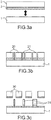
- FIG. 3a Another embodiment of the invention is illustrated on the figures 3a-3b .
- direct bonding of the substrate to be handled 1 is carried out with the handle substrate 2 covered with the bonding layer 3 of porous material.
- the figure 3b one proceeds after direct bonding to a step of cutting the handle substrate 2 to form trenches therefrom isolating regions 20, of the handle substrate from each other. Regions of variable width (5, 10, 20 and 40mm) have thus been isolated. Sealed areas will be created at the edge of each region. So in reference to the figure 3c , annealing at 900 ° C.
- a trench for example annular
- one or more trenches can be made in the substrate to be handled 1. It is then possible to induce a separation of this substrate 1 directly in the form of chips.
Landscapes
- Chemical & Material Sciences (AREA)
- Organic Chemistry (AREA)
- Element Separation (AREA)
- Container, Conveyance, Adherence, Positioning, Of Wafer (AREA)
Description
- Le domaine de l'invention est celui de la réalisation de structures semi-conductrices pour l'électronique, l'optique ou la microélectronique. L'invention porte plus particulièrement sur un procédé de fabrication d'une structure semi-conductrice mettant en œuvre un collage direct temporaire d'un substrat sur un autre.
- Au cours d'un procédé de fabrication d'une structure semi-conductrice, des transferts de couches peuvent être mis en œuvre. Si la couche à transférer est d'épaisseur fine (typiquement inférieure à 200 µm), elle ne peut être manipulée par les moyens classiquement utilisés pour manipuler des substrats sous peine de se fissurer, ou plus généralement d'être endommagée lors de son transfert.
- Un moyen efficace de pallier à ce risque est de renforcer mécaniquement la couche à transférer par un collage temporaire du substrat comprenant la couche à transférer, dit substrat à manipuler, sur un autre substrat, dit substrat poignée. La couche à transférer peut ainsi être librement manipulée et subir toutes les étapes de fabrication nécessaires à son transfert, et plus généralement à son traitement lors d'étapes FEOL (« Front End Of the Line » désignant l'ensemble des étapes de fabrication des composants actifs d'un circuit intégré).
- Le collage temporaire des deux substrats peut être réalisé à l'aide d'une couche adhésive ou bien par collage direct pour former une structure temporaire apte à être soumise à des étapes technologiques de fabrication d'une structure semi-conductrice. Une fois ces étapes réalisées, on procède à la séparation des deux substrats.
- Dans le cas d'un collage au moyen d'une couche adhésive, la séparation des deux substrats comprend un démontage de la structure temporaire réalisé mécaniquement et/ou par l'apport d'un budget thermique permettant la transformation de la couche adhésive. Après séparation, une certaine contamination organique demeure sur les substrats, qui peut être enlevée par nettoyage chimique ou par plasma. Cette succession d'étapes permet de ne pas consommer le substrat poignée. Cependant les matériaux adhésifs, type polymères, peuvent se dégrader et devenir instables sous l'effet de contraintes mécaniques ou thermiques appliquées à la structure temporaire. En particulier, il s'avère quasiment impossible de réaliser des étapes technologiques de fabrication de structures semi-conductrices mettant en œuvre des traitements thermiques dépassant 400 °C.
- Dans le cas d'un collage direct, celui-ci est communément réalisé par collage direct oxyde-oxyde (natif ou thermique) de substrats de silicium. Un recuit de la structure temporaire résultant du collage est généralement réalisé pour qu'un démontage mécanique soit impossible sans risquer d'endommager la couche mince ou le substrat poignée. La séparation de la couche mince du substrat poignée est alors réalisée par élimination du substrat poignée, par exemple par abrasion mécano-chimique. Ce procédé nécessite alors le sacrifice d'un substrat poignée pour chaque couche mince traitée, ce qui représente un coût non négligeable.
- Pour permettre de démonter la structure temporaire, de séparer les deux substrats et rendre possible le recyclage du substrat poignée, des techniques ont été proposées qui consistent à inclure dans l'empilement formant la structure temporaire une ou plusieurs couches pré-fragilisées. Sous l'effet de contraintes mécaniques ou thermiques, ces couches pré-fragilisées sont amenées à se fracturer.
- On connait ainsi une technique consistant à pré-fragiliser le substrat à manipuler en créant au sein de celui-ci une couche poreuse enterrée. Sous l'effet d'un apport externe d'énergie mécanique, cette couche poreuse se fracture. Cette technique est par exemple employée dans le procédé ELTRAN® dont on pourra trouver un descriptif dans l'article « Eltran® ; Novel SOI Wafer Technology », JSAP International. 2001, Vol. 4., de T. Yonehara et S. Koyofumi. Du fait de la fracture au sein du substrat à manipuler, cette technique présente l'inconvénient d'engendrer une perte de matériau. Les résidus de la couche poreuse sont par ailleurs difficiles à retirer par gravure sélective car ils sont constitués du même élément chimique que le substrat. Enfin, les surfaces des substrats séparés sont irrégulières et une étape de polissage mécano-chimique CMP (« Chemical-Mechano Polishing ») s'avère nécessaire, ce qui représente un coût non négligeable. Cette étape a en outre la particularité de consommer une partie du substrat.
- On connait par ailleurs de la demande de brevet
EP 2 977 069 A1 une technique consistant à employer une couche sacrificielle pré-fragilisée à l'interface de collage. Cette couche est pré-fragilisée par implantation ionique et, par un apport thermique, se fracture. Le démontage de la structure intermédiaire s'effectue au niveau de la couche sacrificielle, et non dans l'un des substrats et donc sans perte de matériaux au niveau des substrats. Toutefois, cette technique nécessite elle aussi de réaliser une opération de pré-fragilisation. -
FR 3 002 812 A1 - L'invention concerne un procédé de fabrication d'une structure semi-conductrice mettant en œuvre un collage direct temporaire d'un substrat sur un autre. Elle a pour objectif de fournir un collage qui soit suffisamment résistant pour permettre la réalisation d'étapes technologiques de fabrication de la structure semi-conductrice à haute température (par exemple à 600°C) sans risquer un décollement, et ce au moyen d'un procédé plus simple et moins coûteux que les techniques nécessitant de réaliser une opération de pré-fragilisation d'un substrat ou d'une couche.
- A cet effet, l'invention propose un procédé selon la revendication 1 de fabrication d'une structure semi-conductrice.
- Certains aspects préférés mais non limitatifs de ce procédé sont définis dans les revendications dépendantes.
- D'autres aspects, buts, avantages et caractéristiques de l'invention apparaîtront mieux à la lecture de la description détaillée suivante de formes de réalisation préférées de celle-ci, donnée à titre d'exemple non limitatif, et faite en référence aux dessins annexés sur lesquels :
- les figures la-ld illustrent un premier mode de réalisation du procédé selon l'invention ;
- les
figures 2a-2f illustrent un deuxième mode de réalisation du procédé selon l'invention dans lequel une couche du substrat à manipuler est transférée sur un substrat récepteur; - les
figures 3a-3c illustrent un troisième mode de réalisation du procédé selon l'invention dans lequel le démontage de la structure temporaire conduit à une séparation partielle du substrat poignée ; - la
figure 4 représente la variation de l'énergie de collage en fonction de la température d'un recuit de consolidation appliqué à la structure temporaire. - L'invention a pour objet un procédé de fabrication d'une structure semi-conductrice utilisant un substrat poignée pour supporter un substrat à manipuler.
- On entend par structure semi-conductrice n'importe quelle structure qui est utilisée dans la réalisation d'un dispositif à semi-conducteurs. Une structure semi-conductrice peut comprendre des matériaux conducteurs, semi-conducteurs et/ou des matériaux non conducteurs. Il peut s'agir d'une couche comportant ou non des microcomposants, que ce soient des microcomposants finis ou semi finis.
- On entend par substrat poignée une structure composite dont la fonction est celle de support mécanique temporaire d'un substrat ou d'une structure. Le substrat poignée est par exemple un substrat de silicium.
- On entend par substrat à manipuler un substrat qui est assemblé temporairement à un substrat poignée et sur lequel des traitements peuvent être effectués, en particulier des étapes technologiques FEOL ou BEOL (« Back End Of the Line »). Il peut s'agir par exemple d'un substrat comportant des microcomposants finis ou semi finis à transférer sur un substrat receveur.
- Une description du procédé selon l'invention est tout d'abord donnée en référence aux figures la à 1d qui illustrent un premier mode de réalisation.
- Au cours d'une première étape représentée sur la figure la, on vient déposer sur le substrat poignée 2 une couche de collage 3 en un matériau poreux.
- On procède au cours d'une seconde étape illustrée par la
figure 1b au collage direct du substrat à manipuler 1 avec le substrat poignée 2 par l'intermédiaire de la couche de collage en un matériau poreux 3 recouvrant le substrat poignée. - Par collage direct, on entend un collage par adhésion moléculaire des surfaces mises en contact, sans utilisation d'un matériau spécifique tel qu'une colle. Le collage direct peut être réalisé à température ambiante et à pression atmosphérique. Il peut être précédé d'un traitement préalable des surfaces à coller, par exemple un traitement chimique visant à les rendre hydrophile ou encore un traitement visant à en réduire la rugosité.
- En variante, la couche de collage en matériau poreux peut être déposée sur le substrat à manipuler 1 ou de part et d'autre, à savoir à la fois sur le substrat à manipuler 1 et sur le substrat poignée 2.
- Comme représenté sur la
figure 1b , la couche de collage 3 peut être recouverte d'une couche additionnelle 4 destinée à faciliter le collage, par exemple sous la forme d'une couche superficielle d'oxyde de silicium. De manière similaire, une couche additionnelle 5 peut venir recouvrir le substrat à manipuler 1. - A l'issue du collage direct (
figure 1c ), on obtient une structure temporaire 6 formée par l'empilement du substrat à manipuler 1 assemblé au substrat poignée 2 par l'intermédiaire de la couche de collage 3. - Ce collage est suffisamment résistant pour que la structure temporaire 6 puisse être soumise à des étapes technologiques à haute température (par exemple à 600°C), ce qui est impossible lorsque le collage est assuré au moyen de couches polymères ou métalliques. Ces étapes technologiques peuvent notamment comprendre la formation d'au moins une partie d'un composant micro-technologique et/ou la formation d'au moins une couche isolante.
- Dans un mode de réalisation possible de l'invention, une étape de renforcement du collage peut être mise en œuvre par apport à la structure temporaire 6 d'un budget thermique dit de renforcement. Ce renforcement du collage peut être obtenu par un recuit d'une durée supérieure à 10 minutes à une température dans la gamme 100°C-600°C.
- Ce renforcement est réalisé de manière à permettre la réalisation d'étapes technologiques ultérieures, notamment celles présentant les plus forts budgets thermiques. Le renforcement correspond avantageusement à un premier traitement thermique de la structure intermédiaire, mis en œuvre avant les étapes technologiques ultérieures. Cependant, ces étapes technologiques ultérieures peuvent également participer au budget thermique de renforcement de la tenue mécanique du collage.
- En référence à la
figure 1d , une fois notamment les différentes étapes technologiques réalisées, on procède au démontage de la structure temporaire 6 au niveau de la couche de collage en matériau poreux 3 pour séparer le substrat à manipuler 1 du substrat poignée 2. - Ce démontage est réalisé par apport d'un budget thermique dit de démontage à la structure intermédiaire 6, ledit apport résultant en un démontage spontané, sans application de contrainte mécanique, de la structure temporaire intervenant au niveau de la couche de collage en matériau poreux 3.
- Le démontage peut être réalisé sous atmosphère contrôlée, par exemple pour une couche de collage en matériau organosilicié sous atmosphère d'azote ou une atmosphère mixte N2 et O2, afin de maîtriser la réaction entre cette atmosphère et la couche de collage 3 et ainsi mieux contrôler les conditions de démontage (température plus ou moins haute, durée plus ou moins importante, etc.).
- L'apport du budget thermique de démontage peut prendre la forme d'un recuit réalisé pendant une durée supérieure à 10 minutes à une température supérieure à 600°C. Dans un mode de réalisation possible, il est possible de réunir le budget thermique de renforcement et le budget thermique de démontage en un seul. Ce budget thermique a alors pour rôle de renforcer la tenue mécanique de la structure intermédiaire puis de démonter cette structure.
- Le démontage s'effectue ainsi par fracture au sein de la couche de collage 3 en matériau poreux, et non dans l'un des substrats. Le substrat à manipuler et le substrat poignée ne sont donc pas endommagés.
- On retrouve à l'issue de cette fracture d'un côté le substrat poignée 2 recouvert d'une partie 3' issue de la fracture de la couche de collage 3, et de l'autre le substrat à manipuler également recouvert également d'une partie 3" issue la fracture de la couche de collage 3. Il a pu être observé que ces parties 3', 3" peuvent présenter des épaisseurs identiques, la fracture s'exécutant ainsi au milieu de l'épaisseur de la couche de collage 3. Le substrat poignée 2 peut être facilement recyclé en venant procéder à une étape de recyclage comprenant le retrait des résidus 3' de la couche de collage poreuse présents en surface du substrat poignée à l'issue de l'étape de démontage. Cette étape de retrait présente l'avantage de pouvoir être réalisée par gravure sélective, opération moins coûteuse qu'une opération de CMP. Un retrait des résidus 3" présents sur le substrat à manipuler 1 peut être réalisé de manière similaire par gravure sélective. En variante, une opération de CMP peut être réalisée si on souhaite diminuer la rugosité de surface du matériau poreux (sans l'éliminer totalement) et poursuivre le processus de fabrication du substrat à manipuler.
- On relèvera que ce procédé est plus simple est moins coûteux que les procédés de l'art antérieur. La démontabilité est en effet obtenue par simple dépôt d'une couche unique, et ne nécessite pas d'opération de pré-fragilisation (mécanique, ou par implantation ionique par exemple) à apporter à l'un des substrats ou à la couche de collage.
- La couche de collage en matériau poreux 3 peut être composée d'une matrice inorganique poreuse (métallique, diélectrique, semi-conductrice et plus particulièrement dans les exemples donnés ci-après une matrice comportant des liaisons Si-O) et de composés organiques reliés ou non à la matrice (cycles carbonés, chaines carbonées). Selon l'invention, il s'agit d'une couche poreuse de matériau organosilicié SiOC(H).
- Le choix de cette composition permet le démontage spontané de l'assemblage par un double mécanisme. Sous l'effet d'un traitement thermique, le matériau poreux se densifie en périphérie de plaque créant ainsi une zone scellée en bordure de plaque. Les gaz présents dans le matériau poreux sont alors piégés au sein de la structure temporaire 6. L'expansion de ces gaz piégés avec la température conduit à une fracture spontanée au sein de la couche poreuse.
- Cette couche de collage en matériau poreux présente également la particularité d'évoluer sous l'effet d'un traitement, par exemple un traitement thermique, chimique ou UV. On peut ainsi par un tel traitement ajuster ou créer (dans le cas d'un dépôt via approche porogène) la porosité de la couche de collage. Cette évolution peut être mécanique (par exemple, densification ou modification de l'état de porosité) ou chimique (par exemple, production ou désorption d'espèces gazeuses).
- La couche de collage en matériau poreux 3 peut être déposée par voie physique (exemple : PVD - pour « Physical Vapor Déposition » - et ses dérivées), radicalaire (exemple : sol-gel et ses dérivées), ou encore chimique (exemple : CVD - pour « Chemical Vapor Déposition » - et ses dérivées), et plus particulièrement dans les exemples donnés ci-après par PECVD (« Plasma Enhanced Chemical Vapor Deposition »).
- Une couche de collage en un matériau poreux 3 non utilisée par l'invention peut être une couche à porosité auto-générée par l'encombrement stérique de certains groupements tels que des groupements cycliques (exemple de précurseurs matriciels : triméthyltrivinylcyclotétrasiloxane (V3D3) ou tétraméthylcyclotétrasiloxane (TMCTS)), des groupements méthyles ou dérivés carbonés (exemple de précurseurs matriciels: héxaméthyldisiloxane (HMDSO), bistrisméthylsilylméthane (BTMSM), méthylsilane (1MS), diméthylsilane (2MS), triméthylsilane (3MS), bis (trimethylsiloxy)methylsilane (BTMS), méthyltriméthoxysilane (MTMS)).
- La couche de collage en un matériau poreux 3 selon l'invention peut être une couche à porosité générée par une approche porogène selon laquelle on introduit lors du dépôt de précurseur matriciel des agents porogènes organiques qui sont ensuite retirés par traitement thermique, UV ou par faisceau d'électrons (« e-beam »).
- Les agents porogènes peuvent être chimiquement liés au précurseur matriciel (par exemple : vinyltriméthylsilane (VTMS), divinyldiméthylsilane (DVMS), tétravinylsilane (TVS), diphénylméthylsilane (DPMS)), ou être co-déposés avec le précurseur matriciel (exemples de porogènes : diéthoxyméthylsilane (DEMS), cyclohexène (CHO), décaméthyl-cyclopentasiloxane (DMCPSO), 1-hexène, bicyclohexadiène (BCHD), oxyde de cyclopentène (CPO)).
- Dans les exemples de réalisation donnés ci-après, on procède au co-dépôt par PECVD d'un précurseur matriciel de type methyl-Diethoxy-Silane (MDEOS) et d'agents porogènes de type norbornadiène (NBD) sous flux He et O2. Après retrait des porogènes du co-dépôt, on obtient une couche poreuse à matrice inorganiques Si-O-Si comprenant des groupes méthyles ou dérivés reliés à la matrice par l'atome de silicium (SiO-CH3).
- Le retrait des agents porogènes, réalisé par traitement thermique, UV et/ou e-beam, engendre un taux de porosité variant de 10% à 80% (et plus particulièrement dans les exemples entre 20-30% ±5%) et aussi dans la plupart des cas une contraction d'épaisseur (comprise entre 5% et 25% dans les exemples). Ce retrait peut être réalisé de manière à retirer partiellement ou non les agents porogènes.
- Une ou plusieurs étapes ultérieures peuvent être mises en œuvre afin de modifier la couche poreuse déposée, par exemple afin d'en modifier le taux de porosité, la composition chimique et/ou le taux de porogène restant. Ces étapes consistent par exemple en un traitement thermique, UV ou e-beam supplémentaire, en un traitement chimique (par exemple une gravure HF venant élargir le rayon des pores) ou encore en un traitement plasma. On notera que sous traitement thermique, par exemple, les groupes carbonés (restant de porogènes et/ou groupes méthyles) sont susceptibles de se dégrader sous forme de gaz. Ainsi, le procédé selon l'invention peut comprendre suite au dépôt de la couche de collage en matériau poreux une étape de modification du matériau poreux par post traitement thermique, chimique, UV, faisceau d'électrons ou plasma. Il est ainsi possible, par ingénierie du matériau poreux déposé, de modifier certaines de ses propriétés, et ainsi de modifier la température à laquelle se produit le démontage. La composition et les caractéristiques physico-chimiques du matériau poreux sont donc choisies afin d'adapter le budget thermique de renforcement de la tenue mécanique et de démontage de la structure temporaire.
- Les gaz utilisés au cours du dépôt de la couche poreuse et les gaz dégagés au cours d'un post-traitement de la couche poreuse déposée peuvent être amenés à être piégés dans la couche de collage, par exemple selon la technique de dépôt employée. Ainsi en venant moduler la quantité de gaz produit, on peut venir contrôler le phénomène de démontage. En effet, c'est l'expansion des gaz piégés du fait de la zone scellée en bordure de plaque qui va entraîner le démontage spontané.
- Un exemple de réalisation de l'invention avec deux substrats de silicium (100) de 200 mm dopé P est ci-après détaillé. Le substrat-poignée est recouvert d'une couche de 300 nm de SiO-CH3 poreux par co-dépôt MDEOS+NBD par PECVD sous He et O2. Le retrait des agents porogènes est effectué par traitement UV et thermique qui engendre environ 15%±5% de contraction d'épaisseur. La couche déposée a une composition chimique d'environ 15%±5% de Si, 20%±5% de C et de O, 45%±5% de H et une porosité d'environ 20%±10%. La taille des pores, mesurée par ellipsométrie-porosimétrie, est d'environ 1nm±30%. Le substrat à manipuler est un substrat vierge, non recouvert d'un oxyde thermique. Les deux substrats subissent un traitement chimique ayant pour but de rendre hydrophile les surfaces de silicium et de SiO-CH3 poreux, lequel est réputé pour être très hydrophobe. Ce traitement consiste en un nettoyage chimique de type O3 + RCA. A l'issue de ces différents traitements, la rugosité de surface est de l'ordre de 5 Â RMS (Root Mean Square) pour la couche poreuse déposée de SiO-CH3 et de 1.5 Â RMS pour le substrat à manipuler en silicium, ce qui est compatible avec le collage direct hydrophile. Les deux substrats sont alors collés par la méthode de collage direct à température ambiante et pression atmosphérique pour former la structure dite intermédiaire.
- Cette structure intermédiaire peut alors subir des traitements thermiques jusqu'à 600°C sans décollement. Puis un recuit à plus haute température, à 900°C pendant 2h en atmosphère mixte O2+N2, conduit au démontage de cette structure par fracture au sein de la couche poreuse de SiO-CH3. La fracture est plus particulièrement exécutée au milieu de la couche poreuse comme le révèle des mesures d'épaisseur par ellipsométrie. L'épaisseur de la couche poreuse transférée sur le substrat à manipuler suite à la fracture est d'environ 100 nm±5% et l'épaisseur de la couche poreuse restante sur le substrat poignée est également d'environ 100 nm±5%. Une zone en bord de plaque, correspondant à la zone scellée, est distinguable à l'œil nu. Son épaisseur est de 118nm±5% sur le substrat à manipuler. Après démontage, une rugosité de 1.8 nm RMS est mesurée dans la partie centrale de chacun des substrats.
- Dans un autre exemple de réalisation de l'invention, une découpe de la structure intermédiaire obtenue à l'issue du collage a été réalisée afin d'obtenir des barrettes de collage de largeur 20 mm. Un recuit à 900°C pendant 2h, sous atmosphère mixte O2 + N2, de ces barrettes conduit au démontage par facture au sein du matériau poreux de la couche de collage. Sous atmosphère de N2, le démontage s'opère à 1000°C, soit à une température plus élevée.
- Un autre exemple de réalisation de l'invention est illustré sur les
figures 2a-2f . Il met en œuvre, au moyen de deux collages direct, le transfert d'une couche mince 10' du substrat à manipuler 10 vers un substrat receveur 11. - En référence à la figure la, le substrat-poignée 2 est recouvert d'une couche 3 de 300 mm de SiO-CH3 poreux déposée par PECVD (MDEOS+NBD sous He+O2). Le retrait des agents porogènes est effectué par traitement UV et thermique qui engendre environ 15%±5% de contraction d'épaisseur. La couche déposée a une composition chimique d'environ 15%±5% de Si, 20%±5% de C et de O, 45%±5% de H et une porosité d'environ 20%±10%.
- Le substrat à manipuler 10 est un substrat non fortement dopé qui comprend en surface au moins une partie issue d'étapes FEOL. Les deux substrats 2, 10 sont soumis à un traitement chimique ayant pour but de rendre hydrophile leurs surfaces. Ce traitement consiste en un nettoyage chimique de type O3 + RCA.
- En référence à la
figure 2b , les deux substrats sont collés par la méthode de collage direct à température ambiante et pression atmosphérique. Un premier recuit à 400°C durant 2h est appliquer à la structure intermédiaire 16 afin de consolider et de renforcer mécaniquement l'interface de collage. - En référence à la
figure 2c , un amincissement du substrat à manipuler est effectué sur sa face arrière libre pour former une couche mince 10'. Cet amincissement peut être réalisé par abrasion mécano-chimique ou par mise en œuvre du procédé Smart Cut™ le substrat à manipuler ayant été précédemment soumis à une implantation ionique. - Puis en référence à la
figure 2d , un deuxième collage, hydrophobe, est effectué entre la face arrière libre du substrat à manipuler aminci 10' et un substrat receveur 11. Le substrat receveur est un substrat de silicium dopé non compatible avec l'élaboration de la partie issue d'étapes FEOL présente en surface du substrat à manipuler. - En référence à la
figure 2e , un deuxième recuit est effectué sur l'ensemble de l'empilement issu du deuxième collage à 900°C durant 2h. Ce traitement thermique a pour but de consolider l'interface de collage entre la couche mince 10' et le substrat receveur 11 et de séparer le substrat poignée 2 de la couche mince 2' par fracture au sein de la couche poreuse 3. Ce traitement thermique est réalisé à une température suffisamment peu élevée pour ne pas provoquer une diffusion des dopants trop importante. - Un autre exemple de réalisation de l'invention est illustré sur les
figures 3a-3b . En référence à lafigure 3a , on procède au collage direct du substrat à manipuler 1 avec le substrat poignée 2 recouvert de la couche de collage 3 en matériau poreux. En référence à lafigure 3b , on procède après collage direct à une étape de découpe du substrat poignée 2 pour y former des tranchées venant isoler des régions 20, du substrat poignée les unes des autres. Des régions de largeur variable (5, 10, 20 et 40mm) ont ainsi été isolées. Des zones scellées vont être créées en bordure de chaque région. Ainsi en référence à lafigure 3c , un recuit à 900°C pendant 2h conduit à une séparation partielle du substrat poignée localisée au niveau de régions isolées 20 du substrat poignée, ici les régions présentant une largeur supérieure ou égale à 20mm. Dans les régions de plus petites tailles, la largeur de la zone scellée en bordure de région et la faible quantité de gaz piégé au sein de la région ne permettent pas la séparation spontanée au niveau de cette région. - Cette séparation partielle peut être exploitée pour ne provoquer le démontage que sur une partie centrale de la structure temporaire. Pour ce faire, une tranchée, par exemple annulaire, est réalisée dans le substrat poignée qui vient séparer cette partie centrale d'une partie périphérique du substrat poignée. On obtient alors, éventuellement après un amincissement complémentaire du substrat à manipuler 1, une membrane réalisée dans ce substrat 1 tendue sur la portion périphérique non démontée du substrat poignée, par exemple une portion annulaire.
- De façon similaire, une ou plusieurs tranchées peuvent être réalisées dans le substrat à manipuler 1. Il est alors possible d'induire une séparation de ce substrat 1 directement sous forme de puces.
- On a représenté sur la
figure 4 la variation de l'énergie de collage E, mesurée par la technique d'insertion de lame, en fonction de la température T du recuit de consolidation (ici recuit isotherme pendant deux heures) pour un collage SiO2/Si (en traits pointillés et mesures identifiées par des losanges) et pour un collage Si de porosité initiale de 20% (en traits pleins et mesures identifiées par des triangles). En dessous de la température de démontage TD (autour de 830 °C), l'énergie de collage E s'avère suffisante pour permettre la réalisation de nombreux procédés technologiques à haute température (dépôt de diélectrique, amincissement par exemple). En outre, cette énergie ne s'effondre pas même à l'approche de la température de démontage.
Claims (13)
- Procédé de fabrication d'une structure semi-conductrice, comprenant les étapes de :- collage direct d'un substrat à manipuler (1, 10) avec un substrat poignée (2) par l'intermédiaire d'une couche de collage (3) recouvrant le substrat poignée, pour former une structure temporaire (6, 16) apte à être soumise à des étapes technologiques ; et de- démontage de la structure temporaire au niveau de la couche de collage pour séparer le substrat à manipuler (1, 10) du substrat poignée (2),où le procédé comprend une étape préalable de dépôt de la couche de collage (3) sur le substrat poignée (2) et/ou sur le substrat à manipuler (1), la couche de collage étant une couche poreuse de matériau organosilicié SiOC(H), et où l'étape de démontage est réalisée par apport d'un budget thermique de démontage à la structure intermédiaire (6, 16), ledit apport résultant en un démontage spontané de la structure temporaire intervenant au niveau de la couche de collage.
- Procédé selon la revendication 1, dans lequel l'apport du budget thermique de démontage est réalisé sous atmosphère contrôlée, par exemple une atmosphère d'azote ou une atmosphère mixte N2-O2.
- Procédé selon l'une des revendications 1 et 2, dans lequel l'apport du budget thermique de démontage est un recuit réalisé à une température supérieure à 600°C pendant une durée supérieure à 10 minutes.
- Procédé selon l'une des revendications 1 à 3, comprenant en outre une étape de renforcement du collage mise en œuvre par apport à la structure temporaire (6, 16) d'un budget thermique de renforcement.
- Procédé selon l'une des revendications 1 à 4, comprenant en outre, avant l'étape de démontage, une étape d'assemblage d'une face arrière libre du substrat à manipuler avec un substrat receveur (11).
- Procédé selon l'une des revendications 1 à 5, comprenant en outre une étape de recyclage du substrat poignée comprenant le retrait de résidus (3') de la couche de collage présents en surface du substrat poignée (2) à l'issue de l'étape de démontage au moyen d'une gravure sélective.
- Procédé selon l'une des revendications 1 à 6, dans lequel la couche de collage présente un taux de porosité compris entre 10% et 80%, de préférence entre 15% et 35%.
- Procédé selon l'une des revendications 1 à 7, dans lequel le dépôt de la couche de collage comprend le dépôt d'un précurseur matriciel sur le substrat poignée et l'introduction d'un agent porogène dans le dépôt du précurseur matriciel.
- Procédé selon l'une des revendications 1 à 8, comprenant après le dépôt de la couche de collage une étape de modification de la porosité de la couche de collage par post traitement thermique, chimique, UV, faisceau d'électrons ou plasma.
- Procédé selon l'une des revendications 1 à 9, comprenant, après l'étape de collage direct, la formation d'au moins un tranchée dans le substrat poignée pour isoler des régions (20, 21) du substrat poignée les unes des autres, le démontage de la structure temporaire conduisant à une séparation partielle du substrat poignée localisée au niveau d'au moins une région isolée (20) du substrat poignée.
- Procédé selon la revendication 10, comprenant la formation d'une tranchée dans le substrat poignée venant séparer une partie centrale du substrat poignée d'une partie périphérique du substrat poignée, le démontage de la structure temporaire conduisant à une séparation partielle du substrat poignée localisée au niveau de la partie centrale du substrat poignée, le substrat à manipuler reposant sur la partie périphérique du substrat poignée.
- Procédé selon la revendication 11, comprenant un amincissement du substrat à manipuler reposant sur la partie périphérique du substrat poignée.
- Procédé selon l'une des revendications 1 à 12, comprenant, après l'étape de collage direct, la formation d'une ou plusieurs tranchées dans le substrat à manipuler pour isoler des régions du substrat à manipuler les unes des autres, le démontage de la structure temporaire conduisant à une séparation partielle du substrat à manipuler localisée au niveau d'une ou plusieurs régions isolées du substrat à manipuler.
Applications Claiming Priority (2)
| Application Number | Priority Date | Filing Date | Title |
|---|---|---|---|
| FR1557689A FR3040108B1 (fr) | 2015-08-12 | 2015-08-12 | Procede de fabrication d'une structure semi-conductrice avec collage direct temporaire exploitant une couche poreuse |
| PCT/EP2016/068845 WO2017025494A1 (fr) | 2015-08-12 | 2016-08-08 | Procédé de fabrication d'une structure semi-conductrice avec collage direct temporaire exploitant une couche poreuse |
Publications (2)
| Publication Number | Publication Date |
|---|---|
| EP3335239A1 EP3335239A1 (fr) | 2018-06-20 |
| EP3335239B1 true EP3335239B1 (fr) | 2020-02-12 |
Family
ID=54291500
Family Applications (1)
| Application Number | Title | Priority Date | Filing Date |
|---|---|---|---|
| EP16750789.6A Active EP3335239B1 (fr) | 2015-08-12 | 2016-08-08 | Procédé de fabrication d'une structure semi-conductrice avec collage direct temporaire exploitant une couche poreuse |
Country Status (4)
| Country | Link |
|---|---|
| US (1) | US10643884B2 (fr) |
| EP (1) | EP3335239B1 (fr) |
| FR (1) | FR3040108B1 (fr) |
| WO (1) | WO2017025494A1 (fr) |
Families Citing this family (5)
| Publication number | Priority date | Publication date | Assignee | Title |
|---|---|---|---|---|
| FR3085957B1 (fr) | 2018-09-14 | 2021-01-29 | Commissariat Energie Atomique | Procede de collage temporaire avec adhesif thermoplastique incorporant une couronne rigide |
| FR3088480B1 (fr) | 2018-11-09 | 2020-12-04 | Commissariat Energie Atomique | Procede de collage avec desorption stimulee electroniquement |
| FR3098342B1 (fr) * | 2019-07-02 | 2021-06-04 | Soitec Silicon On Insulator | structure semi-conductrice comprenant une couche poreuse enterrée, pour applications RF |
| WO2021229734A1 (fr) * | 2020-05-14 | 2021-11-18 | 三菱電機株式会社 | Dispositif à semi-conducteur et procédé de fabrication de dispositif à semi-conducteur |
| JP2023550606A (ja) | 2020-11-03 | 2023-12-04 | コーニング インコーポレイテッド | 仮結合プロセスを使用する基板の薄化 |
Family Cites Families (19)
| Publication number | Priority date | Publication date | Assignee | Title |
|---|---|---|---|---|
| US6417069B1 (en) * | 1999-03-25 | 2002-07-09 | Canon Kabushiki Kaisha | Substrate processing method and manufacturing method, and anodizing apparatus |
| JP4538785B2 (ja) * | 2004-03-31 | 2010-09-08 | 和樹 中西 | 有機無機ハイブリッド系多孔質体の製造方法 |
| FR2876220B1 (fr) | 2004-10-06 | 2007-09-28 | Commissariat Energie Atomique | Procede d'elaboration de structures empilees mixtes, a zones isolantes diverses et/ou zones de conduction electrique verticale localisees. |
| US7462552B2 (en) * | 2005-05-23 | 2008-12-09 | Ziptronix, Inc. | Method of detachable direct bonding at low temperatures |
| FR2895419B1 (fr) | 2005-12-27 | 2008-02-22 | Commissariat Energie Atomique | Procede de realisation simplifiee d'une structure epitaxiee |
| FR2895571B1 (fr) * | 2005-12-28 | 2008-04-18 | Commissariat Energie Atomique | Procede de realisation d'une jonction pn electroluminescente en materiau semi-conducteur par collage moleculaire |
| FR2899594A1 (fr) | 2006-04-10 | 2007-10-12 | Commissariat Energie Atomique | Procede d'assemblage de substrats avec traitements thermiques a basses temperatures |
| FR2917235B1 (fr) | 2007-06-06 | 2010-09-03 | Soitec Silicon On Insulator | Procede de realisation de composants hybrides. |
| FR2929447B1 (fr) | 2008-03-28 | 2010-05-28 | Commissariat Energie Atomique | Procede de realisation d'une couche contrainte |
| US8736014B2 (en) * | 2008-11-14 | 2014-05-27 | Taiwan Semiconductor Manufacturing Company, Ltd. | High mechanical strength additives for porous ultra low-k material |
| FR2960340B1 (fr) | 2010-05-21 | 2012-06-29 | Commissariat Energie Atomique | Procede de realisation d'un support de substrat |
| KR20120080926A (ko) * | 2011-01-10 | 2012-07-18 | 삼성전자주식회사 | 다공성 저유전막을 포함하는 반도체 소자의 제조방법 |
| FR2971885A1 (fr) * | 2011-02-18 | 2012-08-24 | Commissariat Energie Atomique | Procédé de réalisation d'un support de substrat |
| FR2977884B1 (fr) | 2011-07-12 | 2016-01-29 | Commissariat Energie Atomique | Procede de realisation d'une structure a membrane suspendue et a electrode enterree |
| FR2977885A1 (fr) | 2011-07-12 | 2013-01-18 | Commissariat Energie Atomique | Procede de realisation d'une structure a electrode enterree par report direct et structure ainsi obtenue |
| FR2982414B1 (fr) | 2011-11-09 | 2014-08-22 | Commissariat Energie Atomique | Procede ameliore de realisation d'un dispositif a cavite formee entre un element suspendu reposant sur des plots isolants semi-enterres dans un substrat et ce substrat |
| FR2987626B1 (fr) * | 2012-03-05 | 2015-04-03 | Commissariat Energie Atomique | Procede de collage direct utilisant une couche poreuse compressible |
| FR3002812B1 (fr) * | 2013-03-01 | 2016-08-05 | St Microelectronics Crolles 2 Sas | Procede de transfert de couche |
| CA2907589C (fr) | 2013-03-18 | 2017-11-21 | Asahi Kasei Medical Co., Ltd. | Matiere de filtre d'elimination d'agregat, procede d'elimination d'agregat, filtre d'elimination de globule blanc et procede de filtration de produit sanguin |
-
2015
- 2015-08-12 FR FR1557689A patent/FR3040108B1/fr not_active Expired - Fee Related
-
2016
- 2016-08-08 EP EP16750789.6A patent/EP3335239B1/fr active Active
- 2016-08-08 US US15/751,043 patent/US10643884B2/en active Active
- 2016-08-08 WO PCT/EP2016/068845 patent/WO2017025494A1/fr not_active Ceased
Non-Patent Citations (1)
| Title |
|---|
| None * |
Also Published As
| Publication number | Publication date |
|---|---|
| EP3335239A1 (fr) | 2018-06-20 |
| US20180358261A1 (en) | 2018-12-13 |
| FR3040108A1 (fr) | 2017-02-17 |
| FR3040108B1 (fr) | 2017-08-11 |
| WO2017025494A1 (fr) | 2017-02-16 |
| US10643884B2 (en) | 2020-05-05 |
Similar Documents
| Publication | Publication Date | Title |
|---|---|---|
| EP2073260B1 (fr) | Procédé de transfer d'une couche mince | |
| EP2004768B1 (fr) | Procede d'assemblage de substrats avec traitements thermiques a basses temperatures | |
| EP1902463B1 (fr) | Procede de diminution de la rugosite d'une couche epaisse d'isolant | |
| EP3335239B1 (fr) | Procédé de fabrication d'une structure semi-conductrice avec collage direct temporaire exploitant une couche poreuse | |
| WO2001093325A1 (fr) | Substrat fragilise et procede de fabrication d'un tel substrat | |
| EP4128329B1 (fr) | Procede de fabrication d'une structure composite comprenant une couche mince en sic monocristallin sur un substrat support en sic | |
| FR2938975A1 (fr) | Procede de realisation d'une heterostructure de type silicium sur saphir | |
| EP4128328B1 (fr) | Procede de fabrication d'une structure composite comprenant une couche mince en sic monocristallin sur un substrat support en sic | |
| WO2009087290A1 (fr) | Procédé de fabrication d'une structure micro-électronique impliquant un collage moléculaire | |
| EP3818561B1 (fr) | Substrat pour un dispositif integre radioafrequence et son procede de fabrication | |
| FR2995136A1 (fr) | Pseudo-substrat avec efficacite amelioree d'utilisation d'un materiau monocristallin | |
| EP4406004A1 (fr) | Procede de fabrication d'un substrat support en carbure de silicium poly-cristallin | |
| WO2021191527A1 (fr) | Procede de fabrication d'une structure empilee | |
| FR3120737A1 (fr) | Procede de fabrication d’une structure semi-conductrice a base de carbure de silicium et structure composite intermediaire | |
| FR3120736A1 (fr) | Procede de fabrication d’une structure semi-conductrice a base de carbure de silicium et structure composite intermediaire | |
| FR2918792A1 (fr) | Procede de traitement de defauts d'interface dans un substrat. | |
| FR2933235A1 (fr) | Substrat bon marche et procede de fabrication associe | |
| FR2928031A1 (fr) | Procede de transfert d'une couche mince sur un substrat support. | |
| EP2979296A1 (fr) | Procede de fabrication d'une structure composite | |
| EP1644969B1 (fr) | Procede d'implantation au travers d'une surface irreguliere | |
| FR2915624A1 (fr) | Procedes de collage et de fabrication d'un substrat du type a couche enterree tres fine. | |
| FR2873235A1 (fr) | Procede d'obtention d'un substrat demontable a energie de collage controlee | |
| EP1861873A1 (fr) | Procede de fabrication d'une hetero-structure comportant au moins une couche epaisse de materiau semi-conducteur | |
| WO2026061720A1 (fr) | Procédé de fabrication d'une structure semi-conductrice à base de carbure de silicium et structure composite intermédiaire | |
| WO2023057700A1 (fr) | Procede de fabrication d'une structure composite comprenant une couche mince en sic monocristallin sur un substrat support en sic poly-cristallin |
Legal Events
| Date | Code | Title | Description |
|---|---|---|---|
| STAA | Information on the status of an ep patent application or granted ep patent |
Free format text: STATUS: THE INTERNATIONAL PUBLICATION HAS BEEN MADE |
|
| PUAI | Public reference made under article 153(3) epc to a published international application that has entered the european phase |
Free format text: ORIGINAL CODE: 0009012 |
|
| STAA | Information on the status of an ep patent application or granted ep patent |
Free format text: STATUS: REQUEST FOR EXAMINATION WAS MADE |
|
| 17P | Request for examination filed |
Effective date: 20180213 |
|
| AK | Designated contracting states |
Kind code of ref document: A1 Designated state(s): AL AT BE BG CH CY CZ DE DK EE ES FI FR GB GR HR HU IE IS IT LI LT LU LV MC MK MT NL NO PL PT RO RS SE SI SK SM TR |
|
| AX | Request for extension of the european patent |
Extension state: BA ME |
|
| DAV | Request for validation of the european patent (deleted) | ||
| DAX | Request for extension of the european patent (deleted) | ||
| STAA | Information on the status of an ep patent application or granted ep patent |
Free format text: STATUS: EXAMINATION IS IN PROGRESS |
|
| 17Q | First examination report despatched |
Effective date: 20190402 |
|
| GRAP | Despatch of communication of intention to grant a patent |
Free format text: ORIGINAL CODE: EPIDOSNIGR1 |
|
| STAA | Information on the status of an ep patent application or granted ep patent |
Free format text: STATUS: GRANT OF PATENT IS INTENDED |
|
| INTG | Intention to grant announced |
Effective date: 20190821 |
|
| GRAJ | Information related to disapproval of communication of intention to grant by the applicant or resumption of examination proceedings by the epo deleted |
Free format text: ORIGINAL CODE: EPIDOSDIGR1 |
|
| STAA | Information on the status of an ep patent application or granted ep patent |
Free format text: STATUS: EXAMINATION IS IN PROGRESS |
|
| GRAR | Information related to intention to grant a patent recorded |
Free format text: ORIGINAL CODE: EPIDOSNIGR71 |
|
| GRAS | Grant fee paid |
Free format text: ORIGINAL CODE: EPIDOSNIGR3 |
|
| STAA | Information on the status of an ep patent application or granted ep patent |
Free format text: STATUS: GRANT OF PATENT IS INTENDED |
|
| INTC | Intention to grant announced (deleted) | ||
| GRAA | (expected) grant |
Free format text: ORIGINAL CODE: 0009210 |
|
| STAA | Information on the status of an ep patent application or granted ep patent |
Free format text: STATUS: THE PATENT HAS BEEN GRANTED |
|
| INTG | Intention to grant announced |
Effective date: 20191220 |
|
| AK | Designated contracting states |
Kind code of ref document: B1 Designated state(s): AL AT BE BG CH CY CZ DE DK EE ES FI FR GB GR HR HU IE IS IT LI LT LU LV MC MK MT NL NO PL PT RO RS SE SI SK SM TR |
|
| REG | Reference to a national code |
Ref country code: GB Ref legal event code: FG4D Free format text: NOT ENGLISH |
|
| REG | Reference to a national code |
Ref country code: CH Ref legal event code: EP |
|
| REG | Reference to a national code |
Ref country code: AT Ref legal event code: REF Ref document number: 1233224 Country of ref document: AT Kind code of ref document: T Effective date: 20200215 |
|
| REG | Reference to a national code |
Ref country code: IE Ref legal event code: FG4D Free format text: LANGUAGE OF EP DOCUMENT: FRENCH |
|
| REG | Reference to a national code |
Ref country code: DE Ref legal event code: R096 Ref document number: 602016029576 Country of ref document: DE |
|
| PG25 | Lapsed in a contracting state [announced via postgrant information from national office to epo] |
Ref country code: FI Free format text: LAPSE BECAUSE OF FAILURE TO SUBMIT A TRANSLATION OF THE DESCRIPTION OR TO PAY THE FEE WITHIN THE PRESCRIBED TIME-LIMIT Effective date: 20200212 Ref country code: NO Free format text: LAPSE BECAUSE OF FAILURE TO SUBMIT A TRANSLATION OF THE DESCRIPTION OR TO PAY THE FEE WITHIN THE PRESCRIBED TIME-LIMIT Effective date: 20200512 Ref country code: RS Free format text: LAPSE BECAUSE OF FAILURE TO SUBMIT A TRANSLATION OF THE DESCRIPTION OR TO PAY THE FEE WITHIN THE PRESCRIBED TIME-LIMIT Effective date: 20200212 |
|
| REG | Reference to a national code |
Ref country code: LT Ref legal event code: MG4D |
|
| REG | Reference to a national code |
Ref country code: NL Ref legal event code: MP Effective date: 20200212 |
|
| PG25 | Lapsed in a contracting state [announced via postgrant information from national office to epo] |
Ref country code: GR Free format text: LAPSE BECAUSE OF FAILURE TO SUBMIT A TRANSLATION OF THE DESCRIPTION OR TO PAY THE FEE WITHIN THE PRESCRIBED TIME-LIMIT Effective date: 20200513 Ref country code: HR Free format text: LAPSE BECAUSE OF FAILURE TO SUBMIT A TRANSLATION OF THE DESCRIPTION OR TO PAY THE FEE WITHIN THE PRESCRIBED TIME-LIMIT Effective date: 20200212 Ref country code: LV Free format text: LAPSE BECAUSE OF FAILURE TO SUBMIT A TRANSLATION OF THE DESCRIPTION OR TO PAY THE FEE WITHIN THE PRESCRIBED TIME-LIMIT Effective date: 20200212 Ref country code: SE Free format text: LAPSE BECAUSE OF FAILURE TO SUBMIT A TRANSLATION OF THE DESCRIPTION OR TO PAY THE FEE WITHIN THE PRESCRIBED TIME-LIMIT Effective date: 20200212 Ref country code: IS Free format text: LAPSE BECAUSE OF FAILURE TO SUBMIT A TRANSLATION OF THE DESCRIPTION OR TO PAY THE FEE WITHIN THE PRESCRIBED TIME-LIMIT Effective date: 20200612 Ref country code: BG Free format text: LAPSE BECAUSE OF FAILURE TO SUBMIT A TRANSLATION OF THE DESCRIPTION OR TO PAY THE FEE WITHIN THE PRESCRIBED TIME-LIMIT Effective date: 20200512 |
|
| PG25 | Lapsed in a contracting state [announced via postgrant information from national office to epo] |
Ref country code: NL Free format text: LAPSE BECAUSE OF FAILURE TO SUBMIT A TRANSLATION OF THE DESCRIPTION OR TO PAY THE FEE WITHIN THE PRESCRIBED TIME-LIMIT Effective date: 20200212 |
|
| PG25 | Lapsed in a contracting state [announced via postgrant information from national office to epo] |
Ref country code: RO Free format text: LAPSE BECAUSE OF FAILURE TO SUBMIT A TRANSLATION OF THE DESCRIPTION OR TO PAY THE FEE WITHIN THE PRESCRIBED TIME-LIMIT Effective date: 20200212 Ref country code: CZ Free format text: LAPSE BECAUSE OF FAILURE TO SUBMIT A TRANSLATION OF THE DESCRIPTION OR TO PAY THE FEE WITHIN THE PRESCRIBED TIME-LIMIT Effective date: 20200212 Ref country code: SM Free format text: LAPSE BECAUSE OF FAILURE TO SUBMIT A TRANSLATION OF THE DESCRIPTION OR TO PAY THE FEE WITHIN THE PRESCRIBED TIME-LIMIT Effective date: 20200212 Ref country code: EE Free format text: LAPSE BECAUSE OF FAILURE TO SUBMIT A TRANSLATION OF THE DESCRIPTION OR TO PAY THE FEE WITHIN THE PRESCRIBED TIME-LIMIT Effective date: 20200212 Ref country code: LT Free format text: LAPSE BECAUSE OF FAILURE TO SUBMIT A TRANSLATION OF THE DESCRIPTION OR TO PAY THE FEE WITHIN THE PRESCRIBED TIME-LIMIT Effective date: 20200212 Ref country code: DK Free format text: LAPSE BECAUSE OF FAILURE TO SUBMIT A TRANSLATION OF THE DESCRIPTION OR TO PAY THE FEE WITHIN THE PRESCRIBED TIME-LIMIT Effective date: 20200212 Ref country code: ES Free format text: LAPSE BECAUSE OF FAILURE TO SUBMIT A TRANSLATION OF THE DESCRIPTION OR TO PAY THE FEE WITHIN THE PRESCRIBED TIME-LIMIT Effective date: 20200212 Ref country code: PT Free format text: LAPSE BECAUSE OF FAILURE TO SUBMIT A TRANSLATION OF THE DESCRIPTION OR TO PAY THE FEE WITHIN THE PRESCRIBED TIME-LIMIT Effective date: 20200705 Ref country code: SK Free format text: LAPSE BECAUSE OF FAILURE TO SUBMIT A TRANSLATION OF THE DESCRIPTION OR TO PAY THE FEE WITHIN THE PRESCRIBED TIME-LIMIT Effective date: 20200212 |
|
| REG | Reference to a national code |
Ref country code: DE Ref legal event code: R097 Ref document number: 602016029576 Country of ref document: DE |
|
| REG | Reference to a national code |
Ref country code: AT Ref legal event code: MK05 Ref document number: 1233224 Country of ref document: AT Kind code of ref document: T Effective date: 20200212 |
|
| PLBE | No opposition filed within time limit |
Free format text: ORIGINAL CODE: 0009261 |
|
| STAA | Information on the status of an ep patent application or granted ep patent |
Free format text: STATUS: NO OPPOSITION FILED WITHIN TIME LIMIT |
|
| 26N | No opposition filed |
Effective date: 20201113 |
|
| PG25 | Lapsed in a contracting state [announced via postgrant information from national office to epo] |
Ref country code: IT Free format text: LAPSE BECAUSE OF FAILURE TO SUBMIT A TRANSLATION OF THE DESCRIPTION OR TO PAY THE FEE WITHIN THE PRESCRIBED TIME-LIMIT Effective date: 20200212 Ref country code: AT Free format text: LAPSE BECAUSE OF FAILURE TO SUBMIT A TRANSLATION OF THE DESCRIPTION OR TO PAY THE FEE WITHIN THE PRESCRIBED TIME-LIMIT Effective date: 20200212 |
|
| PG25 | Lapsed in a contracting state [announced via postgrant information from national office to epo] |
Ref country code: PL Free format text: LAPSE BECAUSE OF FAILURE TO SUBMIT A TRANSLATION OF THE DESCRIPTION OR TO PAY THE FEE WITHIN THE PRESCRIBED TIME-LIMIT Effective date: 20200212 Ref country code: SI Free format text: LAPSE BECAUSE OF FAILURE TO SUBMIT A TRANSLATION OF THE DESCRIPTION OR TO PAY THE FEE WITHIN THE PRESCRIBED TIME-LIMIT Effective date: 20200212 |
|
| PG25 | Lapsed in a contracting state [announced via postgrant information from national office to epo] |
Ref country code: MC Free format text: LAPSE BECAUSE OF FAILURE TO SUBMIT A TRANSLATION OF THE DESCRIPTION OR TO PAY THE FEE WITHIN THE PRESCRIBED TIME-LIMIT Effective date: 20200212 |
|
| REG | Reference to a national code |
Ref country code: CH Ref legal event code: PL |
|
| PG25 | Lapsed in a contracting state [announced via postgrant information from national office to epo] |
Ref country code: CH Free format text: LAPSE BECAUSE OF NON-PAYMENT OF DUE FEES Effective date: 20200831 Ref country code: LU Free format text: LAPSE BECAUSE OF NON-PAYMENT OF DUE FEES Effective date: 20200808 Ref country code: LI Free format text: LAPSE BECAUSE OF NON-PAYMENT OF DUE FEES Effective date: 20200831 |
|
| REG | Reference to a national code |
Ref country code: BE Ref legal event code: MM Effective date: 20200831 |
|
| PG25 | Lapsed in a contracting state [announced via postgrant information from national office to epo] |
Ref country code: IE Free format text: LAPSE BECAUSE OF NON-PAYMENT OF DUE FEES Effective date: 20200808 Ref country code: BE Free format text: LAPSE BECAUSE OF NON-PAYMENT OF DUE FEES Effective date: 20200831 |
|
| PG25 | Lapsed in a contracting state [announced via postgrant information from national office to epo] |
Ref country code: TR Free format text: LAPSE BECAUSE OF FAILURE TO SUBMIT A TRANSLATION OF THE DESCRIPTION OR TO PAY THE FEE WITHIN THE PRESCRIBED TIME-LIMIT Effective date: 20200212 Ref country code: MT Free format text: LAPSE BECAUSE OF FAILURE TO SUBMIT A TRANSLATION OF THE DESCRIPTION OR TO PAY THE FEE WITHIN THE PRESCRIBED TIME-LIMIT Effective date: 20200212 Ref country code: CY Free format text: LAPSE BECAUSE OF FAILURE TO SUBMIT A TRANSLATION OF THE DESCRIPTION OR TO PAY THE FEE WITHIN THE PRESCRIBED TIME-LIMIT Effective date: 20200212 |
|
| PG25 | Lapsed in a contracting state [announced via postgrant information from national office to epo] |
Ref country code: MK Free format text: LAPSE BECAUSE OF FAILURE TO SUBMIT A TRANSLATION OF THE DESCRIPTION OR TO PAY THE FEE WITHIN THE PRESCRIBED TIME-LIMIT Effective date: 20200212 Ref country code: AL Free format text: LAPSE BECAUSE OF FAILURE TO SUBMIT A TRANSLATION OF THE DESCRIPTION OR TO PAY THE FEE WITHIN THE PRESCRIBED TIME-LIMIT Effective date: 20200212 |
|
| PGFP | Annual fee paid to national office [announced via postgrant information from national office to epo] |
Ref country code: DE Payment date: 20250819 Year of fee payment: 10 |
|
| PGFP | Annual fee paid to national office [announced via postgrant information from national office to epo] |
Ref country code: GB Payment date: 20250825 Year of fee payment: 10 |
|
| PGFP | Annual fee paid to national office [announced via postgrant information from national office to epo] |
Ref country code: FR Payment date: 20250827 Year of fee payment: 10 |
|
| REG | Reference to a national code |
Ref country code: DE Ref legal event code: R079 Ref document number: 602016029576 Country of ref document: DE Free format text: PREVIOUS MAIN CLASS: H01L0021762000 Ipc: H10W0010100000 |