EP3306641A1 - Lichtemittierende gasentladungsvorrichtung und ansteuerungsschaltung dafür - Google Patents
Lichtemittierende gasentladungsvorrichtung und ansteuerungsschaltung dafür Download PDFInfo
- Publication number
- EP3306641A1 EP3306641A1 EP16799656.0A EP16799656A EP3306641A1 EP 3306641 A1 EP3306641 A1 EP 3306641A1 EP 16799656 A EP16799656 A EP 16799656A EP 3306641 A1 EP3306641 A1 EP 3306641A1
- Authority
- EP
- European Patent Office
- Prior art keywords
- light
- glass tube
- gas discharge
- emitting
- tube
- Prior art date
- Legal status (The legal status is an assumption and is not a legal conclusion. Google has not performed a legal analysis and makes no representation as to the accuracy of the status listed.)
- Granted
Links
Images


Classifications
-
- H—ELECTRICITY
- H01—ELECTRIC ELEMENTS
- H01J—ELECTRIC DISCHARGE TUBES OR DISCHARGE LAMPS
- H01J61/00—Gas-discharge or vapour-discharge lamps
- H01J61/02—Details
- H01J61/30—Vessels; Containers
- H01J61/35—Vessels; Containers provided with coatings on the walls thereof; Selection of materials for the coatings
-
- H—ELECTRICITY
- H01—ELECTRIC ELEMENTS
- H01J—ELECTRIC DISCHARGE TUBES OR DISCHARGE LAMPS
- H01J61/00—Gas-discharge or vapour-discharge lamps
- H01J61/02—Details
- H01J61/04—Electrodes; Screens; Shields
- H01J61/06—Main electrodes
- H01J61/067—Main electrodes for low-pressure discharge lamps
- H01J61/0672—Main electrodes for low-pressure discharge lamps characterised by the construction of the electrode
-
- C—CHEMISTRY; METALLURGY
- C09—DYES; PAINTS; POLISHES; NATURAL RESINS; ADHESIVES; COMPOSITIONS NOT OTHERWISE PROVIDED FOR; APPLICATIONS OF MATERIALS NOT OTHERWISE PROVIDED FOR
- C09K—MATERIALS FOR MISCELLANEOUS APPLICATIONS, NOT PROVIDED FOR ELSEWHERE
- C09K11/00—Luminescent materials, e.g. electroluminescent or chemiluminescent
- C09K11/08—Luminescent materials, e.g. electroluminescent or chemiluminescent containing inorganic luminescent materials
- C09K11/77—Luminescent materials, e.g. electroluminescent or chemiluminescent containing inorganic luminescent materials containing rare earth metals
- C09K11/7766—Luminescent materials, e.g. electroluminescent or chemiluminescent containing inorganic luminescent materials containing rare earth metals containing two or more rare earth metals
- C09K11/77742—Silicates
-
- C—CHEMISTRY; METALLURGY
- C09—DYES; PAINTS; POLISHES; NATURAL RESINS; ADHESIVES; COMPOSITIONS NOT OTHERWISE PROVIDED FOR; APPLICATIONS OF MATERIALS NOT OTHERWISE PROVIDED FOR
- C09K—MATERIALS FOR MISCELLANEOUS APPLICATIONS, NOT PROVIDED FOR ELSEWHERE
- C09K11/00—Luminescent materials, e.g. electroluminescent or chemiluminescent
- C09K11/08—Luminescent materials, e.g. electroluminescent or chemiluminescent containing inorganic luminescent materials
- C09K11/77—Luminescent materials, e.g. electroluminescent or chemiluminescent containing inorganic luminescent materials containing rare earth metals
- C09K11/7766—Luminescent materials, e.g. electroluminescent or chemiluminescent containing inorganic luminescent materials containing rare earth metals containing two or more rare earth metals
- C09K11/7774—Aluminates
-
- C—CHEMISTRY; METALLURGY
- C09—DYES; PAINTS; POLISHES; NATURAL RESINS; ADHESIVES; COMPOSITIONS NOT OTHERWISE PROVIDED FOR; APPLICATIONS OF MATERIALS NOT OTHERWISE PROVIDED FOR
- C09K—MATERIALS FOR MISCELLANEOUS APPLICATIONS, NOT PROVIDED FOR ELSEWHERE
- C09K11/00—Luminescent materials, e.g. electroluminescent or chemiluminescent
- C09K11/08—Luminescent materials, e.g. electroluminescent or chemiluminescent containing inorganic luminescent materials
- C09K11/77—Luminescent materials, e.g. electroluminescent or chemiluminescent containing inorganic luminescent materials containing rare earth metals
- C09K11/7766—Luminescent materials, e.g. electroluminescent or chemiluminescent containing inorganic luminescent materials containing rare earth metals containing two or more rare earth metals
- C09K11/778—Borates
-
- H—ELECTRICITY
- H01—ELECTRIC ELEMENTS
- H01J—ELECTRIC DISCHARGE TUBES OR DISCHARGE LAMPS
- H01J61/00—Gas-discharge or vapour-discharge lamps
- H01J61/02—Details
- H01J61/30—Vessels; Containers
- H01J61/302—Vessels; Containers characterised by the material of the vessel
-
- H—ELECTRICITY
- H01—ELECTRIC ELEMENTS
- H01J—ELECTRIC DISCHARGE TUBES OR DISCHARGE LAMPS
- H01J61/00—Gas-discharge or vapour-discharge lamps
- H01J61/02—Details
- H01J61/30—Vessels; Containers
- H01J61/305—Flat vessels or containers
-
- H—ELECTRICITY
- H01—ELECTRIC ELEMENTS
- H01J—ELECTRIC DISCHARGE TUBES OR DISCHARGE LAMPS
- H01J61/00—Gas-discharge or vapour-discharge lamps
- H01J61/02—Details
- H01J61/30—Vessels; Containers
- H01J61/33—Special shape of cross-section, e.g. for producing cool spot
-
- H—ELECTRICITY
- H01—ELECTRIC ELEMENTS
- H01J—ELECTRIC DISCHARGE TUBES OR DISCHARGE LAMPS
- H01J61/00—Gas-discharge or vapour-discharge lamps
- H01J61/02—Details
- H01J61/56—One or more circuit elements structurally associated with the lamp
-
- H—ELECTRICITY
- H01—ELECTRIC ELEMENTS
- H01J—ELECTRIC DISCHARGE TUBES OR DISCHARGE LAMPS
- H01J61/00—Gas-discharge or vapour-discharge lamps
- H01J61/92—Lamps with more than one main discharge path
-
- H—ELECTRICITY
- H01—ELECTRIC ELEMENTS
- H01J—ELECTRIC DISCHARGE TUBES OR DISCHARGE LAMPS
- H01J65/00—Lamps without any electrode inside the vessel; Lamps with at least one main electrode outside the vessel
-
- H—ELECTRICITY
- H01—ELECTRIC ELEMENTS
- H01J—ELECTRIC DISCHARGE TUBES OR DISCHARGE LAMPS
- H01J65/00—Lamps without any electrode inside the vessel; Lamps with at least one main electrode outside the vessel
- H01J65/04—Lamps in which a gas filling is excited to luminesce by an external electromagnetic field or by external corpuscular radiation, e.g. for indicating plasma display panels
- H01J65/042—Lamps in which a gas filling is excited to luminesce by an external electromagnetic field or by external corpuscular radiation, e.g. for indicating plasma display panels by an external electromagnetic field
- H01J65/046—Lamps in which a gas filling is excited to luminesce by an external electromagnetic field or by external corpuscular radiation, e.g. for indicating plasma display panels by an external electromagnetic field the field being produced by using capacitive means around the vessel
-
- H—ELECTRICITY
- H05—ELECTRIC TECHNIQUES NOT OTHERWISE PROVIDED FOR
- H05B—ELECTRIC HEATING; ELECTRIC LIGHT SOURCES NOT OTHERWISE PROVIDED FOR; CIRCUIT ARRANGEMENTS FOR ELECTRIC LIGHT SOURCES, IN GENERAL
- H05B33/00—Electroluminescent light sources
- H05B33/12—Light sources with substantially two-dimensional [2D] radiating surfaces
- H05B33/14—Light sources with substantially two-dimensional [2D] radiating surfaces characterised by the chemical or physical composition or the arrangement of the electroluminescent material, or by the simultaneous addition of the electroluminescent material in or onto the light source
Definitions
- the present invention relates to a gas discharge light-emitting device and a drive circuit therefor, and more particularly to a novel ultraviolet light-emitting device which has an external electrode structure including a thin glass tube as a main component and which uses a gas discharge, and a drive circuit therefor.
- Patent Document 1 a gas discharge light-emitting device using an ultraviolet light-emitting phosphor is disclosed in Patent Document 1, and a gas discharge light-emitting device having a thin tube configuration suitable for a configuration of a flat light source has been proposed in, for example, Patent Documents 2 and 3.
- Patent Document 1 discloses an excimer discharge lamp configuration using an ultraviolet phosphor of UV-C band.
- this configuration has problems of requiring an expensive quartz glass envelope and requiring a high-voltage rectangular-wave alternating-current power supply for drive.
- gas discharge devices for ultraviolet light emission using a gas discharge tube disclosed in Patent Documents 2 and 3 have a complicated electrode structure, and have not yet been developed to a practical level from a viewpoint of luminous efficiency and emission intensity.
- the present inventors have invented a novel gas discharge light-emitting device comprising a pair of long electrodes which is provided outside of a thin glass tube filled with a discharge gas and extends in a direction away each other from a gap interposed between adjacent ends of the electrodes (see, PCT/JP2016/052716 ).
- this gas discharge light-emitting device high efficient light emission throughout the entire length of an electrode arrangement region can be obtained by driving through application of a sine wave voltage between the pair of long electrodes .
- This plasma tube type gas discharge light-emitting device operates such that a trigger discharge is initially generated between adjacent ends of the electrodes during an increasing process of a sine wave voltage applied between both electrodes, and this trigger discharge is gradually grown so as to expand in longitudinal direction of the electrodes until the applied voltage reaches a peak value.
- the present inventors have experienced, in an operating test for a gas discharge device provided with a pair of long electrodes according to the previous invention, a phenomenon in which an unnecessary spark discharge occurs along the side edges of the long electrodes outside the tube.
- the device when the device is driven by applying a sine wave voltage to one of a pair of long electrodes with the other being grounded, it is considered that, at the stage at which the applied voltage reaches a peak value, the inside of the tube is substantially in a conductive state due to a plasma throughout the entire length to have a potential corresponding to the peak voltage, and an unexpected spark discharge occurs in a gap between the curved surface of the tube and the side edge of the electrode having a ground potential, which face each other.
- even when air bubbles are present on a contact surface between the outer wall surface of the tube and the long electrodes due to fine irregularities on the outer wall surface of the tube there is a risk of a spark discharge being caused at the portion where air bubbles are present.
- the spark discharge outside the tube causes generation of unpleasant ozone and damage on the electrode or the tube, and thus, not preferable from the viewpoint of safety.
- the present invention is accomplished in view of the above circumstances, and aims to provide: a gas discharge light-emitting device for a light source, particularly for an ultraviolet light source, that has a simple configuration, is inexpensive, and has excellent emission efficiency, and that can prevent particularly a spark discharge on a wall surface outside a tube; and a drive circuit therefor.
- the present invention also aims to provide a gas discharge light-emitting device for a flat light source, particularly for an ultraviolet flat light source, which can be easily formed into a module to which a drive circuit is integrated and can provide light emission with high efficiency and high intensity with a compact size.
- the present invention is characterized by a configuration in which a discharge electrode is provided on the outer wall surface of a glass tube through an insulating layer.
- the present invention is based on an idea in which an electric field from a plasma, in the tube, which causes a spark discharge is weakened by the insulating layer desposed between the discharge electrode and the outer wall surface of the tube to prevent the spark discharge along the outer wall surface of the tube.
- the first aspect of the present invention lies in the configuration of a gas discharge light-emitting device comprising: a glass tube, as a main component, filled with a discharge gas and having a front side upper part and a back side bottom part which face each other on a transverse section thereof; at least a pair of discharge electrodes provided on an outer wall surface of the glass tube so as to extend along the longitudinal direction of the tube to be away from each other; and an insulating layer disposed between the glass tube and the discharge electrodes with width wider than a width of the transverse section of the glass tube.
- An insulating film can be used for the insulating layer interposed between the outer surface of the glass tube and the discharge electrodes.
- the pair of discharge electrodes is configured to extend along the longitudinal direction of the glass tube in a direction away from each other from a trigger discharge gap which is formed between adjacent ends of the discharge electrodes, and is formed by pasting a metal foil in a solid pattern on the insulating layer on the back side of the glass tube.
- a light source for ultraviolet light emission can be obtained by providing an ultraviolet phosphor layer on the inner surface of the bottom part on the back side.
- this light source if a light-emitting surface on the front side of the glass tube is thin with a thickness of 300 ⁇ m or less, preferably 100 ⁇ m or less, transmittance of 80% or higher with respect to ultraviolet light with UV-C and UV-B wavelength bands is achieved, even when inexpensive borosilicate glass is used as the glass material. Thus, this light source has no problem in practical use.
- the second aspect of the present invention lies in a configuration of a flat light source unit comprising: a plurality of gas discharge light-emitting tubes which is arranged parallel to one another to form a tube array, each of the gas discharge light-emitting tubes having, as a main component, a glass tube filled with a discharge gas and having an upper part and a bottom part facing each other on a transverse section thereof with the upper part being defined as a light-emitting surface and the bottom part being provided with a phosphor layer on an inner surface thereof; and a pair of discharge electrodes formed from a metal foil conductor and commonly provided on the back side of the tube array through an insulating film.
- the pair of discharge electrodes which is commonly provided has a pattern of the long electrodes extending along the longitudinal direction of each glass tube in a direction away from each other from a gap formed between the adjacent ends of the electrodes.
- Respective tube structure in this flat light source is substantially the same as the configuration of the above-mentioned gas discharge light-emitting tube as a unit light source.
- a flat light source unit for ultraviolet light emission can be obtained by providing an ultraviolet light-emitting phosphor layer on the bottom inner surface of each tube.
- the third aspect of the present invention lies in a configuration of a drive circuit for driving a plasma tube
- a drive circuit for driving a plasma tube comprising: a glass tube, as a main component, filled with a discharge gas and having a front upper part and a back bottom part which face each other on a transverse section thereof; and at least a pair of discharge electrodes provided on an outer wall surface of the glass tube through an insulating layer so as to extend along a longitudinal direction of the glass tube to be away from each other, wherein one of output terminals of a secondary winding of a step-up transformer that generates an alternating voltage to be applied is connected to one of the pair of discharge electrodes together with a reference potential, and another one of alternating voltage output terminal of the secondary winding is directly connected to the other electrode.
- a current limiting capacitor is connected to an output side of a step-up transformer in a power supply circuit.
- the gas discharge device of an external electrode type according to the present invention is completely a capacitive load, so that it has a function for automatically stopping a discharge current due to accumulation of wall charges on the inner wall surface of the glass tube caused by the discharge. Therefore, the output capacitor can be eliminated, and the output voltage from the step-up transformer can be directly applied to the pair of discharge electrode for driving the plasma tube. Thus, unnecessary power loss caused by the output capacitor in the step-up circuit can be eliminated.
- the main constituent features of the gas discharge light-emitting device according to the present invention are the glass tube, the phosphor layer provided inside the glass tube, and the discharge gas filled in the glass tube, so that the gas discharge light-emitting device does not contain toxic mercury.
- a pair of long discharge electrodes provided on the outer surface of the glass tube so as to extend along the longitudinal direction to be away from each other with a discharge gap being formed therebetween is simple, and according to the pair of long discharge electrodes, uniform light emission with high-efficient and high-intensity can be achieved throughout the entire length of the glass tube.
- the insulating layer being interposed between the discharge electrodes and the outer surface of the glass tube provides an effect of preventing a spark discharge along the side edge of the electrodes.
- a drive circuit unit including, as a main component, a printed substrate serving also as a support substrate is integrally mounted below the common electrodes, which allows the light source to be constructed into a module.
- a flat light source module high-efficient and high-intensity surface light emission can be achieved, and further, this module can be handled with safety because no spark discharge occurs.
- the flat light source module for ultraviolet light emission constructed by using an array of multiple gas discharge light-emitting tubes particularly provided with an ultraviolet light-emitting phosphor layer can be constructed not only to include no mercury but also to be capable of performing uniform and high-intensity ultraviolet radiation from a wide light-emitting surface without causing shadows, thereby providing an effect of expanding practical application for medical use or industrial use.
- FIGS. 1(a) and 1(b) are each a schematic longitudinal sectional view and a transverse sectional view showing the basic configuration of a gas discharge light-emitting device according to the present invention as a first embodiment.
- An elongate glass tube 1 filled with a gaseous mixture of neon (Ne) and xenon (Xe) as a discharge gas constitutes an envelope that is a main component of the device.
- the glass tube 1 has a transverse section with a flat-oval shape, and has a front side upper part 1a and a back side bottom part 1b which are flat and face each other across a major axis.
- a pair of discharge electrodes 3 and 4 extending along the longitudinal direction of the glass tube 1 is arranged to extend to either side with an electrode gap 5 being interposed between adjacent ends thereof on the outer surface of the glass tube 1 on the back side bottom part through an insulating layer 2.
- the discharge electrodes 3 and 4 are elongate along the glass tube 1, so that they are referred to as long electrodes.
- the glass tube 1 which is a main component is formed such that a pipe-like preform of a borosilicate glass including silicon oxide (SiO 2 ) and boron oxide (B 2 O 3 ) as main components is redrawn to be formed into a thin tube with an outer diameter of 0.5-5 mm and a thickness of 500 ⁇ m or less.
- the glass tube 1 has a transverse section with a flat-oval shape with a major axis of 2 mm and a minor axis of 1 mm as shown in FIG. 1(b) .
- the glass tube 1 may have a transverse section with any shape such as a circle, rectangle, oblong, or trapezoid.
- the insulating layer 2 which is the feature of the present invention is formed from an insulating tape or an insulating film affixed on the flat surface of the back side bottom part 1b of the glass tube 1 with a width larger than the major axis of the glass tube.
- the insulating layer 2 preferably has a thickness of 50-200 ⁇ m. If the insulating layer 2 is too thin, a function of preventing an external discharge is insufficient, and if it is too thick, it is difficult to obtain sufficient discharge expansion in the tube in relation to a discharge voltage.
- a heat-resistant tape or film made of a polyimide resin can be used for the insulating layer 2.
- Kapton tape (trade name) can preferably be used.
- a pair of long electrodes 3 and 4 is arranged on the lower surface of the insulating layer 2 as described later.
- An ultraviolet light-emitting phosphor layer 6 is formed on the inner surface of the glass tube 1 on the back side bottom part 1b.
- This ultraviolet light-emitting phosphor layer 6 is excited by vacuum ultraviolet light (emission wavelength: 143 nm, 173 nm) generated by a gas discharge using a gaseous mixture of neon and xenon, thereby generating ultraviolet light or visible light having spectrum according to the characteristics of the phosphor.
- UV-B band having a peak wavelength with a narrow bandwidth at 311 nm can be obtained.
- UV emission of UV-C band having a peak wavelength at 263 nm can be obtained.
- the gas discharge light-emitting tube (plasma tube 10) for an ultraviolet light source is constructed by forming the ultraviolet light-emitting phosphor layer 6, it is important to set the thickness of the front side upper part 1a, serving as a light-emitting surface, of the glass tube 1 to be 300 ⁇ m or less from the viewpoint of the ultraviolet transmittance.
- the present inventors have proved through experiments that, even if borosilicate glass such as Pyrex (registered trademark) is used, transmittance of 90% or more with respect to ultraviolet light having the UV-B wavelength band can be obtained by adjusting the thickness to be 300 ⁇ m or less.
- the thickness of the light-emitting surface is set to be 100 ⁇ m or less, transmittance of 80% or more even with respect to ultraviolet light having the UV-C wavelength band can be obtained.
- the thickness at the back side bottom part 1b of the glass tube 1 where the insulating layer 2, the long electrodes 3 and 4, and the ultraviolet light-emitting phosphor layer 6 are disposed may be set larger than the thickness at the front side upper part 1a to enhance mechanical strength.
- the glass tube 1 in which the thicknesses of the surfaces facing each other are asymmetric can be implemented by a process control for shaping the glass preform.
- adjacent proximal ends of a pair of long electrodes 3 and 4 arranged on the insulating layer 2 constitute trigger electrode portions 3a and 4a with the electrode gap 5 interposed therebetween, and a gas space corresponding to the electrode gap 5 becomes a trigger discharge portion 7.
- extension portions extending to either side from the trigger electrode portions 3a and 4a in the direction away from each other constitute main electrode portions 3b and 4b, and a gas space corresponding to the main electrode portions 3b and 4b becomes a main gas discharge portion 8.
- a pair of long electrodes 3 and 4 having the trigger electrode portions 3a and 4a and the main electrode portions 3b and 4b are respectively referred to as the X electrode 3 and the Y electrode 4 below.
- An electrode gap length Dg of the electrode gap 5 is set within the range of 0.1-20 mm, as appropriate.
- the X electrode 3 and the Y electrode 4 are set to have a length more than three times to about ten times or more than the electrode gap length Dg.
- the arrangement of a pair of long electrodes enables uniform light emission throughout the entire length of the light-emitting tube.
- the electrode gap length Dg is set to be 3 mm, and the X electrode 3 and the Y electrode 4 each have a length of 23.5 mm, the gas discharge light-emitting tube 10 having an effective light-emitting region with a length of 50 mm is obtained based on the total size. It is to be noted that the length of the X and Y electrodes 3 and 4 that make a pair needs to be determined in consideration of the relationship between the peak value of an alternating drive voltage necessary for expanding the discharge throughout the entire length of the effective light-emitting region and the breakdown voltage of the electrode gap 5.
- the X electrode 3 and the Y electrode 4 may be directly formed on the lower surface of the insulating film 2, which is affixed on the outer surface 1b of the bottom part of the plasma tube 10, by printing conductive ink such as a silver paste or the like in advance, or may be formed by pasting or bonding a metal conductive foil such as a copper foil or an aluminum foil onto the lower surface of the insulating film 2.
- conductive ink such as a silver paste or the like
- a metal conductive foil such as a copper foil or an aluminum foil onto the lower surface of the insulating film 2.
- an electrode substrate on which a metal conductive film having an electrode pattern is formed by printing or vapor deposition is prepared, and this electrode substrate can be pasted on the surface of the back side bottom part 1b of the plasma tube 10 through a base film serving as the insulating layer.
- the X and Y electrodes are preferably formed from a material having high light reflection characteristic, and for this point, it is effective to use an aluminum foil in particular.
- the electrode gap 5 may be a window open downward relative to the non-transmissive part of the X and Y electrodes 3 and 4, so that emitted light exits to the back side, which may cause unevenness in an emission intensity distribution on the light-emitting surface. Therefore, when the insulating layer 2 is formed from a material having light transparency, it is preferable that at least the electrode gap 5 is closed by an insulating material having light reflection characteristic equal to the light reflection characteristic of the electrode material, such as a reflection tape.
- this transparent coating layer can be functioned as the electrode insulating layer 2.
- this transparent coating layer can be functioned as the electrode insulating layer 2.
- resistance to weather and mechanical strength of the glass tube are enhanced by Teflon coating, and further, irregularities on the surface of the glass tube 1 are absorbed by Teflon coating, whereby air bubbles being present on the contact surface between the glass tube 1 and the electrodes can be eliminated to prevent a spark discharge.
- a pair of translucent electrodes may be arranged on the front side of the glass tube.
- the gas discharge light-emitting tube of a novel type according to the present invention that is, the plasma tube 10
- has an external electrode type and is driven by a sine wave voltage.
- a sine wave voltage is applied to the Y electrode 4 of the pair of X and Y electrodes 3 and 4 with the X electrode 3 being grounded, a trigger discharge is generated at a point at which the voltage between the trigger electrode portions 3a and 4a exceeds a discharge start voltage of the trigger discharge portion 7 during an increasing process of the voltage.
- the sine wave drive voltage is set such that the discharge is expanded to either end of the X electrode 3 and the Y electrode 4 at its peak value.
- the length of the X electrode 3 and the Y electrode 4 is determined such that the peak value of the sine wave drive voltage does not exceed the breakdown voltage of the electrode gap 5.
- the driving frequency is a factor for determining an emission intensity, and is appropriately set to several 10 kHz, for example, 40 kHz.
- the risk of a spark discharge generated in the gap between the electrodes and the both side edges of the curved surface portion on the bottom part of the plasma tube 10 can be avoided by the wide insulating film 2.
- the electrodes are not directly exposed on portions facing the curved surface portions at both side edges on the bottom part of the tube, whereby the electric field in the gap at said both side edges is not increased enough to cause the spark discharge.
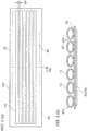
- FIGS. 2(a) and 2(b) each show a schematic plan view and a transverse sectional view of a gas discharge light-emitting device according to a second embodiment of the present invention.
- the gas discharge light-emitting device according to the second embodiment is characterized by a configuration of a flat surface light source unit 100 of a light emitting tube array type in which a plurality of gas discharge light-emitting tubes (plasma tubes) 10 is arrayed parallel to one another.
- an adhesive agent having excellent thermal conductivity such as silicon grease, is used to fix the tubes 10 on the insulating film 20. Due to the space SP between the adjacent tubes being filled with the adhesive agent, a spark discharge along the outer walls of the tubes can reliably be prevented. If a large number of gas discharge light-emitting tubes 10 are arrayed, several tubes may be collected as a unit block, and a space SP may be formed between the adjacent unit blocks. Due to the space SP being formed, the flat light source unit 100 has flexibility in the arraying direction of the gas discharge light-emitting tubes 10.
- the flat surface light source unit 100 has a configuration of a tube array in which six gas discharge light-emitting tubes 10 are supported parallel to one another on the common insulating film 20.
- An X electrode 30 and an Y electrode 40 formed from a metal conductive film or foil are disposed on the lower surface of the insulating film 20 so as to be common to the respective gas discharge light-emitting tubes 10 with a gap having a length Dg therebetween across the respective tubes at almost the center thereof.
- the X electrode 30 and the Y electrode 40 each have a pattern for covering almost the entire region of the tube array at the back side except for the gap Dg as shown in FIG.
- the insulating film 20 is formed from the Kapton tape (trade name) mentioned above, and the electrodes 30 and 40 are formed from an aluminum foil.
- the X electrode 30 and the Y electrode 40 formed from an aluminum foil are pasted on the back surface of the Kapton tape with a bonding agent or an adhesive agent. It should be noted that the X electrode 30 and the Y electrode 40 made of an aluminum foil are preferably formed to have a dimensional pattern such that ends thereof are slightly inward from both ends of the gas discharge light-emitting tubes 10 to avoid a risk of contact therebetween.
- the insulating film 20 having a function as a support member for the gas discharge light-emitting tubes 10 has a thickness of about 50 to 100 ⁇ m, and the aluminum foil constituting the X electrode 30 and the Y electrode 40 has a thickness of about 10 ⁇ m.
- FIG. 2 shows a principled configuration of the flat light source unit 100 according to the present invention, and it is not preferable to use the unit 100 with the X electrode 30 and the Y electrode 40 being directly exposed on the lower surface of the unit 100.
- the surface where the X electrode and the Y electrode are disposed is covered by another insulating film which is not shown.
- a printed electrode substrate having formed thereon a conductive film with an electrode pattern with printing or vapor deposition is formed on another insulating substrate not shown, and the gas discharge tubes 10 supported on the insulating film 20 are overlaid on this insulating substrate.
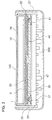
- FIG. 3 is a schematic sectional view of a gas discharge light-emitting device having a drive-circuit-integrated light source module configuration according to a third embodiment.
- the flat light source unit 100 described in the second embodiment is overlaid on a printed substrate 26 constituting a drive circuit unit 200 through an impact absorbing layer 25, and they are integrally stored in an external frame or a case 27. Further, a translucent protection plate 28 is provided on the front surface of the flat light source unit 100.
- a soft insulating material having high thermal conductivity and impact absorption property such as a silicon compound or a silicon sheet, is preferable for the impact absorbing layer 25.
- An acrylic or fluoroplastic film or thin plate having excellent ultraviolet light transmittance is used for the protection plate 28.
- the printed substrate 26 has mounted thereon components of the drive circuit unit 200 described later.
- a pair of power feed terminals 31 and 41 which is brought into contact with the X electrode 30 and the Y electrode 40 on the back surface of the flat light source unit 100 is provided on the left and right sides on the top surface of the printed substrate 26.
- the contact between the X electrode 30 and the power feed terminal 31 and between the Y electrode 40 and the power feed terminal 41 does not require DC connection in a strict sense, and an alternate drive voltage can be supplied to the flat light source unit 100 from the drive circuit unit 200 only by bringing the electrode and the corresponding terminal into a touch state where they only overlap each other directly or through a clip-shaped contact piece. Therefore, the light source unit 100 and the drive unit 200 can easily be separated from each other.
- the drive circuit unit 200 generates a sine wave drive voltage to drive the flat light source unit 100.
- the sine wave drive voltage is supplied to the Y electrode 40 from the power feed terminal 41 with the power feed terminal 31 defined as a ground being connected to the X electrode 30, whereby the discharge light emission with the operation principle described previously can be obtained.
- the flat light source unit 100 with an emission area of 90 cm 2 can be obtained by arranging, with an interval of 1 mm, thirty(30) gas discharge light-emitting tubes 10 having a flat-oval cross-sectional shape with a major axis of 2 mm and a minor axis of 1 mm and having an effective emission area with a length of 10 cm.
- the diameter of the gas discharge light-emitting tube 10 is a maximum of 5 mm, and the total thickness of the light source module including the impact absorbing layer 25, the printed substrate 26, and the protection plate 28 on the front surface as well as the gas discharge light-emitting tube 10 is 1 cm or less.
- an alternating-voltage drive circuit having a peak voltage of several 1000 V and a frequency of several 10 kHz is needed.
- the light source unit has only about thirty light-emitting tubes, it can beneficially be driven by a later-described popular compact power source with about several Watts.
- the drive circuit unit including the battery may have a size within a capacity of about 50 cm 3 .
- the storage case 27 only requires a compact size of 9 x 10 cm with a thickness of about 1 cm.
- FIG. 4 is a circuit diagram showing one example of a circuit structure of the drive circuit unit 200.
- a battery BT to which a voltage can be set within a range of DC 6-18 V is connected to an inverter circuit section INV through an input plug PL1.
- the inverter circuit section INV is composed of transistors Q1 and Q2, a coil L1, resistors R1 and R2, and a capacitor C1.
- An alternating output from the inverter circuit section INV is extracted from an output plug PL2 from a secondary winding of a step-up transformer TF.
- a sine wave alternating high voltage is obtained at the output plug PL2 by appropriately setting the circuit constant of each circuit component, and the obtained voltage is applied between the X electrode 30 and the Y electrode 40 of the gas discharge light-emitting tubes 10.
- the drive circuit unit 200 can cause the gas discharge light-emitting tube 10 to emit light through application of the similar voltage to the X electrode 3 and the Y electrode 4 in the first embodiment.
- the frequency of the sine wave voltage can be adjusted within a range of 10 kHz to 80 kHz by varying the capacitance of the capacitor C1, and the peak value of the sine wave output voltage can be adjusted within the range of 1000 V to 8000 V by varying the voltage of the battery BT.
- the drive circuit shown in FIG. 4 is that there is no current limiting capacitor which is generally provided on an output line of the step-up transformer TF.
- One of the output lines of the step-up transformer is connected to a ground potential and the grounded X electrode 3 or 30 of the gas discharge tube 10, and the other output line is directly connected to the Y electrode 4 or 40.
- the gas discharge tube 10 according to the present invention becomes a complete capacitive load relative to the drive circuit unit 200, whereby unnecessary power loss can be eliminated by eliminating an output capacitor.
- the printed substrate 26 has mounted thereon circuit components 47, such as a coil, a capacitor, and a transformer, that constitute the drive circuit.
- the printed substrate 26 is disposed on the lower part of the light source unit 100 with the mounted components facing downward.
- the battery BT serving as a power supply may be stored in a battery storage unit formed in the case 27, or may be connected to an external power supply by a power supply connection line led from the printed substrate 26.
- gas discharge light-emitting device for ultraviolet light emission has been mainly described above, a visible light source using a phosphor which is excited by vacuum ultraviolet light due to gas discharge to emit light in a visible region can also be implemented.
- the gas discharge light-emitting device according to the present invention is also usable as a light source which uses light emission, in an ultraviolet region or a visible region, by a gas discharge itself without using a phosphor.
- the gas discharge light-emitting tube serving as a light emission unit is thin with a diameter of several millimeters. Therefore, in the configuration of the flat light source unit 100 shown in FIG. 2 , a common flexible support substrate (not shown) is additionally provided, and the light source unit 100 is disposed on this substrate through an adhesive layer or a buffer layer, by which the exposure of the X electrode and the Y electrode can be prevented, and the support strength can be increased.
- the number of the light-emitting tubes 10 to be arrayed can be increased, and the length of the light-emitting tubes can be increased, which lead to an increase in a light-emitting surface as appropriate.
- the large-scale flat light source unit has a film shape with flexibility, thereby providing a benefit of easily obtaining a curved light-emitting surface for medical use or sterilization use.
- multiple electrode pairs for each light-emitting tube are provided on a common insulating layer as segment electrode pairs common to all of the light-emitting tubes in the direction crossing the light-emitting tubes.
Landscapes
- Chemical & Material Sciences (AREA)
- Engineering & Computer Science (AREA)
- Inorganic Chemistry (AREA)
- Materials Engineering (AREA)
- Organic Chemistry (AREA)
- Physics & Mathematics (AREA)
- Plasma & Fusion (AREA)
- Electromagnetism (AREA)
- Vessels And Coating Films For Discharge Lamps (AREA)
- Discharge Lamp (AREA)
Applications Claiming Priority (2)
| Application Number | Priority Date | Filing Date | Title |
|---|---|---|---|
| JP2015108661A JP6524477B2 (ja) | 2015-05-28 | 2015-05-28 | ガス放電発光装置とその駆動回路 |
| PCT/JP2016/059428 WO2016189948A1 (ja) | 2015-05-28 | 2016-03-24 | ガス放電発光装置とその駆動回路 |
Publications (3)
| Publication Number | Publication Date |
|---|---|
| EP3306641A1 true EP3306641A1 (de) | 2018-04-11 |
| EP3306641A4 EP3306641A4 (de) | 2019-07-17 |
| EP3306641B1 EP3306641B1 (de) | 2024-12-25 |
Family
ID=57394106
Family Applications (1)
| Application Number | Title | Priority Date | Filing Date |
|---|---|---|---|
| EP16799656.0A Active EP3306641B1 (de) | 2015-05-28 | 2016-03-24 | Lichtemittierende gasentladungsvorrichtung und ansteuerungsschaltung dafür |
Country Status (4)
| Country | Link |
|---|---|
| EP (1) | EP3306641B1 (de) |
| JP (1) | JP6524477B2 (de) |
| CN (1) | CN107533949B (de) |
| WO (1) | WO2016189948A1 (de) |
Cited By (2)
| Publication number | Priority date | Publication date | Assignee | Title |
|---|---|---|---|---|
| TWI747073B (zh) * | 2019-11-01 | 2021-11-21 | 崇翌科技股份有限公司 | 準分子燈 |
| US11469093B2 (en) | 2018-12-14 | 2022-10-11 | Ushio Denki Kabushiki Kaisha | Ultraviolet irradiation apparatus |
Families Citing this family (4)
| Publication number | Priority date | Publication date | Assignee | Title |
|---|---|---|---|---|
| JP2020099524A (ja) * | 2018-12-21 | 2020-07-02 | ウシオ電機株式会社 | 紫外線照射装置 |
| US20210393825A1 (en) * | 2020-06-23 | 2021-12-23 | The Boeing Company | Ultraviolet excimer lamp systems and methods |
| JP6947261B1 (ja) * | 2020-09-01 | 2021-10-13 | ウシオ電機株式会社 | 紫外線照射装置 |
| KR20260028079A (ko) * | 2023-08-09 | 2026-03-03 | 우시오덴키 가부시키가이샤 | 엑시머 램프, 광조사 장치 |
Family Cites Families (13)
| Publication number | Priority date | Publication date | Assignee | Title |
|---|---|---|---|---|
| JP3532578B2 (ja) * | 1991-05-31 | 2004-05-31 | 三菱電機株式会社 | 放電ランプおよびこれを用いる画像表示装置 |
| JP3601836B2 (ja) * | 1992-09-04 | 2004-12-15 | 東芝ライテック株式会社 | 外部電極放電灯の製造方法 |
| JP3075041B2 (ja) * | 1992-12-28 | 2000-08-07 | 三菱電機株式会社 | ガス放電表示装置 |
| JP2001196028A (ja) * | 2000-01-07 | 2001-07-19 | Harison Toshiba Lighting Corp | 外面電極放電ランプ |
| JP2002216704A (ja) * | 2000-11-16 | 2002-08-02 | Nec Lighting Ltd | 希ガス放電灯 |
| KR100840932B1 (ko) * | 2002-03-22 | 2008-06-24 | 삼성전자주식회사 | 램프, 이의 제조 방법 및 이를 이용한 액정표시장치 |
| JP3976604B2 (ja) * | 2002-03-29 | 2007-09-19 | 篠田プラズマ株式会社 | 表示装置 |
| KR100951912B1 (ko) * | 2003-08-07 | 2010-04-09 | 삼성전자주식회사 | 백라이트 어셈블리와 이를 갖는 액정 표시 장치 |
| TWI261286B (en) * | 2004-08-31 | 2006-09-01 | Mirae Corp | Flat fluorescent lamp for display devices |
| JP2007103056A (ja) * | 2005-09-30 | 2007-04-19 | Matsushita Electric Ind Co Ltd | 誘電体バリア放電ランプ |
| JPWO2007108119A1 (ja) * | 2006-03-23 | 2009-07-30 | 篠田プラズマ株式会社 | 3電極面放電型表示装置 |
| WO2007129411A1 (ja) * | 2006-05-10 | 2007-11-15 | Shinoda Plasma Corporation | 薄型表示装置 |
| JP2010219073A (ja) * | 2010-07-08 | 2010-09-30 | Gs Yuasa Corp | 誘電体バリア放電ランプ及び誘電体バリア放電装置 |
-
2015
- 2015-05-28 JP JP2015108661A patent/JP6524477B2/ja active Active
-
2016
- 2016-03-24 WO PCT/JP2016/059428 patent/WO2016189948A1/ja not_active Ceased
- 2016-03-24 CN CN201680023201.0A patent/CN107533949B/zh active Active
- 2016-03-24 EP EP16799656.0A patent/EP3306641B1/de active Active
Cited By (2)
| Publication number | Priority date | Publication date | Assignee | Title |
|---|---|---|---|---|
| US11469093B2 (en) | 2018-12-14 | 2022-10-11 | Ushio Denki Kabushiki Kaisha | Ultraviolet irradiation apparatus |
| TWI747073B (zh) * | 2019-11-01 | 2021-11-21 | 崇翌科技股份有限公司 | 準分子燈 |
Also Published As
| Publication number | Publication date |
|---|---|
| JP2016225070A (ja) | 2016-12-28 |
| EP3306641B1 (de) | 2024-12-25 |
| EP3306641A4 (de) | 2019-07-17 |
| CN107533949A (zh) | 2018-01-02 |
| CN107533949B (zh) | 2019-12-03 |
| WO2016189948A1 (ja) | 2016-12-01 |
| JP6524477B2 (ja) | 2019-06-05 |
Similar Documents
| Publication | Publication Date | Title |
|---|---|---|
| JP6241971B2 (ja) | ガス放電装置とそれを使用した平面光源およびそれらの駆動方法 | |
| EP3306641B1 (de) | Lichtemittierende gasentladungsvorrichtung und ansteuerungsschaltung dafür | |
| WO2021025064A1 (ja) | 光照射装置 | |
| JP2007173090A (ja) | 紫外線光源装置 | |
| CN1409162A (zh) | 光源装置和使用了该光源装置的液晶显示器 | |
| JP6103730B2 (ja) | ガス放電発光装置 | |
| JP6757531B2 (ja) | 自己集光機能を有する紫外線照射装置 | |
| JP6485780B2 (ja) | ガス放電発光装置 | |
| CN101031993B (zh) | 紫外线灯及紫外线照射装置 | |
| TW200937492A (en) | Ultraviolet radiation apparatus | |
| CN203406268U (zh) | 改良式流明输出增大的荧光平板灯 | |
| CN1765002B (zh) | 电介质屏障放电灯、电介质屏障放电装置及它们的使用法 | |
| JP3576661B2 (ja) | 希ガス放電灯 | |
| JP7470994B2 (ja) | 紫外線照射装置とその駆動方法 | |
| JP5083240B2 (ja) | 光照射ユニット | |
| JP2010219073A (ja) | 誘電体バリア放電ランプ及び誘電体バリア放電装置 | |
| JP2021051937A (ja) | バリア放電ランプおよび紫外線照射ユニット | |
| JP5708128B2 (ja) | 光照射装置 | |
| JP2014049280A (ja) | エキシマランプ | |
| JP2019216015A (ja) | エキシマランプ | |
| CN209357694U (zh) | 紫外线照射单元、紫外线照射装置及阻挡放电灯 | |
| JP2020202189A (ja) | 紫外線照射装置 | |
| JP3139077B2 (ja) | 低圧放電灯 | |
| JP3603799B2 (ja) | 希ガス蛍光ランプ | |
| JP2000323102A (ja) | 希ガス放電ランプおよび照明装置 |
Legal Events
| Date | Code | Title | Description |
|---|---|---|---|
| STAA | Information on the status of an ep patent application or granted ep patent |
Free format text: STATUS: THE INTERNATIONAL PUBLICATION HAS BEEN MADE |
|
| PUAI | Public reference made under article 153(3) epc to a published international application that has entered the european phase |
Free format text: ORIGINAL CODE: 0009012 |
|
| STAA | Information on the status of an ep patent application or granted ep patent |
Free format text: STATUS: REQUEST FOR EXAMINATION WAS MADE |
|
| 17P | Request for examination filed |
Effective date: 20170929 |
|
| AK | Designated contracting states |
Kind code of ref document: A1 Designated state(s): AL AT BE BG CH CY CZ DE DK EE ES FI FR GB GR HR HU IE IS IT LI LT LU LV MC MK MT NL NO PL PT RO RS SE SI SK SM TR |
|
| AX | Request for extension of the european patent |
Extension state: BA ME |
|
| DAV | Request for validation of the european patent (deleted) | ||
| DAX | Request for extension of the european patent (deleted) | ||
| RIC1 | Information provided on ipc code assigned before grant |
Ipc: H01J 61/35 20060101ALI20190215BHEP Ipc: H01J 65/04 20060101ALI20190215BHEP Ipc: H01J 65/00 20060101AFI20190215BHEP Ipc: H01J 61/30 20060101ALI20190215BHEP Ipc: H01J 61/067 20060101ALI20190215BHEP Ipc: H01J 61/44 20060101ALI20190215BHEP Ipc: H01J 61/33 20060101ALI20190215BHEP Ipc: H01J 61/56 20060101ALI20190215BHEP |
|
| A4 | Supplementary search report drawn up and despatched |
Effective date: 20190617 |
|
| RIC1 | Information provided on ipc code assigned before grant |
Ipc: H01J 61/067 20060101ALI20190611BHEP Ipc: H05B 33/14 20060101ALI20190611BHEP Ipc: H01J 61/44 20060101ALI20190611BHEP Ipc: H01J 65/00 20060101AFI20190611BHEP Ipc: H01J 61/33 20060101ALI20190611BHEP Ipc: H01J 65/04 20060101ALI20190611BHEP Ipc: H01J 61/35 20060101ALI20190611BHEP Ipc: H01J 61/92 20060101ALI20190611BHEP Ipc: H01J 61/56 20060101ALI20190611BHEP Ipc: H01J 61/30 20060101ALI20190611BHEP Ipc: C09K 11/77 20060101ALI20190611BHEP |
|
| STAA | Information on the status of an ep patent application or granted ep patent |
Free format text: STATUS: EXAMINATION IS IN PROGRESS |
|
| 17Q | First examination report despatched |
Effective date: 20230517 |
|
| RAP1 | Party data changed (applicant data changed or rights of an application transferred) |
Owner name: SHIKOH TECH CO., LTD. |
|
| GRAP | Despatch of communication of intention to grant a patent |
Free format text: ORIGINAL CODE: EPIDOSNIGR1 |
|
| STAA | Information on the status of an ep patent application or granted ep patent |
Free format text: STATUS: GRANT OF PATENT IS INTENDED |
|
| INTG | Intention to grant announced |
Effective date: 20240813 |
|
| P01 | Opt-out of the competence of the unified patent court (upc) registered |
Free format text: CASE NUMBER: APP_53579/2024 Effective date: 20240927 |
|
| GRAS | Grant fee paid |
Free format text: ORIGINAL CODE: EPIDOSNIGR3 |
|
| GRAA | (expected) grant |
Free format text: ORIGINAL CODE: 0009210 |
|
| STAA | Information on the status of an ep patent application or granted ep patent |
Free format text: STATUS: THE PATENT HAS BEEN GRANTED |
|
| AK | Designated contracting states |
Kind code of ref document: B1 Designated state(s): AL AT BE BG CH CY CZ DE DK EE ES FI FR GB GR HR HU IE IS IT LI LT LU LV MC MK MT NL NO PL PT RO RS SE SI SK SM TR |
|
| REG | Reference to a national code |
Ref country code: GB Ref legal event code: FG4D |
|
| REG | Reference to a national code |
Ref country code: CH Ref legal event code: EP |
|
| REG | Reference to a national code |
Ref country code: DE Ref legal event code: R096 Ref document number: 602016090746 Country of ref document: DE |
|
| REG | Reference to a national code |
Ref country code: IE Ref legal event code: FG4D |
|
| REG | Reference to a national code |
Ref country code: LT Ref legal event code: MG9D |
|
| PG25 | Lapsed in a contracting state [announced via postgrant information from national office to epo] |
Ref country code: HR Free format text: LAPSE BECAUSE OF FAILURE TO SUBMIT A TRANSLATION OF THE DESCRIPTION OR TO PAY THE FEE WITHIN THE PRESCRIBED TIME-LIMIT Effective date: 20241225 |
|
| PG25 | Lapsed in a contracting state [announced via postgrant information from national office to epo] |
Ref country code: FI Free format text: LAPSE BECAUSE OF FAILURE TO SUBMIT A TRANSLATION OF THE DESCRIPTION OR TO PAY THE FEE WITHIN THE PRESCRIBED TIME-LIMIT Effective date: 20241225 |
|
| PG25 | Lapsed in a contracting state [announced via postgrant information from national office to epo] |
Ref country code: BG Free format text: LAPSE BECAUSE OF FAILURE TO SUBMIT A TRANSLATION OF THE DESCRIPTION OR TO PAY THE FEE WITHIN THE PRESCRIBED TIME-LIMIT Effective date: 20241225 |
|
| PG25 | Lapsed in a contracting state [announced via postgrant information from national office to epo] |
Ref country code: NO Free format text: LAPSE BECAUSE OF FAILURE TO SUBMIT A TRANSLATION OF THE DESCRIPTION OR TO PAY THE FEE WITHIN THE PRESCRIBED TIME-LIMIT Effective date: 20250325 |
|
| PG25 | Lapsed in a contracting state [announced via postgrant information from national office to epo] |
Ref country code: GR Free format text: LAPSE BECAUSE OF FAILURE TO SUBMIT A TRANSLATION OF THE DESCRIPTION OR TO PAY THE FEE WITHIN THE PRESCRIBED TIME-LIMIT Effective date: 20250326 Ref country code: LV Free format text: LAPSE BECAUSE OF FAILURE TO SUBMIT A TRANSLATION OF THE DESCRIPTION OR TO PAY THE FEE WITHIN THE PRESCRIBED TIME-LIMIT Effective date: 20241225 |
|
| PG25 | Lapsed in a contracting state [announced via postgrant information from national office to epo] |
Ref country code: RS Free format text: LAPSE BECAUSE OF FAILURE TO SUBMIT A TRANSLATION OF THE DESCRIPTION OR TO PAY THE FEE WITHIN THE PRESCRIBED TIME-LIMIT Effective date: 20250325 |
|
| REG | Reference to a national code |
Ref country code: NL Ref legal event code: MP Effective date: 20241225 |
|
| PG25 | Lapsed in a contracting state [announced via postgrant information from national office to epo] |
Ref country code: NL Free format text: LAPSE BECAUSE OF FAILURE TO SUBMIT A TRANSLATION OF THE DESCRIPTION OR TO PAY THE FEE WITHIN THE PRESCRIBED TIME-LIMIT Effective date: 20241225 |
|
| REG | Reference to a national code |
Ref country code: AT Ref legal event code: MK05 Ref document number: 1754936 Country of ref document: AT Kind code of ref document: T Effective date: 20241225 |
|
| PG25 | Lapsed in a contracting state [announced via postgrant information from national office to epo] |
Ref country code: SM Free format text: LAPSE BECAUSE OF FAILURE TO SUBMIT A TRANSLATION OF THE DESCRIPTION OR TO PAY THE FEE WITHIN THE PRESCRIBED TIME-LIMIT Effective date: 20241225 |
|
| PG25 | Lapsed in a contracting state [announced via postgrant information from national office to epo] |
Ref country code: PL Free format text: LAPSE BECAUSE OF FAILURE TO SUBMIT A TRANSLATION OF THE DESCRIPTION OR TO PAY THE FEE WITHIN THE PRESCRIBED TIME-LIMIT Effective date: 20241225 |
|
| PG25 | Lapsed in a contracting state [announced via postgrant information from national office to epo] |
Ref country code: ES Free format text: LAPSE BECAUSE OF FAILURE TO SUBMIT A TRANSLATION OF THE DESCRIPTION OR TO PAY THE FEE WITHIN THE PRESCRIBED TIME-LIMIT Effective date: 20241225 |
|
| PG25 | Lapsed in a contracting state [announced via postgrant information from national office to epo] |
Ref country code: IS Free format text: LAPSE BECAUSE OF FAILURE TO SUBMIT A TRANSLATION OF THE DESCRIPTION OR TO PAY THE FEE WITHIN THE PRESCRIBED TIME-LIMIT Effective date: 20250425 |
|
| PG25 | Lapsed in a contracting state [announced via postgrant information from national office to epo] |
Ref country code: PT Free format text: LAPSE BECAUSE OF FAILURE TO SUBMIT A TRANSLATION OF THE DESCRIPTION OR TO PAY THE FEE WITHIN THE PRESCRIBED TIME-LIMIT Effective date: 20250428 |
|
| PG25 | Lapsed in a contracting state [announced via postgrant information from national office to epo] |
Ref country code: EE Free format text: LAPSE BECAUSE OF FAILURE TO SUBMIT A TRANSLATION OF THE DESCRIPTION OR TO PAY THE FEE WITHIN THE PRESCRIBED TIME-LIMIT Effective date: 20241225 |
|
| PG25 | Lapsed in a contracting state [announced via postgrant information from national office to epo] |
Ref country code: AT Free format text: LAPSE BECAUSE OF FAILURE TO SUBMIT A TRANSLATION OF THE DESCRIPTION OR TO PAY THE FEE WITHIN THE PRESCRIBED TIME-LIMIT Effective date: 20241225 Ref country code: RO Free format text: LAPSE BECAUSE OF FAILURE TO SUBMIT A TRANSLATION OF THE DESCRIPTION OR TO PAY THE FEE WITHIN THE PRESCRIBED TIME-LIMIT Effective date: 20241225 |
|
| PG25 | Lapsed in a contracting state [announced via postgrant information from national office to epo] |
Ref country code: SK Free format text: LAPSE BECAUSE OF FAILURE TO SUBMIT A TRANSLATION OF THE DESCRIPTION OR TO PAY THE FEE WITHIN THE PRESCRIBED TIME-LIMIT Effective date: 20241225 |
|
| PG25 | Lapsed in a contracting state [announced via postgrant information from national office to epo] |
Ref country code: CZ Free format text: LAPSE BECAUSE OF FAILURE TO SUBMIT A TRANSLATION OF THE DESCRIPTION OR TO PAY THE FEE WITHIN THE PRESCRIBED TIME-LIMIT Effective date: 20241225 |
|
| PG25 | Lapsed in a contracting state [announced via postgrant information from national office to epo] |
Ref country code: IT Free format text: LAPSE BECAUSE OF FAILURE TO SUBMIT A TRANSLATION OF THE DESCRIPTION OR TO PAY THE FEE WITHIN THE PRESCRIBED TIME-LIMIT Effective date: 20241225 |
|
| PG25 | Lapsed in a contracting state [announced via postgrant information from national office to epo] |
Ref country code: SE Free format text: LAPSE BECAUSE OF FAILURE TO SUBMIT A TRANSLATION OF THE DESCRIPTION OR TO PAY THE FEE WITHIN THE PRESCRIBED TIME-LIMIT Effective date: 20241225 |
|
| REG | Reference to a national code |
Ref country code: DE Ref legal event code: R097 Ref document number: 602016090746 Country of ref document: DE |
|
| PG25 | Lapsed in a contracting state [announced via postgrant information from national office to epo] |
Ref country code: DK Free format text: LAPSE BECAUSE OF FAILURE TO SUBMIT A TRANSLATION OF THE DESCRIPTION OR TO PAY THE FEE WITHIN THE PRESCRIBED TIME-LIMIT Effective date: 20241225 |
|
| PG25 | Lapsed in a contracting state [announced via postgrant information from national office to epo] |
Ref country code: MC Free format text: LAPSE BECAUSE OF FAILURE TO SUBMIT A TRANSLATION OF THE DESCRIPTION OR TO PAY THE FEE WITHIN THE PRESCRIBED TIME-LIMIT Effective date: 20241225 |
|
| REG | Reference to a national code |
Ref country code: CH Ref legal event code: H13 Free format text: ST27 STATUS EVENT CODE: U-0-0-H10-H13 (AS PROVIDED BY THE NATIONAL OFFICE) Effective date: 20251023 |
|
| PLBE | No opposition filed within time limit |
Free format text: ORIGINAL CODE: 0009261 |
|
| STAA | Information on the status of an ep patent application or granted ep patent |
Free format text: STATUS: NO OPPOSITION FILED WITHIN TIME LIMIT |
|
| PG25 | Lapsed in a contracting state [announced via postgrant information from national office to epo] |
Ref country code: LU Free format text: LAPSE BECAUSE OF NON-PAYMENT OF DUE FEES Effective date: 20250324 |
|
| GBPC | Gb: european patent ceased through non-payment of renewal fee |
Effective date: 20250325 |
|
| 26N | No opposition filed |
Effective date: 20250926 |
|
| REG | Reference to a national code |
Ref country code: BE Ref legal event code: MM Effective date: 20250331 |
|
| PG25 | Lapsed in a contracting state [announced via postgrant information from national office to epo] |
Ref country code: GB Free format text: LAPSE BECAUSE OF NON-PAYMENT OF DUE FEES Effective date: 20250325 |
|
| PG25 | Lapsed in a contracting state [announced via postgrant information from national office to epo] |
Ref country code: FR Free format text: LAPSE BECAUSE OF NON-PAYMENT OF DUE FEES Effective date: 20250331 |
|
| PG25 | Lapsed in a contracting state [announced via postgrant information from national office to epo] |
Ref country code: BE Free format text: LAPSE BECAUSE OF NON-PAYMENT OF DUE FEES Effective date: 20250331 |
|
| PG25 | Lapsed in a contracting state [announced via postgrant information from national office to epo] |
Ref country code: CH Free format text: LAPSE BECAUSE OF NON-PAYMENT OF DUE FEES Effective date: 20250331 |
|
| PG25 | Lapsed in a contracting state [announced via postgrant information from national office to epo] |
Ref country code: IE Free format text: LAPSE BECAUSE OF NON-PAYMENT OF DUE FEES Effective date: 20250324 |
|
| PGFP | Annual fee paid to national office [announced via postgrant information from national office to epo] |
Ref country code: DE Payment date: 20260319 Year of fee payment: 11 |