EP3301537B1 - Integrierte halbleiterschaltung für regler - Google Patents
Integrierte halbleiterschaltung für regler Download PDFInfo
- Publication number
- EP3301537B1 EP3301537B1 EP17193612.3A EP17193612A EP3301537B1 EP 3301537 B1 EP3301537 B1 EP 3301537B1 EP 17193612 A EP17193612 A EP 17193612A EP 3301537 B1 EP3301537 B1 EP 3301537B1
- Authority
- EP
- European Patent Office
- Prior art keywords
- voltage
- circuit
- transistor
- output
- current
- Prior art date
- Legal status (The legal status is an assumption and is not a legal conclusion. Google has not performed a legal analysis and makes no representation as to the accuracy of the status listed.)
- Active
Links
- 239000004065 semiconductor Substances 0.000 title claims description 27
- 238000001514 detection method Methods 0.000 claims description 57
- 230000004044 response Effects 0.000 claims description 12
- 230000000052 comparative effect Effects 0.000 claims description 8
- 239000000758 substrate Substances 0.000 claims description 4
- 230000003111 delayed effect Effects 0.000 claims description 3
- 230000007423 decrease Effects 0.000 description 12
- 230000004048 modification Effects 0.000 description 11
- 238000012986 modification Methods 0.000 description 11
- 239000003990 capacitor Substances 0.000 description 10
- 230000004913 activation Effects 0.000 description 6
- 238000010586 diagram Methods 0.000 description 4
- 230000000630 rising effect Effects 0.000 description 4
- 238000000034 method Methods 0.000 description 3
- 238000012544 monitoring process Methods 0.000 description 3
- 241000220317 Rosa Species 0.000 description 2
- 230000002159 abnormal effect Effects 0.000 description 2
- 238000006243 chemical reaction Methods 0.000 description 2
- 230000009467 reduction Effects 0.000 description 2
- 230000003213 activating effect Effects 0.000 description 1
- 230000001934 delay Effects 0.000 description 1
- 230000008030 elimination Effects 0.000 description 1
- 238000003379 elimination reaction Methods 0.000 description 1
- 230000002452 interceptive effect Effects 0.000 description 1
- 229910021421 monocrystalline silicon Inorganic materials 0.000 description 1
- 238000013021 overheating Methods 0.000 description 1
- 230000008569 process Effects 0.000 description 1
- 230000005855 radiation Effects 0.000 description 1
Images


Classifications
-
- H—ELECTRICITY
- H02—GENERATION; CONVERSION OR DISTRIBUTION OF ELECTRIC POWER
- H02M—APPARATUS FOR CONVERSION BETWEEN AC AND AC, BETWEEN AC AND DC, OR BETWEEN DC AND DC, AND FOR USE WITH MAINS OR SIMILAR POWER SUPPLY SYSTEMS; CONVERSION OF DC OR AC INPUT POWER INTO SURGE OUTPUT POWER; CONTROL OR REGULATION THEREOF
- H02M1/00—Details of apparatus for conversion
- H02M1/32—Means for protecting converters other than automatic disconnection
-
- G—PHYSICS
- G05—CONTROLLING; REGULATING
- G05F—SYSTEMS FOR REGULATING ELECTRIC OR MAGNETIC VARIABLES
- G05F1/00—Automatic systems in which deviations of an electric quantity from one or more predetermined values are detected at the output of the system and fed back to a device within the system to restore the detected quantity to its predetermined value or values, i.e. retroactive systems
- G05F1/10—Regulating voltage or current
- G05F1/46—Regulating voltage or current wherein the variable actually regulated by the final control device is dc
- G05F1/56—Regulating voltage or current wherein the variable actually regulated by the final control device is dc using semiconductor devices in series with the load as final control devices
- G05F1/561—Voltage to current converters
-
- G—PHYSICS
- G05—CONTROLLING; REGULATING
- G05F—SYSTEMS FOR REGULATING ELECTRIC OR MAGNETIC VARIABLES
- G05F1/00—Automatic systems in which deviations of an electric quantity from one or more predetermined values are detected at the output of the system and fed back to a device within the system to restore the detected quantity to its predetermined value or values, i.e. retroactive systems
- G05F1/10—Regulating voltage or current
- G05F1/46—Regulating voltage or current wherein the variable actually regulated by the final control device is dc
- G05F1/56—Regulating voltage or current wherein the variable actually regulated by the final control device is dc using semiconductor devices in series with the load as final control devices
-
- H—ELECTRICITY
- H02—GENERATION; CONVERSION OR DISTRIBUTION OF ELECTRIC POWER
- H02M—APPARATUS FOR CONVERSION BETWEEN AC AND AC, BETWEEN AC AND DC, OR BETWEEN DC AND DC, AND FOR USE WITH MAINS OR SIMILAR POWER SUPPLY SYSTEMS; CONVERSION OF DC OR AC INPUT POWER INTO SURGE OUTPUT POWER; CONTROL OR REGULATION THEREOF
- H02M3/00—Conversion of dc power input into dc power output
- H02M3/02—Conversion of dc power input into dc power output without intermediate conversion into ac
- H02M3/04—Conversion of dc power input into dc power output without intermediate conversion into ac by static converters
- H02M3/10—Conversion of dc power input into dc power output without intermediate conversion into ac by static converters using discharge tubes with control electrode or semiconductor devices with control electrode
- H02M3/145—Conversion of dc power input into dc power output without intermediate conversion into ac by static converters using discharge tubes with control electrode or semiconductor devices with control electrode using devices of a triode or transistor type requiring continuous application of a control signal
- H02M3/155—Conversion of dc power input into dc power output without intermediate conversion into ac by static converters using discharge tubes with control electrode or semiconductor devices with control electrode using devices of a triode or transistor type requiring continuous application of a control signal using semiconductor devices only
- H02M3/156—Conversion of dc power input into dc power output without intermediate conversion into ac by static converters using discharge tubes with control electrode or semiconductor devices with control electrode using devices of a triode or transistor type requiring continuous application of a control signal using semiconductor devices only with automatic control of output voltage or current, e.g. switching regulators
- H02M3/158—Conversion of dc power input into dc power output without intermediate conversion into ac by static converters using discharge tubes with control electrode or semiconductor devices with control electrode using devices of a triode or transistor type requiring continuous application of a control signal using semiconductor devices only with automatic control of output voltage or current, e.g. switching regulators including plural semiconductor devices as final control devices for a single load
-
- H—ELECTRICITY
- H03—ELECTRONIC CIRCUITRY
- H03K—PULSE TECHNIQUE
- H03K17/00—Electronic switching or gating, i.e. not by contact-making and –breaking
- H03K17/08—Modifications for protecting switching circuit against overcurrent or overvoltage
-
- H—ELECTRICITY
- H02—GENERATION; CONVERSION OR DISTRIBUTION OF ELECTRIC POWER
- H02M—APPARATUS FOR CONVERSION BETWEEN AC AND AC, BETWEEN AC AND DC, OR BETWEEN DC AND DC, AND FOR USE WITH MAINS OR SIMILAR POWER SUPPLY SYSTEMS; CONVERSION OF DC OR AC INPUT POWER INTO SURGE OUTPUT POWER; CONTROL OR REGULATION THEREOF
- H02M1/00—Details of apparatus for conversion
- H02M1/32—Means for protecting converters other than automatic disconnection
- H02M1/327—Means for protecting converters other than automatic disconnection against abnormal temperatures
-
- H—ELECTRICITY
- H03—ELECTRONIC CIRCUITRY
- H03K—PULSE TECHNIQUE
- H03K17/00—Electronic switching or gating, i.e. not by contact-making and –breaking
- H03K17/08—Modifications for protecting switching circuit against overcurrent or overvoltage
- H03K2017/0806—Modifications for protecting switching circuit against overcurrent or overvoltage against excessive temperature
Definitions
- the present invention relates to a technique on a semiconductor integrated circuit (regulator IC) of a voltage regulator, such as a series regulator, for conversion of DC voltages. This technique is effectively applicable to DC power units.
- regulators are power supplies that output DC voltages having predetermined potentials through control of transistors connected to both DC voltage input terminals and output terminals. Such regulators are used as power supplies (in-vehicle regulators) for supplying DC power to in-vehicle electronic devices, such as car navigation systems, ETC systems, audio systems, and antennas.
- In-vehicle regulators are usually connected to in-vehicle electric devices, such as car navigation systems, through connectors. Vibrations of a vehicle body may cause disconnection of a connector and open an output terminal of the power supply, and short-circuiting may occur inside an electric device functioning as a load. Thus, in-vehicle regulators must have a function that can detect such abnormal states. The regulators must also have a function that prevents overcurrent flowing in GPSs, VICSs (trademark), and radios not to damage these devices during connection of the reception antennas of the devices.
- a regulator as shown in Fig. 5 includes a current detecting resistor (sense resistor R1) connected to its input terminal and supplying a DC voltage from a battery via the sense resistor; and a microcomputer for control receiving the terminal voltage of the sense resistor and detecting opening and short-circuiting of the output terminal through software processing of the microcomputer (PTL1: Japanese Patent Application Laid-Open Publication No. 2012-93296 ).
- a voltage regulator is also known that supplies a DC voltage from a battery through a sense resistor connected to the input terminal of the regulator and includes an overcurrent protecting circuit including an amplifier that amplifies the voltage across the terminals of the sense resistor and a comparator that compares the output of the amplifier with a reference voltage, the overcurrent protecting circuit being activated in response to short-circuiting of the output terminal to restrict a current through control of a transistor for output voltage control, to prevent an overcurrent (PTL 2:Japanese Patent Application Laid-Open Publication No. 2015-5171 ).
- a semiconductor device includes a thermal shutdown circuit and detects overheating of the circuit board to stop the operation of an internal power generating circuit (PTL 3:Japanese Patent Application Laid-Open Publication No. 2013-102603 ).
- the regulator disclosed in PTL 1 detects an opening or short-circuiting of the output terminal of the regulator with the microcomputer. Thus, the microcomputer undergoes high load.
- the sense resistor is connected to the input terminal of the regulator, and the current flowing to the output terminal is converted to a voltage, to detect an opening or short-circuiting of the load connected to the output terminal.
- the sense resistor generates an excess electrical loss.
- regulator ICs including thermal shutdown circuits are known, regulator ICs including opening error detecting circuits or opening error detecting circuits and thermal shutdown circuits are not known.
- the inventors of the present invention have studied a regulator IC including an opening error detecting circuit and a thermal shutdown circuit. As a result, it has been discovered that an opening error detecting circuit detecting an error through detection of a reduction in the output current is activated in response to a reduction in an output current due to activation of the thermal shutdown circuit, determines an opening error, and outputs a detection signal.
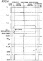
- a logic gate such as an AND gate, is usually provided to block any detection signal of the opening error detecting circuit with an output of the activated thermal shutdown circuit such that a detection signal Err_OP of the opening error detecting circuit is not output (not output at a detectable level) during the output TSD of the thermal shutdown circuit (high-level period) (indicated by area A defined by a dash-dot line in Fig. 6 ), as illustrated in Fig. 6 .
- a regulator IC including a short-circuiting error detecting circuit is further provided with an opening error detecting circuit and a thermal shutdown circuit
- external terminals that output signals of the circuits are usually provided to inform an external unit of the activation of the circuits.
- this increases the number of external terminals and thereby the size of the chip.
- JP 2016 103140 A discloses an IC.
- An object of the present invention which has been conceived in light of the issues described above, is to provide a semiconductor integrated circuit (regulator IC) of a DC power supply, such as a series regulator, including an error detecting circuit that detects an opened state of an output terminal, another error detecting circuit that detects a short-circuiting state, and a thermal shutdown circuit, the regulator IC outputting the operational states of the circuits to an external unit through a small number of external terminals, thereby preventing an increase in chip size.
- a semiconductor integrated circuit (regulator IC) of a DC power supply, such as a series regulator, including an error detecting circuit that detects an opened state of an output terminal, another error detecting circuit that detects a short-circuiting state, and a thermal shutdown circuit, the regulator IC outputting the operational states of the circuits to an external unit through a small number of external terminals, thereby preventing an increase in chip size.
- Another object of the present invention is to provide a semiconductor integrated circuit (regulator IC) that can detect errors such as an opening or short-circuiting of a load connected to the output terminal without a sense resistor and select the current value for detection of errors, such as an opening or short-circuiting, of a load connected to the output terminal depending on the system to which the regulator IC is to be applied.
- regulator IC semiconductor integrated circuit
- a semiconductor integrated circuit for a regulator including:
- the semiconductor integrated circuit for a regulator having the configuration described above detects the opened and short-circuiting states of the output terminals and outputs detection signals to an external unit, to reduce the load on the controller (CPU), such as a microcomputer controlling the system.
- the controller such as a microcomputer controlling the system.
- the semiconductor integrated circuit for a regulator outputs a signal indicating the logic sum of the output of the thermal shutdown circuit and the output of the short-circuiting error detecting circuit from the second output terminal as a short-circuiting error detection signal.
- the semiconductor integrated circuit for a regulator has a smaller number of external terminals compared to the number of external terminals needed for separately outputting signals from the terminal shutdown circuit and the short-circuiting error detecting circuit.
- the semiconductor integrated circuit for a regulator includes the first output terminal for outputting the result detected by the opening error detecting circuit to an external unit and is configured such that the output of the opening error detecting circuit is not blocked based on the output of the thermal shutdown circuit.
- the controller such as a microcomputer (CPU) can determine whether a short-circuiting error detection signal rose due to an overcurrent that does not activate the thermal shutdown circuit or full short-circuiting.
- the semiconductor integrated circuit for a regulator includes:
- opening and short-circuiting errors of a load connected to an output terminal is detected on the basis of a current proportional to the current flowing in the voltage control transistor, i.e., detected without a sense resistor for detecting the output current.
- opening errors can be more accurately detected than a configuration including a sense resistor having a low resistance connected to the input terminal.
- the semiconductor integrated circuit for a regulator includes:
- the semiconductor integrated circuit for a regulator includes:
- the current value to be the reference of an opening error and the current value to be the reference of a short-circuiting error can be arbitrarily and highly accurately determined in accordance with the system.
- the semiconductor integrated circuit (regulator IC) of a DC power supply such as a series regulator, according to the present invention includes an error detecting circuit that detects an opened state of an output terminal, another error detecting circuit that detects a short-circuiting state, and a thermal shutdown circuit.
- a regulator IC can output the operational states of the circuits to external unit(s) through a small number of external terminals, thereby preventing an increase in chip size.
- the regulator IC can detect errors such as an opening or short-circuiting of a load connected to the output terminal without a sense resistor and select the current value for detection of errors, such as an opening or short-circuiting, of a load connected to the output terminal in accordance with the system to which the regulator IC is to be applied.
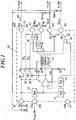
- Fig. 1 illustrates a series regulator or DC power supply according to an embodiment of the present invention.
- the area defined by a dash-dot line indicates a semiconductor integrated circuit (regulator IC) 10 disposed on a semiconductor chip, such as a monocrystalline silicon chip.
- the regulator IC 10 has an output terminal OUT connected to a capacitor Co and functions as a DC power supply that supplies a stable DC voltage.
- a voltage control transistor Q1 consisting of PNP bipolar transistor is connected to both the voltage input terminal IN to which a DC voltage Vin is applied and the output terminal OUT, and bleeder resistors R1 and R2 that divide the output voltage Vout and are connected in series to both the output terminal OUT and the ground line to which the ground voltage GND is applied.
- the voltage VFB divided by the bleeder resistors R1 and R2 is fed back to a non-inverting input terminal of an error amplifier 11 or error amplifier circuit that controls the base terminal of the voltage control transistor Q1.
- the error amplifier 11 controls the voltage control transistor Q1 in response to a potential difference between the outputted feedback voltage VFB and a reference voltage Vref, to produce a predetermined potential for the output voltage Vout.
- the regulator IC 10 includes a reference voltage circuit 12 that generates the reference voltage Vref to be applied to the inverting input terminal of the error amplifier 11; a bias circuit 13 that feeds an operational current to the error amplifier 11, the reference voltage circuit 12, and other components; a current limiting circuit 14 that is connected to the base terminal of the voltage control transistor Q1 to limit the output current; and a thermal shutdown circuit 15 that stops the operation of the error amplifier 11 and turns off the voltage control transistor Q1 if the temperature of the chip reaches a predetermined value.
- the reference voltage circuit 12 includes, for example, a resistor and a Zener diode disposed in series.
- the bias circuit 13 supplies or blocks a bias current to the error amplifier 11 in response to the control signal Cont from a microcomputer (CPU) being an external unit outside the chip to an external terminal CNT.
- the current limiting circuit 14 limits the output current through clamping of a base current higher than a predetermined value when an increased output current due to, for example, an abnormal load decreases the output voltage, and, in response, the error amplifier 11 decreases the base voltage to increase the current flowing to the transistor Q1.
- the regulator IC 10 includes bipolar transistors Q2, Q3, and Q4 disposed in parallel with the voltage control transistor Q1.
- the bipolar transistors Q2, Q3, and Q4 and the voltage control transistor Q1 define a current mirror circuit.
- a voltage identical to that applied to the base terminal of the voltage control transistor Q1 is applied to the base terminals or control terminals of the transistor Q2 to Q4.
- This causes a current (1/N) proportional to the collector current of the transistor Q1 to flow in the transistors Q2 to Q4 in accordance with the size ratio N of the device.
- the transistor Q1 includes N transistors having the same dimensions disposed in parallel with and the transistors Q2 to Q4 each include a single transistor, a current is controlled to be proportional to the number of devices.
- the regulator IC 10 includes an external terminal P1 that is connected to a resistor Rop for current-to-voltage conversion at an external unit outside the chip and an external terminal P2 that is connected to a resistor Rsc.
- the collector terminal of the current mirror transistor Q2 is connected to the external terminal P1, and the collector terminal of the current mirror transistor Q3 is connected to the external terminal P2.
- the regulator IC 10 further includes a comparator 16 for detecting an opening error having an inverting input terminal connected to the external terminal P1 and a non-inverting input terminal receiving a reference voltage Vref'; and a comparator 17 for detecting a short-circuiting error having a non-inverting input terminal connected to the external terminal P2 and an inverting input terminal receiving the reference voltage Vref'.
- the resistance of the external resistor Rop is determined such that the voltage across the terminals of the resistor is identical to the reference voltage Vref' while a detection current for an opening error of, for example, 10 mA flows in the voltage control transistor Q1.
- the resistance of the external resistor Rsc is determined such that the voltage across the terminals of the resistor is identical to the reference voltage Vref' while a detection current for a short-circuiting error of, for example, 200 mA flows in the voltage control transistor Q1.
- the external resistors Rop and Rsc determine the current values for the detection of an opening error and a short-circuiting error.
- the detection current (thresholds) can have any value in accordance with the system to be used, and the same reference voltage Vref' can be used for both the comparators 16 and 17, to simplify the circuit generating the reference voltage.
- the regulator IC 10 includes an NPN transistor Q5 having a base terminal connected to the output terminal of the comparator 16, an OR gate 18 that receives the output of the comparator 17 and the output of the thermal shutdown circuit 15, and an NPN transistor Q6 having a base terminal connected to the output terminal of the OR gate 18.
- the regulator IC chip includes external terminals P3 and P4 for an open-collector output of signals to an external unit, such as a CPU.
- the collector terminal of the transistor Q5 is connected to the external terminal P3, and the collector terminal of the transistor Q6 is connected to the external terminal P4.
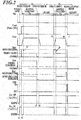
- the period T1 on the left half indicates a certain time of routine operation after activation of the regulator and the timing of an opening after the routine operation
- the period T2 on the right half indicates a certain time of routine operation after activation of the regulator and the timing of short-circuiting after the routine operation.
- the regulator IC 10 upon rising of an input voltage Vin at a timing t1 and then rising of a signal Cont of the control terminal CNT from an external unit to a high level at a timing t2, the regulator IC 10 is activated, and the output voltage Vout rises and is controlled to a predetermined voltage. A rush current flows toward the capacitor Co connected to the output terminal during the transitional period until the output voltage Vout rises, and then a steady current in accordance with the load status flows (period Ta).
- the output current Iout suddenly decreases (timing t3).
- the current flowing in the current mirror transistor Q2 also decreases in a similar manner.
- the comparator 16 detects this decrease, and its output increases to a high level.
- the transistor Q5 turns on, and the signal Err-OP from the external terminal P3 decreases to a low level.
- the CPU receiving this signal can detect an opening error.
- the CPU decreases the control signal Cont to a low level, to stop the operation of the regulator IC 10 (timing t4).
- the elimination of the opening error state causes the control signal Cont to increase to a high level at a timing t5.
- the regulator IC 10 resumes operation and controls the output voltage Vout to rise to a predetermined voltage. Also at this time, a rush current flows during a transitional period until the output voltage Vout rises, and then a steady current in accordance with the load status flows (period Tb).
- the output current Iout suddenly increases (timing t6).
- the current flowing in the current mirror transistor Q3 also increases in a similar manner.
- the comparator 17 detects this increase, and its output increases to a high level.
- the transistor Q6 turns on, and the signal Err-SC from the external terminal P4 decreases to a low level.
- the CPU receiving this signal can detect a short-circuiting error.
- the output current Iout suddenly increases and generates a high electrical power as heat.
- the thermal shutdown circuit blocks the output Iout because the operation of the error amplifier 11 is stopped to turn off the transistor Q1 if the temperature of the chip reaches a predetermined temperature. As a result, the detection of the short-circuiting state is reset. A decrease in the temperature of the semiconductor chip due to radiation of heat cancels the shutdown. If the short-circuiting state continues, the short-circuiting state is detected and is output. Such operations are repeated, generating a faulty short-circuiting error detection signal.
- the regulator IC 10 includes the OR gate 18, which determines the logic sum of the output of the comparator 17 and the output of the thermal shutdown circuit 15.
- the output of the OR gate 18 turns on/off the transistor Q6. If a short-circuiting error occurs and the output current Iout suddenly increases, a short-circuiting error detection signal is output and causes an increase in the temperature of the chip.
- the transistor Q6 is turned on or off by the logic sum of the output of the comparator 17 and the output of the thermal shutdown circuit 15 to continue the short-circuiting error detection signal. In this way, the short-circuiting error detection signal of the regulator IC 10 can be prevented from being generated through such repeated operation described above.
- the control signal Cont decreases to a low level to stop the operation of the regulator IC 10 (timing t7).
- a rush current flows immediately after the regulator IC 10 is activated.
- the rush current increases the output of the comparator 17 to a high level to turn on the transistor Q6 and decreases the signal Err-SC to a low level.
- Such false detection of the signal can be corrected by the CPU, which receives the signal, through execution of a dead-band program for ignoring a pulsed signal for detection of short-circuiting immediately after power is turned on.
- the operation of the thermal shutdown circuit 15 turns off the voltage control transistor Q1 and the current mirror transistor Q2, and the output of the comparator 16 is inverted to output an opening error detection signal Err_OP.
- the external microcomputer (CPU) receiving the signal may erroneously detect an opening error.
- the IC illustrated in Fig. 1 includes a logic gate, such as an AND gate, that blocks the detection signal of the opening error detecting circuit (comparator 16) with the output of the activated thermal shutdown circuit 15; and an inverter that inverts the output of the thermal shutdown circuit 15.
- the IC having a configuration in which the output of the inverter is applied to one of the input terminals of the AND gate usually does not output a detection signal Err_OP of the opening error detecting circuit while the output TSD of the thermal shutdown circuit rises (high level period), as illustrated in Fig. 6 (refer to the area A defined by the dot-dash line in Fig. 6 ).
- the output of the thermal shutdown circuit 15 and the detection signal of the short-circuiting error detecting circuit (comparator 17) are usually output from separate external terminals.
- the detection signal Err_SC in Fig. 6 indicates the signal timing in such configuration.
- the regulator IC 10 outputs a signal Err_SC of the logic sum of the output of the thermal shutdown circuit 15 and the detection signal of the short-circuiting error detecting circuit (17), from the external terminal P4.
- the number of external terminals can be reduced in comparison with that in a regulator IC that separately generates the output of the thermal shutdown circuit 15 and the detection signal of the short-circuiting error detecting circuit (17).
- an overcurrent small enough not to activate the thermal shutdown circuit 15 flows, or a relatively large current flows due to short-circuiting of a load and causes an increase in the temperature of the chip, thereby activating the thermal shutdown circuit 15.
- the external microcomputer CPU cannot determine whether the detection signal Err_SC rose due to activation of the thermal shutdown circuit 15 or due to detection of an overcurrent that does not activate the thermal shutdown circuit 15 by the short-circuiting error detecting circuit (17).
- the external microcomputer (CPU) of the regulator IC outputs a detection signal Err_OP if the opening error detecting circuit (16) detects an opening error even during rising of the output TSD of the thermal shutdown circuit 15 (high level period), as illustrated in the timing chart of Fig. 2 .
- the external microcomputer (CPU) can determine whether the detection signal Err_SC rises due to an overcurrent that does not activate the thermal shutdown circuit 15 or due to full short-circuiting.
- full short-circuiting causes activation of the thermal shutdown circuit 15 always after rising of the short-circuiting error detection signal Err_SC, to vary the opening error detection signal Err_OP.
- the external microcomputer CPU
- the external microcomputer can distinguish between an accidental overcurrent and full short-circuiting through monitoring of the signal Err_SC of the external terminal P4 and the signal Err_OP of the external terminal P3.
- different processes can be carried out in response to detection of a predetermined overcurrent and detection of high heat due to operation of the thermal shutdown circuit, as indicated by the period between timings t6 and t7 in Fig. 2 .
- a false operation such as turning off the regulator due to misidentifying an accidental overcurrent as full short-circuiting, can be prevented.
- a regulator IC according to a modification of this embodiment will now be described with reference to Figs. 3 and 4 .
- Fig. 3 illustrates a regulator IC according to a first modification.
- the regulator IC 10 according to this modification includes a delay circuit 19 including a resistor and a capacitor that delay the outputs of the comparators 16 and 17, a NOR gate 20 that determines the logic sum of the outputs of the comparators 16 and 17 and outputs the logic sum to the delay circuit 19, and AND gates 21 and 22 that determine the logic product of the output of the delay circuit 19 and the outputs of the comparators 16 and 17 before delay.
- the regulator IC determines a short-circuiting state when a relatively large current flows toward the output terminals.
- a relatively large rush current flows toward the capacitor Co of the output terminal.
- the regulator IC illustrated in Fig. 1 cannot distinguish between such a rush current and a current that flows toward an output terminal during a short-circuiting error.
- a false detection pulse generated in response to detection of a rush current Ir inevitably interferes with the output of the comparator 17, as illustrated in the timing chart in Fig. 2 .
- the system including the regulator IC according to this modification does not generate a false detection signal even if a rush current is detected. In this way, a dead-band program is not required for the downstream CPU.
- the delay circuit 19 includes a constant current source IC0, a capacitor C1 charged by the constant current source IC0, a resistor R4 and a switch transistor Qs connected in series to both the connection node N1 of the constant current source ICO and the capacitor C1 and a ground point, and a comparator CMP.
- the base terminal of the transistor Qs receives an output voltage of the NOR gate 20.
- the delay circuit 19 further includes an external terminal P5 connected to the connection node N1.
- the external terminal P5 is connected to an external capacitor Cd to increase the delay time without an increased chip size.
- the base terminal of the transistor Qs is turned on by a high-level output of the NOR gate 20, and the capacitors C1 and Cd are in a discharge state. If an opened state of the comparator 16 or a short-circuiting state of the comparator 17 is detected and the output of one of the comparators increases to a high-level, the output of the NOR gate 20 decreases to a low level to turn off the transistor Qs.
- the capacitors C1 and Cd are gradually charged, and the potential of the connection node N1 gradually increases.
- the output of the comparator CMP varies from a low level to a high level.
- the output of the AND gate 21 increases to a high level to turn on the transistor Q5, and the output of the external terminal P3 varies from the high level to a low level.
- the output of the AND gate 22 increases to a high level to turn on the transistor Q6, and the output of the external terminal P4 varies from a high level to a low level.
- the delay time of the delay circuit 19 is controlled to be slightly longer than the period during which the rush current Ir illustrated in Fig. 2 flows.
- the delay circuit 19, the comparator CMP, and the AND gates 21 and 22 according to this modification prevent the generation of a false detection pulse in response to detection of a rush current.
- Fig. 3 illustrates a configuration in which the delay circuit 19 delays the outputs of the comparators 16 and 17.
- the delay circuit 19 delays the outputs of the comparators 16 and 17.
- only the output of the comparator 17 for detecting a short-circuiting error may be delayed.
- the NOR gate 20 and the AND gate 21 in Fig. 3 are omitted.
- Fig. 4 illustrates a regulator IC according to a second modification.
- the comparator 17 for detecting a short-circuiting error according to the embodiment illustrated in Fig. 1 also functions as a comparator of the current limiting circuit 14.
- the current mirror transistor Q3 that feeds a monitoring current for detecting a short-circuiting error can also function as the current mirror transistor Q4 generating a monitoring current of the current limiting circuit 14.
- the current mirror transistor Q4 and the external terminal P2 in Fig. 1 are omitted, and an internal resistor R4 that converts the current of the current mirror transistor Q3 to a voltage is provided.
- the voltage converted by the internal resistor R4 is inputted to a non-inverting input terminal of the comparator 17 for detecting a short-circuiting error.
- the output of the comparator 17 and the output of the thermal shutdown circuit 15 are inputted to the base terminal of the transistor Q6 for output via the OR gate 18.
- the output of the comparator 17 is applied to the base terminals of the voltage control transistor Q1 and the current mirror transistors Q2 and Q3 via inverters 23 and 24. If a current having a value larger than a predetermined current value flows in the voltage control transistor Q1, the voltage control transistor Q1 is clamped to limit the output current Iout.
- the regulator IC according to the second modification has one less external terminal compared with the external terminals in the regulator IC according to the embodiment illustrated in Fig. 1 , and the short-circuiting error detecting circuit can function as a current limiting circuit.
- the chip can have reduced dimensions.
- the comparator 17 for detecting a short-circuiting error can function as the comparator of the current limiting circuit 14 while the external terminal P2 may be provided to connect an external resistor R4 for adjustment of the detection current (threshold).
- the voltage control transistor Q1 and the current mirror transistors Q2 to Q4 are bipolar transistors. Besides bipolar transistors, MOSFETs may also be used.
- the bleeder resistors R1 and R2 that divide the output voltages are disposed inside the chip.
- a dividing circuit including an external resistor may be provided to feed the voltage divided outside the chip from an external terminal to the error amplifier 11.
- a DC power supply including the series regulator according to the embodiments described above may be effectively used for in-vehicle electronic devices, such as car navigation systems, ETC systems, audio systems, and antennas. Besides such in-vehicle electronic devices, the DC power supply including the series regulator according to the embodiments described above may also be used in any system having loads activated by DC power.
Landscapes
- Engineering & Computer Science (AREA)
- Power Engineering (AREA)
- Physics & Mathematics (AREA)
- Electromagnetism (AREA)
- General Physics & Mathematics (AREA)
- Radar, Positioning & Navigation (AREA)
- Automation & Control Theory (AREA)
- Continuous-Control Power Sources That Use Transistors (AREA)
- Protection Of Static Devices (AREA)
Claims (4)
- Integrierte Halbleiterschaltung (10) für einen Regler, mit:einem Spannungssteuertransistor (Q1), der sowohl mit einem Spannungseingangsanschluss (IN), der eine Gleichspannung empfängt, als auch mit einem Spannungsausgangsanschluss (OUT) verbunden ist;einer Steuerschaltung (11), die den Spannungssteuertransistor (Q1) in Abhängigkeit einer Rückkopplungsspannung eines Ausgangs steuert;einer Offen-Fehler-Detektierschaltung (16), die einen offenen Zustand des Spannungsausgangsanschlusses (OUT) detektiert;einer Kurzschlussfehler-Detektierschaltung (17), die einen Kurzschlusszustand des Spannungsausgangsanschlusses (OUT) detektiert;einem ersten Ausgangsanschluss (P3), der ein von der Offen-Fehler-Detektierschaltung (16) detektiertes Ergebnis an eine externe Einheit ausgibt;einem zweiten Ausgangsanschluss (P4), der ein von der Kurzschlussfehler-Detektierschaltung (17) detektiertes Ergebnis an die externe Einheit ausgibt; undeiner Schaltung für thermisches Abschalten (15), die die Temperatur eines Halbleitersubstrats einschließlich der darauf angeordneten integrierten Halbleiterschaltung (10) detektiert und es der Steuerschaltung (11) ermöglicht, den Spannungssteuertransistor (Q1) auszuschalten, wenn die detektierte Temperatur des Halbleitersubstrats eine vorbestimmte Temperatur übersteigt,dadurch gekennzeichnet, dassein Signal, das die logische Summe eines Ausgangssignals der Schaltung für thermisches Abschalten (15) und eines Ausgangssignals der Kurzschlussfehler-Detektierschaltung (17) kennzeichnet, aus dem zweiten Ausgangsanschluss (P4) ausgegeben wird, sodass das Ausgangssignal der Offen-Fehler-Detektierschaltung (16) auf der Grundlage des Ausgangssignals der Schaltung für thermisches Abschalten (15) nicht blockiert wird.
- Integrierte Halbleiterschaltung (10) für einen Regler nach Anspruch 1, mit:einem ersten Transistor (Q2) und einem zweiten Transistor (Q3), die parallel zu dem Spannungssteuertransistor (Q1) angeordnet sind, wobei ein Strom, der anteilsmäßig zu einem Strom, der in dem Spannungssteuertransistor (Q1) fließt, abwärtsskaliert ist, in dem ersten Transistor (Q2) und dem zweiten Transistor (Q3) fließt, wobeidie Offen-Fehler-Detektierschaltung (16) eine erste Spannungsvergleichsschaltung, die die aus dem in dem ersten Transistor (Q2) fließenden Strom umgewandelte Spannung in der Größe mit einer vorbestimmten Vergleichsspannung vergleicht,die Kurzschlussfehler-Detektierschaltung (17) eine zweite Spannungsvergleichsschaltung aufweist, die die aus dem in dem zweiten Transistor (Q3) fließenden Strom umgewandelte Spannung in der Größe mit einer vorbestimmten Vergleichsspannung vergleicht, undwenn ein Strom mit einem Wert, der kleiner ist als der Wert eines vorbestimmten Offen-Fehler-Detektiersstroms, in dem ersten Transistor (Q2) fließt, das Ausgangssignal der ersten Spannungsvergleichsschaltung invertiert wird, und wenn ein Strom mit einem Wert, der größer ist als der Wert eines vorbestimmten Kurzschlussfehler-Detektierstroms, in dem zweiten Transistor (Q3) fließt, das Ausgangssignal der zweiten Spannungsvergleichsschaltung invertiert wird.
- Integrierte Halbleiterschaltung (10) für einen Regler nach Anspruch 2, mit:einer Verzögerungsschaltung (19), die von der ersten Spannungsvergleichsschaltung und der zweiten Spannungsvergleichsschaltung zumindest die Ausgabe der zweiten Spannungsvergleichsschaltung verzögert,wobei ein Signal, das das logische Produkt des Ausgangssignals der zweiten Spannungsvergleichsschaltung und des Signals, das von der Verzögerungsschaltung verzögert wird, keinzeichnet, aus dem zweiten Ausgangsanschluss (P4) als ein Kurzschlussfehler-Detektiersignal ausgegeben wird.
- Integrierte Halbleiterschaltung (10) für einen Regler nach Anspruch 2 oder 3, mit:einem ersten externen Anschluss (P1), der mit einem ersten Strom-Spannungs-Wandler (Rop) zum Umwandeln des in dem ersten Transistor (Q2) fließenden Stroms in eine Spannung verbunden ist; undeinem zweiten externen Anschluss (P2), der mit einem zweiten Strom-Spannungs-Wandler (Rsc) zur Umwandlung des in dem zweiten Transistor (Q3) fließenden Stroms in eine Spannung verbunden ist, wobeidie erste Spannungsvergleichsschaltung die von dem mit dem ersten externen Anschluss (P1) verbundenen ersten Strom-Spannungs-Wandler (Rop) umgewandelte Spannung mit einer vorbestimmten Vergleichsspannung vergleicht, unddie zweite Spannungsvergleichsschaltung die von dem mit dem zweiten externen Anschluss (P2) verbundenen Strom-Spannungs-Wandler (Rsc) umgewandelte Spannung mit einer vorbestimmten Vergleichsspannung vergleicht.
Applications Claiming Priority (1)
| Application Number | Priority Date | Filing Date | Title |
|---|---|---|---|
| JP2016193092A JP6784918B2 (ja) | 2016-09-30 | 2016-09-30 | レギュレータ用半導体集積回路 |
Publications (2)
| Publication Number | Publication Date |
|---|---|
| EP3301537A1 EP3301537A1 (de) | 2018-04-04 |
| EP3301537B1 true EP3301537B1 (de) | 2019-03-27 |
Family
ID=60009451
Family Applications (1)
| Application Number | Title | Priority Date | Filing Date |
|---|---|---|---|
| EP17193612.3A Active EP3301537B1 (de) | 2016-09-30 | 2017-09-28 | Integrierte halbleiterschaltung für regler |
Country Status (4)
| Country | Link |
|---|---|
| US (1) | US10063135B2 (de) |
| EP (1) | EP3301537B1 (de) |
| JP (1) | JP6784918B2 (de) |
| CN (1) | CN107885270B (de) |
Families Citing this family (10)
| Publication number | Priority date | Publication date | Assignee | Title |
|---|---|---|---|---|
| US10831222B2 (en) | 2018-04-03 | 2020-11-10 | Mitsumi Electric Co., Ltd. | Semiconductor apparatus for power supply control and output voltage variable power supply apparatus |
| JP7106966B2 (ja) * | 2018-04-27 | 2022-07-27 | 市光工業株式会社 | 車両用灯具 |
| CN108922487B (zh) * | 2018-08-24 | 2020-06-26 | 惠科股份有限公司 | 电压调节电路及显示装置 |
| JP7010205B2 (ja) * | 2018-12-25 | 2022-01-26 | 横河電機株式会社 | 2線式伝送器 |
| JP7265140B2 (ja) | 2019-05-20 | 2023-04-26 | ミツミ電機株式会社 | 電源制御用半導体装置および出力電圧可変電源装置並びに設計方法 |
| JP2021022281A (ja) * | 2019-07-30 | 2021-02-18 | ミツミ電機株式会社 | 電源制御用半導体装置および出力電圧可変電源装置 |
| JP7352086B2 (ja) * | 2019-12-18 | 2023-09-28 | ミツミ電機株式会社 | レギュレータ用半導体集積回路およびファンモータシステム |
| JP2022044133A (ja) | 2020-09-07 | 2022-03-17 | ミツミ電機株式会社 | 電源用半導体集積回路 |
| JP2022044215A (ja) | 2020-09-07 | 2022-03-17 | ミツミ電機株式会社 | 電源用半導体集積回路 |
| US11782087B2 (en) | 2021-08-05 | 2023-10-10 | Mitsumi Electric Co., Ltd. | Semiconductor integrated circuit |
Family Cites Families (25)
| Publication number | Priority date | Publication date | Assignee | Title |
|---|---|---|---|---|
| US6392472B1 (en) * | 1999-06-18 | 2002-05-21 | Mitsubishi Denki Kabushiki Kaisha | Constant internal voltage generation circuit |
| US6522111B2 (en) * | 2001-01-26 | 2003-02-18 | Linfinity Microelectronics | Linear voltage regulator using adaptive biasing |
| JP2003152513A (ja) * | 2001-11-08 | 2003-05-23 | Nf Corp | 半導体素子の温度バランス回路 |
| US7924542B2 (en) * | 2005-06-03 | 2011-04-12 | Autonetworks Technologies, Ltd. | Power supply controller and semiconductor device |
| JP4666316B2 (ja) * | 2008-01-15 | 2011-04-06 | ▲ぎょく▼瀚科技股▲ふん▼有限公司 | 電流感知回路ループのある定電流調整器 |
| JP2009169785A (ja) * | 2008-01-18 | 2009-07-30 | Seiko Instruments Inc | ボルテージレギュレータ |
| JP5099505B2 (ja) * | 2008-02-15 | 2012-12-19 | セイコーインスツル株式会社 | ボルテージレギュレータ |
| JP5347669B2 (ja) * | 2009-04-10 | 2013-11-20 | ミツミ電機株式会社 | レギュレータ |
| JP5491223B2 (ja) * | 2009-06-17 | 2014-05-14 | セイコーインスツル株式会社 | 過熱保護回路及び電源用集積回路 |
| JP2012093296A (ja) | 2010-10-28 | 2012-05-17 | Clarion Co Ltd | 電源回路、車載ナビゲーション装置 |
| JP2013012000A (ja) * | 2011-06-29 | 2013-01-17 | Mitsumi Electric Co Ltd | レギュレータ用半導体集積回路 |
| JP2013021117A (ja) * | 2011-07-11 | 2013-01-31 | Rohm Co Ltd | Led駆動装置、照明装置、液晶表示装置 |
| JP2013102603A (ja) | 2011-11-08 | 2013-05-23 | Rohm Co Ltd | 半導体装置およびこれを用いたスイッチングレギュレータ |
| JP5939675B2 (ja) * | 2012-04-20 | 2016-06-22 | ルネサスエレクトロニクス株式会社 | 半導体装置及び制御システム |
| US10041982B2 (en) * | 2012-08-15 | 2018-08-07 | Texas Instruments Incorporated | Switch mode power converter current sensing apparatus and method |
| EP2713492B1 (de) * | 2012-09-26 | 2019-11-27 | ams AG | Leistungsumwandlungsanordnung und Verfahren zur Leistungsumwandlung |
| US9088211B2 (en) * | 2013-02-14 | 2015-07-21 | Texas Instruments Incorporated | Buck-boost converter with buck-boost transition switching control |
| JP6180815B2 (ja) | 2013-06-21 | 2017-08-16 | エスアイアイ・セミコンダクタ株式会社 | ボルテージレギュレータ |
| JP6371543B2 (ja) * | 2014-03-14 | 2018-08-08 | エイブリック株式会社 | 過熱保護回路及びボルテージレギュレータ |
| US9780648B2 (en) * | 2014-08-30 | 2017-10-03 | Ixys Corporation | Synchronous sensing of inductor current in a buck converter control circuit |
| EP3010131B1 (de) * | 2014-10-15 | 2019-09-04 | Dialog Semiconductor (UK) Ltd | Gleichstromabwärtswandler mit Taktimpulsfrequenzmodulation |
| JP6405948B2 (ja) * | 2014-11-28 | 2018-10-17 | ミツミ電機株式会社 | レギュレータ用半導体集積回路 |
| DE102015204518B4 (de) * | 2015-03-12 | 2017-04-13 | Dialog Semiconductor (Uk) Limited | Offset-Kompensation für einen VDS-Ausgleicher in einer Stromerfassungsschaltung |
| JP6500588B2 (ja) * | 2015-05-15 | 2019-04-17 | ミツミ電機株式会社 | レギュレータ用半導体集積回路 |
| US9793800B1 (en) * | 2016-04-15 | 2017-10-17 | Linear Technology Corporation | Multiphase switching power supply with robust current sensing and shared amplifier |
-
2016
- 2016-09-30 JP JP2016193092A patent/JP6784918B2/ja active Active
-
2017
- 2017-09-27 CN CN201710892694.8A patent/CN107885270B/zh active Active
- 2017-09-28 EP EP17193612.3A patent/EP3301537B1/de active Active
- 2017-09-29 US US15/721,364 patent/US10063135B2/en active Active
Non-Patent Citations (1)
| Title |
|---|
| None * |
Also Published As
| Publication number | Publication date |
|---|---|
| JP6784918B2 (ja) | 2020-11-18 |
| CN107885270A (zh) | 2018-04-06 |
| JP2018055545A (ja) | 2018-04-05 |
| EP3301537A1 (de) | 2018-04-04 |
| US10063135B2 (en) | 2018-08-28 |
| US20180097439A1 (en) | 2018-04-05 |
| CN107885270B (zh) | 2020-07-03 |
Similar Documents
| Publication | Publication Date | Title |
|---|---|---|
| EP3301537B1 (de) | Integrierte halbleiterschaltung für regler | |
| JP6663103B2 (ja) | レギュレータ用半導体集積回路 | |
| TWI398747B (zh) | 功率級控制電路 | |
| US20080224680A1 (en) | Voltage regulator | |
| US11474549B2 (en) | Semiconductor integrated circuit for regulator, and fan motor system | |
| US7724552B2 (en) | Power supply | |
| US11768510B2 (en) | Power supply semiconductor integrated circuit including a short-circuit-fault detection circuit that detects a short circuit of the voltage-output terminal | |
| US20070210834A1 (en) | Reset detection circuit in semiconductor integrated circuit | |
| CN110069093B (zh) | 电源控制装置 | |
| US20220182049A1 (en) | Semiconductor integrated circuit device | |
| US10128738B2 (en) | Determination of entering and exiting safe mode | |
| JP2022044133A (ja) | 電源用半導体集積回路 | |
| US9343959B2 (en) | Interrupt protection circuits, systems and methods for sensors and other devices | |
| JP2011082785A (ja) | パワーオンリセット回路 | |
| US20130241508A1 (en) | Voltage regulator | |
| JP7352512B2 (ja) | 電源回路及び電子制御装置 | |
| US11824524B2 (en) | Semiconductor device | |
| JP7257164B2 (ja) | クランプ回路 | |
| JP2000353020A (ja) | レギュレータ回路 | |
| JP2023023298A (ja) | 電源用半導体集積回路および電源用レギュレータ回路 | |
| KR20000044338A (ko) | 전원공급장치의 출력 과전압 보호회로 | |
| JP2019062657A (ja) | 電源供給装置 | |
| JP2018128762A (ja) | リニアレギュレータ、その保護方法、それを用いたdc/dcコンバータの制御回路、車載電装機器 | |
| JP2021536017A (ja) | 電圧検出システム |
Legal Events
| Date | Code | Title | Description |
|---|---|---|---|
| PUAI | Public reference made under article 153(3) epc to a published international application that has entered the european phase |
Free format text: ORIGINAL CODE: 0009012 |
|
| STAA | Information on the status of an ep patent application or granted ep patent |
Free format text: STATUS: THE APPLICATION HAS BEEN PUBLISHED |
|
| AK | Designated contracting states |
Kind code of ref document: A1 Designated state(s): AL AT BE BG CH CY CZ DE DK EE ES FI FR GB GR HR HU IE IS IT LI LT LU LV MC MK MT NL NO PL PT RO RS SE SI SK SM TR |
|
| AX | Request for extension of the european patent |
Extension state: BA ME |
|
| STAA | Information on the status of an ep patent application or granted ep patent |
Free format text: STATUS: REQUEST FOR EXAMINATION WAS MADE |
|
| REG | Reference to a national code |
Ref country code: DE Ref legal event code: R079 Ref document number: 602017002948 Country of ref document: DE Free format text: PREVIOUS MAIN CLASS: G05F0001560000 Ipc: H02M0003156000 |
|
| 17P | Request for examination filed |
Effective date: 20180903 |
|
| RBV | Designated contracting states (corrected) |
Designated state(s): AL AT BE BG CH CY CZ DE DK EE ES FI FR GB GR HR HU IE IS IT LI LT LU LV MC MK MT NL NO PL PT RO RS SE SI SK SM TR |
|
| GRAP | Despatch of communication of intention to grant a patent |
Free format text: ORIGINAL CODE: EPIDOSNIGR1 |
|
| STAA | Information on the status of an ep patent application or granted ep patent |
Free format text: STATUS: GRANT OF PATENT IS INTENDED |
|
| RIC1 | Information provided on ipc code assigned before grant |
Ipc: H02M 3/158 20060101ALI20180927BHEP Ipc: H02M 3/156 20060101AFI20180927BHEP Ipc: H02M 1/32 20070101ALI20180927BHEP Ipc: H03K 17/08 20060101ALI20180927BHEP Ipc: G05F 1/56 20060101ALI20180927BHEP |
|
| INTG | Intention to grant announced |
Effective date: 20181019 |
|
| GRAS | Grant fee paid |
Free format text: ORIGINAL CODE: EPIDOSNIGR3 |
|
| GRAA | (expected) grant |
Free format text: ORIGINAL CODE: 0009210 |
|
| STAA | Information on the status of an ep patent application or granted ep patent |
Free format text: STATUS: THE PATENT HAS BEEN GRANTED |
|
| AK | Designated contracting states |
Kind code of ref document: B1 Designated state(s): AL AT BE BG CH CY CZ DE DK EE ES FI FR GB GR HR HU IE IS IT LI LT LU LV MC MK MT NL NO PL PT RO RS SE SI SK SM TR |
|
| REG | Reference to a national code |
Ref country code: GB Ref legal event code: FG4D |
|
| REG | Reference to a national code |
Ref country code: CH Ref legal event code: EP |
|
| REG | Reference to a national code |
Ref country code: AT Ref legal event code: REF Ref document number: 1114213 Country of ref document: AT Kind code of ref document: T Effective date: 20190415 |
|
| REG | Reference to a national code |
Ref country code: IE Ref legal event code: FG4D |
|
| REG | Reference to a national code |
Ref country code: DE Ref legal event code: R096 Ref document number: 602017002948 Country of ref document: DE |
|
| PG25 | Lapsed in a contracting state [announced via postgrant information from national office to epo] |
Ref country code: SE Free format text: LAPSE BECAUSE OF FAILURE TO SUBMIT A TRANSLATION OF THE DESCRIPTION OR TO PAY THE FEE WITHIN THE PRESCRIBED TIME-LIMIT Effective date: 20190327 Ref country code: NO Free format text: LAPSE BECAUSE OF FAILURE TO SUBMIT A TRANSLATION OF THE DESCRIPTION OR TO PAY THE FEE WITHIN THE PRESCRIBED TIME-LIMIT Effective date: 20190627 Ref country code: LT Free format text: LAPSE BECAUSE OF FAILURE TO SUBMIT A TRANSLATION OF THE DESCRIPTION OR TO PAY THE FEE WITHIN THE PRESCRIBED TIME-LIMIT Effective date: 20190327 Ref country code: FI Free format text: LAPSE BECAUSE OF FAILURE TO SUBMIT A TRANSLATION OF THE DESCRIPTION OR TO PAY THE FEE WITHIN THE PRESCRIBED TIME-LIMIT Effective date: 20190327 |
|
| REG | Reference to a national code |
Ref country code: NL Ref legal event code: MP Effective date: 20190327 |
|
| PG25 | Lapsed in a contracting state [announced via postgrant information from national office to epo] |
Ref country code: GR Free format text: LAPSE BECAUSE OF FAILURE TO SUBMIT A TRANSLATION OF THE DESCRIPTION OR TO PAY THE FEE WITHIN THE PRESCRIBED TIME-LIMIT Effective date: 20190628 Ref country code: BG Free format text: LAPSE BECAUSE OF FAILURE TO SUBMIT A TRANSLATION OF THE DESCRIPTION OR TO PAY THE FEE WITHIN THE PRESCRIBED TIME-LIMIT Effective date: 20190627 Ref country code: RS Free format text: LAPSE BECAUSE OF FAILURE TO SUBMIT A TRANSLATION OF THE DESCRIPTION OR TO PAY THE FEE WITHIN THE PRESCRIBED TIME-LIMIT Effective date: 20190327 Ref country code: LV Free format text: LAPSE BECAUSE OF FAILURE TO SUBMIT A TRANSLATION OF THE DESCRIPTION OR TO PAY THE FEE WITHIN THE PRESCRIBED TIME-LIMIT Effective date: 20190327 Ref country code: NL Free format text: LAPSE BECAUSE OF FAILURE TO SUBMIT A TRANSLATION OF THE DESCRIPTION OR TO PAY THE FEE WITHIN THE PRESCRIBED TIME-LIMIT Effective date: 20190327 Ref country code: HR Free format text: LAPSE BECAUSE OF FAILURE TO SUBMIT A TRANSLATION OF THE DESCRIPTION OR TO PAY THE FEE WITHIN THE PRESCRIBED TIME-LIMIT Effective date: 20190327 |
|
| REG | Reference to a national code |
Ref country code: AT Ref legal event code: MK05 Ref document number: 1114213 Country of ref document: AT Kind code of ref document: T Effective date: 20190327 |
|
| PG25 | Lapsed in a contracting state [announced via postgrant information from national office to epo] |
Ref country code: CZ Free format text: LAPSE BECAUSE OF FAILURE TO SUBMIT A TRANSLATION OF THE DESCRIPTION OR TO PAY THE FEE WITHIN THE PRESCRIBED TIME-LIMIT Effective date: 20190327 Ref country code: RO Free format text: LAPSE BECAUSE OF FAILURE TO SUBMIT A TRANSLATION OF THE DESCRIPTION OR TO PAY THE FEE WITHIN THE PRESCRIBED TIME-LIMIT Effective date: 20190327 Ref country code: ES Free format text: LAPSE BECAUSE OF FAILURE TO SUBMIT A TRANSLATION OF THE DESCRIPTION OR TO PAY THE FEE WITHIN THE PRESCRIBED TIME-LIMIT Effective date: 20190327 Ref country code: AL Free format text: LAPSE BECAUSE OF FAILURE TO SUBMIT A TRANSLATION OF THE DESCRIPTION OR TO PAY THE FEE WITHIN THE PRESCRIBED TIME-LIMIT Effective date: 20190327 Ref country code: PT Free format text: LAPSE BECAUSE OF FAILURE TO SUBMIT A TRANSLATION OF THE DESCRIPTION OR TO PAY THE FEE WITHIN THE PRESCRIBED TIME-LIMIT Effective date: 20190727 Ref country code: SK Free format text: LAPSE BECAUSE OF FAILURE TO SUBMIT A TRANSLATION OF THE DESCRIPTION OR TO PAY THE FEE WITHIN THE PRESCRIBED TIME-LIMIT Effective date: 20190327 Ref country code: IT Free format text: LAPSE BECAUSE OF FAILURE TO SUBMIT A TRANSLATION OF THE DESCRIPTION OR TO PAY THE FEE WITHIN THE PRESCRIBED TIME-LIMIT Effective date: 20190327 Ref country code: EE Free format text: LAPSE BECAUSE OF FAILURE TO SUBMIT A TRANSLATION OF THE DESCRIPTION OR TO PAY THE FEE WITHIN THE PRESCRIBED TIME-LIMIT Effective date: 20190327 |
|
| PG25 | Lapsed in a contracting state [announced via postgrant information from national office to epo] |
Ref country code: SM Free format text: LAPSE BECAUSE OF FAILURE TO SUBMIT A TRANSLATION OF THE DESCRIPTION OR TO PAY THE FEE WITHIN THE PRESCRIBED TIME-LIMIT Effective date: 20190327 Ref country code: PL Free format text: LAPSE BECAUSE OF FAILURE TO SUBMIT A TRANSLATION OF THE DESCRIPTION OR TO PAY THE FEE WITHIN THE PRESCRIBED TIME-LIMIT Effective date: 20190327 |
|
| PG25 | Lapsed in a contracting state [announced via postgrant information from national office to epo] |
Ref country code: IS Free format text: LAPSE BECAUSE OF FAILURE TO SUBMIT A TRANSLATION OF THE DESCRIPTION OR TO PAY THE FEE WITHIN THE PRESCRIBED TIME-LIMIT Effective date: 20190727 Ref country code: AT Free format text: LAPSE BECAUSE OF FAILURE TO SUBMIT A TRANSLATION OF THE DESCRIPTION OR TO PAY THE FEE WITHIN THE PRESCRIBED TIME-LIMIT Effective date: 20190327 |
|
| REG | Reference to a national code |
Ref country code: DE Ref legal event code: R097 Ref document number: 602017002948 Country of ref document: DE |
|
| PG25 | Lapsed in a contracting state [announced via postgrant information from national office to epo] |
Ref country code: DK Free format text: LAPSE BECAUSE OF FAILURE TO SUBMIT A TRANSLATION OF THE DESCRIPTION OR TO PAY THE FEE WITHIN THE PRESCRIBED TIME-LIMIT Effective date: 20190327 |
|
| PLBE | No opposition filed within time limit |
Free format text: ORIGINAL CODE: 0009261 |
|
| STAA | Information on the status of an ep patent application or granted ep patent |
Free format text: STATUS: NO OPPOSITION FILED WITHIN TIME LIMIT |
|
| PG25 | Lapsed in a contracting state [announced via postgrant information from national office to epo] |
Ref country code: SI Free format text: LAPSE BECAUSE OF FAILURE TO SUBMIT A TRANSLATION OF THE DESCRIPTION OR TO PAY THE FEE WITHIN THE PRESCRIBED TIME-LIMIT Effective date: 20190327 |
|
| 26N | No opposition filed |
Effective date: 20200103 |
|
| PG25 | Lapsed in a contracting state [announced via postgrant information from national office to epo] |
Ref country code: TR Free format text: LAPSE BECAUSE OF FAILURE TO SUBMIT A TRANSLATION OF THE DESCRIPTION OR TO PAY THE FEE WITHIN THE PRESCRIBED TIME-LIMIT Effective date: 20190327 |
|
| PG25 | Lapsed in a contracting state [announced via postgrant information from national office to epo] |
Ref country code: MC Free format text: LAPSE BECAUSE OF FAILURE TO SUBMIT A TRANSLATION OF THE DESCRIPTION OR TO PAY THE FEE WITHIN THE PRESCRIBED TIME-LIMIT Effective date: 20190327 |
|
| PG25 | Lapsed in a contracting state [announced via postgrant information from national office to epo] |
Ref country code: IE Free format text: LAPSE BECAUSE OF NON-PAYMENT OF DUE FEES Effective date: 20190928 Ref country code: LU Free format text: LAPSE BECAUSE OF NON-PAYMENT OF DUE FEES Effective date: 20190928 |
|
| REG | Reference to a national code |
Ref country code: BE Ref legal event code: MM Effective date: 20190930 |
|
| PG25 | Lapsed in a contracting state [announced via postgrant information from national office to epo] |
Ref country code: BE Free format text: LAPSE BECAUSE OF NON-PAYMENT OF DUE FEES Effective date: 20190930 |
|
| PG25 | Lapsed in a contracting state [announced via postgrant information from national office to epo] |
Ref country code: FR Free format text: LAPSE BECAUSE OF NON-PAYMENT OF DUE FEES Effective date: 20190930 |
|
| REG | Reference to a national code |
Ref country code: CH Ref legal event code: PL |
|
| PG25 | Lapsed in a contracting state [announced via postgrant information from national office to epo] |
Ref country code: CY Free format text: LAPSE BECAUSE OF FAILURE TO SUBMIT A TRANSLATION OF THE DESCRIPTION OR TO PAY THE FEE WITHIN THE PRESCRIBED TIME-LIMIT Effective date: 20190327 |
|
| PG25 | Lapsed in a contracting state [announced via postgrant information from national office to epo] |
Ref country code: MT Free format text: LAPSE BECAUSE OF FAILURE TO SUBMIT A TRANSLATION OF THE DESCRIPTION OR TO PAY THE FEE WITHIN THE PRESCRIBED TIME-LIMIT Effective date: 20190327 Ref country code: HU Free format text: LAPSE BECAUSE OF FAILURE TO SUBMIT A TRANSLATION OF THE DESCRIPTION OR TO PAY THE FEE WITHIN THE PRESCRIBED TIME-LIMIT; INVALID AB INITIO Effective date: 20170928 |
|
| PG25 | Lapsed in a contracting state [announced via postgrant information from national office to epo] |
Ref country code: CH Free format text: LAPSE BECAUSE OF NON-PAYMENT OF DUE FEES Effective date: 20200930 Ref country code: LI Free format text: LAPSE BECAUSE OF NON-PAYMENT OF DUE FEES Effective date: 20200930 |
|
| GBPC | Gb: european patent ceased through non-payment of renewal fee |
Effective date: 20210928 |
|
| PG25 | Lapsed in a contracting state [announced via postgrant information from national office to epo] |
Ref country code: MK Free format text: LAPSE BECAUSE OF FAILURE TO SUBMIT A TRANSLATION OF THE DESCRIPTION OR TO PAY THE FEE WITHIN THE PRESCRIBED TIME-LIMIT Effective date: 20190327 |
|
| PG25 | Lapsed in a contracting state [announced via postgrant information from national office to epo] |
Ref country code: GB Free format text: LAPSE BECAUSE OF NON-PAYMENT OF DUE FEES Effective date: 20210928 |
|
| PGFP | Annual fee paid to national office [announced via postgrant information from national office to epo] |
Ref country code: DE Payment date: 20230920 Year of fee payment: 7 |