EP3279366B1 - Cible de pulvérisation cathodique en alliage cu-ga et son procédé de fabrication - Google Patents
Cible de pulvérisation cathodique en alliage cu-ga et son procédé de fabrication Download PDFInfo
- Publication number
- EP3279366B1 EP3279366B1 EP16772177.8A EP16772177A EP3279366B1 EP 3279366 B1 EP3279366 B1 EP 3279366B1 EP 16772177 A EP16772177 A EP 16772177A EP 3279366 B1 EP3279366 B1 EP 3279366B1
- Authority
- EP
- European Patent Office
- Prior art keywords
- grain size
- sputtering target
- alloy sputtering
- alloy
- crystal grains
- Prior art date
- Legal status (The legal status is an assumption and is not a legal conclusion. Google has not performed a legal analysis and makes no representation as to the accuracy of the status listed.)
- Active
Links
- 229910000807 Ga alloy Inorganic materials 0.000 title claims description 137
- 238000005477 sputtering target Methods 0.000 title claims description 102
- 238000004519 manufacturing process Methods 0.000 title claims description 40
- 238000005245 sintering Methods 0.000 claims description 96
- 239000013078 crystal Substances 0.000 claims description 93
- 239000000843 powder Substances 0.000 claims description 81
- OKTJSMMVPCPJKN-UHFFFAOYSA-N Carbon Chemical compound [C] OKTJSMMVPCPJKN-UHFFFAOYSA-N 0.000 claims description 64
- 229910052799 carbon Inorganic materials 0.000 claims description 64
- 230000000052 comparative effect Effects 0.000 claims description 55
- 238000000034 method Methods 0.000 claims description 45
- 238000004544 sputter deposition Methods 0.000 claims description 42
- QVGXLLKOCUKJST-UHFFFAOYSA-N atomic oxygen Chemical compound [O] QVGXLLKOCUKJST-UHFFFAOYSA-N 0.000 claims description 18
- 229910052760 oxygen Inorganic materials 0.000 claims description 18
- 239000001301 oxygen Substances 0.000 claims description 18
- 239000007791 liquid phase Substances 0.000 claims description 9
- 238000005259 measurement Methods 0.000 claims description 6
- 238000010521 absorption reaction Methods 0.000 claims description 4
- 239000007769 metal material Substances 0.000 claims description 4
- GRYLNZFGIOXLOG-UHFFFAOYSA-N Nitric acid Chemical compound O[N+]([O-])=O GRYLNZFGIOXLOG-UHFFFAOYSA-N 0.000 claims description 3
- 229910017604 nitric acid Inorganic materials 0.000 claims description 3
- 230000003287 optical effect Effects 0.000 claims description 3
- 238000001000 micrograph Methods 0.000 claims description 2
- 238000005452 bending Methods 0.000 description 32
- 230000002159 abnormal effect Effects 0.000 description 25
- 230000015572 biosynthetic process Effects 0.000 description 24
- 239000010408 film Substances 0.000 description 24
- 239000002245 particle Substances 0.000 description 23
- 239000011148 porous material Substances 0.000 description 12
- 238000002490 spark plasma sintering Methods 0.000 description 10
- 239000010949 copper Substances 0.000 description 9
- 239000010409 thin film Substances 0.000 description 9
- 238000011156 evaluation Methods 0.000 description 7
- 239000000203 mixture Substances 0.000 description 7
- 238000005266 casting Methods 0.000 description 6
- 230000008018 melting Effects 0.000 description 6
- 238000002844 melting Methods 0.000 description 6
- 230000000694 effects Effects 0.000 description 5
- 229910002059 quaternary alloy Inorganic materials 0.000 description 5
- 238000003754 machining Methods 0.000 description 4
- 229910052802 copper Inorganic materials 0.000 description 3
- 230000007423 decrease Effects 0.000 description 3
- 239000006185 dispersion Substances 0.000 description 3
- 238000009826 distribution Methods 0.000 description 3
- 238000011049 filling Methods 0.000 description 3
- 238000010438 heat treatment Methods 0.000 description 3
- 238000001513 hot isostatic pressing Methods 0.000 description 3
- 238000007731 hot pressing Methods 0.000 description 3
- 238000002347 injection Methods 0.000 description 3
- 239000007924 injection Substances 0.000 description 3
- 239000000463 material Substances 0.000 description 3
- 238000003825 pressing Methods 0.000 description 3
- 239000002994 raw material Substances 0.000 description 3
- RYGMFSIKBFXOCR-UHFFFAOYSA-N Copper Chemical compound [Cu] RYGMFSIKBFXOCR-UHFFFAOYSA-N 0.000 description 2
- 229910045601 alloy Inorganic materials 0.000 description 2
- 239000000956 alloy Substances 0.000 description 2
- 238000013213 extrapolation Methods 0.000 description 2
- 239000007789 gas Substances 0.000 description 2
- 239000012535 impurity Substances 0.000 description 2
- 238000013519 translation Methods 0.000 description 2
- 238000007740 vapor deposition Methods 0.000 description 2
- 238000006243 chemical reaction Methods 0.000 description 1
- 150000001875 compounds Chemical class 0.000 description 1
- 239000004020 conductor Substances 0.000 description 1
- 230000001186 cumulative effect Effects 0.000 description 1
- 238000000151 deposition Methods 0.000 description 1
- 230000008021 deposition Effects 0.000 description 1
- 238000002474 experimental method Methods 0.000 description 1
- 238000009689 gas atomisation Methods 0.000 description 1
- 238000007373 indentation Methods 0.000 description 1
- 239000007788 liquid Substances 0.000 description 1
- 238000001755 magnetron sputter deposition Methods 0.000 description 1
- 238000010587 phase diagram Methods 0.000 description 1
- 238000002360 preparation method Methods 0.000 description 1
- 238000005204 segregation Methods 0.000 description 1
- 239000004065 semiconductor Substances 0.000 description 1
- 238000007711 solidification Methods 0.000 description 1
- 230000008023 solidification Effects 0.000 description 1
- 239000000243 solution Substances 0.000 description 1
- 239000000758 substrate Substances 0.000 description 1
- 238000011179 visual inspection Methods 0.000 description 1
Images


Classifications
-
- B—PERFORMING OPERATIONS; TRANSPORTING
- B22—CASTING; POWDER METALLURGY
- B22F—WORKING METALLIC POWDER; MANUFACTURE OF ARTICLES FROM METALLIC POWDER; MAKING METALLIC POWDER; APPARATUS OR DEVICES SPECIALLY ADAPTED FOR METALLIC POWDER
- B22F3/00—Manufacture of workpieces or articles from metallic powder characterised by the manner of compacting or sintering; Apparatus specially adapted therefor ; Presses and furnaces
- B22F3/10—Sintering only
- B22F3/105—Sintering only by using electric current other than for infrared radiant energy, laser radiation or plasma ; by ultrasonic bonding
-
- B—PERFORMING OPERATIONS; TRANSPORTING
- B22—CASTING; POWDER METALLURGY
- B22F—WORKING METALLIC POWDER; MANUFACTURE OF ARTICLES FROM METALLIC POWDER; MAKING METALLIC POWDER; APPARATUS OR DEVICES SPECIALLY ADAPTED FOR METALLIC POWDER
- B22F3/00—Manufacture of workpieces or articles from metallic powder characterised by the manner of compacting or sintering; Apparatus specially adapted therefor ; Presses and furnaces
- B22F3/12—Both compacting and sintering
- B22F3/14—Both compacting and sintering simultaneously
-
- C—CHEMISTRY; METALLURGY
- C22—METALLURGY; FERROUS OR NON-FERROUS ALLOYS; TREATMENT OF ALLOYS OR NON-FERROUS METALS
- C22C—ALLOYS
- C22C9/00—Alloys based on copper
-
- C—CHEMISTRY; METALLURGY
- C23—COATING METALLIC MATERIAL; COATING MATERIAL WITH METALLIC MATERIAL; CHEMICAL SURFACE TREATMENT; DIFFUSION TREATMENT OF METALLIC MATERIAL; COATING BY VACUUM EVAPORATION, BY SPUTTERING, BY ION IMPLANTATION OR BY CHEMICAL VAPOUR DEPOSITION, IN GENERAL; INHIBITING CORROSION OF METALLIC MATERIAL OR INCRUSTATION IN GENERAL
- C23C—COATING METALLIC MATERIAL; COATING MATERIAL WITH METALLIC MATERIAL; SURFACE TREATMENT OF METALLIC MATERIAL BY DIFFUSION INTO THE SURFACE, BY CHEMICAL CONVERSION OR SUBSTITUTION; COATING BY VACUUM EVAPORATION, BY SPUTTERING, BY ION IMPLANTATION OR BY CHEMICAL VAPOUR DEPOSITION, IN GENERAL
- C23C14/00—Coating by vacuum evaporation, by sputtering or by ion implantation of the coating forming material
- C23C14/22—Coating by vacuum evaporation, by sputtering or by ion implantation of the coating forming material characterised by the process of coating
- C23C14/34—Sputtering
- C23C14/3407—Cathode assembly for sputtering apparatus, e.g. Target
- C23C14/3414—Metallurgical or chemical aspects of target preparation, e.g. casting, powder metallurgy
-
- H—ELECTRICITY
- H01—ELECTRIC ELEMENTS
- H01L—SEMICONDUCTOR DEVICES NOT COVERED BY CLASS H10
- H01L31/00—Semiconductor devices sensitive to infrared radiation, light, electromagnetic radiation of shorter wavelength or corpuscular radiation and specially adapted either for the conversion of the energy of such radiation into electrical energy or for the control of electrical energy by such radiation; Processes or apparatus specially adapted for the manufacture or treatment thereof or of parts thereof; Details thereof
- H01L31/0248—Semiconductor devices sensitive to infrared radiation, light, electromagnetic radiation of shorter wavelength or corpuscular radiation and specially adapted either for the conversion of the energy of such radiation into electrical energy or for the control of electrical energy by such radiation; Processes or apparatus specially adapted for the manufacture or treatment thereof or of parts thereof; Details thereof characterised by their semiconductor bodies
- H01L31/0256—Semiconductor devices sensitive to infrared radiation, light, electromagnetic radiation of shorter wavelength or corpuscular radiation and specially adapted either for the conversion of the energy of such radiation into electrical energy or for the control of electrical energy by such radiation; Processes or apparatus specially adapted for the manufacture or treatment thereof or of parts thereof; Details thereof characterised by their semiconductor bodies characterised by the material
- H01L31/0264—Inorganic materials
- H01L31/032—Inorganic materials including, apart from doping materials or other impurities, only compounds not provided for in groups H01L31/0272 - H01L31/0312
- H01L31/0322—Inorganic materials including, apart from doping materials or other impurities, only compounds not provided for in groups H01L31/0272 - H01L31/0312 comprising only AIBIIICVI chalcopyrite compounds, e.g. Cu In Se2, Cu Ga Se2, Cu In Ga Se2
-
- B—PERFORMING OPERATIONS; TRANSPORTING
- B22—CASTING; POWDER METALLURGY
- B22F—WORKING METALLIC POWDER; MANUFACTURE OF ARTICLES FROM METALLIC POWDER; MAKING METALLIC POWDER; APPARATUS OR DEVICES SPECIALLY ADAPTED FOR METALLIC POWDER
- B22F1/00—Metallic powder; Treatment of metallic powder, e.g. to facilitate working or to improve properties
- B22F1/05—Metallic powder characterised by the size or surface area of the particles
- B22F1/052—Metallic powder characterised by the size or surface area of the particles characterised by a mixture of particles of different sizes or by the particle size distribution
-
- Y—GENERAL TAGGING OF NEW TECHNOLOGICAL DEVELOPMENTS; GENERAL TAGGING OF CROSS-SECTIONAL TECHNOLOGIES SPANNING OVER SEVERAL SECTIONS OF THE IPC; TECHNICAL SUBJECTS COVERED BY FORMER USPC CROSS-REFERENCE ART COLLECTIONS [XRACs] AND DIGESTS
- Y02—TECHNOLOGIES OR APPLICATIONS FOR MITIGATION OR ADAPTATION AGAINST CLIMATE CHANGE
- Y02E—REDUCTION OF GREENHOUSE GAS [GHG] EMISSIONS, RELATED TO ENERGY GENERATION, TRANSMISSION OR DISTRIBUTION
- Y02E10/00—Energy generation through renewable energy sources
- Y02E10/50—Photovoltaic [PV] energy
- Y02E10/541—CuInSe2 material PV cells
Definitions
- the present invention relates to a Cu-Ga alloy sputtering target used for forming a Cu-Ga alloy film by sputtering, and a method of manufacturing the Cu-Ga alloy sputtering target.
- a CIGS solar cell that includes a light-absorbing layer formed of a Cu-In-Ga-Se quaternary alloy thin film is widely provided.
- a solar cell that includes a light-absorbing layer formed using a vapor deposition method has an advantageous effect in that the energy conversion efficiency is high, but has a problem in that the deposition rate is slow and the production efficiency is low.
- a method of forming the light-absorbing layer formed of a Cu-In-Ga-Se quaternary alloy thin film a method of forming a laminated film including an In film and a Cu-Ga film and performing a heat treatment on the laminated film in a Se atmosphere to selenize the laminated film, is provided.
- a sputtering method in which an In sputtering target and a Cu-Ga alloy sputtering target are used is applied.
- the Cu-Ga alloy sputtering target is manufactured using a melting/casting method (for example, PTLs 1 and 2) or a powder-sintering method (for example, PTLs 3, 4 and 5).
- a melting/casting method for example, PTLs 1 and 2
- a powder-sintering method for example, PTLs 3, 4 and 5
- a Cu-Ga alloy sputtering target manufactured using a melting/casting method has an advantageous effect in that the oxygen concentration is low and the sputtering rate is fast, but has a problem in that segregation of Ga occurs during solidification and crystal grains are coarsened.
- a Cu-Ga alloy sputtering target manufactured using a powder-sintering method has an advantageous effect in that the bending strength is high and the target is not likely to break during sputtering due to its fine structure, but has a problem in that the oxygen concentration is high and the sputtering rate is slow.
- the Cu-Ga alloy sputtering target manufactured using a powder-sintering method has a problem in that the brittleness is high and breaking is likely to occur.
- the amount of impurities is larger than that in the Cu-Ga alloy sputtering target manufactured using a melting/casting method. Therefore, during sputtering film formation, abnormal discharge may occur, particles may be formed, and the quality of a formed Cu-Ga alloy film may deteriorate.
- the present invention has been made in consideration of the above-described circumstances, and an object thereof is to provide: a Cu-Ga alloy sputtering target in which breaking can be suppressed during manufacturing or use and in which abnormal discharge and particle formation can be suppressed during sputtering film formation; and a method of manufacturing the Cu-Ga alloy sputtering target.
- a Cu-Ga alloy sputtering target made of a Cu-Ga alloy in which a carbon concentration is 1.0 ppm by mass to 30 ppm by mass, an oxygen concentration is 150 ppm by mass or lower, and, in an observed structure, an area ratio of crystal grains having a grain size of 10 ⁇ m or less is 5% to 50% and an area ratio of crystal grains having a grain size of 100 ⁇ m or more is 1% to 30%.
- an area ratio of crystal grains having a grain size of 10 ⁇ m or less is 5% or higher and an area ratio of crystal grains having a grain size of 100 ⁇ m or more is 1 % or higher. Therefore, the number of pores present in crystal grains can be reduced, and the bending strength can be improved. As a result, breaking can be suppressed during manufacturing or use.
- the carbon concentration is limited to 1.0 ppm by mass to 30 ppm by mass and the area ratio of crystal grains having a grain size of 10 ⁇ m or less is limited to 50% or lower. Therefore, particle formation can be suppressed during sputtering film formation, and a high-quality Cu-Ga alloy film can be formed.
- the area ratio of crystal grains having a grain size of 100 ⁇ m or more is limited to 30% or lower. Therefore, abnormal discharge during sputtering film formation can be suppressed. That is, the sputtering rate varies depending on crystal orientations. Therefore, as sputtering progresses, unevenness is formed on the sputtering surface due to the variation in sputtering rate. In a case where a large amount of crystal grains having a grain size of 100 ⁇ m or more are present, unevenness formed on the sputtering surface becomes significant, electric charges are concentrated on convex portions, and abnormal discharge is likely to occur. Therefore, by limiting the area ratio of the crystal grains having a grain size of 100 ⁇ m or more to 30% or lower, abnormal discharge can be suppressed.
- an average crystal grain size be 100 ⁇ m or less.
- an oxygen concentration is 150 ppm by mass or lower.
- a method of manufacturing a Cu-Ga alloy sputtering target is provided, the Cu-Ga alloy sputtering target being the above-described Cu-Ga alloy sputtering target.
- This method includes a sintering step of sintering base powder, in which a carbon concentration in the base powder is 1.0 ppm by mass to 140 ppm by mass a proportion of grains having a grain size of 10 ⁇ m or less in the base powder is 5% to 50% by volume, a proportion of grains having a grain size of 100 ⁇ m or more in the base powder is 1% to 30% by volume, and the base powder is sintered using a pulsed electric-current pressure sintering method in the sintering step, at an applied pressure of 1 MPa to 100 MPa, a sintering temperature T s in a range of 0.5xT L ⁇ T S ⁇ T L with respect to a liquid phase appearance temperature T S of a Cu-Ga alloy constituting a Cu-Ga
- the base powder is sintered using a pulsed electric-current pressure sintering method (also known as a spark plasma sintering method (SPS)). Therefore, the grain size of the base powder becomes the crystal grain size of the Cu-Ga alloy sputtering target without a significant change in the grain size of the base powder. Accordingly, in the base powder-preparing step, the proportion of grains having a grain size of 10 ⁇ m or less contained in the base powder is adjusted to be 5% to 50% by volume, and the proportion of grains having a grain size of 100 ⁇ m or more is adjusted to be 1% to 30% by volume.
- a pulsed electric-current pressure sintering method also known as a spark plasma sintering method (SPS)
- a Cu-Ga alloy sputtering target can be manufactured in which the area ratio of crystal grains having a grain size of 10 ⁇ m or less is limited to 5% to 50% and the area ratio of crystal grains having a grain size of 100 ⁇ m or more is 1% to 30%.
- the base powder is sintered using a pulsed electric-current pressure sintering method.
- a pulsed electric-current pressure sintering method When an electric current passes through point contact portions between grains of the base powder, the cross-sectional area of an electric-current path significantly decreases, and the current density significantly increases. Therefore, the amount of Joule heat generated significantly increases, the temperature of a local region reaches a high temperature at which plasma is generated such that carbon is removed from the region, and thus the amount of carbon can be reduced during sintering. Accordingly, by adjusting the amount of carbon in the base powder to be 1.0 ppm by mass to 140 ppm by mass a Cu-Ga alloy sputtering target in which the carbon concentration is 1.0 ppm by mass to ppm by mass can be manufactured.
- a sintering temperature T S is in a range of 0.5 ⁇ T L ⁇ T S ⁇ T L with respect to a liquid phase appearance temperature T L of a Cu-Ga alloy constituting a Cu-Ga alloy sputtering target to be manufactured, and a holding time is 0.5 min to 60 min.
- the sintering temperature T S and the holding time are in the above-described ranges. Therefore, the base powder can reliably be sintered, and the melting of the base powder can be suppressed.
- the liquid phase appearance temperature T L represents a liquidus line or the lower limit of a solid-liquid coexisting region in a phase diagram.
- an applied pressure is 1 MPa to 100 MPa.
- the applied pressure is 1 MPa or higher in the sintering step. Therefore, an electric current can reliably be passed through the base powder to heat the base powder. In addition, the applied pressure is 100 MPa or lower in the sintering step. Therefore, it is not necessary to use large pressing facilities, a Cu-Ga alloy sputtering target can be efficiently manufactured.
- an average grain size of the base powder be 100 ⁇ m or less.
- the base powder is sintered using a pulsed electric-current pressure sintering method. Therefore, a Cu-Ga alloy sputtering target can be manufactured in which the average crystal grain size is 100 ⁇ m or less without a significant change in the grain size of the base powder.
- a mold including a cylindrical die and punches which are configured to be inserted into openings formed at opposite ends of the die, and a pressure be applied to the punches using a press machine while passing an electric current through the punches, and it is preferable that an auxiliary current-carrying member be disposed between the press machine and an end surface of the die in the vicinity of the punches.
- a Cu-Ga alloy sputtering target in which breaking can be suppressed during manufacturing or use and in which abnormal discharge and particle formation can be suppressed during sputtering film formation; and a method of manufacturing the Cu-Ga alloy sputtering target.
- the Cu-Ga alloy sputtering target according to the present embodiment is used when a Cu-Ga alloy film is formed by sputtering in order to form, for example, a light-absorbing layer formed of a Cu-In-Ga-Se quaternary alloy thin film in a CIGS thin-film solar cell.
- the Cu-Ga alloy sputtering target according to the present embodiment is made of a Cu-Ga alloy with a composition containing 20 at % to 40 at% of Ga and the balance being Cu and inevitable impurities.
- a carbon concentration is 30 ppm by mass or lower
- an oxygen concentration is 150 ppm by mass or lower.
- an area ratio of crystal grains having a grain size (crystal grain size) of 10 ⁇ m or less is 5% to 50% and an area ratio of crystal grains having a grain size of 100 ⁇ m or more is 1% to 30%. Further, an average crystal grain size therein is 100 ⁇ m or less.
- a Weibull modulus of bending strengths measured at five or more positions is 20 or more.
- a relative density is 99% or higher.
- a value is obtained by, in a graph in which the vertical axis represents a density and the horizontal axis represents a Ga composition ratio (Ga content), connecting a density ⁇ Cu of pure copper of 8.96 g/cm 3 and a density ⁇ CuGa of the Cu-Ga alloy (Cu: 69.23 at%, Ga: 30.77 at%) of 8.47 g/cm 3 through a straight line and performing interpolation or extrapolation according to the composition of the Cu-Ga alloy (Ga content). Then, the relative density according to the present embodiment is calculated by assuming that the obtained value is 100%.
- the method of manufacturing a Cu-Ga alloy sputtering target includes: a base powder-preparing step S01 of preparing base powder; a base powder-filling step S02 of filling a cavity formed in a mold with the base powder; a sintering step S03 of heating the base powder to a sintering temperature T S (°C) in a vacuum atmosphere to sinter it; and a machining step S04 of machining the obtained sintered body.
- Cu-Ga alloy powder as the base powder is prepared.
- the Cu-Ga alloy powder may be purchased or may be manufactured using, for example, the following atomizing method.
- a massive Cu raw material and a massive Ga raw material are weighed to obtain a predetermined composition and are put into a crucible made of carbon, and this crucible is set in a gas atomization device. After vacuum evacuation, the raw materials are melted by being held at a temperature of 1000°C to 1200°C for 1 minute to 30 minutes. Next, while causing the molten alloy to drop through nozzles having a pore size of 1 mm to 3 mm, Ar gas is injected at a gas injection pressure of 10 kgf/cm 2 to 50 kgf/cm 2 . As a result, gas-atomized powder is prepared. The obtained gas-atomized powder is cooled and then classified through a sieve.
- the molten alloy may reach a chamber before being solidified into powder.
- the injection temperature be set to be lower than a heating and holding temperature by about 100°C to 400°C.
- an average grain size (average particle size) is 100 ⁇ m or less.
- a proportion of grains having a grain size (particle size) of 10 ⁇ m or less is 5% to 50% by volume, and a proportion of grains having a grain size of 100 ⁇ m or more is 1 % to 30% by volume.
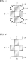
- a mold 10 to be filled with the base powder is prepared.
- a lower punch 12 is inserted into a lower side of a die 11 having a cylindrical shape. Thereby, a cavity is formed in the mold 10.
- an upper punch 13 is inserted.
- the mold 10 (the die 11, the lower punch 12, and the upper punch 13) is made of a conductive material such as carbon.
- the die 11 is not necessarily conductive.
- the filled base powder is heated to the sintering temperature T S (°C) and held to be sintered.
- the base powder is pressed with the upper punch 13 and the lower punch 12 using a press machine 20 which also functions as an electrode.
- an applied pressure be 1 MPa to 100 MPa.
- the sintering is performed in a vacuum atmosphere (pressure: 1000 Pa or lower).
- the sintering is performed using a pulsed electric-current pressure sintering method (also known as a spark plasma sintering method) in which an electric current is passed through the base powder to heat the base powder using Joule heat by applying electric power to the upper punch 13 and the lower punch 12 in the vacuum atmosphere.
- a conductive coil spring 15 as an auxiliary current-carrying member is provided in the vicinity of the lower punch 12 and the upper punch 13 (between an end surface of the press machine 20 and an end surface of the die 11).
- the press machine 20 and the die 11 are electrically connected through the coil spring 15.
- a current-carrying area increased by the coil spring 15 is 0.1 times or more of a current-carrying area of the die.
- the coil spring 15 shrinks between the press machine 20 and the end surface of the die 11, and the press machine 20 and the die 11 are electrically connected through the coil spring 15.
- the sintering temperature T S (°C) in the sintering step S03 is set to be in a range of 0.5 ⁇ T L ⁇ T S ⁇ T L with respect to a liquid phase appearance temperature T L of a Cu-Ga alloy constituting a Cu-Ga alloy sputtering target to be manufactured.
- a holding time at the sintering temperature T S (°C) is set to be in a range of 0.5 min to 60 min.
- a temperature increase rate is set to be in a range of 5 °C/min to 75 °C/min.
- a Cu-Ga alloy sputtering target having a predetermined size is manufactured.
- an area ratio of crystal grains having a grain size of 10 ⁇ m or less is 5% or higher and an area ratio of crystal grains having a grain size of 100 ⁇ m or more is 1% or higher.
- Substantially no pores are present in fine crystal grains having a grain size of 10 ⁇ m or less.
- the number of pores in coarse crystal grains having a grain size of 100 ⁇ m or more does not substantially increase although the grain size increases. Therefore, the number of pores per reference area decreases. Accordingly, an area ratio of crystal grains having a grain size of 10 ⁇ m or less is 5% or higher and an area ratio of crystal grains having a grain size of 100 ⁇ m or more is 1% or higher, whereby the number of pores in the crystal grains can be reduced.
- the bending strength decreases due to the presence of pores on crystal grain boundaries. Therefore, by reducing the number of pores in crystal grains to increase a ratio of the number of pores in crystal grains to the number of pores on crystal grain boundaries (the number of pores in crystal grains/the number of pores on crystal grain boundaries), the bending strength of the Cu-Ga alloy sputtering target can be improved. Thereby, breaking can be suppressed during manufacturing or use.
- the lower limit of the area ratio of crystal grains having a grain size of 10 ⁇ m or less be 10%.
- the lower limit of the area ratio of crystal grains having a grain size of 100 ⁇ m or more be 5%.
- the carbon concentration is limited to 30 ppm by mass or lower, the area ratio of crystal grains having a grain size of 10 ⁇ m or less is limited to 50% or lower, and the area ratio of crystal grains having a grain size of 100 ⁇ m or more is 1% or more. Therefore, particle formation can be suppressed during sputtering film formation.
- the present invention is not limited to this configuration.
- the upper limit of the area ratio of crystal grains having a grain size of 10 ⁇ m or less be 40%.
- the lower limit of the area ratio of crystal grains having a grain size of 100 ⁇ m or more be 5%.
- the area ratio of coarse crystal grains having a grain size of 100 ⁇ m or more is limited to 30% or lower. Therefore, even in a case where a sputtering surface is consumed along with the progress of sputtering, no significant unevenness is formed on the sputtering surface, and thus abnormal discharge caused by concentration of electric charges on convex portions can be suppressed.
- the average crystal grain size of the sputtering surface is 100 ⁇ m or less. Therefore, even in a case where the sputtering surface is consumed, no significant unevenness is formed on the sputtering surface, and thus abnormal discharge can reliably be suppressed.
- the oxygen concentration is 150 ppm by mass or lower. Therefore, formation of an oxide in the Cu-Ga alloy sputtering target can be suppressed, and abnormal discharge and particle formation caused by the oxide can be suppressed.
- the upper limit of the area ratio of crystal grains having a grain size of 100 ⁇ m or more be 20%.
- the average crystal grain size of the sputtering surface is preferably 75 ⁇ m or less.
- the lower limit of the average crystal grain size is preferably 25 ⁇ m, but the present invention is not limited thereto.
- the oxygen concentration is preferably 100 ppm by mass or lower.
- the lower limit of the oxygen concentration is preferably 1.0 ppm by mass, but the present invention is not limited thereto.
- the bending strength is represented by Y (MPa) and the Ga content in the Cu-Ga alloy is represented by X (at%), a relationship of Y ⁇ -8 ⁇ X+490 is satisfied. Therefore, the bending strength Y is sufficiently higher than that in the related art, and breaking can be suppressed.
- the Weibull modulus of bending strengths measured at five or more positions is 20 or higher. Therefore, a dispersion in the bending strength of the Cu-Ga alloy sputtering target is small, and breaking can be sufficiently suppressed.
- the Weibull modulus is calculated using the following method.
- F a cumulative probability of fracture of measured samples
- Y the bending strength
- the Weibull modulus is a slope of measured lines plotted on a graph in which the vertical axis represents lnln((1-F) -1 ) and the horizontal axis represents ln(Y).
- the Weibull modulus is preferably 50 or lower and more preferably 30 to 50, but the present invention is not limited thereto.
- the sintering is performed using a pulsed electric-current pressure sintering method (also known as a spark plasma sintering method) in which by applying electric power to the upper punch 13 and the lower punch 12, an electric current is passed through the base powder to heat the base powder by Joule heat. Therefore, the grain size of the base powder becomes the crystal grain size of the Cu-Ga alloy sputtering target without a significant change in the grain size of the base powder.
- a pulsed electric-current pressure sintering method also known as a spark plasma sintering method
- the grain size distribution of the base powder is adjusted such that the proportion of grains having a grain size of 10 ⁇ m or less is 5% to 50% by volume and the proportion of grains having a grain size of 100 ⁇ m or more is 1% to 30% by volume. Therefore, a Cu-Ga alloy sputtering target can be manufactured in which the area ratio of crystal grains having a grain size of 10 ⁇ m or less is limited to 5% to 50% and the area ratio of crystal grains having a grain size of 100 ⁇ m or more is 1% to 30%.
- the proportion of grains having a grain size of 10 ⁇ m or less is preferably 10% to 40% by volume, and the proportion of grains having a grain size of 100 ⁇ m or more is preferably 2.0% to 20% by volume.
- the present invention is not limited to this configuration.
- the average grain size of the Cu-Ga alloy powder is 100 ⁇ m or less. Therefore, a Cu-Ga alloy sputtering target having an average crystal grain size of 100 ⁇ m or less can be manufactured.
- the average grain size of the base powder is preferably 10 ⁇ m or more and more preferably 25 ⁇ m to 75 ⁇ m, but the present invention is not limited thereto.
- the sintering is performed using the pulsed electric-current pressure sintering method (also known as a spark plasma sintering method). Therefore, the amount of carbon can be reduced in the sintering step S03. Accordingly, by setting the amount of carbon in the base powder (Cu-Ga alloy powder) to be 140 ppm by mass or lower in the base powder-preparing step S01, a Cu-Ga alloy sputtering target in which the carbon concentration is 30 ppm by mass or lower can be manufactured.
- the lower limit of the amount of carbon in the base powder is preferably 1.0 ppm by mass and more preferably 1.0 ppm by mass to 20 ppm by mass. However, the present invention is not limited to this configuration.
- the base powder is sintered using the spark plasma sintering method (SPS) in the vacuum atmosphere (pressure: 1000 Pa or lower). Therefore, the amount of carbon can reliably be reduced.
- SPS spark plasma sintering method
- the vacuum atmosphere in the sintering step S03 be 50 Pa or lower.
- the sintering temperature T S is 0.5 ⁇ T L or higher with respect to the liquid phase appearance temperature T L of a Cu-Ga alloy constituting a Cu-Ga alloy sputtering target to be manufactured, and the holding time is 0.5 min or longer. Therefore, the base powder (Cu-Ga alloy powder) can reliably be sintered.
- the sintering temperature T S is the liquid phase appearance temperature T L or lower, and the holding time is 60 min or shorter. Therefore, in the sintering step S03, the melting of the base powder (Cu-Ga alloy powder) can be suppressed.
- the lower limit of the sintering temperature T S is preferably 0.7T L .
- the lower limit of the holding time is preferably 10 min.
- the upper limit of the sintering temperature T S is preferably 0.95T L .
- the upper limit of the holding time is preferably 30 min.
- the temperature increase rate in the sintering step S03 is set to be 5 °C/min to 75 °C/min and more preferably 15 °C/min to 50 °C/min.
- the applied pressure by the upper punch 13 and the lower punch 12 is set to be 1 MPa or higher. Therefore, an electric current can reliably be passed through the base powder (Cu-Ga alloy powder), the base powder can be heated, and thus the base powder (Cu-Ga alloy powder) can be reliably sintered.
- the applied pressure by the upper punch 13 and the lower punch 12 is set to be 100 MPa or lower. Therefore, since it is not necessary to use large pressing facilities, a Cu-Ga alloy sputtering target can be efficiently manufactured.
- the lower limit of the applied pressure in the sintering step S03 is preferably 10 MPa.
- the upper limit of the applied pressure in the sintering step S03 is preferably 70 MPa.
- the coil spring 15 as the auxiliary current-carrying member is provided in the vicinity of the lower punch 12 and the upper punch 13.
- the press machine 20 and the die 11 are electrically connected through the coil spring 15. Therefore, a difference in the amount of Joule heat generated between a region where only the lower punch 12 and the upper punch 13 are provided and a region where the die 11 is provided can be suppressed from significantly increasing, and a difference in temperature therebetween can be suppressed to be small. Thereby, the local formation of a portion where sintering is insufficient can be suppressed, and the bending strength can be significantly improved. In addition, a dispersion in the bending strength can also be suppressed.
- the Cu-Ga alloy sputtering target is used when a Cu-Ga alloy thin film is formed by sputtering in order to form a light-absorbing layer made of a Cu-In-Ga-Se quaternary alloy thin film in a solar cell.
- the present invention is not limited to this configuration, and the Cu-Ga alloy sputtering target may be used for another application.
- the shape and size of the Cu-Ga alloy sputtering target are not particularly limited and, for example, may be a rectangular shape, a disk shape, or a cylindrical shape.
- the coil spring 15 as the auxiliary current-carrying member is provided in the vicinity of the upper punch 13 and the lower punch 12.
- the present invention is not limited to this configuration, and a leaf spring 115 may be provided as shown in FIG. 3 , or a pinch spring 215 may be provided as shown in FIG. 4 .
- a conductive wire 315 may be provided.
- the auxiliary current-carrying member is not necessarily provided.
- base powders (Cu-Ga alloy powders) having compositions and grain size distributions shown in Tables 1 and 2 were prepared.
- Each of the base powders filled a mold.
- the molds die, upper punch, and lower punch
- Sintering was performed using a spark plasma sintering method under conditions shown in Tables 3 and 4.
- the auxiliary current-carrying member was not used.
- the size of the obtained Cu-Ga alloy sputtering target (sintered body) was ⁇ 100 mm ⁇ 10 mmt.
- Comparative Example 10 the base powder shown in Table 2 was sintered by hot pressing to manufacture a Cu-Ga alloy sputtering target.
- Comparative Example 11 the base powder shown in Table 2 was used through a casting method to manufacture a Cu-Ga alloy sputtering target.
- Comparative Example 12 the base powder shown in Table 2 was sintered using a hot isostatic pressing (HIP) method to manufacture a Cu-Ga alloy sputtering target.
- HIP hot isostatic pressing
- Table 4 shows preparation conditions of Comparative Examples 10, 11, and 12.
- the relative density, the oxygen concentration, the carbon concentration, the average crystal grain size, the area ratio of crystal grains having a grain size of 10 ⁇ m or less, the area ratio of crystal grains having a grain size of 100 ⁇ m or more, the bending strength, the number of particles formed during sputtering film formation, and the number of times of abnormal discharge were evaluated as follows.
- the density was measured using the Archimedes' method. A value is obtained by connecting a density ⁇ Cu of pure copper of 8.96 g/cm 3 and a density ⁇ CuGa of the Cu-Ga alloy (Cu: 69.23 at%, Ga: 30.77 at%) of 8.47 g/cm 3 through a straight line and performing interpolation or extrapolation according to the composition of the Cu-Ga alloy (Ga content). Then, the relative density was calculated by assuming that the obtained value is 100%. The evaluation results are shown in Tables 5 and 6.
- the oxygen concentration was measured using an infrared absorption method described in "General Rules for Determination of Oxygen in Metallic Materials” of JIS Z 2613. The measurement results are shown in Tables 5 and 6.
- the carbon concentration was measured using an infrared absorption method described in "General Rules for Determination of Carbon in Metallic Materials” of JIS Z 2615. The measurement results are shown in Tables 5 and 6.
- a sputtering surface was polished, was etched with nitric acid, and then was observed with an optical microscope. The measurement magnification was 250 times, and the observed area was 7.5 mm 2 or more.
- the crystal grain sizes of crystal grains were measured by line segment method, and the average crystal grain size, the area ratio of crystal grains having a grain size of 10 ⁇ m or less, and the area ratio of crystal grains having a grain size of 100 ⁇ m or more were calculated.
- the area ratio was calculated by drawing a square lattice where the interval between the lines is comparative with 5 ⁇ m on a printed micrograph of the structure and counting the number of squares contained in each grain. The evaluation results are shown in Tables 5 and 6.
- the sintered body was divided into three portions in a thickness direction (direction in which the upper punch and the lower punch pressed), five specimens (3 mm ⁇ 4 mm ⁇ 35 mm) were collected from a center portion in the thickness direction, and a stress trajectory was measured at an indentation speed of 0.5 mm/min using Autograph AG-X (manufactured by Shimadzu Corporation). A maximum point stress of an elastic area was obtained, and the bending strength was evaluated based on the average value of the five specimens. The evaluation results are shown in Tables 5 and 6.
- a Cu-Ga alloy film having a thickness of 100 nm was formed on a substrate having a diameter of ⁇ 100 mm by direct current (DC) sputtering under conditions of input power: 3.3 W/cm 2 and 10 min.
- DC direct current
- the Ar flow rate was 30 sccm
- the pressure was 0.67 Pa.
- the number of particles having a diameter of 0.3 ⁇ m or more present in the formed Cu-Ga alloy film was measured using a particle counter. The evaluation results are shown in Tables 5 and 6.
- Comparative Example 1 in which the amount of carbon was 35 ppm by mass, a large number of particles were formed during sputtering film formation and abnormal discharge occurred.
- Comparative Example 2 in which the area ratio of crystal grains having a grain size of 100 ⁇ m or more was 0.5%
- Comparative Example 4 in which the area ratio of crystal grains having a grain size of 10 ⁇ m or less was 3% and the area ratio of crystal grains having a grain size of 100 ⁇ m or more was 0.5%
- Comparative Example 5 in which the area ratio of crystal grains having a grain size of 10 ⁇ m or less was 3%.
- Comparative Example 3 in which the area ratio of crystal grains having a grain size of 100 ⁇ m or more was 50%
- Comparative Example 6 in which the area ratio of crystal grains having a grain size of 10 ⁇ m or less was 3% and the area ratio of crystal grains having a grain size of 100 ⁇ m or more was 50%
- Comparative Example 9 in which the area ratio of crystal grains having a grain size of 10 ⁇ m or less was 60% and the area ratio of crystal grains having a grain size of 100 ⁇ m or more was 50%.
- Comparative Example 7 in which the area ratio of crystal grains having a grain size of 10 ⁇ m or less was 60% and the area ratio of crystal grains having a grain size of 100 ⁇ m or more was 0.5%
- Comparative Example 8 in which the area ratio of crystal grains having a grain size of 10 ⁇ m or less was 60% and the area ratio of crystal grains having a grain size of 100 ⁇ m or more was 10%
- Comparative Example 9 in which the area ratio of crystal grains having a grain size of 10 ⁇ m or less was 60% and the area ratio of crystal grains having a grain size of 100 ⁇ m or more was 50%.
- Comparative Example 11 In Comparative Example 11 in which the target was manufactured through a casting method, no crystal grains having a grain size of 10 ⁇ m or less were present, the average crystal grain size was extremely large, and abnormal discharge occurred.
- Comparative Example 12 in which the sintering was performed using a hot isostatic pressing (HIP) method, the amount of carbon was large, the area ratio of crystal grains having a grain size of 10 ⁇ m or less and the area ratio of crystal grains having a grain size of 100 ⁇ m or more were outside of the range of the present invention, the number of particles was large, and abnormal discharge occurred.
- HIP hot isostatic pressing
- Table 7 also shows a Ga concentration X (at%) and a lower limit value Y 0 of a bending strength Y shown in the following Expression (1) using the Ga concentration X.
- the bending strength was significantly improved as compared to a case where the auxiliary current-carrying member was not used.
- the Weibull modulus increased, and a dispersion in bending strength was suppressed.
- the bending strength calculated from Expression (1) increased.
- the Cu-Ga alloy sputtering target according to the present invention breaking can be suppressed during manufacturing or use, and abnormal discharge and particle formation can be suppressed during sputtering film formation. Therefore, the Cu-Ga alloy sputtering target according to the present invention is suitable as a sputtering target which is used for forming a light-absorbing layer in a CIGS thin-film solar cell or the like.
Landscapes
- Chemical & Material Sciences (AREA)
- Engineering & Computer Science (AREA)
- Mechanical Engineering (AREA)
- Materials Engineering (AREA)
- Metallurgy (AREA)
- Organic Chemistry (AREA)
- Manufacturing & Machinery (AREA)
- Physics & Mathematics (AREA)
- Chemical Kinetics & Catalysis (AREA)
- Inorganic Chemistry (AREA)
- Condensed Matter Physics & Semiconductors (AREA)
- Electromagnetism (AREA)
- General Physics & Mathematics (AREA)
- Computer Hardware Design (AREA)
- Microelectronics & Electronic Packaging (AREA)
- Power Engineering (AREA)
- Optics & Photonics (AREA)
- Physical Vapour Deposition (AREA)
- Powder Metallurgy (AREA)
Claims (5)
- Cible de pulvérisation cathodique en alliage Cu-Ga constituée d'un alliage Cu-Ga,
dans laquelle une concentration de carbone est de 1,0 ppm en masse à 30 ppm en masse,
une concentration d'oxygène est de 150 ppm en masse ou inférieure, et
dans une structure observée, un rapport surfacique des grains cristallins ayant une taille de grain de 10 µm ou moins est de 5 % à 50 % et un rapport surfacique des grains cristallins ayant une taille de grain de 100 µm ou plus est de 1 % à 30 %,
la concentration d'oxygène étant mesurée en utilisant un procédé d'absorption dans l'infrarouge décrit dans « Règles générales pour la détermination de l'oxygène dans les matériaux métalliques » de JIS Z 2613,
la concentration de carbone étant mesurée en utilisant un procédé d'absorption dans l'infrarouge décrit dans « Règles générales pour la détermination du carbone dans les matériaux métalliques » de JIS Z 2615, et
le rapport surfacique des grains cristallins ayant une taille de grain de 10 µm ou moins et le rapport surfacique des grains cristallins ayant une taille de grain de 100 µm ou plus étant déterminés par observation de la surface de pulvérisation cathodique qui a été polie et décapée à l'acide nitrique avec un microscope optique à un grossissement de 250, l'aire observée étant de 7,5 mm2 ou plus, mesure des tailles de grain cristallin des grains cristallins par procédé par segments de droites, et calcul du rapport surfacique des grains cristallins ayant une taille de grain de 10 µm ou moins, et du rapport surfacique des grains cristallins ayant une taille de grain de 100 µm ou plus, dans laquelle le rapport surfacique est calculé par tracé d'un treillis carré où l'intervalle entre les droites est comparable à 5 µm sur une micrographie imprimée de la structure et comptage du nombre de carrés contenus dans chaque grain. - Cible de pulvérisation cathodique en alliage Cu-Ga selon la revendication 1,
dans laquelle une taille moyenne de grain cristallin est de 100 µm ou moins,
la taille moyenne de grain cristallin étant déterminée par observation de la surface de pulvérisation cathodique qui a été polie et décapée à l'acide nitrique avec un microscope optique à un grossissement de 250, l'aire observée étant de 7,5 mm2 ou plus, mesure des tailles de grain cristallin des grains cristallins par procédé par segments de droites, et calcul de la taille moyenne de grain cristallin. - Procédé de fabrication d'une cible de pulvérisation cathodique en alliage Cu-Ga, la cible de pulvérisation cathodique en alliage Cu-Ga étant la cible de pulvérisation cathodique en alliage Cu-Ga selon la revendication 1 ou 2, et le procédé comprenant :une étape de frittage consistant à fritter une poudre de base,dans lequel une concentration de carbone dans la poudre de base est de 1,0 ppm en masse à 140 ppm en masse,une proportion de grains ayant une taille de grain de 10 µm ou moins dans la poudre de base est de 5 % à 50 % en volume,une proportion de grains ayant une taille de grain de 100 µm ou plus dans la poudre de base est de 1 % à 30 % en volume, etla poudre de base est frittée en utilisant un procédé de frittage sous pression à courant électrique pulsé dans l'étape de frittage à une pression appliquée de 1 MPa à 100 MPa, une température de frittage Ts dans une plage de 0,5 × TL ≤ TS ≤ TL par rapport à une température d'apparition de phase liquide TL d'un alliage Cu-Ga constituant une cible de pulvérisation cathodique en alliage Cu-Ga à fabriquer, et un temps de maintien de 0,5 min à 60 min.
- Procédé de fabrication d'une cible de pulvérisation cathodique en alliage Cu-Ga selon la revendication 3,
dans lequel une taille moyenne de grain de la poudre de base est de 100 µm ou moins. - Procédé de fabrication d'une cible de pulvérisation cathodique en alliage Cu-Ga selon la revendication 3 ou 4,
dans lequel dans l'étape de frittage, en utilisant un moule incluant une matrice cylindrique et des poinçons qui sont configurés pour être insérés dans des ouvertures formées au niveau d'extrémités opposées de la matrice, et une pression est appliquée sur les poinçons en utilisant une machine de pressage tout en faisant passer un courant électrique à travers les poinçons, et
un élément transportant un courant auxiliaire est disposé entre la machine de presse et une surface d'extrémité de la matrice à proximité des poinçons.
Applications Claiming Priority (3)
| Application Number | Priority Date | Filing Date | Title |
|---|---|---|---|
| JP2015069859 | 2015-03-30 | ||
| JP2016016122A JP6583019B2 (ja) | 2015-03-30 | 2016-01-29 | Cu−Ga合金スパッタリングターゲット、及び、Cu−Ga合金スパッタリングターゲットの製造方法 |
| PCT/JP2016/057588 WO2016158293A1 (fr) | 2015-03-30 | 2016-03-10 | CIBLE DE PULVÉRISATION CATHODIQUE EN ALLIAGE Cu-Ga ET PROCÉDÉ POUR LA PRODUIRE |
Publications (3)
| Publication Number | Publication Date |
|---|---|
| EP3279366A1 EP3279366A1 (fr) | 2018-02-07 |
| EP3279366A4 EP3279366A4 (fr) | 2018-09-12 |
| EP3279366B1 true EP3279366B1 (fr) | 2020-04-15 |
Family
ID=57245363
Family Applications (1)
| Application Number | Title | Priority Date | Filing Date |
|---|---|---|---|
| EP16772177.8A Active EP3279366B1 (fr) | 2015-03-30 | 2016-03-10 | Cible de pulvérisation cathodique en alliage cu-ga et son procédé de fabrication |
Country Status (5)
| Country | Link |
|---|---|
| US (1) | US10822691B2 (fr) |
| EP (1) | EP3279366B1 (fr) |
| JP (1) | JP6583019B2 (fr) |
| CN (1) | CN107429384B (fr) |
| TW (1) | TWI665317B (fr) |
Families Citing this family (2)
| Publication number | Priority date | Publication date | Assignee | Title |
|---|---|---|---|---|
| JP6914033B2 (ja) * | 2016-12-14 | 2021-08-04 | Jx金属株式会社 | スパッタリングターゲットおよび積層構造体ならびに、スパッタリングターゲットの製造方法 |
| WO2018207770A1 (fr) * | 2017-05-09 | 2018-11-15 | 三菱マテリアル株式会社 | Cible de pulvérisation en alliage cuivre nickel et poudre d'alliage cuivre nickel |
Family Cites Families (17)
| Publication number | Priority date | Publication date | Assignee | Title |
|---|---|---|---|---|
| JP2000073163A (ja) | 1998-08-28 | 2000-03-07 | Vacuum Metallurgical Co Ltd | Cu−Ga合金スパッタリングターゲット及びその製造方法 |
| JP4320525B2 (ja) | 2002-03-25 | 2009-08-26 | 本田技研工業株式会社 | 光吸収層の作製方法および装置 |
| WO2011001974A1 (fr) * | 2009-07-01 | 2011-01-06 | Jx日鉱日石金属株式会社 | Cible en cu-ga et son procédé de production |
| JP5202643B2 (ja) | 2009-07-23 | 2013-06-05 | Jx日鉱日石金属株式会社 | Cu−Ga合金焼結体スパッタリングターゲット及び同ターゲットの製造方法 |
| JP5144766B2 (ja) | 2009-07-27 | 2013-02-13 | Jx日鉱日石金属株式会社 | Cu−Ga焼結体スパッタリングターゲット及び同ターゲットの製造方法 |
| JP5689250B2 (ja) * | 2010-05-27 | 2015-03-25 | 出光興産株式会社 | 酸化物焼結体、それからなるターゲット及び酸化物半導体薄膜 |
| JP5818139B2 (ja) * | 2010-06-28 | 2015-11-18 | 日立金属株式会社 | Cu−Ga合金ターゲット材およびその製造方法 |
| JP2012017481A (ja) * | 2010-07-06 | 2012-01-26 | Mitsui Mining & Smelting Co Ltd | Cu−Ga合金およびCu−Ga合金スパッタリングターゲット |
| JP4948634B2 (ja) * | 2010-09-01 | 2012-06-06 | Jx日鉱日石金属株式会社 | インジウムターゲット及びその製造方法 |
| JP5254290B2 (ja) | 2010-09-01 | 2013-08-07 | Jx日鉱日石金属株式会社 | インジウムターゲット及びその製造方法 |
| JP5661540B2 (ja) * | 2011-04-01 | 2015-01-28 | 山陽特殊製鋼株式会社 | 酸素含有量が低いCu−Ga系合金粉末、Cu−Ga系合金ターゲット材、およびターゲット材の製造方法 |
| EP2684978A4 (fr) * | 2011-08-29 | 2015-01-14 | Jx Nippon Mining & Metals Corp | Cible de pulvérisation en alliage de cuivre-gallium et procédé de production de cette dernière |
| JP2013237908A (ja) * | 2012-05-16 | 2013-11-28 | Mitsubishi Materials Corp | 薄膜形成用スパッタリングターゲット及びその製造方法 |
| CN103421976B (zh) * | 2012-05-22 | 2017-11-21 | 山阳特殊制钢株式会社 | 氧含量低的Cu‑Ga系合金粉末、Cu‑Ga系合金靶材、以及靶材的制造方法 |
| JP5907428B2 (ja) * | 2012-07-23 | 2016-04-26 | 三菱マテリアル株式会社 | スパッタリングターゲット及びその製造方法 |
| JP5594618B1 (ja) | 2013-02-25 | 2014-09-24 | 三菱マテリアル株式会社 | スパッタリングターゲット及びその製造方法 |
| JP2014210943A (ja) * | 2013-04-17 | 2014-11-13 | 日立金属株式会社 | Cu−Ga合金ターゲット材およびその製造方法 |
-
2016
- 2016-01-29 JP JP2016016122A patent/JP6583019B2/ja active Active
- 2016-03-10 EP EP16772177.8A patent/EP3279366B1/fr active Active
- 2016-03-10 US US15/560,258 patent/US10822691B2/en active Active
- 2016-03-10 CN CN201680017581.7A patent/CN107429384B/zh not_active Expired - Fee Related
- 2016-03-15 TW TW105107920A patent/TWI665317B/zh active
Non-Patent Citations (1)
| Title |
|---|
| None * |
Also Published As
| Publication number | Publication date |
|---|---|
| JP2016191142A (ja) | 2016-11-10 |
| EP3279366A1 (fr) | 2018-02-07 |
| US20180066355A1 (en) | 2018-03-08 |
| TWI665317B (zh) | 2019-07-11 |
| CN107429384A (zh) | 2017-12-01 |
| JP6583019B2 (ja) | 2019-10-02 |
| TW201704482A (zh) | 2017-02-01 |
| CN107429384B (zh) | 2019-07-05 |
| EP3279366A4 (fr) | 2018-09-12 |
| US10822691B2 (en) | 2020-11-03 |
Similar Documents
| Publication | Publication Date | Title |
|---|---|---|
| TWI458848B (zh) | Cu-Ga sintered body sputtering target and manufacturing method of the target | |
| JP5818139B2 (ja) | Cu−Ga合金ターゲット材およびその製造方法 | |
| KR102359630B1 (ko) | W-Ni 스퍼터링 타깃 | |
| JP5851612B2 (ja) | タングステン焼結体スパッタリングターゲット及び該ターゲットを用いて成膜したタングステン膜 | |
| CN102069189A (zh) | 一种制备高纯材料的粉末冶金方法 | |
| TWI550117B (zh) | 濺鍍靶及濺鍍靶之製造方法 | |
| KR20140116182A (ko) | 산화물 소결체 및 스퍼터링 타깃, 및 그 제조 방법 | |
| EP3187619B1 (fr) | CIBLE DE PULVÉRISATION CATHODIQUE EN Cu-Ga ET PROCÉDÉ DE PRODUCTION POUR CIBLE DE PULVÉRISATION CATHODIQUE EN Cu-Ga | |
| EP3279366B1 (fr) | Cible de pulvérisation cathodique en alliage cu-ga et son procédé de fabrication | |
| EP2666884A1 (fr) | Cible d'alliage de cuivre-gallium et procédé de fabrication de cette dernière ainsi que couche absorbant la lumière formée à partir du film d'alliage de cuivre-gallium et cellule solaire au cigs qui utilise la couche absorbant la lumière | |
| CN105798319B (zh) | 银钨电触头材料的制备方法及电触头材料、电触头 | |
| JP2023165778A (ja) | スパッタリングターゲット及び、スパッタリングターゲットの製造方法 | |
| WO2016158345A1 (fr) | Procédé de fabrication de cibles de pulvérisation cathodique cylindriques | |
| JP2015045060A (ja) | Cu系粉末の製造方法およびこれを用いたCu系スパッタリングターゲット材の製造方法 | |
| JP2019108571A (ja) | CuNi合金スパッタリングターゲットおよびCuNi合金粉末 | |
| EP3412795B1 (fr) | Méthode de fabrication d'une cible de pulvérisation en alliage cu-ga | |
| WO2016158293A1 (fr) | CIBLE DE PULVÉRISATION CATHODIQUE EN ALLIAGE Cu-Ga ET PROCÉDÉ POUR LA PRODUIRE | |
| JP2014210943A (ja) | Cu−Ga合金ターゲット材およびその製造方法 | |
| EP4269636A1 (fr) | Poudre d'alliage de cuivre pour fabrication additive et procédé d'évaluation de ladite poudre d'alliage de cuivre, procédé de production d'un article fabriqué de manière additive avec l'alliage de cuivre, et article fabriqué de manière additive avec l'alliage de cuivre | |
| WO2017134999A1 (fr) | PROCÉDÉ DE FABRICATION DE CIBLE DE PULVÉRISATION CATHODIQUE EN ALLIAGE Cu-Ga, ET CIBLE DE PULVÉRISATION CATHODIQUE EN ALLIAGE Cu-Ga | |
| JP2020007601A (ja) | 抵抗体材料、抵抗薄膜形成用スパッタリングターゲット、抵抗薄膜及び薄膜抵抗器、並びに抵抗薄膜形成用スパッタリングターゲットの製造方法及び抵抗薄膜の製造方法 |
Legal Events
| Date | Code | Title | Description |
|---|---|---|---|
| STAA | Information on the status of an ep patent application or granted ep patent |
Free format text: STATUS: THE INTERNATIONAL PUBLICATION HAS BEEN MADE |
|
| PUAI | Public reference made under article 153(3) epc to a published international application that has entered the european phase |
Free format text: ORIGINAL CODE: 0009012 |
|
| STAA | Information on the status of an ep patent application or granted ep patent |
Free format text: STATUS: REQUEST FOR EXAMINATION WAS MADE |
|
| 17P | Request for examination filed |
Effective date: 20170921 |
|
| AK | Designated contracting states |
Kind code of ref document: A1 Designated state(s): AL AT BE BG CH CY CZ DE DK EE ES FI FR GB GR HR HU IE IS IT LI LT LU LV MC MK MT NL NO PL PT RO RS SE SI SK SM TR |
|
| AX | Request for extension of the european patent |
Extension state: BA ME |
|
| DAV | Request for validation of the european patent (deleted) | ||
| DAX | Request for extension of the european patent (deleted) | ||
| A4 | Supplementary search report drawn up and despatched |
Effective date: 20180813 |
|
| RIC1 | Information provided on ipc code assigned before grant |
Ipc: B22F 1/00 20060101ALI20180807BHEP Ipc: H01L 31/032 20060101ALI20180807BHEP Ipc: C22C 9/00 20060101ALI20180807BHEP Ipc: B22F 3/14 20060101ALI20180807BHEP Ipc: C23C 14/34 20060101AFI20180807BHEP |
|
| RAP1 | Party data changed (applicant data changed or rights of an application transferred) |
Owner name: MITSUBISHI MATERIALS CORPORATION |
|
| REG | Reference to a national code |
Ref country code: DE Ref legal event code: R079 Ref document number: 602016034124 Country of ref document: DE Free format text: PREVIOUS MAIN CLASS: C23C0014340000 Ipc: B22F0003140000 |
|
| GRAP | Despatch of communication of intention to grant a patent |
Free format text: ORIGINAL CODE: EPIDOSNIGR1 |
|
| STAA | Information on the status of an ep patent application or granted ep patent |
Free format text: STATUS: GRANT OF PATENT IS INTENDED |
|
| RIC1 | Information provided on ipc code assigned before grant |
Ipc: B22F 1/00 20060101ALI20191105BHEP Ipc: C22C 9/00 20060101ALI20191105BHEP Ipc: H01L 31/032 20060101ALI20191105BHEP Ipc: B22F 3/105 20060101ALI20191105BHEP Ipc: B22F 3/14 20060101AFI20191105BHEP |
|
| INTG | Intention to grant announced |
Effective date: 20191128 |
|
| GRAS | Grant fee paid |
Free format text: ORIGINAL CODE: EPIDOSNIGR3 |
|
| GRAA | (expected) grant |
Free format text: ORIGINAL CODE: 0009210 |
|
| STAA | Information on the status of an ep patent application or granted ep patent |
Free format text: STATUS: THE PATENT HAS BEEN GRANTED |
|
| AK | Designated contracting states |
Kind code of ref document: B1 Designated state(s): AL AT BE BG CH CY CZ DE DK EE ES FI FR GB GR HR HU IE IS IT LI LT LU LV MC MK MT NL NO PL PT RO RS SE SI SK SM TR |
|
| REG | Reference to a national code |
Ref country code: CH Ref legal event code: EP |
|
| REG | Reference to a national code |
Ref country code: DE Ref legal event code: R096 Ref document number: 602016034124 Country of ref document: DE |
|
| REG | Reference to a national code |
Ref country code: IE Ref legal event code: FG4D |
|
| REG | Reference to a national code |
Ref country code: AT Ref legal event code: REF Ref document number: 1256665 Country of ref document: AT Kind code of ref document: T Effective date: 20200515 |
|
| REG | Reference to a national code |
Ref country code: NL Ref legal event code: MP Effective date: 20200415 |
|
| REG | Reference to a national code |
Ref country code: LT Ref legal event code: MG4D |
|
| PG25 | Lapsed in a contracting state [announced via postgrant information from national office to epo] |
Ref country code: FI Free format text: LAPSE BECAUSE OF FAILURE TO SUBMIT A TRANSLATION OF THE DESCRIPTION OR TO PAY THE FEE WITHIN THE PRESCRIBED TIME-LIMIT Effective date: 20200415 Ref country code: GR Free format text: LAPSE BECAUSE OF FAILURE TO SUBMIT A TRANSLATION OF THE DESCRIPTION OR TO PAY THE FEE WITHIN THE PRESCRIBED TIME-LIMIT Effective date: 20200716 Ref country code: NO Free format text: LAPSE BECAUSE OF FAILURE TO SUBMIT A TRANSLATION OF THE DESCRIPTION OR TO PAY THE FEE WITHIN THE PRESCRIBED TIME-LIMIT Effective date: 20200715 Ref country code: SE Free format text: LAPSE BECAUSE OF FAILURE TO SUBMIT A TRANSLATION OF THE DESCRIPTION OR TO PAY THE FEE WITHIN THE PRESCRIBED TIME-LIMIT Effective date: 20200415 Ref country code: IS Free format text: LAPSE BECAUSE OF FAILURE TO SUBMIT A TRANSLATION OF THE DESCRIPTION OR TO PAY THE FEE WITHIN THE PRESCRIBED TIME-LIMIT Effective date: 20200815 Ref country code: LT Free format text: LAPSE BECAUSE OF FAILURE TO SUBMIT A TRANSLATION OF THE DESCRIPTION OR TO PAY THE FEE WITHIN THE PRESCRIBED TIME-LIMIT Effective date: 20200415 Ref country code: PT Free format text: LAPSE BECAUSE OF FAILURE TO SUBMIT A TRANSLATION OF THE DESCRIPTION OR TO PAY THE FEE WITHIN THE PRESCRIBED TIME-LIMIT Effective date: 20200817 Ref country code: NL Free format text: LAPSE BECAUSE OF FAILURE TO SUBMIT A TRANSLATION OF THE DESCRIPTION OR TO PAY THE FEE WITHIN THE PRESCRIBED TIME-LIMIT Effective date: 20200415 |
|
| REG | Reference to a national code |
Ref country code: AT Ref legal event code: MK05 Ref document number: 1256665 Country of ref document: AT Kind code of ref document: T Effective date: 20200415 |
|
| PG25 | Lapsed in a contracting state [announced via postgrant information from national office to epo] |
Ref country code: BG Free format text: LAPSE BECAUSE OF FAILURE TO SUBMIT A TRANSLATION OF THE DESCRIPTION OR TO PAY THE FEE WITHIN THE PRESCRIBED TIME-LIMIT Effective date: 20200715 Ref country code: HR Free format text: LAPSE BECAUSE OF FAILURE TO SUBMIT A TRANSLATION OF THE DESCRIPTION OR TO PAY THE FEE WITHIN THE PRESCRIBED TIME-LIMIT Effective date: 20200415 Ref country code: LV Free format text: LAPSE BECAUSE OF FAILURE TO SUBMIT A TRANSLATION OF THE DESCRIPTION OR TO PAY THE FEE WITHIN THE PRESCRIBED TIME-LIMIT Effective date: 20200415 Ref country code: RS Free format text: LAPSE BECAUSE OF FAILURE TO SUBMIT A TRANSLATION OF THE DESCRIPTION OR TO PAY THE FEE WITHIN THE PRESCRIBED TIME-LIMIT Effective date: 20200415 |
|
| PG25 | Lapsed in a contracting state [announced via postgrant information from national office to epo] |
Ref country code: AL Free format text: LAPSE BECAUSE OF FAILURE TO SUBMIT A TRANSLATION OF THE DESCRIPTION OR TO PAY THE FEE WITHIN THE PRESCRIBED TIME-LIMIT Effective date: 20200415 |
|
| REG | Reference to a national code |
Ref country code: DE Ref legal event code: R097 Ref document number: 602016034124 Country of ref document: DE |
|
| PG25 | Lapsed in a contracting state [announced via postgrant information from national office to epo] |
Ref country code: ES Free format text: LAPSE BECAUSE OF FAILURE TO SUBMIT A TRANSLATION OF THE DESCRIPTION OR TO PAY THE FEE WITHIN THE PRESCRIBED TIME-LIMIT Effective date: 20200415 Ref country code: AT Free format text: LAPSE BECAUSE OF FAILURE TO SUBMIT A TRANSLATION OF THE DESCRIPTION OR TO PAY THE FEE WITHIN THE PRESCRIBED TIME-LIMIT Effective date: 20200415 Ref country code: DK Free format text: LAPSE BECAUSE OF FAILURE TO SUBMIT A TRANSLATION OF THE DESCRIPTION OR TO PAY THE FEE WITHIN THE PRESCRIBED TIME-LIMIT Effective date: 20200415 Ref country code: IT Free format text: LAPSE BECAUSE OF FAILURE TO SUBMIT A TRANSLATION OF THE DESCRIPTION OR TO PAY THE FEE WITHIN THE PRESCRIBED TIME-LIMIT Effective date: 20200415 Ref country code: SM Free format text: LAPSE BECAUSE OF FAILURE TO SUBMIT A TRANSLATION OF THE DESCRIPTION OR TO PAY THE FEE WITHIN THE PRESCRIBED TIME-LIMIT Effective date: 20200415 Ref country code: EE Free format text: LAPSE BECAUSE OF FAILURE TO SUBMIT A TRANSLATION OF THE DESCRIPTION OR TO PAY THE FEE WITHIN THE PRESCRIBED TIME-LIMIT Effective date: 20200415 Ref country code: RO Free format text: LAPSE BECAUSE OF FAILURE TO SUBMIT A TRANSLATION OF THE DESCRIPTION OR TO PAY THE FEE WITHIN THE PRESCRIBED TIME-LIMIT Effective date: 20200415 Ref country code: CZ Free format text: LAPSE BECAUSE OF FAILURE TO SUBMIT A TRANSLATION OF THE DESCRIPTION OR TO PAY THE FEE WITHIN THE PRESCRIBED TIME-LIMIT Effective date: 20200415 |
|
| PLBE | No opposition filed within time limit |
Free format text: ORIGINAL CODE: 0009261 |
|
| STAA | Information on the status of an ep patent application or granted ep patent |
Free format text: STATUS: NO OPPOSITION FILED WITHIN TIME LIMIT |
|
| PG25 | Lapsed in a contracting state [announced via postgrant information from national office to epo] |
Ref country code: PL Free format text: LAPSE BECAUSE OF FAILURE TO SUBMIT A TRANSLATION OF THE DESCRIPTION OR TO PAY THE FEE WITHIN THE PRESCRIBED TIME-LIMIT Effective date: 20200415 Ref country code: SK Free format text: LAPSE BECAUSE OF FAILURE TO SUBMIT A TRANSLATION OF THE DESCRIPTION OR TO PAY THE FEE WITHIN THE PRESCRIBED TIME-LIMIT Effective date: 20200415 |
|
| 26N | No opposition filed |
Effective date: 20210118 |
|
| PG25 | Lapsed in a contracting state [announced via postgrant information from national office to epo] |
Ref country code: SI Free format text: LAPSE BECAUSE OF FAILURE TO SUBMIT A TRANSLATION OF THE DESCRIPTION OR TO PAY THE FEE WITHIN THE PRESCRIBED TIME-LIMIT Effective date: 20200415 |
|
| PG25 | Lapsed in a contracting state [announced via postgrant information from national office to epo] |
Ref country code: MC Free format text: LAPSE BECAUSE OF FAILURE TO SUBMIT A TRANSLATION OF THE DESCRIPTION OR TO PAY THE FEE WITHIN THE PRESCRIBED TIME-LIMIT Effective date: 20200415 |
|
| REG | Reference to a national code |
Ref country code: CH Ref legal event code: PL |
|
| GBPC | Gb: european patent ceased through non-payment of renewal fee |
Effective date: 20210310 |
|
| REG | Reference to a national code |
Ref country code: BE Ref legal event code: MM Effective date: 20210331 |
|
| PG25 | Lapsed in a contracting state [announced via postgrant information from national office to epo] |
Ref country code: FR Free format text: LAPSE BECAUSE OF NON-PAYMENT OF DUE FEES Effective date: 20210331 Ref country code: GB Free format text: LAPSE BECAUSE OF NON-PAYMENT OF DUE FEES Effective date: 20210310 Ref country code: IE Free format text: LAPSE BECAUSE OF NON-PAYMENT OF DUE FEES Effective date: 20210310 Ref country code: LI Free format text: LAPSE BECAUSE OF NON-PAYMENT OF DUE FEES Effective date: 20210331 Ref country code: LU Free format text: LAPSE BECAUSE OF NON-PAYMENT OF DUE FEES Effective date: 20210310 Ref country code: CH Free format text: LAPSE BECAUSE OF NON-PAYMENT OF DUE FEES Effective date: 20210331 |
|
| PG25 | Lapsed in a contracting state [announced via postgrant information from national office to epo] |
Ref country code: BE Free format text: LAPSE BECAUSE OF NON-PAYMENT OF DUE FEES Effective date: 20210331 |
|
| PG25 | Lapsed in a contracting state [announced via postgrant information from national office to epo] |
Ref country code: CY Free format text: LAPSE BECAUSE OF FAILURE TO SUBMIT A TRANSLATION OF THE DESCRIPTION OR TO PAY THE FEE WITHIN THE PRESCRIBED TIME-LIMIT Effective date: 20200415 |
|
| PG25 | Lapsed in a contracting state [announced via postgrant information from national office to epo] |
Ref country code: HU Free format text: LAPSE BECAUSE OF FAILURE TO SUBMIT A TRANSLATION OF THE DESCRIPTION OR TO PAY THE FEE WITHIN THE PRESCRIBED TIME-LIMIT; INVALID AB INITIO Effective date: 20160310 |
|
| PG25 | Lapsed in a contracting state [announced via postgrant information from national office to epo] |
Ref country code: MK Free format text: LAPSE BECAUSE OF FAILURE TO SUBMIT A TRANSLATION OF THE DESCRIPTION OR TO PAY THE FEE WITHIN THE PRESCRIBED TIME-LIMIT Effective date: 20200415 |
|
| PGFP | Annual fee paid to national office [announced via postgrant information from national office to epo] |
Ref country code: DE Payment date: 20240320 Year of fee payment: 9 |