EP3249804A1 - Steuerungsvorrichtung für einen wechselstromrotor und steuerungsvorrichtung für eine elektrische servolenkung - Google Patents
Steuerungsvorrichtung für einen wechselstromrotor und steuerungsvorrichtung für eine elektrische servolenkung Download PDFInfo
- Publication number
- EP3249804A1 EP3249804A1 EP15878742.4A EP15878742A EP3249804A1 EP 3249804 A1 EP3249804 A1 EP 3249804A1 EP 15878742 A EP15878742 A EP 15878742A EP 3249804 A1 EP3249804 A1 EP 3249804A1
- Authority
- EP
- European Patent Office
- Prior art keywords
- voltage
- phase
- current
- determination device
- detectability determination
- Prior art date
- Legal status (The legal status is an assumption and is not a legal conclusion. Google has not performed a legal analysis and makes no representation as to the accuracy of the status listed.)
- Granted
Links
Images


Classifications
-
- H—ELECTRICITY
- H02—GENERATION; CONVERSION OR DISTRIBUTION OF ELECTRIC POWER
- H02P—CONTROL OR REGULATION OF ELECTRIC MOTORS, ELECTRIC GENERATORS OR DYNAMO-ELECTRIC CONVERTERS; CONTROLLING TRANSFORMERS, REACTORS OR CHOKE COILS
- H02P25/00—Arrangements or methods for the control of AC motors characterised by the kind of AC motor or by structural details
- H02P25/16—Arrangements or methods for the control of AC motors characterised by the kind of AC motor or by structural details characterised by the circuit arrangement or by the kind of wiring
- H02P25/22—Multiple windings; Windings for more than three phases
-
- H—ELECTRICITY
- H02—GENERATION; CONVERSION OR DISTRIBUTION OF ELECTRIC POWER
- H02P—CONTROL OR REGULATION OF ELECTRIC MOTORS, ELECTRIC GENERATORS OR DYNAMO-ELECTRIC CONVERTERS; CONTROLLING TRANSFORMERS, REACTORS OR CHOKE COILS
- H02P21/00—Arrangements or methods for the control of electric machines by vector control, e.g. by control of field orientation
- H02P21/22—Current control, e.g. using a current control loop
-
- H—ELECTRICITY
- H02—GENERATION; CONVERSION OR DISTRIBUTION OF ELECTRIC POWER
- H02P—CONTROL OR REGULATION OF ELECTRIC MOTORS, ELECTRIC GENERATORS OR DYNAMO-ELECTRIC CONVERTERS; CONTROLLING TRANSFORMERS, REACTORS OR CHOKE COILS
- H02P29/00—Arrangements for regulating or controlling electric motors, appropriate for both AC and DC motors
- H02P29/02—Providing protection against overload without automatic interruption of supply
- H02P29/024—Detecting a fault condition, e.g. short circuit, locked rotor, open circuit or loss of load
- H02P29/028—Detecting a fault condition, e.g. short circuit, locked rotor, open circuit or loss of load the motor continuing operation despite the fault condition, e.g. eliminating, compensating for or remedying the fault
Definitions
- This invention relates to a control device for an AC rotary machine and a control device for an electric power steering, with which the output of the AC rotary machine can be improved without the need to modify a control period.
- a control period Tsw is varied in length in accordance with a phase command value ⁇ * and a voltage command value V*.
- a holding time (t1 or t2) of a switching mode corresponding to any basic voltage vector other than a zero vector, the basic voltage vector being determined in accordance with the phase command value ⁇ * and the voltage command value V* is longer than a sum (tdd + tsw) of a dead time tdd of an inverter main circuit and a time tsw required for current detection by a Hall CT 9, a fixed short control period Tsw is selected.
- the control period Tsw is lengthened so that the holding time is longer than the time (tdd + tsw).
- the prior art includes the following problem.
- a PWM period (which is equal to the control period Tsw) output by the three-phase PWM inverter apparatus increases in length, leading to a reduction in a PWM frequency, which is given by the inverse of the PWM period.
- Noise reduction is particularly important in an AC rotary machine used in an electric power steering, and therefore the PWM frequency is set at or above 20 kHz (a frequency band exceeding the audible range), for example.
- the PWM frequency falls below 20 kHz.
- noise is generated by the AC rotary machine, causing discomfort to people traveling in a vehicle installed with the electric power steering.
- This invention has been designed to solve the problem described above, and an object thereof is to provide a control device for an AC rotary machine and a control device for an electric power steering with which the output of the AC rotary machine can be improved without the need to modify a control period.
- a control device for an AC rotary machine includes: an AC rotary machine that includes a first three-phase winding and a second three-phase winding having a phase difference; a DC power supply for outputting a DC voltage; a control unit that calculates a first voltage command and a second voltage command on the basis of a current command and a detected current value of the AC rotary machine; a first voltage application device that applies a voltage to each phase of the first three-phase winding at an ON interval or an OFF interval equaling or exceeding a first predetermined value by ON/OFF-controlling the DC voltage supplied by the DC power supply on the basis of the first voltage command; a second voltage application device that applies a voltage to each phase of the second three-phase winding at an ON interval or an OFF interval equaling or exceeding the first predetermined value by ON/OFF-controlling the DC voltage supplied by the DC power supply on the basis of the second voltage command; a first current detector that detects a first three-phase current on the basis of a first bus current flowing between the
- a control device for an electric power steering includes the control device for an AC rotary machine according to this invention, wherein the control unit calculates the first voltage command and the second voltage command such that the AC rotary machine generates torque for assisting steering torque of a steering system.
- a voltage is applied to each phase of the first three-phase winding at an ON interval or an OFF interval equaling or exceeding the first predetermined value.
- the first voltage command is generated such that the ON timings or OFF timings relating respectively to at least two phases of the voltage applied to the first three-phase winding are within the second predetermined value that is smaller than the first predetermined value
- the second voltage command is generated such that the ON timings or OFF timings relating respectively to at least two phases of the voltage applied to the second three-phase winding are within the second predetermined value.
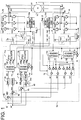
- FIG. 1 is a view showing an overall configuration of a control device for an AC rotary machine according to a first embodiment of this invention
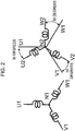
- Fig. 2 is a view illustrating a configuration of a three-phase AC power generator used as the AC rotary machine according to the first embodiment of this invention.
- An AC rotary machine 1a shown in Fig. 1 is a three-phase AC rotary machine in which, as shown in Fig. 2 , first three-phase windings U1, V1, W1 connected by a neutral point N1 and second three-phase windings U2, V2, W2 connected by a neutral point N2 are housed in a stator of a rotary machine without being electrically connected.
- FIG. 2 a case in which the first three-phase windings and the second three-phase windings are both connected in a Y connection is shown as an example of the AC rotary machine 1a, but this invention may also be applied to a ⁇ connection.
- a DC power supply 2a outputs a DC voltage Vdc1 to a first voltage application device 3a
- a DC power supply 2b outputs a DC voltage Vdc2 to a second voltage application device 3b.
- the DC power supplies 2a, 2b include all devices that output a DC voltage, such as a battery, a DC-DC converter, a diode rectifier, and a PWM rectifier.
- a configuration in which DC voltages are output to the first voltage application device 3a and the second voltage application device 3b using one of the DC power supplies 2a, 2b is also included in the scope of this invention.
- the first voltage application device 3a switches semiconductor switches Sup1, Sun1, Svp1, Svn1, Swp1, Swn1 (in the following description, these six semiconductor switches will be referred to as the semiconductor switches Sup1 to Swn1) ON and OFF by implementing PWM modulation on first voltage commands Vu1', Vv1', Vwl' using an inverse conversion circuit (an inverter). In so doing, the first voltage application device 3a power-converts the DC voltage Vdc1 input from the DC power supply 2a into an AC voltage, and applies the AC voltage to the first three-phase windings U1, V1, W1 of the AC rotary machine 1a.
- each of the semiconductor switches Sup1 to Swn1 is constituted by a semiconductor switch such as an IGBT, a bipolar transistor, or a MOS power transistor, and a diode connected in anti-parallel to the semiconductor switch.
- the second voltage application device 3b switches semiconductor switches Sup2, Sun2, Svp2, Svn2, Swp2, Swn2 (in the following description, these six semiconductor switches will be referred to as the semiconductor switches Sup2 to Swn2) ON and OFF by implementing PWM modulation on second voltage commands Vu2', Vv2', Vw2' using an inverse conversion circuit (an inverter).
- the second voltage application device 3b power-converts the DC voltage Vdc2 input from the DC power supply 2b into an AC voltage, and applies the AC voltage to the second three-phase windings U2, V2, W2 of the AC rotary machine 1a.
- each of the semiconductor switches Sup2 to Swn2 is constituted by a semiconductor switch such as an IGBT, a bipolar transistor, or a MOS power transistor, and a diode connected in anti-parallel to the semiconductor switch.
- a first current detector 4a uses a current sensor such as a shunt resistor or a current transformer (a CT) to detect a current Idc1 flowing through a first DC bus of a first power converter 3a.
- Fig. 3 is a view showing relationships between Idc1 and first voltage vectors V0 (1) to V7 (1) corresponding respectively to the ON/OFF conditions of the semiconductor switches Sup1 to Swn1, according to the first embodiment of this invention.
- “ 1 " indicates that a switch is switched ON, and "0" indicates that a switch is switched OFF.
- the first current detector 4a detects first three-phase currents Iu1, Iv1, Iw1 on the basis of the relationships shown in Fig. 3 . Note that the first current detector 4a may detect two phases of the first three-phase currents Iu1, Iv1, Iw1 from Idc1, and the remaining phase may be determined by calculation using the fact that the sum of the currents of the three phases is zero.
- a second current detector 4b uses a current sensor such as a shunt resistor or a current transformer (a CT) to detect a current Idc2 flowing through a second DC bus of a second power converter 3b.
- Fig. 4 is a view showing relationships between a current that is equal to Idc2 and second voltage vectors V0 (2) to V7 (2) corresponding respectively to the ON/OFF conditions of the semiconductor switches Sup2 to Swn2, according to the first embodiment of this invention.
- “ 1 " indicates that a switch is switched ON, and "0" indicates that a switch is switched OFF.
- the second current detector 4b detects second three-phase currents Iu2, Iv2, Iw2 on the basis of the relationships shown in Fig. 4 . Note that the second current detector 4b may detect two phases of the second three-phase currents Iu2, Iv2, Iw2 from Idc2, and the remaining phase may be determined by calculation using the fact that the sum of the currents of the three phases is zero.
- the numeral (1) in parentheses in the first voltage vectors shown in Fig. 3 and the numeral (2) in parentheses in the second voltage vectors shown in Fig. 4 are used to differentiate the first voltage vectors from the second voltage vectors. Hence, (1) is appended to the first voltage vectors based on the first voltage commands, and (2) is appended to the second voltage vectors based on the second voltage commands.
- a first detectability determination device 12a determines whether or not the first three-phase currents are detectable on the basis of the first voltage commands Vu1', Vv1', Vw1', and outputs a first detectability determination signal flag_1.
- a second detectability determination device 12b determines whether or not the second three-phase currents are detectable on the basis of the second voltage commands Vu2', Vv2', Vw2', and outputs a second detectability determination signal flag_2.
- a coordinate converter 6a calculates currents Id1, Iq1 of the first windings on two rotational axes by converting the first three-phase currents Iu1, Iv1, Iw1 detected by the first current detector 4a into currents on rotating coordinates on the basis of a rotation position ⁇ of the AC rotary machine 1a.
- a coordinate converter 6b calculates currents Id2, Iq2 of the second windings on two rotational axes by converting the second three-phase currents Iu2, Iv2, Iw2 detected by the second current detector 4b into currents on rotating coordinates on the basis of a position ⁇ -30 obtained by subtracting 30 degrees from the rotation position ⁇ of the AC rotary machine 1a.
- a switch 7a switches the currents Id1, Iq1 of the first windings so that the currents are output respectively as currents Id1', Iq1' on rotating two-axis coordinates.
- the switch 7a switches the currents Id2, Iq2 of the second windings so that the currents are output respectively as the currents Id1', Iq1' on rotating two-axis coordinates.
- the switch 7a switches the currents Id2, Iq2 of the second windings so that the currents are output respectively as currents Id2', Iq2' on rotating two-axis coordinates.
- the switch 7a switches the currents Id1, Iq1 of the first windings so that the currents are output respectively as the currents Id2', Iq2' on rotating two-axis coordinates.
- the currents Id1', Iq1' on rotating two-axis coordinates and the currents Id2', Iq2' on rotating two-axis coordinates respectively correspond to current detection values used to calculate voltage commands Vd1, Vq1 on rotating two-axis coordinates and voltage commands Vd2, Vq2 on rotating two-axis coordinates, as will be described below.
- the three-phase currents of the windings on the detectable side are used as is as the three-phase currents on the undetectable side, but the three-phase currents on the undetectable side may be determined using a different estimation method.
- a subtractor 8a calculates a deviation dId1 between a d axis current command Id* of the AC rotary machine 1a and the current Id1' on rotating two-axis coordinates, output by the switch 7a.
- a subtractor 8b calculates a deviation dIq1 between a q axis current command Iq* of the AC rotary machine 1a and the current Iq1' on rotating two-axis coordinates, output by the switch 7a.
- a subtractor 8c calculates a deviation dId2 between the d axis current command Id* of the AC rotary machine 1a and the current Id2' on rotating two-axis coordinates, output by the switch 7a.
- a subtractor 8d calculates a deviation dIq2 between the q axis current command Iq* of the AC rotary machine 1a and the current Iq2' on rotating two-axis coordinates, output by the switch 7a.
- a controller 9a calculates the voltage command Vd1 on rotating two-axis coordinates using a P controller and a PI controller so that the deviation dId1 is controlled to zero.
- a controller 9b calculates the voltage command Vq1 on rotating two-axis coordinates using a P controller and a PI controller so that the deviation dIq1 is controlled to zero.
- a controller 9c calculates the voltage command Vd2 on rotating two-axis coordinates using a P controller and a PI controller so that the deviation dId2 is controlled to zero.
- a controller 9d calculates the voltage command Vq2 on rotating two-axis coordinates using a P controller and a PI controller so that the deviation dIq2 is controlled to zero.
- a coordinate converter 10a calculates first voltage commands Vu1, Vv1, Vw1 by performing coordinate conversion to convert the voltage commands Vd1, Vq1 on rotating two-axis coordinates into three-phase AC coordinates on the basis of the rotation position ⁇ of the AC rotary machine 1a.
- a coordinate converter 10b calculates second voltage commands Vu2, Vv2, Vw2 by performing coordinate conversion to convert the voltage commands Vd2, Vq2 on rotating two-axis coordinates into three-phase AC coordinates on the basis of the position ⁇ -30 obtained by subtracting 30 degrees from the rotation position ⁇ of the AC rotary machine 1a.
- An offset calculator 11a adds an offset voltage Voffset1 to the first voltage commands Vu1, Vv1, Vw1, as shown below in Equations (1) to (3), and outputs the results as the first voltage commands Vu1', Vv1', Vwl'.
- Vu 1 ′ Vu 1 + Voffset 1
- Vv 1 ′ Vv 1 + Voffset 1
- Vw 1 ′ Vw 1 + Voffset 1
- An offset calculator 11b adds an offset voltage Voffset2 to the second voltage commands Vu2, Vv2, Vw2, as shown below in Equations (4) to (6), and outputs the results as the second voltage commands Vu2', Vv2', Vw2'.
- Vu 2 ′ Vu 2 + Voffset 2
- Vv 2 ′ Vv 2 + Voffset 2
- Vw 2 ′ Vw 2 + Voffset 2
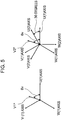
- Fig. 5 is an illustrative view showing a first voltage command vector V1* based on the first voltage commands Vu1', Vv1', Vw1' and a second voltage command vector V2* based on the second voltage commands Vu2', Vv2', Vw2', according to the first embodiment of this invention.
- the first voltage command vector V1* and the second voltage command vector V2* are vectors that rotate about a U(1)-V(1)-W(1) axis and a U(2)-V(2)-W(2) axis, respectively.
- numerals shown in parentheses in Fig. 5 denote either axes corresponding to the first windings or axes corresponding to the second windings. More specifically, U(1), V(1), W(1), to which (1) is appended, respectively denote axes corresponding to the U phase, the V phase, and the W phase of the first windings, while U(2), V(2), W(2), to which (2) is appended, respectively denote axes corresponding to the U phase, the V phase, and the W phase of the second windings.
- phase angles of the first voltage command vector V1* and the second voltage command vector V2* when the U(1) axis is used as a reference are both ⁇ v. In other words, no phase difference exists therebetween.
- Figs. 6A and 6B are waveform diagrams showing the first voltage commands Vu1, Vv1, Vw1 and the second voltage commands Vu2, Vv2, Vw2 according to the first embodiment of this invention.
- the U(2), V(2), and W(2) axes shown in Fig. 5 are respectively retarded by a phase of 30 degrees relative to the U(1), V(1), and W(1) axes. Therefore, as shown in Figs. 6A and 6B , the second voltage commands Vu2, Vv2, Vw2 are respectively retarded by a phase of 30 degrees relative to the first voltage commands Vu1, Vv1, Vw1.
- the abscissa shows the voltage phase angle ⁇ v when the U(1) axis is used as a reference.
- the AC rotary machine 1a in which a 30 degree phase difference exists between the first windings and the second windings, a 30 degree phase difference exists between the first voltage commands and the second voltage commands.
- a phase difference of 30 + 60 ⁇ N (where N is an integer) degrees exists between the first windings and the second windings
- a 30 + 60 ⁇ N degree phase difference exists between the first voltage commands and the second voltage commands.
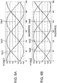
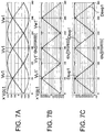
- Figs. 7A-7C are views illustrating relationships between the voltage commands and ON ratios of upper side arm elements of the respective phases with respect to the first voltage application device 3a, according to the first embodiment of this invention.
- Fig. 7A shows the first voltage commands Vu1, Vv1, Vw1 shown in Figs. 6A and 6B , which are output by the coordinate converter 10a.
- Fig. 7B shows the first voltage commands Vu1', Vv1', Vwl' serving as the output of the offset calculator 11a, which are calculated using Equations (1) to (3).
- Equation (7) The offset voltage Voffset1 of Equations (1) to (3) is given by Equation (7), shown below, using a maximum value Vmax1 and a minimum value Vmin1 of the first voltage commands Vu1, Vv1, Vw1.
- Voffset 1 ⁇ 0.5 Vmin 1 + Vmax 1
- a voltage output range of a phase voltage that can be output by the first voltage application device 3a extends from zero to the bus voltage Vdc1. Therefore, when the first voltage commands Vu1', Vv1', Vwl' are smaller than -0.5 Vdc1 or exceed 0.5 Vdc1, the first voltage commands Vu1', Vv1', Vwl' are limited to -0.5 Vdc1 or 0.5 Vdc1 so that the width of the voltage output range remains within the voltage Vdc1 that can be output by the first voltage application device 3a.
- Voffset1 may be determined using another offset voltage calculation method such as a two phase modulation method or a third harmonic wave superimposing method instead of Equation (7).
- Fig. 7C shows ON duties Dsup1, Dsvp1, Dswp1 denoting the ON ratios of the upper side arm elements (Sup1, Svp1, Swp1) of the respective phases in the first voltage application device 3a.
- Dsup1 is 0.6
- the first voltage application device 3a sets the ON ratio of Sup1 within the switching period Tsw at 0.6.
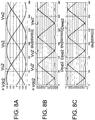
- Figs. 8A-8C are views illustrating relationships between the voltage commands and the ON ratios of the upper side arm elements of the respective phases with respect to the second voltage application device 3b, according to the first embodiment of this invention.
- Fig. 8A shows the second voltage commands Vu2, Vv2, Vw2 shown in Figs. 6A and 6B , which are output by the coordinate converter 10b.
- Fig. 8B shows the second voltage commands Vu2', Vv2', Vw2' serving as the output of the offset calculator 11b, which are calculated using Equations (4) to (6).
- Equation (11) The offset voltage Voffset2 of Equations (4) to (6) is given by Equation (11), shown below, using a maximum value Vmax2 and a minimum value Vmin2 of the second voltage commands Vu2, Vv2, Vw2.
- Voffset 2 ⁇ 0.5 Vmin 2 + Vmax 2
- the voltage output range of the phase voltage that can be output by the second voltage application device 3b extends from zero to the bus voltage Vdc2. Therefore, when the second voltage commands Vu2', Vv2', Vw2' are smaller than -0.5 Vdc2 or exceed 0.5 Vdc2, the second voltage commands Vu2', Vv2', Vw2' are limited to -0.5 Vdc2 or 0.5 Vdc2 so that the width of the voltage output range remains within the voltage Vdc2 that can be output by the second voltage application device 3b.
- Voffset2 may be determined using another offset voltage calculation method such as a two phase modulation method or a third harmonic wave superimposing method instead of Equation (11).
- Fig. 8C shows ON duties Dsup2, Dsvp2, Dswp2 denoting the ON ratios of the upper side arm elements (Sup2, Svp2, Swp2) of the respective phases in the second voltage application device 3b.
- Dsup2 is 0.6
- the second voltage application device 3b sets the ON ratio of Sup2 within the switching period Tsw at 0.6.
- Equation (12) to (14) are established between the ON duties (Dsup2, Dsvp2, Dswp2) of the upper side arm elements of the respective phases and ON duties (Dsun2, Dsvn2, Dswn2) of the lower side arm elements.
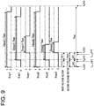
- Fig. 9 is an operational diagram relating to ON/OFF patterns of the semiconductor switches and current detection timings of the current detectors 4a, 4b, according to the first embodiment of this invention. More specifically, Fig. 9 is a view showing relationships between the ON/OFF patterns of the semiconductor switches Sup1, Svp1, Swp1 of the first voltage application device 3a and the semiconductor switches Sup2, Svp2, Swp2 of the second voltage application device 3b and the current detection timings of the current detectors 4a, 4b within the period (a PWM period) Tsw of a switching signal.
- Sun1, Svn1, Swn1 and Sun2, Svn2, Swn2 have inverse relationships to Sup1, Svp1, Swp1 and Sup2, Svp2, Swp2, respectively (i.e. 0 in place of 1 and 1 in place of 0, excluding a dead time period), and are not therefore shown in the drawing.
- Equations (18) to (20) are assumed to be established.
- Emax 2 Vu 2 ′
- Emid 2 Vv 2 ′
- Emin 2 Vw 2 ′
- the first voltage vector and the second voltage vector are at V1 (1) and V1 (2), respectively, between the times t1 (n) and t2 (n).
- the current detectors 4a, 4b detect Idc1 and Idc2 at a time ts1-1 (n) between the times t1 (n) and t2 (n).
- the first voltage vector is at V1 (1) between the times t1 (n) and t2 (n), and therefore Idc1, detected at the time ts1-1 (n), is equal to Iu1.
- the second voltage vector is at V1 (2) between the times t1 (n) and t2 (n), and therefore Idc2, detected at the time ts1-1 (n), is equal to Iu2.
- the first voltage vector and the second voltage vector are at V2 (1) and V2 (2), respectively, between the times t2 (n) and t3 (n).
- the current detectors 4a, 4b detect Idc1 and Idc2 again at a time ts1-2 (n) between the times t2 (n) and t3 (n).
- the time shift ⁇ t2, similarly to the time shift ⁇ t1, is set to equal or exceed the "first predetermined value".
- the first voltage vector is at V2 (1) between the times t2 (n) and t3 (n), and therefore Idc1, detected at the time ts1-2 (n), is equal to -Iw1.
- the second voltage vector is at V2 (2) between the times t2 (n) and t3 (n), and therefore Idc2, detected at the time ts1-2 (n), is equal to -Iw2.
- Swp1 and Swp2 are set at 1. Respective pulse widths (periods during which "1" is maintained) of Sup1 to Swp2 are determined from products of the ON duties Dsup1 to Dswp2 corresponding to the respective switches and the switching period Tsw.
- the switch of the upper side arm element of the phase corresponding to the first maximum phase voltage Emax1, the switch of the upper side arm element of the phase corresponding to the first intermediate phase voltage Emid1, and the switch of the upper side arm element of the phase corresponding to the first minimum phase voltage Emin1 are switched ON in that order at time shifts of ⁇ t1 or ⁇ t2, which are set to equal or exceed the first predetermined value.
- the two first voltage vectors shown in Fig. 3 with which two phases of the first three-phase currents Iu1, Iv1, Iw1 can be detected from Idc1 are formed and the two second voltage vectors shown in Fig. 4 , with which two phases of the second three-phase currents Iu2, Iv2, Iw2 can be detected from Idc2, are formed.
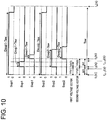
- Fig. 10 is a different operational diagram to Fig. 9 relating to the ON/OFF patterns of the semiconductor switches and the current detection timings of the current detectors 4a, 4b according to the first embodiment of this invention.
- Fig. 10 shows an example of a case in which the first three-phase currents Iu1, Iv1, Iw1 cannot be detected.
- Fig. 10 shows a condition in which Vv1' is small such that Dsvp1 ⁇ Tsw is smaller than ⁇ t2.
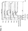
- Fig. 11 is a different operational diagram to Figs. 9 and 10 relating to the ON/OFF patterns of the semiconductor switches and the current detection timings of the current detectors 4a, 4b according to the first embodiment of this invention.
- Fig. 11 shows an example of a case in which the first three-phase currents Iu1, Iv1, Iw1 cannot be detected.
- Fig. 11 shows a condition in which Vv1' is large such that Dsvp1 ⁇ Tsw is larger than Tsw - ⁇ t1.
- Vv1' is large such that Dsvp1 ⁇ Tsw is larger than Tsw - ⁇ t1.
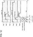
- Fig. 12 is a different operational diagram to Figs. 10 and 11 relating to the ON/OFF patterns of the semiconductor switches and the current detection timings of the current detectors 4a, 4b according to the first embodiment of this invention.
- Fig. 12 shows an example of a case in which the second three-phase currents Iu2, Iv2, Iw2 cannot be detected.
- Vv2' is small, V2 (2) cannot be formed over the duration of the time shift ⁇ t2.
- Fig. 13 is a different operational diagram to Fig. 12 relating to the ON/OFF patterns of the semiconductor switches and the current detection timings of the current detectors 4a, 4b according to the first embodiment of this invention.
- Fig. 13 shows an example of a case in which the second three-phase currents Iu2, Iv2, Iw2 cannot be detected.
- Vv2' is large, V1 (2) cannot be formed over the duration of the time shift ⁇ t1.
- the switching frequency is set to be no lower than 20 kHz (i.e. outside the band of the audible range).
- the audible range of a human being is between 20 Hz and 20 kHz, and therefore, by setting the switching frequency to be no lower than 20 kHz (i.e. outside the band of the audible range), the sound of the switching frequency component cannot be heard by human ears.
- the switching frequency is reduced below 20 kHz in order to secure the time shift ⁇ t1 and the time shift ⁇ t2, however, the sound of the switching frequency component can be heard by human ears as noise.
- a technical feature of this invention is that Idc2 is detected with a high degree of precision even when it is accepted that Idc1 cannot be detected due to the magnitude of the first intermediate phase voltage Emid1, and Idc1 is detected with a high degree of precision even when it is accepted that Idc2 cannot be detected due to the magnitude of the second intermediate phase voltage Emid2.
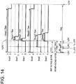
- Fig. 14 is an operational diagram relating to the ON/OFF patterns of the semiconductor switches and the current detection timings of the current detectors 4a, 4b according to the first embodiment of this invention.
- Fig. 14 shows an operation for solving the problem illustrated in Fig. 10 . More specifically, in Fig. 14 , the ON timing of Svp1 is shifted from t2 (n) in Fig. 10 to t5 (n).
- t5 (n) is set to be within a "second predetermined value" of the timing t3 (n) at which the first minimum phase voltage is switched ON.
- the "second predetermined value” is a smaller value than the "first predetermined value”, and a smaller value than an interval between ts1-2 (n), which serves as a bus current detection timing, and t3 (n), i.e. the ON timing of the first minimum phase voltage.
- t3 (n) and t5 (n) may be set to match, or in other words such that the first intermediate phase voltage and the first minimum phase voltage are switched ON simultaneously.
- the ON time of the first intermediate phase voltage takes a value that is equal to or smaller than ⁇ t2, as illustrated above in Fig. 10 , the ON time of the first intermediate phase voltage is set to be within the second predetermined value of the ON time of the first minimum phase voltage, as shown in Fig. 14 .
- the first voltage application device 3a does not perform switching in the vicinity of ts1-2 (n), and as a result, Idc2 can be detected at ts1-2 (n) with a higher degree of precision than in Fig. 10 .
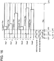
- Fig. 15 is an operational diagram relating to the ON/OFF patterns of the semiconductor switches and the current detection timings of the current detectors 4a, 4b according to the first embodiment of this invention.
- Fig. 15 shows an operation for solving the problem illustrated in Fig. 11 . More specifically, in Fig. 15 , the ON timing of Svp1 is shifted from t2 (n) in Fig. 11 to t6 (n).
- t6 (n) is set to be within the "second predetermined value" of the timing t1 (n) at which the first maximum phase voltage is switched ON. Note that t1 (n) and t6 (n) may be set to match, or in other words such that the first intermediate phase voltage and the first maximum phase voltage are switched ON simultaneously.
- the ON time of the first intermediate phase voltage takes a value that is equal to or smaller than ⁇ t2, as illustrated above in Fig. 11 , the ON time of the first intermediate phase voltage is set to be within the second predetermined value of the ON time of the first maximum phase voltage, as shown in Fig. 15 .
- the first voltage application device 3a does not perform switching in the vicinity of ts1-1 (n), and as a result, Idc2 can be detected at ts1-1 (n) with a higher degree of precision than in Fig. 11 .
- Fig. 16 is a different operational diagram to Fig. 9 relating to the ON/OFF patterns of the semiconductor switches and the current detection timings of the current detectors 4a, 4b according to the first embodiment of this invention.
- Fig. 16 similarly to Fig. 9 , when the first maximum phase voltage Emax1, the first intermediate phase voltage Emid1, and the first minimum phase voltage Emin1 are set in descending order in relation to the first voltage commands Vu1', Vv1', Vw1', the relationships shown above in Equations (15) to (17) are assumed to be established, and when the second maximum phase voltage Emax2, the second intermediate phase voltage Emid2, and the second minimum phase voltage Emin2 are set in descending order in relation to the second voltage commands Vu2', Vv2', Vw2', the relationships shown above in Equations (18) to (20) are assumed to be established.
- the first voltage vector and the second voltage vector are at V2 (1) and V2 (2), respectively, between the times t1 (n) and t2 (n).
- the current detectors 4a, 4b detect Idc1 and Idc2 at the time ts1-1 (n) between the times t1 (n) and t2 (n).
- the first voltage vector is at V2 (1) between the times t1 (n) and t2 (n), and therefore Idc1, detected at the time ts1-1 (n), is equal to -Iw1.
- the second voltage vector is at V2 (2) between the times t1 (n) and t2 (n), and therefore Idc2, detected at the time ts1-1 (n), is equal to -Iw2.
- the first voltage vector and the second voltage vector are at V1 (1) and V1 (2), respectively, between the times t2 (n) and t3 (n).
- the current detectors 4a, 4b detect Idc1 and Idc2 again at the time ts1-2 (n) between the times t2 (n) and t3 (n).
- the first voltage vector is at V1 (1) between the times t2 (n) and t3 (n), and therefore Idc1, detected at the time ts1-2 (n), is equal to Iu1.
- the second voltage vector is at V1 (2) between the times t2 (n) and t3 (n), and therefore Idc2, detected at the time ts1-2 (n), is equal to Iu2.
- Sup1 and Sup2 are set at 1. Respective times during which Sup1 to Swp2 are maintained at "0" are determined from products of the switching period Tsw and values obtained by subtracting the ON duties Dsup1 to Dswp2 corresponding to the respective switches from 1.
- the switch of the upper side arm element of the phase corresponding to the first minimum phase voltage Emin1 the switch of the upper side arm element of the phase corresponding to the first intermediate phase voltage Emid1
- the switch of the upper side arm element of the phase corresponding to the first maximum phase voltage Emax1 are switched OFF in that order at time shifts of ⁇ t1 or ⁇ t2, which are set to equal or exceed the first predetermined value.
- the two first voltage vectors shown in Fig. 3 with which two phases of the first three-phase currents Iu1, Iv1, Iw1 can be detected from Idc1 are formed and the two second voltage vectors shown in Fig. 4 , with which two phases of the second three-phase currents Iu2, Iv2, Iw2 can be detected from Idc2, are formed.
- Fig. 17 is a different operational diagram to Fig. 16 relating to the ON/OFF patterns of the semiconductor switches and the current detection timings of the current detectors 4a, 4b according to the first embodiment of this invention.
- Fig. 17 shows an example of a case in which the first three-phase currents Iu1, Iv1, Iw1 cannot be detected.
- Fig. 17 shows a condition in which Vv1' is small such that Dsvp1 ⁇ Tsw is smaller than ⁇ t1.
- the OFF timing of Svp1 is between t1 (n) and t2 (n), and therefore approaches ts1-1 (n), i.e. the detection timing of Idc2.
- noise may occur while detecting Idc2 due to the switching operation for switching Svp1 OFF, and as a result, it may be impossible to detect Idc2 correctly during ⁇ t2.
- Fig. 18 is a different operational diagram to Figs. 16 and 17 relating to the ON/OFF patterns of the semiconductor switches and the current detection timings of the current detectors 4a, 4b according to the first embodiment of this invention.
- Fig. 18 shows an example of a case in which the first three-phase currents Iu1, Iv1, Iw1 cannot be detected.
- Fig. 18 shows a condition in which Vv1' is large such that (1 - Dsvp1) ⁇ Tsw, i.e. the OFF time of Svp1, is smaller than ⁇ t2.
- Vv1' is large such that (1 - Dsvp1) ⁇ Tsw, i.e. the OFF time of Svp1, is smaller than ⁇ t2.
- Svp1 is switched OFF at the time t2 (n) in this condition, Svp1 is switched ON before the time t3 (n), and therefore the first voltage vector V1 (1) cannot be formed over the duration of the time shift ⁇ t2.
- Idc1 cannot be detected during ⁇ t2.
- the ON timing of Svp1 is between t2 (n) and t3 (n), and therefore approaches ts1-2 (n), i.e. the detection timing of Idc2.
- noise may occur while detecting Idc2 due to the switching operation for switching Svp1 ON, and as a result, it may be impossible to detect Idc2 correctly during ⁇ t2.
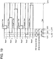
- Fig. 19 is a different operational diagram to Figs. 17 and 18 relating to the ON/OFF patterns of the semiconductor switches and the current detection timings of the current detectors 4a, 4b according to the first embodiment of this invention.
- Fig. 19 shows an example of a case in which the second three-phase currents Iu2, Iv2, Iw2 cannot be detected.
- Vv2' is small
- V2 (2) cannot be formed over the duration of the shift time ⁇ t1, and as a result, Idc2 cannot be detected during ⁇ t1.
- the OFF timing of Svp2 is between t1 (n) and t2 (n), and therefore approaches ts1-1 (n), i.e. the detection timing of Idc1.
- noise may occur while detecting Idc1 due to the switching operation for switching Svp2 OFF, and as a result, it may be impossible to detect Idc1 correctly during ⁇ t1.
- Fig. 20 is a different operational diagram to Fig. 19 relating to the ON/OFF patterns of the semiconductor switches and the current detection timings of the current detectors 4a, 4b according to the first embodiment of this invention.
- Fig. 20 shows an example of a case in which the second three-phase currents Iu2, Iv2, Iw2 cannot be detected.
- Vv2' is large, V1 (2) cannot be formed over the duration of the shift time ⁇ t2, and as a result, Idc2 cannot be detected during ⁇ t2.
- the ON timing of Svp2 is between t2 (n) and t3 (n), and therefore approaches ts1-2 (n), i.e. the detection timing of Idc1.
- noise may occur while detecting Idc1 due to the switching operation for switching Svp2 ON, and as a result, it may be impossible to detect Idc1 correctly during ⁇ t2.
- Fig. 21 is an operational diagram relating to the ON/OFF patterns of the semiconductor switches and the current detection timings of the current detectors 4a, 4b according to the first embodiment of this invention.
- Fig. 21 shows an operation for solving the problem illustrated in Fig. 17 . More specifically, in Fig. 21 , the OFF timing of Svp1 is shifted to t7 (n) from Fig. 17 .
- t7 (n) is set to be within the "second predetermined value" of the timing t4 (n) at which the first minimum phase voltage is switched OFF.
- the OFF time of the first intermediate phase voltage is set to be within the second predetermined value of the OFF time of the first minimum phase voltage.
- Fig. 22 is an operational diagram relating to the ON/OFF patterns of the semiconductor switches and the current detection timings of the current detectors 4a, 4b according to the first embodiment of this invention.
- Fig. 22 shows an operation for solving the problem illustrated in Fig. 18 . More specifically, in Fig. 22 , the OFF timing of Svp1 is shifted to t8 (n) from Fig. 18 .
- t8 (n) is set to be within the "second predetermined value" of the timing t3 (n) at which the first maximum phase voltage is switched ON.
- the OFF time of the first intermediate phase voltage is set to be within the second predetermined value of the OFF time of the first maximum phase voltage.
- Figs. 14 , 15 , 21 , and 22 illustrate methods with which Idc2 can be detected with a high degree of precision at ts1-1 (n) or ts1-2 (n) in a case where the first intermediate phase voltage Emid1 cannot be secured for the duration of the time shift ⁇ t1 or ⁇ t2.
- Idc1 rather than Idc2
- Idc1 can be detected with a high degree of precision at ts1-1 (n) or ts1-2 (n) in a case where the second intermediate phase voltage Emid2 cannot be secured for the duration of the time shift ⁇ t1 or ⁇ t2.
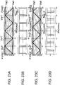
- FIGs. 23A-23D are illustrative views relating to functions of the first detectability determination device 12a and the second detectability determination device 12b according to the first embodiment of this invention.
- the first detectability determination device 12a determines whether or not the first current detector 4a can detect the first three-phase currents by determining whether or not the voltage command value of the phase corresponding to the first intermediate phase voltage Emid1 is within a range extending from a third predetermined value Vs3 down to a fourth predetermined value Vs4.
- the second detectability determination device 12b determines whether or not the second current detector 4b can detect the second three-phase currents by determining whether or not the voltage command value of the phase corresponding to the second intermediate phase voltage Emid2 is within a range extending from the third predetermined value Vs3 down to the fourth predetermined value Vs4.
- the third predetermined value Vs3 corresponds to an upper limit value at which the time shift ⁇ t1 can be secured.
- the fourth predetermined value Vs4 serves as a lower limit value at which the time shift ⁇ t2 can be secured.
- a dotted line indicates the first voltage commands Vu1', Vv1', Vwl' shown in Fig. 7B
- a solid line indicates the first intermediate phase voltage Emid1
- dot-dash lines indicate the third predetermined value Vs3 and the fourth predetermined value Vs4.
- Vs 1 0.4 Vdc 1
- Vs 2 ⁇ 0.4 Vdc 1
- Fig. 23B shows the output of the first detectability determination device 12a.
- the first detectability determination device 12a determines whether or not the first three-phase currents can be detected by determining whether or not the first intermediate phase voltage Emid1 is within the range extending from the third predetermined value Vs3 down to the fourth predetermined value Vs4.
- the first detectability determination device 12a outputs the first detectability determination signal flag_1 at 1 when the first intermediate phase voltage Emid1 is within the range extending from the third predetermined value Vs3 down to the fourth predetermined value Vs4, and at 0 when the first intermediate phase voltage Emid1 is outside this range.
- a dotted line indicates the second voltage commands Vu2', Vv2', Vw2' shown in Fig. 8B
- a solid line indicates the second intermediate phase voltage Emid2
- dot-dash lines indicate the third predetermined value Vs3 and the fourth predetermined value Vs4.
- Fig. 23D shows the output of the second detectability determination device 12b.
- the second detectability determination device 12b determines whether or not the second three-phase currents can be detected by determining whether or not the second intermediate phase voltage Emid2 is within the range extending from the third predetermined value Vs3 down to the fourth predetermined value Vs4, and outputs the second detectability determination signal flag_2 at 1 when the second intermediate phase voltage Emid2 is within the range extending from the third predetermined value Vs3 down to the fourth predetermined value Vs4, and at 0 when the second intermediate phase voltage Emid2 is outside this range.
- the first detectability determination signal flag_1 shifts to 0 in the vicinity of a voltage phase angle ⁇ v of 60 ⁇ x (where x is 0, 1, 2, 3, 4, 5, 6).
- the second detectability determination signal flag_2 shifts to 0 in the vicinity of a voltage phase angle ⁇ v of 30 + 60 ⁇ x (where x is 0, 1, 2, 3, 4, 5).
- the voltage phase angles ⁇ v at which the first detectability determination signal flag_1 and the second detectability determination signal flag_2 shift to 0 deviate from each other by 30 degrees, and therefore, when flag_1 is at 0, flag_2 is at 1, and conversely when flag_2 is at 0, flag_1 is at 1. It is therefore evident that flag_1 and flag_2 are never at 0 simultaneously, and at least one thereof is at 1.
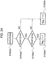
- Fig. 24 is a flowchart showing a series of operations executed by the first detectability determination device 12a according to the first embodiment of this invention.
- the first detectability determination device 12a calculates the first intermediate phase voltage Emid1 on the basis of the first voltage commands Vu1', Vv1', Vw1'.
- step S1000b the first detectability determination device 12a determines whether or not the first intermediate phase voltage Emid1 is equal to or smaller than the third predetermined value Vs3.
- step S1000c the routine advances to step S1000c, and when "NO” is obtained, the routine advances to step S1000e.
- the first detectability determination device 12a determines whether or not the first intermediate phase voltage Emid1 equals or exceeds the fourth predetermined value Vs4. When “YES” is obtained, the routine advances to step S1000d, and when "NO” is obtained, the routine advances to step S1000e.
- the first detectability determination device 12a inserts 1 into the first detectability determination signal flag_1.
- the first detectability determination device 12a inserts 0 into the first detectability determination signal flag_1.
- Fig. 25 is a flowchart showing a series of operations executed by the second detectability determination device 12b according to the first embodiment of this invention.
- the second detectability determination device 12b calculates the second intermediate phase voltage Emid2 on the basis of the second voltage commands Vu2', Vv2', Vw2'.
- step S2000b the second detectability determination device 12b determines whether or not the second intermediate phase voltage Emid2 is equal to or smaller than the third predetermined value Vs3.
- step S2000c the routine advances to step S2000c, and when "NO” is obtained, the routine advances to step S2000e.
- step S2000c the second detectability determination device 12b determines whether or not the second intermediate phase voltage Emid2 equals or exceeds the fourth predetermined value Vs4.
- step S2000d the routine advances to step S2000d, and when "NO” is obtained, the routine advances to step S2000e.
- the second detectability determination device 12b inserts 1 into the second detectability determination signal flag_2.
- the second detectability determination device 12b inserts 0 into the second detectability determination signal flag_2.
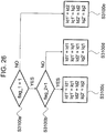
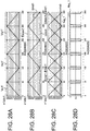
- Fig. 26 is a flowchart showing a series of operations executed by the switch 7a according to the first embodiment of this invention.
- the switch operation implemented by the switch 7a branches to steps S3100c, S3100d, and S3100e depending on a determination result obtained in step S3100a as to whether or not the first detectability determination signal flag_1 is equal to 1 and a determination result obtained in step S3100b as to whether or not the second detectability determination signal flag_2 is equal to 1.
- step S3100c the currents Id1, Iq1 of the first windings and the currents Id2, Iq2 of the second windings are selected as Id1', Iq1' and Id2', Iq2', respectively, and output.
- step S3100d the currents Id1, Iq1 of the first windings are selected as both Id1', Iq1' and Id2', Iq2' and output.
- step S3100e When flag_1 is not equal to 1, the routine advances to step S3100e regardless of the value of flag_2, where the currents Id2, Iq2 of the second windings are selected as both Id1', Iq1' and Id2', Iq2' and output.
- the first voltage application device 3a applies voltages to the first three-phase windings at ON intervals ( ⁇ t1, ⁇ t2) equaling or exceeding the first predetermined value.
- this invention may also be employed in a case in which voltages are applied at OFF intervals equaling or exceeding the first predetermined value.
- the first intermediate phase voltage is modified so as to be switched ON at a timing within the second predetermined value of the first maximum phase voltage when the first intermediate phase voltage is larger than the first predetermined value.
- the first minimum phase voltage may be modified in addition to the first intermediate phase voltage so as to be switched ON at a timing within the second predetermined value of the first maximum phase voltage.
- the ON or OFF interval can be set within the second predetermined value with respect to at least two phases in a case where the currents of the first three-phase windings or the currents of the second three-phase windings are determined to be undetectable.
- switching by the voltage application device at the current detection timing can be avoided without lengthening the switching period Tsw, as in PTL 1, and without the need to limit the amplitudes of the first voltage commands to a range in which the first intermediate phase voltage can be secured over the duration of the time shifts.
- the output of the AC rotary machine 1a can be increased while keeping the noise generated thereby low.
- calculation processing implemented by a first detectability determination device 12c differs from that of the first detectability determination device 12a according to the first embodiment. Accordingly, the following description focuses on the calculation processing executed by the first detectability determination device 12c according to the second embodiment.
- Fig. 27 is a flowchart showing a series of operations executed by the first detectability determination device 12c according to the second embodiment of this invention.
- the first detectability determination device 12c calculates the first maximum phase voltage Emax1, the first intermediate phase voltage Emid1, and the first minimum phase voltage Emin1 on the basis of the first voltage commands Vu1', Vv1', Vwl'.
- step S4000b the first detectability determination device 12c determines whether or not a difference (Emax1 - Emid1) between the first maximum phase voltage and the first intermediate phase voltage equals or exceeds a fifth predetermined value Vs5.
- a difference Emax1 - Emid1
- Vs5 a fifth predetermined value
- the first detectability determination device 12c determines whether or not a difference (Emid1 - Emin1) between the first intermediate phase voltage and the first minimum phase voltage equals or exceeds the fifth predetermined value Vs5.
- a difference Emid1 - Emin1
- the first detectability determination device 12c inserts 1 into the first detectability determination signal flag_1.
- the first detectability determination device 12c inserts 0 into the first detectability determination signal flag_1.
- Figs. 28A-28D are views showing waveforms corresponding to the respective steps of Fig. 27 in a case where the fifth predetermined value Vs5 is set at 0.1 Vdc, according to the second embodiment of this invention.
- Fig. 28A shows waveforms of the first voltage commands Vu1', Vv1', Vw1'
- Fig. 28B shows respective waveforms of the first maximum phase voltage Emax1, the first intermediate phase voltage Emid1, and the first minimum phase voltage Emin1, corresponding to step S4000a.
- Fig. 28C shows respective waveforms of the difference Emax1 - Emid1 between the first maximum phase voltage and the first intermediate phase voltage, corresponding to step S4000b, and the difference Emid1 - Emin1 between the first intermediate phase voltage and the first minimum phase voltage, corresponding to step S4000c. Further, Fig. 28D shows a waveform of the first detectability determination signal flag_1, corresponding to steps S4000d and S4000e.
- the respective differences between the first maximum phase voltage and the first intermediate phase voltage and between the first intermediate phase voltage and the first minimum phase voltage are calculated, and when the values thereof are smaller than the fifth predetermined value, the first three-phase currents are determined to be undetectable.
- the first three-phase currents are determined to be undetectable.
- the first detectability determination device 12c determines whether or not the first three-phase currents are detectable on the basis of the first voltage commands Vu1', Vv1', Vwl' serving as the output of the offset calculator 11a.
- identical calculation results are obtained for Emax1 - Emid1 and Emid1 - Emin1 when Emax1 - Emid1 and Emid1 - Emin1 are calculated on the basis of the first voltage commands Vu1, Vv1, Vw1 serving as the input of the offset calculator 11a instead of the first voltage commands Vu1', Vv1', Vwl'.
- the calculations implemented by the first detectability determination device 12c were described.
- the second detectability determination signal flag_2 can be obtained by implementing the calculations shown in Fig. 27 in a similar manner to the first detectability determination device 12c using the second voltage commands Vu2', Vv2', Vw2'.
- calculation processing implemented by a first detectability determination device 12d differs from that of the first detectability determination device 12a according to the first embodiment. Accordingly, the following description focuses on the calculation processing executed by the first detectability determination device 12d according to the third embodiment.
- the first detectability determination device 12d calculates the voltage phase angle ⁇ v on the basis of the first voltage commands Vu1', Vv1', Vwl' using Equation (21), shown below, and determines whether or not the first three-phase currents are detectable in accordance with a region of the voltage phase angle ⁇ v.
- ⁇ v arctan 3 2 V v 1 ′ ⁇ V w 1 ′ V u 1 ′ ⁇ 0.5 V v 1 ′ ⁇ 0.5 V w 1 ′
- the first three-phase currents are determined to be undetectable when the voltage phase angle ⁇ v is in the vicinity of 60 ⁇ x (where x is 0, 1, 2, 3, 4, 5, 6).
- ⁇ v calculated on the basis of the first voltage commands is within a range of no less than 60 ⁇ x - ⁇ and no more than 60 ⁇ x + ⁇ (where ⁇ is a margin)
- the first detectability determination device 12d determines that the first three-phase currents are undetectable and outputs 0 as flag_1.
- ⁇ v is outside this range, on the other hand, the first detectability determination device 12d determines that the first three-phase currents are detectable and outputs 1 as flag_1.
- the margin ⁇ is determined from the time shifts ⁇ t1 and ⁇ t2, a maximum value of the first voltage command, and so on, but the magnitude thereof does not exceed 30 degrees.
- the second three-phase currents are determined to be undetectable when the voltage phase angle ⁇ v is in the vicinity of 30 + 60 ⁇ x (where x is 0, 1, 2, 3, 4, 5).
- ⁇ v calculated on the basis of the first voltage commands is within a range of no less than 30 + 60 ⁇ x - ⁇ and no more than 30 + 60 ⁇ x + ⁇ (where ⁇ is a margin)
- the second detectability determination device 12b determines that the second three-phase currents are undetectable and outputs 0 as flag_2.
- ⁇ v is outside this range, on the other hand, the second detectability determination device 12b determines that the second three-phase currents are detectable and outputs 1 as flag_2.
- the first detectability determination device 12d determines whether or not the first three-phase currents are detectable on the basis of the first voltage commands Vu1', Vv1', Vwl' serving as the output of the offset calculator 11a.
- an identical result to the calculation result obtained from Equation (21) is obtained when the detectability of the first three-phase currents is calculated on the basis of the first voltage commands Vu1, Vv1, Vw1 serving as the input of the offset calculator 11a instead of the first voltage commands Vu1', Vv1', Vw1'.
- the first detectability determination device 12d may determine the voltage phase angle ⁇ v on the basis of the second voltage commands Vu2', Vv2', Vw2' instead of the first voltage commands Vu1, Vv1, Vw1 using Equation (22), shown below.
- the voltage phase angle ⁇ v may also be calculated using the second voltage commands Vu2, Vv2, Vw2 and the voltage commands Vd2, Vq2 on two rotational axes.
- Equation (21) and Equation (22) Furthermore, by calculating both Equation (21) and Equation (22) and using an average value thereof to determine the detectability of the first three-phase currents or the detectability of the second three-phase currents, an effect of suppressing a noise component included in the voltage phase angle ⁇ v can be obtained.
- Fig. 29 is a view showing an overall configuration of a control device for an AC rotary machine according to a fourth embodiment of this invention.
- the fourth embodiment differs from the first embodiment in that a control unit 5b is used instead of the control unit 5a. Accordingly, the following description focuses on modifications applied to the control unit 5a to obtain the control unit 5b.
- An adder 801a outputs an added value (Id1' + Id2') obtained by adding together the current Id1' on two rotational axes and the current Id2' on two rotational axes.
- An adder 801b outputs an added value (Iq1' + Iq2') obtained by adding together the current Iq1' on two rotational axes and the current Iq2' on two rotational axes.
- a subtractor 802a outputs a value (Id1' - Id2') obtained by subtracting the current Id2' on two rotational axes from the current Id1' on two rotational axes.
- a subtractor 802b outputs a value (Iq1' - Iq2') obtained by subtracting the current Iq2' on two rotational axes from the current Iq1' on two rotational axes.
- a multiplier 803a multiplies the added value (Id1' + Id2') output by the adder 801a by K1, and outputs the result as a sum current Id_sum.
- K1 0.5.
- a multiplier 803b multiplies the added value (Iq1' + Iq2') output by the adder 801b by K1, and outputs the result as a sum current Iq_sum.
- K1 0.5.
- a multiplier 804a multiplies the subtracted value (Id1' - Id2') output by the subtractor 802a by K2, and outputs the result as a differential current delta_Id.
- K2 0.5.
- a multiplier 804b multiplies the subtracted value (Iq1' - Iq2') output by the subtractor 802b by K2, and outputs the result as a differential current delta_Iq.
- K2 0.5.
- a subtractor 805a calculates a deviation dId_sum between the d axis current command Id* of the AC rotary machine 1a and the sum current Id_sum.
- a subtractor 805b calculates a deviation dIq_sum between the q axis current command Iq* of the AC rotary machine 1a and the sum current Iq_sum.
- a controller 806a outputs a sum voltage Vd_sum at which the deviation dId_sum is controlled to zero using a P controller, a PI controller, and the like on the basis of a product of a proportional gain Kpd_sum of the used controllers and the deviation dId_sum.
- a controller 806b outputs a sum voltage Vd_sum at which the deviation dIq_sum is controlled to zero using a P controller, a PI controller, and the like on the basis of a product of a proportional gain Kpq_sum of the used controllers and the deviation dIq_sum.
- a controller 806c outputs a differential voltage delta_Vd at which the differential current delta_Id is controlled to zero using a P controller, a PI controller, and the like on the basis of a product of a proportional gain Kpd_delta of the used controllers and a deviation delta_dId.
- a controller 806d outputs a differential voltage delta_Vq at which the differential current delta_Iq is controlled to zero using a P controller, a PI controller, and the like on the basis of a product of a proportional gain Kpq_delta of the used controllers and a deviation delta_dIq.
- An adder 807a outputs a value obtained by adding together the sum voltage Vd_sum and the differential voltage delta_Vd as the first voltage command Vd1.
- An adder 807b outputs a value obtained by adding together the sum voltage Vq_sum and the differential voltage delta_Vq as the first voltage command Vq1.
- a subtractor 808a outputs a value obtained by subtracting the differential voltage delta_Vd from the sum voltage Vd_sum as the second voltage command Vd2.
- a subtractor 808b outputs a value obtained by subtracting the differential voltage delta_Vq from the sum voltage Vq_sum as the second voltage command Vq2.
- the operations performed by the control unit 5b according to the fourth embodiment will be described in detail.
- the currents Id1', Iq1' on two rotational axes are equal to the currents Id1, Iq1 of the first windings and the currents Id2', Iq2' on two rotational axes are equal to the currents Id2, Iq2 of the second windings.
- the sum currents are expressed by the sum of the first three-phase currents detected by the first current detector 4a and the second three-phase currents detected by the second current detector 4b, while the differential currents are expressed by the difference between the first three-phase currents detected by the first current detector 4a and the second three-phase currents detected by the second current detector 4b.
- the sum voltages Vd_sum, Vq_sum are calculated on the basis of the sum currents Id_sum, Iq_sum and a sum current gain, while the differential voltages delta_Vd, delta_Vq are calculated on the basis of the differential currents delta_Id, delta_Iq and a differential current gain. Further, the first current commands Vd1, Vq1 and the second current commands Vq2, Vq2 are calculated by the adders 807a, 807b and the subtractors 808a, 808b.
- the first three-phase windings U1, V1, W1 and the second three-phase windings U2, V2, W2 of the AC rotary machine 1a are magnetically coupled but not electrically connected. Therefore, voltages that are proportionate to products of respective differential values of the first three-phase currents and a mutual inductance between the first windings and the second windings are generated in the second three-phase windings. Meanwhile, voltages that are proportionate to products of respective differential values of the second three-phase currents and the mutual inductance between the first windings and the second windings are generated in the first three-phase windings. In other words, the first windings and the second windings interfere with each other magnetically.
- the first voltage commands Vd1, Vq1 and the second voltage commands Vd2, Vq2 are calculated on the basis of the sum currents and the differential currents.
- the voltage commands Vd1, Vq1 of the first windings are calculated in consideration of not only the first three-phase currents detected by the first current detector 4a, but also the second three-phase currents detected by the second current detector 4b.
- the second voltage commands Vd2, Vq2 are calculated in consideration of not only the second three-phase currents detected by the second current detector 4b, but also the first three-phase currents detected by the first current detector 4a. Therefore, by providing the configuration of the fourth embodiment, a more stable control system can be constructed with respect to magnetic interference between the first windings and the second windings.
- the currents Id1', Iq1' on two rotational axes are equal to the currents Id2, Iq2 of the second windings and the currents Id2', Iq2' on two rotational axes are also equal to the currents Id2, Iq2 of the second windings, as shown in Fig. 26 .
- the sum currents are expressed by the second three-phase currents detected by the second current detector 4b, while the differential currents are 0. Accordingly, the first voltage commands Vd1, Vq1 and the second voltage commands Vd2, Vq2 are calculated on the basis of the second three-phase currents and the sum current gain.
- the currents Id1', Iq1' on two rotational axes are equal to the currents Id1, Iq1 of the first windings and the currents Id2', Iq2' on two rotational axes are also equal to the currents Id1, Iq1 of the first windings, as shown in Fig. 26 .
- Equations (31) to (34) the sum currents are expressed by the first three-phase currents detected by the first current detector 4a, while the differential currents are 0. Accordingly, the first voltage commands Vd1, Vq1 and the second voltage commands Vd2, Vq2 are calculated on the basis of the first three-phase currents and the sum current gain.
- the differential currents are set at 0 in accordance with Equations (29) and (30) when the first detectability determination device 12a outputs 0 as flag_1, and in accordance with Equations (33) and (34) when the second detectability determination device 12b outputs 0 as flag_2. Accordingly, the differential voltages obtained by multiplying the differential voltage gain by the differential currents also equal zero.
- the differential voltages delta_Vd, delta_Vq may be set at 0, and the subtractors 802a, 802b, the multipliers 804a, 804b, and the controllers 806c, 806d that calculate the differential voltages from the differential currents may be omitted.
- the three-phase currents of the windings on the detectable side are used as is as the three-phase currents on the undetectable side, but the three-phase currents on the undetectable side may be determined using another estimation method.
- pulsation in the differential voltages delta_Vd, delta_Vq caused by pulsation in the differential currents delta_Id, delta_Iq during switches in the first detectability determination signal flag_1 and the second detectability determination signal flag_2 from 0 to 1 or from 1 to 0 can be reduced.
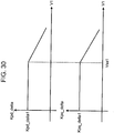
- Fig. 30 is a view showing a condition in which the differential current gains are varied on the basis of the first voltage commands, according to the fourth embodiment of this invention.
- Fig. 30 shows a case in which the differential current gains Kpd_delta, Kpq_delta are varied in accordance with an amplitude V1 of the first voltage commands.
- the differential current gains Kpd_delta, Kpq_delta are set respectively at fixed values Kpd_delta1, Kpq_delta1.
- the differential current gains Kpd_delta, Kpq_delta are reduced along a straight line.
- the threshold Vsa1 and an incline of the straight line may be determined in accordance with a generated pulsation level.
- the abscissa of Fig. 30 may be set as the square of the amplitude.
- an amplitude V2 of the second voltage commands which is given below in Equation (36)
- an amplitude V_sum of the sum voltages which is given below in Equation (37)
- V1, V2, and V_sum may be used as the abscissa of Fig. 30 .
- V_sum 2 V dsum 2 + V qsum 2
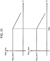
- Fig. 31 is a view showing a condition in which the sum current gains are varied on the basis of the first voltage commands, according to the fourth embodiment of this invention.
- Fig. 31 shows an example of a case in which the sum current gains Kpd_sum, Kpq_sum are varied in accordance with the amplitude V1 of the first voltage commands.
- the sum current gains Kpd_sum, Kpq_sum are set respectively at fixed values Kpd_sum1, Kpq_sum1.
- the sum current gains Kpd_sum, Kpq_sum are reduced along a straight line.
- the threshold Vsal and the incline of the straight line may be determined in accordance with the generated pulsation level.
- the amplitude V2 of the second voltage commands which is given above in Equation (36)
- the amplitude V_sum of the sum voltages which is given above in Equation (37)
- a combination of V1, V2, and V_sum may be used as the abscissa of Fig. 31 .
- the sum current gains Kpd_sum, Kpq_sum may be switched in accordance with effective values rather than the amplitude of the first voltage commands, the second voltage commands, or the sum voltages.
- control device for an AC rotary machine described in the first to fourth embodiments may be applied to control of an electric power steering having a control device for an AC rotary machine.
- An electric power steering device requires a control unit that calculates first voltage commands and second voltage commands such that the AC rotary machine generates torque for assisting the steering torque of a steering system.
- the control device for an AC rotary machine according to this invention as a control unit for an electric power steering device of this type, the first voltage commands and the second voltage commands can be calculated at a high amplitude while maintaining the switching period Tsw.
- a steering system in which the switching frequency, which is given by the inverse of the switching period, is outside the audible range such that increased output is obtained at an identical volume ratio while keeping the amount of noise low can be constructed.
- the device can be reduced in size while obtaining an identical output ratio, and therefore a steering system that is easy to install can be realized.
Landscapes
- Engineering & Computer Science (AREA)
- Power Engineering (AREA)
- Control Of Ac Motors In General (AREA)
Applications Claiming Priority (1)
| Application Number | Priority Date | Filing Date | Title |
|---|---|---|---|
| PCT/JP2015/051502 WO2016117047A1 (ja) | 2015-01-21 | 2015-01-21 | 交流回転機の制御装置および電動パワーステアリングの制御装置 |
Publications (3)
| Publication Number | Publication Date |
|---|---|
| EP3249804A1 true EP3249804A1 (de) | 2017-11-29 |
| EP3249804A4 EP3249804A4 (de) | 2018-08-29 |
| EP3249804B1 EP3249804B1 (de) | 2021-08-04 |
Family
ID=56416613
Family Applications (1)
| Application Number | Title | Priority Date | Filing Date |
|---|---|---|---|
| EP15878742.4A Active EP3249804B1 (de) | 2015-01-21 | 2015-01-21 | Steuerungsvorrichtung für einen wechselstrommotor und steuerungsvorrichtung für eine elektrische servolenkung |
Country Status (5)
| Country | Link |
|---|---|
| US (1) | US9923504B2 (de) |
| EP (1) | EP3249804B1 (de) |
| JP (1) | JP6227173B2 (de) |
| CN (1) | CN107112938B (de) |
| WO (1) | WO2016117047A1 (de) |
Families Citing this family (7)
| Publication number | Priority date | Publication date | Assignee | Title |
|---|---|---|---|---|
| CN109496190B (zh) * | 2016-07-20 | 2020-01-21 | 日本精工株式会社 | 电动助力转向装置 |
| CN109463039B (zh) * | 2016-07-20 | 2020-02-28 | 日本精工株式会社 | 电动助力转向装置 |
| DE102017213069A1 (de) * | 2017-07-28 | 2019-01-31 | Robert Bosch Gmbh | Verfahren zur Bestimmung einer Rotorlage einer elektrischen, rotierenden Maschine sowie eine elektrische, rotierende Maschine zur Durchführung eines solchen Verfahrens |
| US10696175B2 (en) | 2017-08-16 | 2020-06-30 | Ford Global Technologies, Llc | Variable inverter output |
| JP6712096B2 (ja) * | 2017-08-21 | 2020-06-17 | 三菱電機株式会社 | 電力変換装置および電動パワーステアリング装置 |
| JP6958230B2 (ja) * | 2017-10-24 | 2021-11-02 | 株式会社デンソー | 回転電機の制御装置 |
| JP7035684B2 (ja) * | 2018-03-22 | 2022-03-15 | 株式会社デンソー | システム |
Family Cites Families (14)
| Publication number | Priority date | Publication date | Assignee | Title |
|---|---|---|---|---|
| JPH03230767A (ja) | 1990-02-01 | 1991-10-14 | Toshiba Corp | 三相pwmインバータ装置における相電流検出装置 |
| JP3931079B2 (ja) * | 2001-12-14 | 2007-06-13 | 松下電器産業株式会社 | 電動機駆動装置及びそれを用いた冷凍装置 |
| JP4703537B2 (ja) | 2006-10-30 | 2011-06-15 | 三菱電機株式会社 | 3相pwm信号発生装置および3相電圧型インバータ装置 |
| JP4804381B2 (ja) * | 2007-02-28 | 2011-11-02 | 三菱電機株式会社 | 電動機駆動制御装置及び電動機 |
| JP4978429B2 (ja) * | 2007-11-01 | 2012-07-18 | アイシン・エィ・ダブリュ株式会社 | 電動機制御装置,電気自動車およびハイブリッド電気自動車 |
| JP5471259B2 (ja) * | 2009-10-02 | 2014-04-16 | アイシン・エィ・ダブリュ株式会社 | 制御装置 |
| JP5252229B2 (ja) * | 2009-10-02 | 2013-07-31 | アイシン・エィ・ダブリュ株式会社 | 電動機駆動装置の制御装置 |
| JP5402948B2 (ja) * | 2011-01-05 | 2014-01-29 | 日本精工株式会社 | モータ制御装置及びそれを用いた電動パワーステアリング装置 |
| JP2012178927A (ja) * | 2011-02-25 | 2012-09-13 | Sanyo Electric Co Ltd | インバータ制御装置 |
| JP5465269B2 (ja) * | 2012-03-29 | 2014-04-09 | 三菱電機株式会社 | 故障検出回路を備えた電動機駆動装置および電動機駆動装置の故障検出方法 |
| JP5556845B2 (ja) * | 2012-04-26 | 2014-07-23 | 株式会社デンソー | 3相回転機の制御装置 |
| JP5590076B2 (ja) * | 2012-07-04 | 2014-09-17 | 株式会社デンソー | 多相回転機の制御装置 |
| JP5968805B2 (ja) * | 2013-02-28 | 2016-08-10 | 日立オートモティブシステムズ株式会社 | モータ装置およびモータ駆動装置 |
| JP6091646B2 (ja) * | 2013-11-11 | 2017-03-08 | 三菱電機株式会社 | 電力変換装置 |
-
2015
- 2015-01-21 JP JP2016570393A patent/JP6227173B2/ja not_active Expired - Fee Related
- 2015-01-21 EP EP15878742.4A patent/EP3249804B1/de active Active
- 2015-01-21 WO PCT/JP2015/051502 patent/WO2016117047A1/ja not_active Ceased
- 2015-01-21 US US15/524,531 patent/US9923504B2/en active Active
- 2015-01-21 CN CN201580073466.7A patent/CN107112938B/zh not_active Expired - Fee Related
Also Published As
| Publication number | Publication date |
|---|---|
| US9923504B2 (en) | 2018-03-20 |
| CN107112938B (zh) | 2019-06-21 |
| CN107112938A (zh) | 2017-08-29 |
| JP6227173B2 (ja) | 2017-11-08 |
| EP3249804B1 (de) | 2021-08-04 |
| US20170331405A1 (en) | 2017-11-16 |
| EP3249804A4 (de) | 2018-08-29 |
| WO2016117047A1 (ja) | 2016-07-28 |
| JPWO2016117047A1 (ja) | 2017-04-27 |
Similar Documents
| Publication | Publication Date | Title |
|---|---|---|
| EP3110001A1 (de) | Wechselstromdrehmaschinensteuerungsvorrichtung und steuerungsvorrichtung für eine elektrische servolenkung | |
| EP3249804B1 (de) | Steuerungsvorrichtung für einen wechselstrommotor und steuerungsvorrichtung für eine elektrische servolenkung | |
| AU2007353089B2 (en) | Power conversion system | |
| CN101809857B (zh) | 旋转电机的控制装置 | |
| US10199979B2 (en) | Power conversion device | |
| US10666169B2 (en) | Control device for AC rotary machine and control device for electric power steering | |
| US20150137779A1 (en) | Matrix converter and method for controlling matrix converter | |
| EP3477842A1 (de) | Stromwandlungsvorrichtung | |
| EP3651339A1 (de) | Wandlervorrichtung und elektrische servolenkung | |
| CA2714211A1 (en) | Electrical power conversion apparatus | |
| EP3249805B1 (de) | Steuerungsvorrichtung für eine wechselstromdrehmaschine und steuerungsvorrichtung für eine elektrische servolenkung | |
| JP4401724B2 (ja) | 電力変換装置 | |
| CN101471622B (zh) | 换流器的控制装置 | |
| HK1159334B (en) | Power conversion device | |
| HK1144501B (en) | Controller of rotary electric machine |
Legal Events
| Date | Code | Title | Description |
|---|---|---|---|
| STAA | Information on the status of an ep patent application or granted ep patent |
Free format text: STATUS: THE INTERNATIONAL PUBLICATION HAS BEEN MADE |
|
| PUAI | Public reference made under article 153(3) epc to a published international application that has entered the european phase |
Free format text: ORIGINAL CODE: 0009012 |
|
| STAA | Information on the status of an ep patent application or granted ep patent |
Free format text: STATUS: REQUEST FOR EXAMINATION WAS MADE |
|
| 17P | Request for examination filed |
Effective date: 20170601 |
|
| AK | Designated contracting states |
Kind code of ref document: A1 Designated state(s): AL AT BE BG CH CY CZ DE DK EE ES FI FR GB GR HR HU IE IS IT LI LT LU LV MC MK MT NL NO PL PT RO RS SE SI SK SM TR |
|
| AX | Request for extension of the european patent |
Extension state: BA ME |
|
| DAX | Request for extension of the european patent (deleted) | ||
| A4 | Supplementary search report drawn up and despatched |
Effective date: 20180730 |
|
| RIC1 | Information provided on ipc code assigned before grant |
Ipc: H02P 21/22 20160101AFI20180724BHEP Ipc: H02P 25/22 20060101ALI20180724BHEP |
|
| STAA | Information on the status of an ep patent application or granted ep patent |
Free format text: STATUS: EXAMINATION IS IN PROGRESS |
|
| 17Q | First examination report despatched |
Effective date: 20200507 |
|
| REG | Reference to a national code |
Ref country code: DE Ref legal event code: R079 Ref document number: 602015072056 Country of ref document: DE Free format text: PREVIOUS MAIN CLASS: H02P0027060000 Ipc: H02P0021220000 |
|
| GRAP | Despatch of communication of intention to grant a patent |
Free format text: ORIGINAL CODE: EPIDOSNIGR1 |
|
| STAA | Information on the status of an ep patent application or granted ep patent |
Free format text: STATUS: GRANT OF PATENT IS INTENDED |
|
| RIC1 | Information provided on ipc code assigned before grant |
Ipc: H02P 25/22 20060101ALI20200911BHEP Ipc: H02P 21/22 20160101AFI20200911BHEP Ipc: H02P 29/028 20160101ALI20200911BHEP |
|
| INTG | Intention to grant announced |
Effective date: 20200928 |
|
| RIN1 | Information on inventor provided before grant (corrected) |
Inventor name: FURUKAWA, AKIRA Inventor name: MORI, TATSUYA |
|
| GRAJ | Information related to disapproval of communication of intention to grant by the applicant or resumption of examination proceedings by the epo deleted |
Free format text: ORIGINAL CODE: EPIDOSDIGR1 |
|
| STAA | Information on the status of an ep patent application or granted ep patent |
Free format text: STATUS: EXAMINATION IS IN PROGRESS |
|
| GRAP | Despatch of communication of intention to grant a patent |
Free format text: ORIGINAL CODE: EPIDOSNIGR1 |
|
| STAA | Information on the status of an ep patent application or granted ep patent |
Free format text: STATUS: GRANT OF PATENT IS INTENDED |
|
| INTC | Intention to grant announced (deleted) | ||
| GRAJ | Information related to disapproval of communication of intention to grant by the applicant or resumption of examination proceedings by the epo deleted |
Free format text: ORIGINAL CODE: EPIDOSDIGR1 |
|
| STAA | Information on the status of an ep patent application or granted ep patent |
Free format text: STATUS: EXAMINATION IS IN PROGRESS |
|
| INTG | Intention to grant announced |
Effective date: 20210216 |
|
| GRAP | Despatch of communication of intention to grant a patent |
Free format text: ORIGINAL CODE: EPIDOSNIGR1 |
|
| STAA | Information on the status of an ep patent application or granted ep patent |
Free format text: STATUS: GRANT OF PATENT IS INTENDED |
|
| INTC | Intention to grant announced (deleted) | ||
| INTG | Intention to grant announced |
Effective date: 20210407 |
|
| GRAS | Grant fee paid |
Free format text: ORIGINAL CODE: EPIDOSNIGR3 |
|
| GRAA | (expected) grant |
Free format text: ORIGINAL CODE: 0009210 |
|
| STAA | Information on the status of an ep patent application or granted ep patent |
Free format text: STATUS: THE PATENT HAS BEEN GRANTED |
|
| AK | Designated contracting states |
Kind code of ref document: B1 Designated state(s): AL AT BE BG CH CY CZ DE DK EE ES FI FR GB GR HR HU IE IS IT LI LT LU LV MC MK MT NL NO PL PT RO RS SE SI SK SM TR |
|
| REG | Reference to a national code |
Ref country code: GB Ref legal event code: FG4D |
|
| REG | Reference to a national code |
Ref country code: AT Ref legal event code: REF Ref document number: 1418031 Country of ref document: AT Kind code of ref document: T Effective date: 20210815 |
|
| REG | Reference to a national code |
Ref country code: CH Ref legal event code: EP |
|
| REG | Reference to a national code |
Ref country code: DE Ref legal event code: R096 Ref document number: 602015072056 Country of ref document: DE |
|
| REG | Reference to a national code |
Ref country code: IE Ref legal event code: FG4D |
|
| REG | Reference to a national code |
Ref country code: LT Ref legal event code: MG9D |
|
| REG | Reference to a national code |
Ref country code: NL Ref legal event code: MP Effective date: 20210804 |
|
| REG | Reference to a national code |
Ref country code: AT Ref legal event code: MK05 Ref document number: 1418031 Country of ref document: AT Kind code of ref document: T Effective date: 20210804 |
|
| PG25 | Lapsed in a contracting state [announced via postgrant information from national office to epo] |
Ref country code: LT Free format text: LAPSE BECAUSE OF FAILURE TO SUBMIT A TRANSLATION OF THE DESCRIPTION OR TO PAY THE FEE WITHIN THE PRESCRIBED TIME-LIMIT Effective date: 20210804 Ref country code: BG Free format text: LAPSE BECAUSE OF FAILURE TO SUBMIT A TRANSLATION OF THE DESCRIPTION OR TO PAY THE FEE WITHIN THE PRESCRIBED TIME-LIMIT Effective date: 20211104 Ref country code: AT Free format text: LAPSE BECAUSE OF FAILURE TO SUBMIT A TRANSLATION OF THE DESCRIPTION OR TO PAY THE FEE WITHIN THE PRESCRIBED TIME-LIMIT Effective date: 20210804 Ref country code: NO Free format text: LAPSE BECAUSE OF FAILURE TO SUBMIT A TRANSLATION OF THE DESCRIPTION OR TO PAY THE FEE WITHIN THE PRESCRIBED TIME-LIMIT Effective date: 20211104 Ref country code: PT Free format text: LAPSE BECAUSE OF FAILURE TO SUBMIT A TRANSLATION OF THE DESCRIPTION OR TO PAY THE FEE WITHIN THE PRESCRIBED TIME-LIMIT Effective date: 20211206 Ref country code: FI Free format text: LAPSE BECAUSE OF FAILURE TO SUBMIT A TRANSLATION OF THE DESCRIPTION OR TO PAY THE FEE WITHIN THE PRESCRIBED TIME-LIMIT Effective date: 20210804 Ref country code: ES Free format text: LAPSE BECAUSE OF FAILURE TO SUBMIT A TRANSLATION OF THE DESCRIPTION OR TO PAY THE FEE WITHIN THE PRESCRIBED TIME-LIMIT Effective date: 20210804 Ref country code: SE Free format text: LAPSE BECAUSE OF FAILURE TO SUBMIT A TRANSLATION OF THE DESCRIPTION OR TO PAY THE FEE WITHIN THE PRESCRIBED TIME-LIMIT Effective date: 20210804 Ref country code: RS Free format text: LAPSE BECAUSE OF FAILURE TO SUBMIT A TRANSLATION OF THE DESCRIPTION OR TO PAY THE FEE WITHIN THE PRESCRIBED TIME-LIMIT Effective date: 20210804 Ref country code: HR Free format text: LAPSE BECAUSE OF FAILURE TO SUBMIT A TRANSLATION OF THE DESCRIPTION OR TO PAY THE FEE WITHIN THE PRESCRIBED TIME-LIMIT Effective date: 20210804 |
|
| PG25 | Lapsed in a contracting state [announced via postgrant information from national office to epo] |
Ref country code: PL Free format text: LAPSE BECAUSE OF FAILURE TO SUBMIT A TRANSLATION OF THE DESCRIPTION OR TO PAY THE FEE WITHIN THE PRESCRIBED TIME-LIMIT Effective date: 20210804 Ref country code: LV Free format text: LAPSE BECAUSE OF FAILURE TO SUBMIT A TRANSLATION OF THE DESCRIPTION OR TO PAY THE FEE WITHIN THE PRESCRIBED TIME-LIMIT Effective date: 20210804 Ref country code: GR Free format text: LAPSE BECAUSE OF FAILURE TO SUBMIT A TRANSLATION OF THE DESCRIPTION OR TO PAY THE FEE WITHIN THE PRESCRIBED TIME-LIMIT Effective date: 20211105 |
|
| PG25 | Lapsed in a contracting state [announced via postgrant information from national office to epo] |
Ref country code: NL Free format text: LAPSE BECAUSE OF FAILURE TO SUBMIT A TRANSLATION OF THE DESCRIPTION OR TO PAY THE FEE WITHIN THE PRESCRIBED TIME-LIMIT Effective date: 20210804 |
|
| PG25 | Lapsed in a contracting state [announced via postgrant information from national office to epo] |
Ref country code: DK Free format text: LAPSE BECAUSE OF FAILURE TO SUBMIT A TRANSLATION OF THE DESCRIPTION OR TO PAY THE FEE WITHIN THE PRESCRIBED TIME-LIMIT Effective date: 20210804 |
|
| REG | Reference to a national code |
Ref country code: DE Ref legal event code: R097 Ref document number: 602015072056 Country of ref document: DE |
|
| PG25 | Lapsed in a contracting state [announced via postgrant information from national office to epo] |
Ref country code: SM Free format text: LAPSE BECAUSE OF FAILURE TO SUBMIT A TRANSLATION OF THE DESCRIPTION OR TO PAY THE FEE WITHIN THE PRESCRIBED TIME-LIMIT Effective date: 20210804 Ref country code: SK Free format text: LAPSE BECAUSE OF FAILURE TO SUBMIT A TRANSLATION OF THE DESCRIPTION OR TO PAY THE FEE WITHIN THE PRESCRIBED TIME-LIMIT Effective date: 20210804 Ref country code: RO Free format text: LAPSE BECAUSE OF FAILURE TO SUBMIT A TRANSLATION OF THE DESCRIPTION OR TO PAY THE FEE WITHIN THE PRESCRIBED TIME-LIMIT Effective date: 20210804 Ref country code: EE Free format text: LAPSE BECAUSE OF FAILURE TO SUBMIT A TRANSLATION OF THE DESCRIPTION OR TO PAY THE FEE WITHIN THE PRESCRIBED TIME-LIMIT Effective date: 20210804 Ref country code: CZ Free format text: LAPSE BECAUSE OF FAILURE TO SUBMIT A TRANSLATION OF THE DESCRIPTION OR TO PAY THE FEE WITHIN THE PRESCRIBED TIME-LIMIT Effective date: 20210804 Ref country code: AL Free format text: LAPSE BECAUSE OF FAILURE TO SUBMIT A TRANSLATION OF THE DESCRIPTION OR TO PAY THE FEE WITHIN THE PRESCRIBED TIME-LIMIT Effective date: 20210804 |
|
| PLBE | No opposition filed within time limit |
Free format text: ORIGINAL CODE: 0009261 |
|
| STAA | Information on the status of an ep patent application or granted ep patent |
Free format text: STATUS: NO OPPOSITION FILED WITHIN TIME LIMIT |
|
| 26N | No opposition filed |
Effective date: 20220506 |
|
| PG25 | Lapsed in a contracting state [announced via postgrant information from national office to epo] |
Ref country code: IT Free format text: LAPSE BECAUSE OF FAILURE TO SUBMIT A TRANSLATION OF THE DESCRIPTION OR TO PAY THE FEE WITHIN THE PRESCRIBED TIME-LIMIT Effective date: 20210804 |
|
| PG25 | Lapsed in a contracting state [announced via postgrant information from national office to epo] |
Ref country code: SI Free format text: LAPSE BECAUSE OF FAILURE TO SUBMIT A TRANSLATION OF THE DESCRIPTION OR TO PAY THE FEE WITHIN THE PRESCRIBED TIME-LIMIT Effective date: 20210804 Ref country code: MC Free format text: LAPSE BECAUSE OF FAILURE TO SUBMIT A TRANSLATION OF THE DESCRIPTION OR TO PAY THE FEE WITHIN THE PRESCRIBED TIME-LIMIT Effective date: 20210804 |
|
| REG | Reference to a national code |
Ref country code: CH Ref legal event code: PL |
|
| GBPC | Gb: european patent ceased through non-payment of renewal fee |
Effective date: 20220121 |
|
| REG | Reference to a national code |
Ref country code: BE Ref legal event code: MM Effective date: 20220131 |
|
| PG25 | Lapsed in a contracting state [announced via postgrant information from national office to epo] |
Ref country code: LU Free format text: LAPSE BECAUSE OF NON-PAYMENT OF DUE FEES Effective date: 20220121 Ref country code: GB Free format text: LAPSE BECAUSE OF NON-PAYMENT OF DUE FEES Effective date: 20220121 |
|
| PG25 | Lapsed in a contracting state [announced via postgrant information from national office to epo] |
Ref country code: BE Free format text: LAPSE BECAUSE OF NON-PAYMENT OF DUE FEES Effective date: 20220131 |
|
| PG25 | Lapsed in a contracting state [announced via postgrant information from national office to epo] |
Ref country code: LI Free format text: LAPSE BECAUSE OF NON-PAYMENT OF DUE FEES Effective date: 20220131 Ref country code: CH Free format text: LAPSE BECAUSE OF NON-PAYMENT OF DUE FEES Effective date: 20220131 |
|
| PG25 | Lapsed in a contracting state [announced via postgrant information from national office to epo] |
Ref country code: IE Free format text: LAPSE BECAUSE OF NON-PAYMENT OF DUE FEES Effective date: 20220121 |
|
| PGFP | Annual fee paid to national office [announced via postgrant information from national office to epo] |
Ref country code: FR Payment date: 20221208 Year of fee payment: 9 |
|
| PGFP | Annual fee paid to national office [announced via postgrant information from national office to epo] |
Ref country code: DE Payment date: 20221130 Year of fee payment: 9 |
|
| P01 | Opt-out of the competence of the unified patent court (upc) registered |
Effective date: 20230512 |
|
| PG25 | Lapsed in a contracting state [announced via postgrant information from national office to epo] |
Ref country code: HU Free format text: LAPSE BECAUSE OF FAILURE TO SUBMIT A TRANSLATION OF THE DESCRIPTION OR TO PAY THE FEE WITHIN THE PRESCRIBED TIME-LIMIT; INVALID AB INITIO Effective date: 20150121 |
|
| PG25 | Lapsed in a contracting state [announced via postgrant information from national office to epo] |
Ref country code: MK Free format text: LAPSE BECAUSE OF FAILURE TO SUBMIT A TRANSLATION OF THE DESCRIPTION OR TO PAY THE FEE WITHIN THE PRESCRIBED TIME-LIMIT Effective date: 20210804 Ref country code: CY Free format text: LAPSE BECAUSE OF FAILURE TO SUBMIT A TRANSLATION OF THE DESCRIPTION OR TO PAY THE FEE WITHIN THE PRESCRIBED TIME-LIMIT Effective date: 20210804 |
|
| REG | Reference to a national code |
Ref country code: DE Ref legal event code: R119 Ref document number: 602015072056 Country of ref document: DE |
|
| PG25 | Lapsed in a contracting state [announced via postgrant information from national office to epo] |
Ref country code: MT Free format text: LAPSE BECAUSE OF FAILURE TO SUBMIT A TRANSLATION OF THE DESCRIPTION OR TO PAY THE FEE WITHIN THE PRESCRIBED TIME-LIMIT Effective date: 20210804 |
|
| PG25 | Lapsed in a contracting state [announced via postgrant information from national office to epo] |
Ref country code: DE Free format text: LAPSE BECAUSE OF NON-PAYMENT OF DUE FEES Effective date: 20240801 |
|
| PG25 | Lapsed in a contracting state [announced via postgrant information from national office to epo] |
Ref country code: FR Free format text: LAPSE BECAUSE OF NON-PAYMENT OF DUE FEES Effective date: 20240131 |
|
| PG25 | Lapsed in a contracting state [announced via postgrant information from national office to epo] |
Ref country code: FR Free format text: LAPSE BECAUSE OF NON-PAYMENT OF DUE FEES Effective date: 20240131 Ref country code: DE Free format text: LAPSE BECAUSE OF NON-PAYMENT OF DUE FEES Effective date: 20240801 |
|
| PG25 | Lapsed in a contracting state [announced via postgrant information from national office to epo] |
Ref country code: TR Free format text: LAPSE BECAUSE OF FAILURE TO SUBMIT A TRANSLATION OF THE DESCRIPTION OR TO PAY THE FEE WITHIN THE PRESCRIBED TIME-LIMIT Effective date: 20210804 |