EP3236304A1 - Scanspiegelvorrichtung und verfahren zur herstellung davon - Google Patents
Scanspiegelvorrichtung und verfahren zur herstellung davon Download PDFInfo
- Publication number
- EP3236304A1 EP3236304A1 EP17165853.7A EP17165853A EP3236304A1 EP 3236304 A1 EP3236304 A1 EP 3236304A1 EP 17165853 A EP17165853 A EP 17165853A EP 3236304 A1 EP3236304 A1 EP 3236304A1
- Authority
- EP
- European Patent Office
- Prior art keywords
- wafer
- layer
- mirror
- cavity
- glass
- Prior art date
- Legal status (The legal status is an assumption and is not a legal conclusion. Google has not performed a legal analysis and makes no representation as to the accuracy of the status listed.)
- Granted
Links
Images



Classifications
-
- G—PHYSICS
- G02—OPTICS
- G02B—OPTICAL ELEMENTS, SYSTEMS OR APPARATUS
- G02B26/00—Optical devices or arrangements for the control of light using movable or deformable optical elements
- G02B26/08—Optical devices or arrangements for the control of light using movable or deformable optical elements for controlling the direction of light
- G02B26/0816—Optical devices or arrangements for the control of light using movable or deformable optical elements for controlling the direction of light by means of one or more reflecting elements
- G02B26/0833—Optical devices or arrangements for the control of light using movable or deformable optical elements for controlling the direction of light by means of one or more reflecting elements the reflecting element being a micromechanical device, e.g. a MEMS mirror, DMD
- G02B26/085—Optical devices or arrangements for the control of light using movable or deformable optical elements for controlling the direction of light by means of one or more reflecting elements the reflecting element being a micromechanical device, e.g. a MEMS mirror, DMD the reflecting means being moved or deformed by electromagnetic means
-
- B—PERFORMING OPERATIONS; TRANSPORTING
- B81—MICROSTRUCTURAL TECHNOLOGY
- B81B—MICROSTRUCTURAL DEVICES OR SYSTEMS, e.g. MICROMECHANICAL DEVICES
- B81B3/00—Devices comprising flexible or deformable elements, e.g. comprising elastic tongues or membranes
- B81B3/0035—Constitution or structural means for controlling the movement of the flexible or deformable elements
- B81B3/0054—For holding or placing an element in a given position
-
- B—PERFORMING OPERATIONS; TRANSPORTING
- B81—MICROSTRUCTURAL TECHNOLOGY
- B81B—MICROSTRUCTURAL DEVICES OR SYSTEMS, e.g. MICROMECHANICAL DEVICES
- B81B3/00—Devices comprising flexible or deformable elements, e.g. comprising elastic tongues or membranes
- B81B3/0064—Constitution or structural means for improving or controlling the physical properties of a device
- B81B3/0067—Mechanical properties
- B81B3/007—For controlling stiffness, e.g. ribs
-
- B—PERFORMING OPERATIONS; TRANSPORTING
- B81—MICROSTRUCTURAL TECHNOLOGY
- B81B—MICROSTRUCTURAL DEVICES OR SYSTEMS, e.g. MICROMECHANICAL DEVICES
- B81B7/00—Microstructural systems ; Auxiliary parts of microstructural devices or systems
- B81B7/0032—Packages or encapsulation
- B81B7/0067—Packages or encapsulation for controlling the passage of optical signals through the package
-
- B—PERFORMING OPERATIONS; TRANSPORTING
- B81—MICROSTRUCTURAL TECHNOLOGY
- B81C—PROCESSES OR APPARATUS SPECIALLY ADAPTED FOR THE MANUFACTURE OR TREATMENT OF MICROSTRUCTURAL DEVICES OR SYSTEMS
- B81C1/00—Manufacture or treatment of devices or systems in or on a substrate
- B81C1/00015—Manufacture or treatment of devices or systems in or on a substrate for manufacturing microsystems
- B81C1/00134—Manufacture or treatment of devices or systems in or on a substrate for manufacturing microsystems comprising flexible or deformable structures
- B81C1/0019—Flexible or deformable structures not provided for in groups B81C1/00142 - B81C1/00182
-
- G—PHYSICS
- G02—OPTICS
- G02B—OPTICAL ELEMENTS, SYSTEMS OR APPARATUS
- G02B1/00—Optical elements characterised by the material of which they are made; Optical coatings for optical elements
- G02B1/10—Optical coatings produced by application to, or surface treatment of, optical elements
- G02B1/11—Anti-reflection coatings
-
- G—PHYSICS
- G02—OPTICS
- G02B—OPTICAL ELEMENTS, SYSTEMS OR APPARATUS
- G02B26/00—Optical devices or arrangements for the control of light using movable or deformable optical elements
- G02B26/08—Optical devices or arrangements for the control of light using movable or deformable optical elements for controlling the direction of light
- G02B26/0816—Optical devices or arrangements for the control of light using movable or deformable optical elements for controlling the direction of light by means of one or more reflecting elements
- G02B26/0833—Optical devices or arrangements for the control of light using movable or deformable optical elements for controlling the direction of light by means of one or more reflecting elements the reflecting element being a micromechanical device, e.g. a MEMS mirror, DMD
-
- G—PHYSICS
- G02—OPTICS
- G02B—OPTICAL ELEMENTS, SYSTEMS OR APPARATUS
- G02B26/00—Optical devices or arrangements for the control of light using movable or deformable optical elements
- G02B26/08—Optical devices or arrangements for the control of light using movable or deformable optical elements for controlling the direction of light
- G02B26/0816—Optical devices or arrangements for the control of light using movable or deformable optical elements for controlling the direction of light by means of one or more reflecting elements
- G02B26/0833—Optical devices or arrangements for the control of light using movable or deformable optical elements for controlling the direction of light by means of one or more reflecting elements the reflecting element being a micromechanical device, e.g. a MEMS mirror, DMD
- G02B26/0841—Optical devices or arrangements for the control of light using movable or deformable optical elements for controlling the direction of light by means of one or more reflecting elements the reflecting element being a micromechanical device, e.g. a MEMS mirror, DMD the reflecting element being moved or deformed by electrostatic means
-
- G—PHYSICS
- G02—OPTICS
- G02B—OPTICAL ELEMENTS, SYSTEMS OR APPARATUS
- G02B26/00—Optical devices or arrangements for the control of light using movable or deformable optical elements
- G02B26/08—Optical devices or arrangements for the control of light using movable or deformable optical elements for controlling the direction of light
- G02B26/0816—Optical devices or arrangements for the control of light using movable or deformable optical elements for controlling the direction of light by means of one or more reflecting elements
- G02B26/0833—Optical devices or arrangements for the control of light using movable or deformable optical elements for controlling the direction of light by means of one or more reflecting elements the reflecting element being a micromechanical device, e.g. a MEMS mirror, DMD
- G02B26/0858—Optical devices or arrangements for the control of light using movable or deformable optical elements for controlling the direction of light by means of one or more reflecting elements the reflecting element being a micromechanical device, e.g. a MEMS mirror, DMD the reflecting means being moved or deformed by piezoelectric means
-
- G—PHYSICS
- G02—OPTICS
- G02B—OPTICAL ELEMENTS, SYSTEMS OR APPARATUS
- G02B26/00—Optical devices or arrangements for the control of light using movable or deformable optical elements
- G02B26/08—Optical devices or arrangements for the control of light using movable or deformable optical elements for controlling the direction of light
- G02B26/10—Scanning systems
-
- G—PHYSICS
- G02—OPTICS
- G02B—OPTICAL ELEMENTS, SYSTEMS OR APPARATUS
- G02B26/00—Optical devices or arrangements for the control of light using movable or deformable optical elements
- G02B26/08—Optical devices or arrangements for the control of light using movable or deformable optical elements for controlling the direction of light
- G02B26/10—Scanning systems
- G02B26/105—Scanning systems with one or more pivoting mirrors or galvano-mirrors
-
- G—PHYSICS
- G02—OPTICS
- G02B—OPTICAL ELEMENTS, SYSTEMS OR APPARATUS
- G02B5/00—Optical elements other than lenses
- G02B5/08—Mirrors
- G02B5/0816—Multilayer mirrors, i.e. having two or more reflecting layers
- G02B5/0825—Multilayer mirrors, i.e. having two or more reflecting layers the reflecting layers comprising dielectric materials only
-
- G—PHYSICS
- G02—OPTICS
- G02B—OPTICAL ELEMENTS, SYSTEMS OR APPARATUS
- G02B7/00—Mountings, adjusting means, or light-tight connections, for optical elements
- G02B7/18—Mountings, adjusting means, or light-tight connections, for optical elements for prisms; for mirrors
- G02B7/182—Mountings, adjusting means, or light-tight connections, for optical elements for prisms; for mirrors for mirrors
- G02B7/1821—Mountings, adjusting means, or light-tight connections, for optical elements for prisms; for mirrors for mirrors for rotating or oscillating mirrors
-
- B—PERFORMING OPERATIONS; TRANSPORTING
- B81—MICROSTRUCTURAL TECHNOLOGY
- B81B—MICROSTRUCTURAL DEVICES OR SYSTEMS, e.g. MICROMECHANICAL DEVICES
- B81B2201/00—Specific applications of microelectromechanical systems
- B81B2201/04—Optical MEMS
- B81B2201/042—Micromirrors, not used as optical switches
-
- B—PERFORMING OPERATIONS; TRANSPORTING
- B81—MICROSTRUCTURAL TECHNOLOGY
- B81B—MICROSTRUCTURAL DEVICES OR SYSTEMS, e.g. MICROMECHANICAL DEVICES
- B81B2203/00—Basic microelectromechanical structures
- B81B2203/01—Suspended structures, i.e. structures allowing a movement
- B81B2203/0109—Bridges
-
- B—PERFORMING OPERATIONS; TRANSPORTING
- B81—MICROSTRUCTURAL TECHNOLOGY
- B81B—MICROSTRUCTURAL DEVICES OR SYSTEMS, e.g. MICROMECHANICAL DEVICES
- B81B2203/00—Basic microelectromechanical structures
- B81B2203/01—Suspended structures, i.e. structures allowing a movement
- B81B2203/0145—Flexible holders
- B81B2203/0163—Spring holders
-
- B—PERFORMING OPERATIONS; TRANSPORTING
- B81—MICROSTRUCTURAL TECHNOLOGY
- B81B—MICROSTRUCTURAL DEVICES OR SYSTEMS, e.g. MICROMECHANICAL DEVICES
- B81B2207/00—Microstructural systems or auxiliary parts thereof
- B81B2207/07—Interconnects
-
- B—PERFORMING OPERATIONS; TRANSPORTING
- B81—MICROSTRUCTURAL TECHNOLOGY
- B81B—MICROSTRUCTURAL DEVICES OR SYSTEMS, e.g. MICROMECHANICAL DEVICES
- B81B2207/00—Microstructural systems or auxiliary parts thereof
- B81B2207/09—Packages
- B81B2207/091—Arrangements for connecting external electrical signals to mechanical structures inside the package
- B81B2207/094—Feed-through, via
- B81B2207/095—Feed-through, via through the lid
-
- B—PERFORMING OPERATIONS; TRANSPORTING
- B81—MICROSTRUCTURAL TECHNOLOGY
- B81C—PROCESSES OR APPARATUS SPECIALLY ADAPTED FOR THE MANUFACTURE OR TREATMENT OF MICROSTRUCTURAL DEVICES OR SYSTEMS
- B81C2203/00—Forming microstructural systems
- B81C2203/01—Packaging MEMS
- B81C2203/0109—Bonding an individual cap on the substrate
-
- G—PHYSICS
- G02—OPTICS
- G02B—OPTICAL ELEMENTS, SYSTEMS OR APPARATUS
- G02B26/00—Optical devices or arrangements for the control of light using movable or deformable optical elements
- G02B26/08—Optical devices or arrangements for the control of light using movable or deformable optical elements for controlling the direction of light
- G02B26/0816—Optical devices or arrangements for the control of light using movable or deformable optical elements for controlling the direction of light by means of one or more reflecting elements
Definitions
- the present invention relates to optical devices, and specifically to scanning mirror structures manufactured with MEMS technologies.
- a scanning mirror can direct a light beam over a range of directions in one or two dimensions, and it may also be used to collect light from a range of directions with good angular accuracy and resolution. Scanning operation over an angular range is obtained by tilting the mirror to an angle and varying this angle as a function of time. Often this varied tilting is done in a periodical or oscillating manner.
- code scanners scanning displays
- laser ranging and imaging sensors Lidars
- a MEMS mirror typically includes a silicon plate with a reflective coating on its top surface, silicon beams for suspension, and actuating structures for one- or two-axis tilting motion of the reflecting silicon plate.
- piezoelectric and electrostatic actuation has been used in the known applications. In either of these methods, achieved forces tend to be too small to generate appropriate deflection amplitudes by direct application of the actuation voltage. Consequently, desired high tilting angles require operation in a resonance mode.
- the resonance mode operation requires low ambient pressure to minimize gas damping, which means that the mirror needs to be hermetically packaged in a low pressure. Hermetic capping is also important because it eliminates corrosion of reflective surfaces of the mirror.
- Wafer-level packaging is presently preferred for MEMS devices in terms of cost, size and manufacturability. It is widely used in mass production of resonating MEMS devices, like gyroscopes and timing resonators.
- MEMS mirrors pose some special requirements for the wafer-level packaging: the element protecting the mirror must provide good optical properties and the package needs to provide enough room for vertical play of the tilting motion of the mirror.
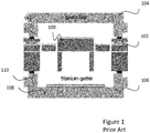
- Figure 1 shows a conventional wafer-level packaged MEMS mirror element, described in document " Resonant biaxial 7-mm MEMS mirror for omnidirectional scanning, Journal of Micro/Nanolitograhy, MEMS and MOEMS, Jan-Mar 2014/Vol. 13(1 ).
- a movable mirror element 100 and elements for actuating it may be formed of a SOI wafer 102 by etching the front side and backside of the SOI wafer.
- the SOI wafer may then be glass frit bonded to side walls of glass cap wafers 104, 106.
- Glass cap wafers 104, 106 shown in Figure 1 are straightforward solutions for hermetic closing of a MEMS mirror package.
- the planar or flat part 108 of the glass cap needs also the spacer part 110 to provide room for the required vertical play of the mirror element. In practice, the required spacing distance may be up to several hundreds of micrometers.
- the spacer part 110 is conventionally formed of a spacer wafer bonded to a flat glass wafer that provides the optical window.
- This increases cost and complexity of the wafer encapsulation since more than one bonding interface needs to be formed and potentially more than one bonding technique must be used.
- a flat glass wafer could be anodically bonded with a silicon spacer wafer, but the silicon spacer wafer would need some other technique for bonding with the silicon wafer of the SOI wafer.
- the spacer part 110 may be formed by etching a cavity into a flat glass cap wafer.
- the optical quality of such glass cap would not be sufficient. It is well known that it is very difficult to produce a surface that is appropriately smooth for optical applications by etching to the bottom of a cavity. Typically etched glass surfaces are rough and non-planar, which causes optical losses by scattering and unwanted refraction of light.
- the solution shown in Figure 1 is avoids optical losses by shaping the desired profile and cavities by softening the glass cap wafer in high temperature. This may be a feasible solution from the wafer bonding point of view, but manufacture of such shaped glass is a relatively complex and expensive process. It includes bonding of glass first into a sacrificial silicon wafer and etching off the sacrificial silicon wafer after the thermal shaping. The total number of wafers needed for the process is therefore the same as with an additional spacer wafer, which means that also no saving in material cost is achieved. There is also a risk that the high temperatures used for glass softening cause crystallization in the glass, and thereby degradation of the optical properties.
- the object of the present invention is to provide a device that is easy to manufacture and still provides excellent optical capping for a scanning mirror. This and other objects of the present invention are achieved with an optical device and a method for manufacturing an optical device according to the independent claims.
- Embodiments of the invention include an optical device that includes a movable mirror part.
- the optical device comprises a glass wafer with a first planar surface in at least one side of the glass wafer; a mirror wafer that comprises a package of a first layer of electrically conductive material, a second layer of electrically conductive material, and a third layer of electrically insulating material between the first layer and the second layer, wherein the first layer has a first side that faces away from the third layer, and the second layer has a second side against the third layer; a suspension spring structure for suspending the movable mirror part, wherein the movable mirror part and the suspension spring structure are fabricated of the second layer of the mirror wafer; a second cavity that extends through at least the first layer of the mirror wafer, wherein the second cavity is circumscribed in the first side by a second planar surface; a reflecting layer carried by the mirror part in the bottom of the second cavity; a cap wafer that has a third side and a fourth side, and includes a
- the cap wafer is bonded to the mirror wafer such that the third side faces away from mirror wafer, and the fourth side is against the second layer of the mirror wafer.
- the glass wafer is bonded to the mirror wafer such that the first planar surface of the glass wafer extends as a plane over the second cavity and in bonded abutment with the second planar surface.
- a hermetically closed space that encloses the movable mirror part thus extends between the first planar surface of the glass wafer and a bottom of the first cavity in the cap wafer.
- Embodiments of the invention include also a method for manufacturing an optical device from a mirror wafer, a cap wafer, and a glass wafer.
- the mirror wafer is a layer package that includes a first layer of electrically conductive material, a second layer of electrically conductive material, and a third layer of electrically insulating material between the first layer and the second layer, wherein the first layer has a first side that faces away from the third layer and the second layer has a second side against the third layer; the cap wafer has a third side and a fourth side opposite each other; and the glass wafer has a first planar surface in at least one side of the glass wafer.
- the method includes fabricating into the cap wafer a first cavity extending from the fourth side into the cap wafer; fabricating through the first layer of the mirror wafer a second cavity that is circumscribed in the first side by a second planar surface; fabricating to the second layer of the mirror wafer a movable mirror part and a suspension spring structure, the mirror part having a reflecting layer in the second side of the second layer; fabricating to the second layer of the mirror wafer an electrical actuation element and wiring for connecting the electrical actuation element to a conductive connection, the electrical actuation element being configured to actuate the movable mirror part in response to electrical signals received through the conductive connection; bonding the cap wafer to the mirror wafer such that the fourth side faces the second layer, and the glass wafer to the mirror wafer such that the first planar surface of the glass wafer extends as a plane over the second cavity and in bonded abutment with the second planar surface, whereby a hermetically closed space that encloses the movable mirror part and extends
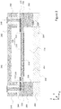
- Figure 2 shows a cross section of a device structure that illustrates an embodiment of an optical device that includes a bonded package of a mirror wafer 200, a cap wafer 240, and a glass wafer 260.
- the mirror wafer 200 comprises a package of a first layer 202 of electrically conductive material, a second layer 204 of electrically conductive material, and a third layer 206 of electrically insulating material between the first layer and the second layer.
- the mirror wafer may be manufactured from layered solid structures, like silicon-on-insulator (SOI) wafers.
- SOI-wafer typically comprises a handle wafer layer, a buried oxide (BOX) layer, and a device wafer layer.
- the handle wafer layer is usually the thickest part, some hundreds of micron thick, while the device layer wafer is typically tens of microns thick.
- the BOX layer is typically from fraction of a micron to a few microns thick.
- the BOX layer may be deposited either on the handle wafer layer, or the device wafer layer, and the two pieces of silicon may be bonded to each other so that the BOX layer is in between them and isolates the device wafer layer electrically from the handle wafer layer.
- Structures with electromechanical properties are typically manufactured into the device layer of a SOI wafer by etching trenches into and/or through the device layer.
- Piezoelectric thin films may be deposited and patterned onto the device layer for actuation and sensing of motions of the structures. Sacrificial etching of the BOX layer can be used to mechanically release selected MEMS structures also from the BOX layer.
- a mirror element 208 that includes a movable mirror part 210 and a suspension spring structure 212 may be fabricated of the second layer 204 of the mirror wafer.
- the suspension spring structure 212 may be etched out of the material of the second layer and have a form that provides a required combination of rigidity and elasticity to operate as a spring upon motions of the mirror part.
- the suspension spring structure 212 may thus couple the mirror part 210 to static parts of the second layer 204 that are bonded to the other layers of the mirror wafer, but allow the mirror part to move in a controlled manner in respect of those static parts.
- the mirror part 210 may also be etched out of the material of the second layer.
- the mirror part 210 may carry a reflecting layer 214.
- the term carry means herein that the reflecting layer 214 is part of, or is mechanically integrated or fixed to the mirror part, and therefore moves with and along motions of the mirror part.
- the first layer 202 has a first side 216 that faces away from the third layer 206
- the second layer 204 has a second side 218 against the third layer 206.
- the reflecting layer 214 is on a surface of the second layer 204, in the second side 218 of the second layer 204 of the mirror wafer 200.
- the mirror part 210 and the suspension spring structure 212 are released also from the third layer 206 by etching.
- An electrical actuation element 220 may be coupled to the mirror element 208 and include an electromechanical transducer that transforms electrical energy into mechanical energy (motion) of the mirror part 210.
- the electrical actuation element may be connected to an electrical energy source, and actuate the mirror part in response to electrical signals received through a conductive connection from the electrical energy source.
- the electrical actuation element may apply capacitive or electrostatic transduction, or piezoelectric transduction.
- piezoelectric elements that controllably actuate the motions of the mirror are shown. Piezoelectric elements may be formed by depositing and patterning one or more layers of piezoelectric materials on the second layer, to the other side of the second layer, opposite the side of the reflective layer 214 of the mirror part 210.
- the electrical actuation element 220 may be coupled to the electrical energy source with wiring 222 that may be fabricated into or onto the structures of the mirror wafer.
- the wiring 222 may be accessed for electrical connection from some side of the mirror wafer.
- the wiring 222 is fabricated on the second layer, in a side that is opposite the second side 218 of the mirror wafer.
- the wiring 222 is therefore accessible for connection through conductive structures of the overlying cap wafer 240.
- the conductive connection may, however, be brought to the wiring 222 in other ways.
- the cap wafer may be smaller than the mirror wafer, and the conductive connection may be brought to the wiring 222 through lateral contacts that run on surfaces of the mirror wafer, which surfaces are not covered by the cap wafer.
- the cap wafer 240 may be bonded to the mirror wafer 200. Let us define that the cap wafer 240 and has a third side 242 that faces away from mirror wafer 200, and a fourth side 244 that becomes bonded against the second layer 204 of the mirror wafer 200. Let us also define that planar sides of wafers are considered to extend along horizontal directions, denoted with X and Y in Figure 2 , and a direction orthogonal to them is a vertical direction, denoted with Z in Figure 2 .
- the cap wafer 240 may include a first cavity 246 that extends from the fourth side 244 of the cap wafer into the cap wafer.
- the first cavity 246 may be dimensioned to form into the cap wafer a space that enables displacements of the mirror element in a vertical direction during its scanning motion.
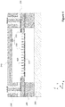
- Figure 3 shows the structure of Figure 2 in a state where the mirror part 210 is in a tilted position during a scanning cycle.
- the cap wafer 240 may also include an electrical contact element 248 accessible from the third side 242 of the cap wafer, and a conductive lead 250 extending through the cap wafer.
- the conductive lead 250 may be a conductive via, formed of a silicon material of the cap wafer, and insulated with surrounding glass filling. However, other types of conductive leads may be applied within the scope.
- the conductive lead 250 may begin from the electrical contact element 248 in the third side, and be accessible for the wiring 222 of the mirror wafer from the fourth side 244 of the cap wafer.
- the conductive lead 250 is positioned in relationship with the wiring 222 of the mirror wafer such that when the cap wafer and the mirror wafer are bonded together, the electrical actuation element 220 becomes electrically connected to the conductive lead 250 of the cap wafer. Due to this, the electrical actuation element 220 is able to actuate the movable mirror part 210 in response to electrical signals received through the electrical contact element 248 in the externally accessible third side 242 of the cap wafer 240.
- the suspension spring structure 212 may include structured silicon beam springs, where one end of each spring is coupled to the rigid, bonded part of the mirror wafer, and the other end of each spring is coupled to the mirror part 210.
- the suspension spring structure may include curved form beams applied in the referred prior art document of Figure 1 .
- springs of a suspension spring structure may be formed of a combination of one or more linear or curved beams coupled together to enable the desired scanning motion.
- a variety of spring forms may be applied within the scope, as long as a controlled elastic suspension between the rigid parts of the mirror wafer and the mirror part is enabled.
- the mirror wafer 200 may include a second cavity 224 that extends through the first layer 202 of the mirror wafer.
- the reflective layer 214 may thus be formed of a metal reflector layer or stack, deposited into the bottom of the second cavity, on the mirror part 210 that is exposed and thus accessible through the second cavity 224.
- the reflective layer 214 may be formed on the mirror part 210 after the third layer 206 is removed to release the moving and suspending parts in the second layer, but before the glass wafer 260 and the mirror wafer 200 are bonded together, as shown in the exemplary embodiment of Figure 2 .
- the reflective layer 214 may alternatively be formed on the third layer 206, but anyway before the glass wafer 260 and the mirror wafer 200 are bonded together, as shown in the exemplary embodiment of Figure 2 .
- the glass wafer 260 may be bonded against the first layer 202 of the mirror wafer 200.
- alkaline containing glasses can be bonded to silicon easily by anodic bonding.
- well known glass-frit or metal bonding techniques are available.
- the glass wafer 260 may be a planar element, which means that it may have a first planar surface 262 in at least one side of the glass wafer.
- a variety of glass materials are transparent in a wide wavelength area, and enable provision of finished high optical quality planar surfaces.
- the second cavity 224 may be circumscribed, or in other words surrounded, in the first side 214 of the first layer by a second planar surface 226.
- the glass wafer 260 may be bonded with the mirror wafer 200 such that the first planar surface 262 of the glass wafer 260 is set against the second planar surface 226 of the first layer 202 of the mirror wafer 200.
- the first planar surface 262 of the glass wafer thereby extends as a plane over the second cavity 224 and continues extending along the same plane in bonded abutment with the second planar surface 226 of the mirror wafer 200.
- a hermetically closed space that encloses the movable mirror part 210, and extends vertically between the first planar surface 262 of the glass wafer and a bottom of the first cavity 246 in the cap wafer is formed.
- the first planar surface 262 forms the inner surface of the optical window, and thus partially defines the quality of the optical window 264 for the operation of the scanning mirror part 210.
- the inner surface of the optical window may be formed of the high-quality finished surface of a pre-processed glass wafer. No complex processing stages for creating the spacing for the vertical play of the mirror part in the optical window side are needed, and excellent optical quality for the optical window is very easily achieved.
- the other side of the glass wafer 260 i.e. the outer side 266 of the glass wafer is a finished planar surface with high optical quality, or at least includes such planar surface in parts that form the optical window 264 for the mirror element 208.
- Thin-film anti-reflective optical coatings can be further deposited to the outer side of the glass wafer to further minimize optical losses in the optical window 264.
- Thin-film anti-reflective coatings can be also deposited to the inner side 262 of the glass wafer before bonding. In such case the coating needs to be removed from the bonding interface 226 before bonding using lithography and etching techniques generally known to a person skilled in the art.
- Figure 4 illustrates a further embodiment of the structure shown in Figures 2 and 3 .
- a backside of the mirror part 210 includes a plurality of indentations 420.
- the backside of the mirror part is herein the side of the second layer 204 of the mirror wafer opposite the reflective layer.
- the backside of the mirror part is thus opposite the second side 218 of the second layer, and faces the first cavity 246 of the cap wafer 240.
- the one or more indentations 420 may be etched, for example as recess etching, into the second layer 204 before the mirror wafer 200 and the cap wafer 240 are bonded together. Other forms of indentations may be applied, as well.
- the inertial forces tend to bend the mirror part.
- a mirror part is conventionally quite thick, or a thinner mirror part is reinforced with additional thick structures.
- the indentations reduce the inertial mass of the mirror part, and the regions of the second layer embracing the indentations 420 reinforce the structure. Sensitivity of the mirror part 210 for bending due to inertial forces is thus improved.
- the reflective surface on the mirror part 210 in Figures 2 , 3 and 4 requires deposition and patterning of reflective metallic or dielectric thin film stacks into a bottom of a relatively deep second cavity. Depths applied in practice may be of the order of 650 micrometers, which require using special patterning techniques developed for MEMS manufacturing. Such techniques include spray coating and ink-jetting of photoresists. They are commercially available but not widely used yet.
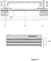
- Figure 5 illustrates a further embodiment where such special processes are not needed, because the reflecting layer is included into the third layer of the mirror wafer at the time of manufacturing the mirror wafer.
- the reflective layer 214 may be formed of a stack of dielectric films that are deposited on the first layer wafer or on the second layer wafer of the mirror wafer before their bonding process, or as part of their bonding process.
- the reflective layer 214 may include a stack of dielectric films that have different values of the refractive index n: Low n (n L ) and High n (n H ).
- n L Low n
- n H High n
- High n materials of the reflective stack may include, for example, Ta2O5 (Tantalum pentoxide), TiO2 (Titanium dioxide), Nb2O5 (Niobium pentoxide), and LaTiO3 (Lanthanum Titanate).
- Low n materials of the reflective stack may include, for example silicon dioxide (SiO2). Also amorphous silicon is sometimes used as a High n material.
- the reflective layer may be formed during fusion bonding process of a handle wafer and a device layer wafer of a SOI wafer. Since the annealing temperature used in the fusion bonding can be as high as 1100 - 1200°C, it is advantageous to select the dielectric materials so that their melting temperatures are above this temperature. Melting points of some commonly used materials are 1,872 °C for Ta2O5, 1,843 °C for TiO2, 1,512 °C for Nb2O5 and > 2000°C LaTiO3, and 1,713 °C SiO2.
- the Low n material is SiO2 and the High n material is Ta2O5.
- the dielectric stack is to select film thicknesses so that the geometrical thickness d of each film in the stack has the value ⁇ /4n where ⁇ is the wavelength of the light and n is the refractive index of the film.
- the number film layers may be increased until the desired value of reflectivity is reached, for example 5-10 High n/Low n pairs.
- Figures 6 and 7 illustrate an example of use of the dielectric stack of Figure 5 in the configurations of Figures 2 and 3 .
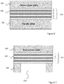
- Figure 6 shows the described mirror wafer 200 with the first layer (handle wafer of a SOI wafer) 202, the second layer (the device layer wafer of the SOI wafer) 204 and the third layer 206, now formed of the layer of dielectric films between the first layer and the second layer wafers 202, 204.
- the dielectric stack forms the reflective layer 214 that may now be exposed by etching the second cavity 224 through the first layer, as shown in Figure 7 .
- the third layer 206 may thus remain on the mirror part, only parts of it need to be etched to release the moving and elastic parts of the mirror element from the second layer 204 and the third layer 206.
- the non-etched part of the third layer will form the reflective layer 214 that is carried on the mirror part of the second layer 204.
- the High n material Ta2O5 would be arranged to the top layer, i.e. to the direction of the incoming laser light.
- TaO5 film reflectivity tends to degrade due to oxygen depletion under the vacuum.
- a very thin (1nm) passivation layer of SiO2 may be arranged to the top layer of the reflective layer to maintain the quality of the Ta2O5 film mirror coating.
- Figures 9-1 to 9-3 illustrate an embodiment of a method for manufacturing an optical device.
- Figure 9-1 illustrates the main steps of the method.
- the two first steps 9-11 and 9-12 are basically independent of each other so their order may be changed, or they may be performed in parallel. Further details for the description of the method steps may be referred from description of Figures 2 to 8 .
- structures of a mirror wafer MW are manufactured (step 9-11).
- the mirror wafer MW may be a layer package that includes a first layer of electrically conductive material, a second layer of electrically conductive material, and a third layer of electrically insulating material between the first layer and the second layer.
- the first layer may have a first side that faces away from the third layer and the second layer may have a second side against the third layer.
- a ready-made SOI wafer may be applied in the step, or a wafer package including a dielectric stack disclosed with Figures 5 to 8 may be manufactured for the purpose.
- a second cavity 2 nd CAV may be fabricated by etching through the first layer of the mirror wafer (step 9-111).
- the second cavity may be etched to a planar surface of a wafer so that it is circumscribed a planar surface, earlier referred to as the second planar surface.
- a mirror element ME including a movable mirror part and a suspension spring structure may be fabricated (step 9-112) to the second layer of the mirror wafer.
- the mirror part may be arranged to have a reflecting layer in the second side of the second layer.
- the third layer may be removed by etching via the second cavity, and the reflecting layer deposited on the second layer through the second cavity.
- the reflecting layer may be deposited on the third layer.
- the third layer may be, or include the reflecting layer that becomes exposed in fabrication of the second cavity.
- an electrical actuation element EA To the second layer of the mirror wafer may be fabricated (step 9-113) an electrical actuation element EA. Also wiring WR for connecting the electrical actuation element to an external actuation energy source may be fabricated (step 9-114) to the second layer of the mirror wafer.
- the electrical actuation element may be configured to actuate the movable mirror part in response to electrical signals received from the external actuation energy source.
- steps 9-12 are also manufactured (step 9-12).
- the cap wafer has a third side and a fourth side opposite each other.
- Main steps of the step 9-12 are described in more detail with Figure 9-3 .
- the method steps illustrate stages of the method in a generic order, which may vary, depending on the applied manufacturing processes.
- a conductive lead CC that extends through the cap wafer may be fabricated (step 9-211) to the cap wafer.
- the conductive lead may be formed, for example, by removing material by etching around a longitudinal via structure to a depth, and filling the surrounding space with glass material.
- the via structure may then be exposed by thinning the cap wafer from the opposite side.
- alternative methods not requiring through layer leads may be applied within the scope.
- An electrical contact element CE accessible from the third side may also be fabricated (step 9-212) into the cap wafer.
- the electrical contact element may be, for example, deposited by patterning a structure of conductive material onto a surface in the third side of the cap wafer. Further, a first cavity 1 st CAV extending from the fourth side into the cap wafer may be fabricated by etching into the cap wafer (step 9-213).
- the glass wafer has a first planar surface in at least one side of the glass wafer.
- the cap wafer, the mirror wafer and a glass wafer may bonded (step 9-13).
- the cap wafer may be bonded to the mirror wafer such that the fourth side faces the second layer, and the glass wafer to the mirror wafer such that the first planar surface of the glass wafer extends as a plane over the second cavity and is in bonded abutment with the second planar surface.
- the wafers may be bonded in separate bonding process stages or in one bonding process stage.
- a hermetically closed space that encloses the movable mirror part and extends between the first planar surface of the glass wafer and a bottom of the first cavity in the cap wafer is thereby formed.
Landscapes
- Physics & Mathematics (AREA)
- Engineering & Computer Science (AREA)
- General Physics & Mathematics (AREA)
- Optics & Photonics (AREA)
- Microelectronics & Electronic Packaging (AREA)
- Computer Hardware Design (AREA)
- Manufacturing & Machinery (AREA)
- Mechanical Engineering (AREA)
- Electromagnetism (AREA)
- Micromachines (AREA)
- Mechanical Light Control Or Optical Switches (AREA)
- Mechanical Optical Scanning Systems (AREA)
- Optical Elements Other Than Lenses (AREA)
Applications Claiming Priority (1)
| Application Number | Priority Date | Filing Date | Title |
|---|---|---|---|
| FI20165337 | 2016-04-18 |
Publications (2)
| Publication Number | Publication Date |
|---|---|
| EP3236304A1 true EP3236304A1 (de) | 2017-10-25 |
| EP3236304B1 EP3236304B1 (de) | 2021-06-16 |
Family
ID=58536828
Family Applications (1)
| Application Number | Title | Priority Date | Filing Date |
|---|---|---|---|
| EP17165853.7A Active EP3236304B1 (de) | 2016-04-18 | 2017-04-11 | Scanspiegelvorrichtung und verfahren zur herstellung davon |
Country Status (5)
| Country | Link |
|---|---|
| US (1) | US10377625B2 (de) |
| EP (1) | EP3236304B1 (de) |
| JP (1) | JP6465145B2 (de) |
| CN (1) | CN107305288B (de) |
| TW (1) | TWI638419B (de) |
Families Citing this family (17)
| Publication number | Priority date | Publication date | Assignee | Title |
|---|---|---|---|---|
| DE102016221038A1 (de) | 2016-10-26 | 2018-04-26 | Robert Bosch Gmbh | Verfahren zur Herstellung eines Schutzwafers mit schräggestellten optischen Fenstern und Vorrichtung |
| WO2019009402A1 (ja) | 2017-07-06 | 2019-01-10 | 浜松ホトニクス株式会社 | 光学デバイス |
| CN108152801B (zh) * | 2017-11-10 | 2022-01-11 | 无锡英菲感知技术有限公司 | 一种动态形变可控微镜 |
| JP6825612B2 (ja) * | 2017-11-13 | 2021-02-03 | 株式会社村田製作所 | 中央支持部を備えたmems反射器 |
| WO2020142088A1 (en) * | 2018-12-31 | 2020-07-09 | Didi Research America, Llc | Micromachined mirror assembly having reflective layers on both sides |
| EP3705451B1 (de) | 2019-03-06 | 2026-04-29 | Murata Manufacturing Co., Ltd. | Mems-struktur mit einer kappe mit einer durchkontaktierung |
| US11662435B2 (en) * | 2019-04-04 | 2023-05-30 | Liturex (Guangzhou) Co. Ltd | Chip scale integrated scanning LiDAR sensor |
| DE102019208373A1 (de) | 2019-06-07 | 2020-12-10 | Infineon Technologies Ag | Herstellen eines MEMS-Bauelements mit Glasabdeckung und MEMS-Bauelement |
| JP7104680B2 (ja) * | 2019-10-10 | 2022-07-21 | 株式会社鷺宮製作所 | Mems素子および振動発電デバイス |
| US11365115B2 (en) * | 2019-09-03 | 2022-06-21 | Taiwan Semiconductor Manufacturing Company, Ltd. | Piezoelectric anti-stiction structure for microelectromechanical systems |
| CN110606464B (zh) * | 2019-09-20 | 2022-11-25 | 上海先方半导体有限公司 | 一种晶圆级真空集成封装结构及其制造方法 |
| CN110854247B (zh) * | 2019-11-19 | 2021-04-27 | 南京邮电大学 | 基于mems扫描微镜的发射方向可控的蓝光微led器件及其制备方法 |
| IT201900025042A1 (it) | 2019-12-20 | 2021-06-20 | St Microelectronics Srl | Procedimento di fabbricazione di un dispositivo microelettromeccanico di tipo ottico dotato di una struttura orientabile e una superficie antiriflettente |
| EP4492125A3 (de) * | 2020-01-16 | 2025-04-09 | Magic Leap, Inc. | Abtastspiegelsysteme und herstellungsverfahren |
| JP7796649B2 (ja) | 2020-01-22 | 2026-01-09 | マジック リープ, インコーポレイテッド | 2つのミラー走査リレー光学系 |
| JP2021149007A (ja) * | 2020-03-19 | 2021-09-27 | 株式会社リコー | 光反射素子、光偏向装置、画像投影装置、光書込装置、物体認識装置、移動体、及び、ヘッドマウントディスプレイ |
| CN111413794A (zh) * | 2020-04-26 | 2020-07-14 | 罕王微电子(辽宁)有限公司 | 一种压电式微镜的结构及制备方法 |
Citations (6)
| Publication number | Priority date | Publication date | Assignee | Title |
|---|---|---|---|---|
| JP2004109651A (ja) * | 2002-09-19 | 2004-04-08 | Ricoh Co Ltd | 光走査装置、光書き込み装置及び画像形成装置 |
| US20070268543A1 (en) * | 2006-05-16 | 2007-11-22 | Samsung Electgronics Co., Ltd. | Mirror structure and optical scanner having the same |
| EP2381289A1 (de) * | 2008-12-23 | 2011-10-26 | Silex Microsystems AB | Micromechanisches Gerät |
| JP2012051062A (ja) * | 2010-08-31 | 2012-03-15 | Panasonic Electric Works Co Ltd | Memsデバイス |
| US20140139898A1 (en) * | 2010-12-22 | 2014-05-22 | Mitsumi Electric Co., Ltd. | Optical scanning device |
| CN104909327A (zh) * | 2015-04-09 | 2015-09-16 | 上海新微技术研发中心有限公司 | 基于中间层键合的mems光学芯片的封装结构及封装方法 |
Family Cites Families (35)
| Publication number | Priority date | Publication date | Assignee | Title |
|---|---|---|---|---|
| JPS638604A (ja) | 1986-06-30 | 1988-01-14 | Canon Inc | 可視域における平坦な分光特性を示す半透膜 |
| JPS6435502A (en) | 1987-07-31 | 1989-02-06 | Nippon Sheet Glass Co Ltd | Reflecting mirror made of multi-layered films |
| CN1232858C (zh) * | 1998-09-24 | 2005-12-21 | 反射公司 | 带有自限制微型机械元件的双层介质反射空间光调制器 |
| WO2002050874A2 (en) * | 2000-12-19 | 2002-06-27 | Coventor, Incorporated | Mems device having an actuator with curved electrodes |
| DE10119073A1 (de) * | 2001-04-12 | 2002-12-05 | Schneider Laser Technologies | Resonanzscanner |
| US7949541B2 (en) * | 2002-12-12 | 2011-05-24 | Performance Analytics, Inc. | Vehicle activity module |
| JP2004341320A (ja) | 2003-05-16 | 2004-12-02 | Ricoh Co Ltd | 光走査装置、画像形成装置 |
| US7031040B2 (en) | 2003-05-16 | 2006-04-18 | Ricoh Company, Ltd. | Optical scanning apparatus, optical writing apparatus, image forming apparatus, and method of driving vibration mirror |
| JP4842520B2 (ja) * | 2003-05-30 | 2011-12-21 | 日本碍子株式会社 | セル駆動型圧電/電歪アクチュエータ及びその製造方法 |
| JP2005043612A (ja) | 2003-07-28 | 2005-02-17 | Ricoh Co Ltd | 光走査装置、光書込装置及び画像形成装置 |
| JP2005173436A (ja) | 2003-12-15 | 2005-06-30 | Canon Inc | 光偏向器 |
| JP4390596B2 (ja) | 2004-03-10 | 2009-12-24 | 株式会社リコー | 振動ミラーモジュール |
| EP1719481B1 (de) * | 2005-05-06 | 2009-04-29 | Pierre Arni | Vorrichtung zum Strecken des Unterkiefers |
| JP4534952B2 (ja) | 2005-10-25 | 2010-09-01 | パナソニック電工株式会社 | チルトミラー素子 |
| JP4225331B2 (ja) * | 2006-08-09 | 2009-02-18 | 船井電機株式会社 | 形状可変ミラー |
| DE102007002725A1 (de) * | 2007-01-18 | 2008-07-31 | Fraunhofer-Gesellschaft zur Förderung der angewandten Forschung e.V. | Gehäuse für in mobilen Anwendungen eingesetzte mikromechanische und mikrooptische Bauelemente |
| DE102008012810B4 (de) * | 2007-04-02 | 2013-12-12 | Fraunhofer-Gesellschaft zur Förderung der angewandten Forschung e.V. | Optisches Bauelement mit einem Aufbau zur Vermeidung von Reflexionen |
| US10266392B2 (en) * | 2007-06-07 | 2019-04-23 | E-Pack, Inc. | Environment-resistant module, micropackage and methods of manufacturing same |
| DE102007034888B3 (de) * | 2007-07-16 | 2009-01-22 | Fraunhofer-Gesellschaft zur Förderung der angewandten Forschung e.V. | Mikrosystem und Verfahren zum Herstellen eines Mikrosystems |
| JP2010008613A (ja) | 2008-06-25 | 2010-01-14 | Panasonic Electric Works Co Ltd | 半導体機械構造体及びそれを用いた光走査ミラー |
| JP2010210782A (ja) | 2009-03-09 | 2010-09-24 | Ricoh Co Ltd | マイクロミラー装置 |
| JP2013508948A (ja) * | 2009-10-14 | 2013-03-07 | スリーエム イノベイティブ プロパティズ カンパニー | 光源 |
| JP2011112803A (ja) | 2009-11-25 | 2011-06-09 | Panasonic Electric Works Co Ltd | Mems光スキャナ |
| JP2011112807A (ja) | 2009-11-25 | 2011-06-09 | Panasonic Electric Works Co Ltd | Mems光スキャナおよびその製造方法 |
| JP2011176426A (ja) | 2010-02-23 | 2011-09-08 | Ricoh Co Ltd | 共振振動デバイス |
| US9010936B2 (en) * | 2010-04-28 | 2015-04-21 | Lemoptix Sa | Optical MEMS scanning micro-mirror with anti-speckle cover |
| US8569090B2 (en) * | 2010-12-03 | 2013-10-29 | Babak Taheri | Wafer level structures and methods for fabricating and packaging MEMS |
| JP5264954B2 (ja) * | 2011-03-30 | 2013-08-14 | 富士フイルム株式会社 | ミラー駆動装置及び方法 |
| DE102011104556B4 (de) | 2011-06-15 | 2021-03-18 | Fraunhofer-Gesellschaft zur Förderung der angewandten Forschung e.V. | Ablenkvorrichtung für einen Scanner mit Lissajous-Abtastung |
| US8811636B2 (en) * | 2011-11-29 | 2014-08-19 | Qualcomm Mems Technologies, Inc. | Microspeaker with piezoelectric, metal and dielectric membrane |
| DE102012005546A1 (de) | 2012-03-21 | 2013-09-26 | Fraunhofer-Gesellschaft zur Förderung der angewandten Forschung e.V. | Mikrospiegelanordnung und Verfahren zur Herstellung einer Mikrospiegelanordnung |
| JP2014182226A (ja) * | 2013-03-18 | 2014-09-29 | Seiko Epson Corp | 光スキャナー、アクチュエーター、画像表示装置およびヘッドマウントディスプレイ |
| JP6286941B2 (ja) * | 2013-08-27 | 2018-03-07 | セイコーエプソン株式会社 | 発光装置、発光装置の製造方法、電子機器 |
| TWI605013B (zh) * | 2014-07-01 | 2017-11-11 | 村田製作所股份有限公司 | 微光學機電掃描裝置與製造其之方法 |
| US9567213B1 (en) * | 2015-08-17 | 2017-02-14 | Texas Instruments Incorporated | Hermetically-sealed MEMS device and its fabrication |
-
2017
- 2017-03-22 TW TW106109542A patent/TWI638419B/zh active
- 2017-04-11 US US15/484,740 patent/US10377625B2/en active Active
- 2017-04-11 EP EP17165853.7A patent/EP3236304B1/de active Active
- 2017-04-14 CN CN201710244998.3A patent/CN107305288B/zh active Active
- 2017-04-18 JP JP2017082392A patent/JP6465145B2/ja active Active
Patent Citations (6)
| Publication number | Priority date | Publication date | Assignee | Title |
|---|---|---|---|---|
| JP2004109651A (ja) * | 2002-09-19 | 2004-04-08 | Ricoh Co Ltd | 光走査装置、光書き込み装置及び画像形成装置 |
| US20070268543A1 (en) * | 2006-05-16 | 2007-11-22 | Samsung Electgronics Co., Ltd. | Mirror structure and optical scanner having the same |
| EP2381289A1 (de) * | 2008-12-23 | 2011-10-26 | Silex Microsystems AB | Micromechanisches Gerät |
| JP2012051062A (ja) * | 2010-08-31 | 2012-03-15 | Panasonic Electric Works Co Ltd | Memsデバイス |
| US20140139898A1 (en) * | 2010-12-22 | 2014-05-22 | Mitsumi Electric Co., Ltd. | Optical scanning device |
| CN104909327A (zh) * | 2015-04-09 | 2015-09-16 | 上海新微技术研发中心有限公司 | 基于中间层键合的mems光学芯片的封装结构及封装方法 |
Non-Patent Citations (2)
| Title |
|---|
| DORIAN GANGLOFF ET AL: "Preventing and reversing vacuum-induced optical losses in high-finesse tantalum (V) oxide mirror coatings", OPTICS EXPRESS, vol. 23, no. 14, 1 July 2015 (2015-07-01), pages 18014, XP055398158, DOI: 10.1364/OE.23.018014 * |
| JOURNAL OF MICRO/NANOLITOGRAHY, MEMS AND MOEMS, vol. 13, no. 1, January 2014 (2014-01-01) |
Also Published As
| Publication number | Publication date |
|---|---|
| TWI638419B (zh) | 2018-10-11 |
| CN107305288B (zh) | 2021-06-11 |
| JP6465145B2 (ja) | 2019-02-06 |
| JP2017194685A (ja) | 2017-10-26 |
| CN107305288A (zh) | 2017-10-31 |
| TW201742174A (zh) | 2017-12-01 |
| EP3236304B1 (de) | 2021-06-16 |
| US20170297898A1 (en) | 2017-10-19 |
| US10377625B2 (en) | 2019-08-13 |
Similar Documents
| Publication | Publication Date | Title |
|---|---|---|
| US10377625B2 (en) | Scanning mirror device and a method for manufacturing it | |
| CN102576149B (zh) | 用于移动微型机械元件的致动器 | |
| EP3287830B1 (de) | Abtastendes mems-reflektorsystem | |
| US9620375B2 (en) | Production method | |
| US8201452B2 (en) | Housing for micro-mechanical and micro-optical components used in mobile applications | |
| EP1509802B1 (de) | Massen-siliziumspiegel mit schwenkgliedern darunter | |
| Hofmann et al. | Resonant biaxial 7-mm MEMS mirror for omnidirectional scanning | |
| CN101004476B (zh) | 波长可变滤波器、波长可变滤波器模块及光谱分析器 | |
| Hofmann et al. | Biaxial resonant 7mm-MEMS mirror for automotive LIDAR application | |
| TWI411064B (zh) | Microelectromechanical system | |
| US20110032624A1 (en) | Membrane, especially for an optical device having a deformable membrane | |
| IT201600079455A1 (it) | Procedimento di fabbricazione di un dispositivo a microspecchio di tipo mems e relativo dispositivo | |
| CN101117207B (zh) | 对于微型装置的抗粘连材料的原位应用 | |
| EP3392696A1 (de) | Oszillierende struktur mit reduzierter dynamischer verformung, optische vorrichtung mit der oszillierenden struktur und verfahren zur herstellung der oszillierenden struktur | |
| CN110383138B (zh) | 可调谐标准具设备和成像设备 | |
| US12043542B2 (en) | MEMS structure including a cap with a via | |
| Iseki et al. | High‐Speed and Wide‐Angle Deflection Optical MEMS Scanner Using Piezoelectric Actuation | |
| CN104167433B (zh) | 包含弹簧和悬挂在其上的元件的装置及制造该装置的方法 | |
| Hofmann et al. | Biaxial tripod MEMS mirror and omnidirectional lens for a low cost wide angle laser range sensor |
Legal Events
| Date | Code | Title | Description |
|---|---|---|---|
| PUAI | Public reference made under article 153(3) epc to a published international application that has entered the european phase |
Free format text: ORIGINAL CODE: 0009012 |
|
| STAA | Information on the status of an ep patent application or granted ep patent |
Free format text: STATUS: REQUEST FOR EXAMINATION WAS MADE |
|
| 17P | Request for examination filed |
Effective date: 20170411 |
|
| AK | Designated contracting states |
Kind code of ref document: A1 Designated state(s): AL AT BE BG CH CY CZ DE DK EE ES FI FR GB GR HR HU IE IS IT LI LT LU LV MC MK MT NL NO PL PT RO RS SE SI SK SM TR |
|
| AX | Request for extension of the european patent |
Extension state: BA ME |
|
| STAA | Information on the status of an ep patent application or granted ep patent |
Free format text: STATUS: EXAMINATION IS IN PROGRESS |
|
| 17Q | First examination report despatched |
Effective date: 20180830 |
|
| REG | Reference to a national code |
Ref country code: DE Ref legal event code: R079 Ref document number: 602017040262 Country of ref document: DE Free format text: PREVIOUS MAIN CLASS: G02B0026080000 Ipc: B81B0003000000 |
|
| GRAP | Despatch of communication of intention to grant a patent |
Free format text: ORIGINAL CODE: EPIDOSNIGR1 |
|
| STAA | Information on the status of an ep patent application or granted ep patent |
Free format text: STATUS: GRANT OF PATENT IS INTENDED |
|
| RIC1 | Information provided on ipc code assigned before grant |
Ipc: B81B 3/00 20060101AFI20201125BHEP Ipc: G02B 26/08 20060101ALI20201125BHEP Ipc: B81B 7/00 20060101ALI20201125BHEP |
|
| INTG | Intention to grant announced |
Effective date: 20201214 |
|
| GRAJ | Information related to disapproval of communication of intention to grant by the applicant or resumption of examination proceedings by the epo deleted |
Free format text: ORIGINAL CODE: EPIDOSDIGR1 |
|
| STAA | Information on the status of an ep patent application or granted ep patent |
Free format text: STATUS: EXAMINATION IS IN PROGRESS |
|
| GRAP | Despatch of communication of intention to grant a patent |
Free format text: ORIGINAL CODE: EPIDOSNIGR1 |
|
| STAA | Information on the status of an ep patent application or granted ep patent |
Free format text: STATUS: GRANT OF PATENT IS INTENDED |
|
| GRAS | Grant fee paid |
Free format text: ORIGINAL CODE: EPIDOSNIGR3 |
|
| GRAA | (expected) grant |
Free format text: ORIGINAL CODE: 0009210 |
|
| STAA | Information on the status of an ep patent application or granted ep patent |
Free format text: STATUS: THE PATENT HAS BEEN GRANTED |
|
| INTC | Intention to grant announced (deleted) | ||
| INTG | Intention to grant announced |
Effective date: 20210503 |
|
| AK | Designated contracting states |
Kind code of ref document: B1 Designated state(s): AL AT BE BG CH CY CZ DE DK EE ES FI FR GB GR HR HU IE IS IT LI LT LU LV MC MK MT NL NO PL PT RO RS SE SI SK SM TR |
|
| REG | Reference to a national code |
Ref country code: GB Ref legal event code: FG4D |
|
| REG | Reference to a national code |
Ref country code: CH Ref legal event code: EP |
|
| REG | Reference to a national code |
Ref country code: DE Ref legal event code: R096 Ref document number: 602017040262 Country of ref document: DE |
|
| REG | Reference to a national code |
Ref country code: AT Ref legal event code: REF Ref document number: 1402199 Country of ref document: AT Kind code of ref document: T Effective date: 20210715 |
|
| REG | Reference to a national code |
Ref country code: IE Ref legal event code: FG4D |
|
| REG | Reference to a national code |
Ref country code: LT Ref legal event code: MG9D |
|
| PG25 | Lapsed in a contracting state [announced via postgrant information from national office to epo] |
Ref country code: BG Free format text: LAPSE BECAUSE OF FAILURE TO SUBMIT A TRANSLATION OF THE DESCRIPTION OR TO PAY THE FEE WITHIN THE PRESCRIBED TIME-LIMIT Effective date: 20210916 Ref country code: HR Free format text: LAPSE BECAUSE OF FAILURE TO SUBMIT A TRANSLATION OF THE DESCRIPTION OR TO PAY THE FEE WITHIN THE PRESCRIBED TIME-LIMIT Effective date: 20210616 Ref country code: FI Free format text: LAPSE BECAUSE OF FAILURE TO SUBMIT A TRANSLATION OF THE DESCRIPTION OR TO PAY THE FEE WITHIN THE PRESCRIBED TIME-LIMIT Effective date: 20210616 Ref country code: LT Free format text: LAPSE BECAUSE OF FAILURE TO SUBMIT A TRANSLATION OF THE DESCRIPTION OR TO PAY THE FEE WITHIN THE PRESCRIBED TIME-LIMIT Effective date: 20210616 |
|
| REG | Reference to a national code |
Ref country code: AT Ref legal event code: MK05 Ref document number: 1402199 Country of ref document: AT Kind code of ref document: T Effective date: 20210616 |
|
| REG | Reference to a national code |
Ref country code: NL Ref legal event code: MP Effective date: 20210616 |
|
| PG25 | Lapsed in a contracting state [announced via postgrant information from national office to epo] |
Ref country code: LV Free format text: LAPSE BECAUSE OF FAILURE TO SUBMIT A TRANSLATION OF THE DESCRIPTION OR TO PAY THE FEE WITHIN THE PRESCRIBED TIME-LIMIT Effective date: 20210616 Ref country code: GR Free format text: LAPSE BECAUSE OF FAILURE TO SUBMIT A TRANSLATION OF THE DESCRIPTION OR TO PAY THE FEE WITHIN THE PRESCRIBED TIME-LIMIT Effective date: 20210917 Ref country code: SE Free format text: LAPSE BECAUSE OF FAILURE TO SUBMIT A TRANSLATION OF THE DESCRIPTION OR TO PAY THE FEE WITHIN THE PRESCRIBED TIME-LIMIT Effective date: 20210616 Ref country code: RS Free format text: LAPSE BECAUSE OF FAILURE TO SUBMIT A TRANSLATION OF THE DESCRIPTION OR TO PAY THE FEE WITHIN THE PRESCRIBED TIME-LIMIT Effective date: 20210616 Ref country code: NO Free format text: LAPSE BECAUSE OF FAILURE TO SUBMIT A TRANSLATION OF THE DESCRIPTION OR TO PAY THE FEE WITHIN THE PRESCRIBED TIME-LIMIT Effective date: 20210916 |
|
| PG25 | Lapsed in a contracting state [announced via postgrant information from national office to epo] |
Ref country code: SK Free format text: LAPSE BECAUSE OF FAILURE TO SUBMIT A TRANSLATION OF THE DESCRIPTION OR TO PAY THE FEE WITHIN THE PRESCRIBED TIME-LIMIT Effective date: 20210616 Ref country code: SM Free format text: LAPSE BECAUSE OF FAILURE TO SUBMIT A TRANSLATION OF THE DESCRIPTION OR TO PAY THE FEE WITHIN THE PRESCRIBED TIME-LIMIT Effective date: 20210616 Ref country code: EE Free format text: LAPSE BECAUSE OF FAILURE TO SUBMIT A TRANSLATION OF THE DESCRIPTION OR TO PAY THE FEE WITHIN THE PRESCRIBED TIME-LIMIT Effective date: 20210616 Ref country code: CZ Free format text: LAPSE BECAUSE OF FAILURE TO SUBMIT A TRANSLATION OF THE DESCRIPTION OR TO PAY THE FEE WITHIN THE PRESCRIBED TIME-LIMIT Effective date: 20210616 Ref country code: AT Free format text: LAPSE BECAUSE OF FAILURE TO SUBMIT A TRANSLATION OF THE DESCRIPTION OR TO PAY THE FEE WITHIN THE PRESCRIBED TIME-LIMIT Effective date: 20210616 Ref country code: NL Free format text: LAPSE BECAUSE OF FAILURE TO SUBMIT A TRANSLATION OF THE DESCRIPTION OR TO PAY THE FEE WITHIN THE PRESCRIBED TIME-LIMIT Effective date: 20210616 Ref country code: RO Free format text: LAPSE BECAUSE OF FAILURE TO SUBMIT A TRANSLATION OF THE DESCRIPTION OR TO PAY THE FEE WITHIN THE PRESCRIBED TIME-LIMIT Effective date: 20210616 Ref country code: PT Free format text: LAPSE BECAUSE OF FAILURE TO SUBMIT A TRANSLATION OF THE DESCRIPTION OR TO PAY THE FEE WITHIN THE PRESCRIBED TIME-LIMIT Effective date: 20211018 Ref country code: ES Free format text: LAPSE BECAUSE OF FAILURE TO SUBMIT A TRANSLATION OF THE DESCRIPTION OR TO PAY THE FEE WITHIN THE PRESCRIBED TIME-LIMIT Effective date: 20210616 |
|
| PG25 | Lapsed in a contracting state [announced via postgrant information from national office to epo] |
Ref country code: PL Free format text: LAPSE BECAUSE OF FAILURE TO SUBMIT A TRANSLATION OF THE DESCRIPTION OR TO PAY THE FEE WITHIN THE PRESCRIBED TIME-LIMIT Effective date: 20210616 |
|
| REG | Reference to a national code |
Ref country code: DE Ref legal event code: R097 Ref document number: 602017040262 Country of ref document: DE |
|
| PLBE | No opposition filed within time limit |
Free format text: ORIGINAL CODE: 0009261 |
|
| STAA | Information on the status of an ep patent application or granted ep patent |
Free format text: STATUS: NO OPPOSITION FILED WITHIN TIME LIMIT |
|
| PG25 | Lapsed in a contracting state [announced via postgrant information from national office to epo] |
Ref country code: DK Free format text: LAPSE BECAUSE OF FAILURE TO SUBMIT A TRANSLATION OF THE DESCRIPTION OR TO PAY THE FEE WITHIN THE PRESCRIBED TIME-LIMIT Effective date: 20210616 |
|
| 26N | No opposition filed |
Effective date: 20220317 |
|
| PG25 | Lapsed in a contracting state [announced via postgrant information from national office to epo] |
Ref country code: AL Free format text: LAPSE BECAUSE OF FAILURE TO SUBMIT A TRANSLATION OF THE DESCRIPTION OR TO PAY THE FEE WITHIN THE PRESCRIBED TIME-LIMIT Effective date: 20210616 |
|
| PG25 | Lapsed in a contracting state [announced via postgrant information from national office to epo] |
Ref country code: IT Free format text: LAPSE BECAUSE OF FAILURE TO SUBMIT A TRANSLATION OF THE DESCRIPTION OR TO PAY THE FEE WITHIN THE PRESCRIBED TIME-LIMIT Effective date: 20210616 |
|
| REG | Reference to a national code |
Ref country code: CH Ref legal event code: PL |
|
| GBPC | Gb: european patent ceased through non-payment of renewal fee |
Effective date: 20220411 |
|
| REG | Reference to a national code |
Ref country code: BE Ref legal event code: MM Effective date: 20220430 |
|
| PG25 | Lapsed in a contracting state [announced via postgrant information from national office to epo] |
Ref country code: MC Free format text: LAPSE BECAUSE OF FAILURE TO SUBMIT A TRANSLATION OF THE DESCRIPTION OR TO PAY THE FEE WITHIN THE PRESCRIBED TIME-LIMIT Effective date: 20210616 Ref country code: LU Free format text: LAPSE BECAUSE OF NON-PAYMENT OF DUE FEES Effective date: 20220411 Ref country code: LI Free format text: LAPSE BECAUSE OF NON-PAYMENT OF DUE FEES Effective date: 20220430 Ref country code: GB Free format text: LAPSE BECAUSE OF NON-PAYMENT OF DUE FEES Effective date: 20220411 Ref country code: FR Free format text: LAPSE BECAUSE OF NON-PAYMENT OF DUE FEES Effective date: 20220430 Ref country code: CH Free format text: LAPSE BECAUSE OF NON-PAYMENT OF DUE FEES Effective date: 20220430 |
|
| PG25 | Lapsed in a contracting state [announced via postgrant information from national office to epo] |
Ref country code: BE Free format text: LAPSE BECAUSE OF NON-PAYMENT OF DUE FEES Effective date: 20220430 |
|
| PG25 | Lapsed in a contracting state [announced via postgrant information from national office to epo] |
Ref country code: IE Free format text: LAPSE BECAUSE OF NON-PAYMENT OF DUE FEES Effective date: 20220411 |
|
| PG25 | Lapsed in a contracting state [announced via postgrant information from national office to epo] |
Ref country code: HU Free format text: LAPSE BECAUSE OF FAILURE TO SUBMIT A TRANSLATION OF THE DESCRIPTION OR TO PAY THE FEE WITHIN THE PRESCRIBED TIME-LIMIT; INVALID AB INITIO Effective date: 20170411 |
|
| PG25 | Lapsed in a contracting state [announced via postgrant information from national office to epo] |
Ref country code: MK Free format text: LAPSE BECAUSE OF FAILURE TO SUBMIT A TRANSLATION OF THE DESCRIPTION OR TO PAY THE FEE WITHIN THE PRESCRIBED TIME-LIMIT Effective date: 20210616 Ref country code: CY Free format text: LAPSE BECAUSE OF FAILURE TO SUBMIT A TRANSLATION OF THE DESCRIPTION OR TO PAY THE FEE WITHIN THE PRESCRIBED TIME-LIMIT Effective date: 20210616 |
|
| PG25 | Lapsed in a contracting state [announced via postgrant information from national office to epo] |
Ref country code: MT Free format text: LAPSE BECAUSE OF FAILURE TO SUBMIT A TRANSLATION OF THE DESCRIPTION OR TO PAY THE FEE WITHIN THE PRESCRIBED TIME-LIMIT Effective date: 20210616 |
|
| PGFP | Annual fee paid to national office [announced via postgrant information from national office to epo] |
Ref country code: DE Payment date: 20250422 Year of fee payment: 9 |
|
| PG25 | Lapsed in a contracting state [announced via postgrant information from national office to epo] |
Ref country code: TR Free format text: LAPSE BECAUSE OF FAILURE TO SUBMIT A TRANSLATION OF THE DESCRIPTION OR TO PAY THE FEE WITHIN THE PRESCRIBED TIME-LIMIT Effective date: 20210616 |