EP3209972B1 - Magnetic field sensor for sensing a movement of a ferromagnetic target object - Google Patents
Magnetic field sensor for sensing a movement of a ferromagnetic target object Download PDFInfo
- Publication number
- EP3209972B1 EP3209972B1 EP15791066.2A EP15791066A EP3209972B1 EP 3209972 B1 EP3209972 B1 EP 3209972B1 EP 15791066 A EP15791066 A EP 15791066A EP 3209972 B1 EP3209972 B1 EP 3209972B1
- Authority
- EP
- European Patent Office
- Prior art keywords
- magnetic field
- signal
- field sensor
- magnetoresistance elements
- proximate
- Prior art date
- Legal status (The legal status is an assumption and is not a legal conclusion. Google has not performed a legal analysis and makes no representation as to the accuracy of the status listed.)
- Active
Links
- 230000005291 magnetic effect Effects 0.000 title claims description 458
- 230000005294 ferromagnetic effect Effects 0.000 title claims description 170
- 230000033001 locomotion Effects 0.000 title claims description 45
- 239000000758 substrate Substances 0.000 claims description 76
- 230000007704 transition Effects 0.000 claims description 12
- 238000000926 separation method Methods 0.000 description 70
- 238000010586 diagram Methods 0.000 description 29
- 230000006870 function Effects 0.000 description 26
- 230000008859 change Effects 0.000 description 24
- 230000005381 magnetic domain Effects 0.000 description 21
- 238000012545 processing Methods 0.000 description 14
- 230000004044 response Effects 0.000 description 12
- 238000001514 detection method Methods 0.000 description 9
- 238000012360 testing method Methods 0.000 description 7
- 238000000034 method Methods 0.000 description 6
- 230000004069 differentiation Effects 0.000 description 5
- 230000005355 Hall effect Effects 0.000 description 4
- 230000000694 effects Effects 0.000 description 4
- 238000009434 installation Methods 0.000 description 4
- 238000004519 manufacturing process Methods 0.000 description 4
- 239000000463 material Substances 0.000 description 4
- 230000000630 rising effect Effects 0.000 description 4
- 239000004065 semiconductor Substances 0.000 description 4
- 230000035945 sensitivity Effects 0.000 description 4
- 230000015556 catabolic process Effects 0.000 description 3
- 238000006731 degradation reaction Methods 0.000 description 3
- 239000000446 fuel Substances 0.000 description 3
- 238000013461 design Methods 0.000 description 2
- 239000003302 ferromagnetic material Substances 0.000 description 2
- WPYVAWXEWQSOGY-UHFFFAOYSA-N indium antimonide Chemical compound [Sb]#[In] WPYVAWXEWQSOGY-UHFFFAOYSA-N 0.000 description 2
- 238000002347 injection Methods 0.000 description 2
- 239000007924 injection Substances 0.000 description 2
- JBRZTFJDHDCESZ-UHFFFAOYSA-N AsGa Chemical compound [As]#[Ga] JBRZTFJDHDCESZ-UHFFFAOYSA-N 0.000 description 1
- XUIMIQQOPSSXEZ-UHFFFAOYSA-N Silicon Chemical compound [Si] XUIMIQQOPSSXEZ-UHFFFAOYSA-N 0.000 description 1
- 230000009471 action Effects 0.000 description 1
- 230000008901 benefit Effects 0.000 description 1
- 230000005540 biological transmission Effects 0.000 description 1
- 239000003990 capacitor Substances 0.000 description 1
- 239000004020 conductor Substances 0.000 description 1
- 230000008878 coupling Effects 0.000 description 1
- 238000010168 coupling process Methods 0.000 description 1
- 238000005859 coupling reaction Methods 0.000 description 1
- -1 e.g. Chemical compound 0.000 description 1
- 230000005669 field effect Effects 0.000 description 1
- 238000010304 firing Methods 0.000 description 1
- 230000004907 flux Effects 0.000 description 1
- 229910052732 germanium Inorganic materials 0.000 description 1
- GNPVGFCGXDBREM-UHFFFAOYSA-N germanium atom Chemical compound [Ge] GNPVGFCGXDBREM-UHFFFAOYSA-N 0.000 description 1
- 150000002472 indium compounds Chemical class 0.000 description 1
- 230000005415 magnetization Effects 0.000 description 1
- 229910052751 metal Inorganic materials 0.000 description 1
- 239000002184 metal Substances 0.000 description 1
- 230000008569 process Effects 0.000 description 1
- 230000001105 regulatory effect Effects 0.000 description 1
- 229910052710 silicon Inorganic materials 0.000 description 1
- 239000010703 silicon Substances 0.000 description 1
- 230000003068 static effect Effects 0.000 description 1
- 230000002277 temperature effect Effects 0.000 description 1
- 238000013519 translation Methods 0.000 description 1
- 230000005641 tunneling Effects 0.000 description 1
Images


Classifications
-
- G—PHYSICS
- G01—MEASURING; TESTING
- G01D—MEASURING NOT SPECIALLY ADAPTED FOR A SPECIFIC VARIABLE; ARRANGEMENTS FOR MEASURING TWO OR MORE VARIABLES NOT COVERED IN A SINGLE OTHER SUBCLASS; TARIFF METERING APPARATUS; MEASURING OR TESTING NOT OTHERWISE PROVIDED FOR
- G01D5/00—Mechanical means for transferring the output of a sensing member; Means for converting the output of a sensing member to another variable where the form or nature of the sensing member does not constrain the means for converting; Transducers not specially adapted for a specific variable
- G01D5/12—Mechanical means for transferring the output of a sensing member; Means for converting the output of a sensing member to another variable where the form or nature of the sensing member does not constrain the means for converting; Transducers not specially adapted for a specific variable using electric or magnetic means
- G01D5/14—Mechanical means for transferring the output of a sensing member; Means for converting the output of a sensing member to another variable where the form or nature of the sensing member does not constrain the means for converting; Transducers not specially adapted for a specific variable using electric or magnetic means influencing the magnitude of a current or voltage
- G01D5/20—Mechanical means for transferring the output of a sensing member; Means for converting the output of a sensing member to another variable where the form or nature of the sensing member does not constrain the means for converting; Transducers not specially adapted for a specific variable using electric or magnetic means influencing the magnitude of a current or voltage by varying inductance, e.g. by a movable armature
- G01D5/204—Mechanical means for transferring the output of a sensing member; Means for converting the output of a sensing member to another variable where the form or nature of the sensing member does not constrain the means for converting; Transducers not specially adapted for a specific variable using electric or magnetic means influencing the magnitude of a current or voltage by varying inductance, e.g. by a movable armature by influencing the mutual induction between two or more coils
- G01D5/2046—Mechanical means for transferring the output of a sensing member; Means for converting the output of a sensing member to another variable where the form or nature of the sensing member does not constrain the means for converting; Transducers not specially adapted for a specific variable using electric or magnetic means influencing the magnitude of a current or voltage by varying inductance, e.g. by a movable armature by influencing the mutual induction between two or more coils by a movable ferromagnetic element, e.g. a core
-
- G—PHYSICS
- G01—MEASURING; TESTING
- G01D—MEASURING NOT SPECIALLY ADAPTED FOR A SPECIFIC VARIABLE; ARRANGEMENTS FOR MEASURING TWO OR MORE VARIABLES NOT COVERED IN A SINGLE OTHER SUBCLASS; TARIFF METERING APPARATUS; MEASURING OR TESTING NOT OTHERWISE PROVIDED FOR
- G01D5/00—Mechanical means for transferring the output of a sensing member; Means for converting the output of a sensing member to another variable where the form or nature of the sensing member does not constrain the means for converting; Transducers not specially adapted for a specific variable
- G01D5/12—Mechanical means for transferring the output of a sensing member; Means for converting the output of a sensing member to another variable where the form or nature of the sensing member does not constrain the means for converting; Transducers not specially adapted for a specific variable using electric or magnetic means
- G01D5/14—Mechanical means for transferring the output of a sensing member; Means for converting the output of a sensing member to another variable where the form or nature of the sensing member does not constrain the means for converting; Transducers not specially adapted for a specific variable using electric or magnetic means influencing the magnitude of a current or voltage
- G01D5/142—Mechanical means for transferring the output of a sensing member; Means for converting the output of a sensing member to another variable where the form or nature of the sensing member does not constrain the means for converting; Transducers not specially adapted for a specific variable using electric or magnetic means influencing the magnitude of a current or voltage using Hall-effect devices
- G01D5/145—Mechanical means for transferring the output of a sensing member; Means for converting the output of a sensing member to another variable where the form or nature of the sensing member does not constrain the means for converting; Transducers not specially adapted for a specific variable using electric or magnetic means influencing the magnitude of a current or voltage using Hall-effect devices influenced by the relative movement between the Hall device and magnetic fields
-
- G—PHYSICS
- G01—MEASURING; TESTING
- G01R—MEASURING ELECTRIC VARIABLES; MEASURING MAGNETIC VARIABLES
- G01R33/00—Arrangements or instruments for measuring magnetic variables
- G01R33/02—Measuring direction or magnitude of magnetic fields or magnetic flux
- G01R33/06—Measuring direction or magnitude of magnetic fields or magnetic flux using galvano-magnetic devices
- G01R33/09—Magnetoresistive devices
Definitions
- This invention relates generally to magnetic field sensors, and, more particularly, to magnetic field sensors having a substrate with magnetic field sensing elements thereupon to sense a motion of a ferromagnetic object, all arranged in a variety of relative positions.
- Magnetic field sensors generally include a magnetic field sensing element and other electronic components. Some magnetic field sensors also include a permanent magnet (a hard ferromagnetic object) in a so-called “back biased" arrangement described more fully below. Other magnetic field sensors sense motion of a magnet.
- Magnetic field sensors provide an electrical signal representative of a sensed magnetic field.
- the sensed magnetic field is a magnetic field generated by the magnet, in which case, in the presence of a moving ferromagnetic object, the magnetic field generated by the magnet and sensed by the magnetic field sensor varies in accordance with a shape or profile of the moving ferromagnetic object.
- magnetic field sensors that sense a moving magnet directly sense variations of magnetic field magnitude and direction that result from movement of the magnet.
- Magnetic field sensors are often used to detect movement of features of a ferromagnetic gear, such as gear teeth and/or gear slots or valleys.
- a magnetic field sensor in this application is commonly referred to as a "gear tooth” sensor.
- the gear is placed upon a ferromagnetic target object, for example, a camshaft in an engine.
- a ferromagnetic target object e.g., camshaft
- Gear tooth sensors are used, for example, in automotive applications to provide information to an engine control processor for ignition timing control, fuel management, anti-lock braking systems, wheel speed sensors, and other operations.
- Information provided by the gear tooth sensor to the engine control processor can include, but is not limited to, an absolute angle of rotation of a ferromagnetic target object (e.g., a camshaft) as it rotates, a speed of the rotation, and a direction of the rotation.
- a ferromagnetic target object e.g., a camshaft
- the engine control processor can adjust the timing of firing of the ignition system and the timing of fuel injection by the fuel injection system.
- a positive digital-to-analog converter (PDAC) and a negative digital-to-analog converter (NDAC) track positive and negative peaks of a magnetic field signal, respectively, for use in generating a threshold signal.
- a varying magnetic field signal is compared to the threshold signal.
- the outputs of the PDAC and the NDAC may not be accurate indications of the positive and negative peaks of the magnetic field signal until several cycles of the signal (i.e., signal peaks) occur (i.e., until several gear teeth have passed).
- This type of magnetic field sensor which generally requires time to become fully accurate, is referred to herein as a so-called "precision rotation detector.”
- a "true power on state” (TPOS) detector can provide an accurate output signal shortly after movement of a ferromagnetic target object (e.g., camshaft) from zero rotating speed, or a low rotation speed in some applications of, for example, less than 100 rpm, or also shortly before movement slowing to zero rotating speed. Furthermore, even when the ferromagnetic target object is not moving, the TPOS detector can provide an indication of whether the TPOS detector is in front of a tooth or a valley of a gear. However, when the ferromagnetic target object is stationary, the conventional TPOS detector is not able to identify an absolute or relative angle of rotation of the ferromagnetic target object.
- the TPOS detector can be used in conjunction with a precision rotation detector within a common integrated circuit, each providing information to the engine control processor at different times.
- TPOS detectors and precision rotation detectors are shown herein within a common integrated circuit. However, the TPOS detector or the precision rotation detector can also be used alone in separate circuits.
- the conventional TPOS detector provides an accurate output signal with only a small initial rotation of the ferromagnetic target object, and before the precision rotation detector can provide an accurate output signal.
- the TPOS detector can provide information to the engine control processor that can be more accurate than information provided by the precision rotation detector for time periods at the beginning and at the end of rotation of the ferromagnetic target object (e.g., start and stop of the engine and camshaft), but which may be less accurate when the object is rotating at speed.
- the engine control processor can use the TPOS detector.
- the engine control processor can primarily use rotation information provided by the precision rotation detector. In most conventional applications, once the magnetic field sensor switches to use the precision rotation detector, it does not return to use the TPOS detector until the ferromagnetic target object stops rotating or nearly stops rotating.
- a conventional TPOS detector is described in U.S. Patent No. 7,362,094 , entitled “Method and Apparatus for Magnetic Article Detection,” issued April 22, 2008.
- the conventional TPOS detector includes a comparator for comparing the magnetic field signal to a fixed, often trimmed, threshold signal.
- the conventional TPOS detector can be used in conjunction with and can detect rotational information about a TPOS cam (like a gear), which is disposed upon a ferromagnetic target object, e.g., an engine camshaft, configured to rotate.
- An example of an output signal from a conventional TPOS detector has at least two states, and typically a high and a low state.
- the state of the conventional TPOS output signal is high at some times and low at other times as the ferromagnetic target object rotates, in accordance with features on the TPOS cam (or gear) attached to the ferromagnetic target object.
- an output signal from a conventional precision rotation detector also has at least two states, and typically a high and a low state.
- the state of the conventional precision rotation detector output signal is high at some times and low at other times as the ferromagnetic target object rotates, also in accordance with features on the TPOS cam (or gear) attached to the ferromagnetic target object
- TPOS detectors have the ability to differentiate a gear tooth from a gear valley, and to make such detection when the gear is rotating and when the gear is not rotating.
- some conventional precision rotation detectors have the ability to differentiate a gear tooth from a gear valley when the gear is rotating, but not when the gear is stationary. Detectors that can identify a gear tooth from a valley are sometimes referred to as "tooth detectors.”
- TPOS detectors are usually tooth detectors.
- Some precision rotation detectors can also be tooth detectors.
- Some other conventional precision rotation detectors are unable to differentiate a gear tooth from a valley, but instead, can differentiate an edge of a tooth of the gear from the tooth or the valley. Such detectors are sometimes referred to as "edge detectors.”
- edge detectors are sometimes referred to as "edge detectors.”
- TPOS detectors are not edge detectors.
- some precision rotation detectors can be edge detectors.
- the conventional magnetic field sensor must achieve an accurate output signal that accurately differentiates between gear teeth and gear valleys even in the presence of an air gap between the magnetic field sensor and the gear that may change from installation to installation or from time to time. Still further, the conventional magnetic field sensor must achieve these differentiations even in the presence of unit-to-unit variations in relative positions of the magnet and the magnetic field sensing element within the magnetic field sensor. Still further, the conventional magnetic field sensor must achieve these differentiations even in the presence of unit-to-unit variations in the magnetic field generated by the magnet. Still further, the conventional magnetic field sensor must achieve these differentiations even in the presence of variations of an axial rotation of the magnetic field sensor relative to the gear. Still further, the conventional magnetic field sensor must achieve these differentiations even in the presence of variations of temperature around the magnetic field sensor.
- US 2004/189285 A1 discloses a magnetic sensor adjusting method for sensing a target accurately irrespective of fluctuations of a sensing gap length that may occur between different magnetic sensor products or in one magnetic sensor product, and for preventing a phase irregularity of a binarized waveform edge from occurring.
- a sensing gap length formed between concave and convex portions of sensing target units and magnetic field detecting sections is changed among a plurality of setting values.
- the magnetic field detecting sections obtain detection waveforms in every setting value of the sensing gap length.
- an intersection point level value obtained by superimposing the plurality of detection waveforms in phase is calculated.
- a threshold value is adjusted so as to agree with the calculated intersection point level value.
- US 2006/261801 A1 discloses a magnetic sensor including a magnet located proximate to a target comprising a plurality of teeth and a plurality of slots formed therebetween.
- An integrated circuit is located on a side of the magnet wherein the integrated circuit comprises a plurality of magnetoresistive bridge components.
- the integrated circuit and the magnet are configured into a sensor package, such that the magnetoresistive bridge components enable the detection of a target tooth when one half of the plurality of magnetoresistive bridge components come into proximity with an edge of a tooth before that of another half of the magnetoresistive bridge components as the tooth and an associated slot thereof pass by the sensor package.
- a magnetic field sensor achieves an accurate output signal that accurately differentiates between gear teeth and gear valleys while using a simpler and less expensive magnet. The differentiation is achieved even in the presence of variations of mechanical and thermal parameters associated with the magnetic field sensor.
- a magnetic field sensor for sensing a movement of a ferromagnetic target object having ferromagnetic target object features with a target feature width, includes a substrate.
- the magnetic field sensor further includes a first full bridge circuit disposed upon the substrate and proximate to the ferromagnetic target object.
- the first full bridge circuit includes a first magnetoresistance element; a second magnetoresistance element, the first and second magnetoresistance elements proximate to each other forming a first proximate pair; a third magnetoresistance; and a fourth magnetoresistance element, the third and fourth magnetoresistance elements proximate to each other forming a second proximate pair.
- the first full bridge circuit further includes a first noninverting output node joining a selected two of the first, second, third and fourth magnetoresistance elements; and a first inverting output node joining a different selected two of the first, second, third and fourth magnetoresistance elements.
- a first differential signal is generated between the first noninverting node and the first inverting node.
- the magnetic field sensor further includes a second full bridge circuit disposed upon the substrate and proximate to the ferromagnetic target object.
- the second full bridge circuit includes a fifth magnetoresistance element; a sixth magnetoresistance element, the fifth and sixth magnetoresistance elements proximate to each other forming a third proximate pair; a seventh magnetoresistance element; and eighth magnetoresistance element, the seventh and eighth magnetoresistance elements proximate to each other forming a fourth proximate pair.
- the second full bridge circuit further includes a second noninverting output node joining a selected two of the fifth, sixth, seventh, and eighth magnetoresistance elements.
- the second full bridge circuit further includes a second inverting output node joining a different selected two of the fifth, sixth, seventh, and eighth magnetoresistance elements.
- a second differential signal is generated between the second noninverting node and the second inverting node.
- the magnetic field sensor further includes a first combining circuit disposed upon the substrate and configured to combine the first differential signal and the second differential signal to generate a feature signal having a largest value when a ferromagnetic target object feature is centered with the first and second full bridge circuits.
- the magnetic field sensor further includes a second combining circuit disposed upon the substrate and configured to combine the first differential signal and the second differential signal to generate an edge signal having a largest value when the first full bridge circuit is on one side of an edge of a ferromagnetic target object feature and the second full bridge circuit is on the other side of the same edge.
- the above magnetic field sensor can include one or more of the following aspects in any combination.
- the first, second, third, and fourth proximate pairs are disposed in a line parallel to a tangent to a direction of movement of the ferromagnetic target object.
- the first and fourth proximate pairs are disposed in a first line parallel to a tangent to a direction of movement of the ferromagnetic target object, and wherein the second and third proximate pairs are disposed in a second line parallel to the first line, wherein the second line is more distal from the ferromagnetic target object than the first line.
- the first, second, third, and fourth proximate pairs are disposed in an arc.
- the second proximate pair is disposed between the first and third proximate pairs, and wherein the third proximate pair is disposed between the second and fourth proximate pairs.
- a spacing between the first and third proximate pairs is selected to be between about one half and about two times the target feature width, and a spacing between the second and fourth proximate pairs is selected to be between about one half and about two times the target feature width
- the above magnetic field sensor can further include a magnet for generating respective magnetic fields at the first and second magnetoresistance elements, wherein the ferromagnetic target object is disposed at a position such that movement of the ferromagnetic target object results in changes of the magnetic fields at the first and second magnetoresistance elements.
- the ferromagnetic target object comprises a ring magnet having alternating north and south poles, the ring magnet for generating respective magnetic fields at the first and second magnetoresistance elements, wherein the ring magnet is disposed at a position such that movement of the ferromagnetic target object results in changes of the magnetic fields at the first and second magnetoresistance elements.
- the above magnetic field sensor can further include an electronic circuit disposed upon the substrate, coupled to receive the feature signal and the edge signal, and configured to compute a sign of a phase difference between the feature signal and the edge signal to generate an indication of a direction of movement of the ferromagnetic target object.
- the above magnetic field sensor can further include an electronic circuit disposed upon the substrate, coupled to receive the feature signal and the edge signal, wherein the electronic circuit is operable to compare the edge signal with one or more threshold values to generate a first two-state signal and operable to compare the feature signal with another one or more threshold values to generate a second two-state signal, wherein an output signal generated by the magnetic field sensor comprises a signal encoding that identifies an alignment with state transitions of a selected one of the first or the second two-state signal.
- the output signal comprises pulses with a pulse rate indicative of a speed of the movement of the target object and with pulse edges aligned with the state transitions of the selected one of the first or the second two-state signal.
- a relative phase between the first and second two-state signals is indicative of a direction of the movement of the ferromagnetic target object, and wherein the pulses comprise pulse widths indicative of a direction of the movement of the ferromagnetic target object.
- the substrate comprises first and second parallel largest surfaces, wherein the first, second, third, fourth, fifth, sixth, seventh, and eighth magnetoresistance elements are disposed in or over the first largest surface of the substrate, wherein the ferromagnetic target object has first and second parallel largest surfaces, wherein the first largest surface of the substrate is substantially parallel to the first largest surface of the ferromagnetic target object.
- the second proximate pair is disposed between the first and third proximate pairs, and wherein the third proximate pair is disposed between the second and fourth proximate pairs, and wherein a spacing between the first and second proximate pairs is selected to be between about one half and about two times the target feature width, and a spacing between the third and fourth proximate pairs is selected to be between about one half and about two times the target feature width.
- the above magnetic field sensor can further include a magnet for generating respective magnetic fields at the first and second magnetoresistance elements, wherein the ferromagnetic target object is disposed at a position such that movement of the ferromagnetic target object results in changes of the magnetic fields at the first and second magnetoresistance elements.
- the ferromagnetic target object comprises a ring magnet having alternating north and south poles, the ring magnet for generating respective magnetic fields at the first and second magnetoresistance elements, wherein the ring magnet is disposed at a position such that movement of the ferromagnetic target object results in changes of the magnetic fields at the first and second magnetoresistance elements.
- the above magnetic field sensor can further include an electronic circuit disposed upon the substrate, coupled to receive the feature signal and the edge signal, and configured to compute a sign of a phase difference between the feature signal and the edge signal to generate an indication of a direction of movement of the ferromagnetic target object.
- the above magnetic field sensor can further include an electronic circuit disposed upon the substrate, coupled to receive the feature signal and the edge signal, wherein the electronic circuit is operable to compare the edge signal with one or more threshold values to generate a first two-state signal and operable to compare the feature signal with another one or more threshold values to generate a second two-state signal, wherein an output signal generated by the magnetic field sensor comprises a signal encoding that identifies an alignment with state transitions of a selected one of the first or the second two-state signal.
- the output signal comprises pulses with a pulse rate indicative of a speed of the movement of the target object and with pulse edges aligned with the state transitions of the selected one of the first or the second two-state signal.
- a relative phase between the first and second two-state signals is indicative of a direction of the movement of the ferromagnetic target object, and wherein the pulses comprise pulse widths indicative of a direction of the movement of the ferromagnetic target object.
- the substrate comprises first and second parallel largest surfaces, wherein the first, second, third, fourth, fifth, sixth, seventh, and eighth magnetoresistance elements are disposed in or over the first largest surface of the substrate, wherein the ferromagnetic target object has first and second parallel largest surfaces, wherein the first largest surface of the substrate is substantially parallel to the first largest surface of the ferromagnetic target object.
- magnetic field sensing element is used to describe a variety of electronic elements that can sense a magnetic field.
- the magnetic field sensing element can be, but is not limited to, a Hall effect element, a magnetoresistance element, or a magnetotransistor.
- Hall effect elements for example, a planar Hall element, a vertical Hall element, and a Circular Vertical Hall (CVH) element.
- magnetoresistance elements for example, a semiconductor magnetoresistance element such as Indium Antimonide (InSb), a giant magnetoresistance (GMR) element, for example, a spin valve, an anisotropic magnetoresistance element (AMR), a tunneling magnetoresistance (TMR) element, and a magnetic tunnel junction (MTJ).
- the magnetic field sensing element may be a single element or, alternatively, may include two or more magnetic field sensing elements arranged in various configurations, e.g., a half bridge or full (Wheatstone) bridge.
- the magnetic field sensing element may be a device made of a type IV semiconductor material such as Silicon (Si) or Germanium (Ge), or a type III-V semiconductor material like Gallium-Arsenide (GaAs) or an Indium compound, e.g., Indium-Antimonide (InSb).
- a type IV semiconductor material such as Silicon (Si) or Germanium (Ge)
- a type III-V semiconductor material like Gallium-Arsenide (GaAs) or an Indium compound, e.g., Indium-Antimonide (InSb).
- some of the above-described magnetic field sensing elements tend to have an axis of maximum sensitivity parallel to a substrate that supports the magnetic field sensing element, and others of the above-described magnetic field sensing elements tend to have an axis of maximum sensitivity perpendicular to a substrate that supports the magnetic field sensing element.
- planar Hall elements tend to have axes of sensitivity perpendicular to a substrate
- metal based or metallic magnetoresistance elements e.g., GMR, TMR, AMR
- vertical Hall elements tend to have axes of sensitivity parallel to a substrate.
- magnetic field sensor is used to describe a circuit that uses a magnetic field sensing element, generally in combination with other circuits.
- Magnetic field sensors are used in a variety of applications, including, but not limited to, an angle sensor that senses an angle of a direction of a magnetic field, a current sensor that senses a magnetic field generated by a current carried by a current-carrying conductor, a magnetic switch that senses the proximity of a ferromagnetic object, a rotation detector that senses passing ferromagnetic articles, for example, magnetic domains of a ring magnet or a ferromagnetic target (e.g., gear teeth) where the magnetic field sensor is used in combination with a back-biased or other magnet, and a magnetic field sensor that senses a magnetic field density of a magnetic field.
- an angle sensor that senses an angle of a direction of a magnetic field
- a current sensor that senses a magnetic field generated by a current carried by a current-carrying conductor
- a magnetic switch that
- the term "accuracy,” when referring to a magnetic field sensor, is used to refer to a variety of aspects of the magnetic field sensor. These aspects include, but are not limited to, an ability of the magnetic field sensor to differentiate: a gear tooth from a gear valley (or, more generally, the presence of a ferromagnetic object from the absence of a ferromagnetic object) when the gear is not rotating and/or when the gear is rotating (or, more generally, when a ferromagnetic object is moving or not moving), an ability to differentiate an edge of a tooth of the gear from the tooth or the valley of the gear (or, more generally, the edge of a ferromagnetic object or a change in magnetization direction of a hard ferromagnetic object), and a rotational accuracy with which the edge of the gear tooth is identified (or, more generally, the positional accuracy with which an edge of a ferromagnetic object or hard ferromagnetic object can be identified).
- accuracy refers to output signal edge placement accuracy and consistency
- parallel and perpendicular are used in various contexts herein. It should be understood that the terms parallel and perpendicular do not require exact perpendicularity or exact parallelism, but instead it is intended that normal manufacturing tolerances apply, which tolerances depend upon the context in which the terms are used. In some instances, the term “substantially” is used to modify the terms “parallel” or “perpendicular.” In general, use of the term “substantially” reflects angles that are beyond manufacturing tolerances, for example, within +/- ten degrees.
- magnetic field sensors it is desirable for magnetic field sensors to achieve a certain level or amount of accuracy even in the presence of variations in an air gap between the magnetic field sensor and the gear that may change from installation to installation or from time to time. It is also desirable for magnetic field sensors to achieve accuracy even in the presence of variations in relative positions of the magnet and the magnetic field sensing element within the magnetic field sensor. It is also desirable for magnetic field sensors to achieve accuracy even in the presence of unit-to-unit variations in the magnetic field generated by a magnet within the magnetic field sensors. It is also desirable for magnetic field sensors to achieve accuracy even in the presence of variations of an axial rotation of the magnetic field sensors relative to the gear. It is also desirable for magnetic field sensors to achieve accuracy even in the presence of temperature variations of the magnetic field sensors.
- similar circuits and techniques can be used with other cams or gears or ring magnet disposed upon the engine camshaft, or upon other rotating parts of an engine (e.g., crank shaft, transmission gear, anti-lock braking system (ABS), or upon rotating parts of a device that is not an engine.
- Other applications may include linear translation sensors or other sensors where the target is not a rotating gear.
- the gear (or target) or the ring magnet is not a part of the magnetic field sensors described below.
- the gear can have ferromagnetic gear teeth, which are generally soft ferromagnetic objects, but which can also be hard ferromagnetic objects, patterns, or domains which may or may not have actual physical changes in their shape.
- magnetic field sensors that can sense ferromagnetic gear teeth or gear teeth edges upon a gear configured to rotate
- the magnetic field sensors can be used in other applications.
- the other applications include, but are not limited to, sensing ferromagnetic objects upon a structure configured to move linearly.
- baseline and the phrase “baseline level” are used to describe a lowest magnitude (which may be near zero or may be some other magnetic field) of a magnetic field experienced by a magnetic field sensing element within a magnetic field sensor when the magnetic field sensor is operating in a system. In some systems, this lowest magnetic field occurs when a magnetic field sensor is proximate to a gear valley as opposed to a gear tooth.
- a difference between the baseline level and a higher level achieved, for example, when a gear tooth is proximate to a magnetic field sensor is related to an ability of the magnetic field sensor to differentiate between a gear tooth and a valley, and thus, related to accuracy of the magnetic field sensor.
- a baseline level is generated when a magnetic field sensor is proximate to a gear valley and a higher level is achieved when the magnetic field sensor is proximate to a gear tooth
- other physical arrangements are also possible, for example, a reverse arrangement for which a baseline level is generated when a magnetic field sensor is proximate to a gear tooth and a higher level is achieved when the magnetic field sensor is proximate to a gear valley.
- processor is used to describe an electronic circuit that performs a function, an operation, or a sequence of operations.
- the function, operation, or sequence of operations can be hard coded into the electronic circuit or soft coded by way of instructions held in a memory device.
- a “processor” can perform the function, operation, or sequence of operations using digital values or using analog signals.
- the "processor” can be embodied in an application specific integrated circuit (ASIC), which can be an analog ASIC or a digital ASIC.
- ASIC application specific integrated circuit
- the "processor” can be embodied in a microprocessor with associated program memory.
- the "processor” can be embodied in a discrete electronic circuit, which can be an analog or digital.
- module is used to describe a "processor.”
- a processor can contain internal processors or internal modules that perform portions of the function, operation, or sequence of operations of the processor.
- a module can contain internal processors or internal modules that perform portions of the function, operation, or sequence of operations of the module.
- a comparator can be implemented as an analog comparator that compares analog voltages, as a digital comparator that compares digital values, or as a processor or module that compares digital values. Examples shown herein to be analog examples do not limit the scope of described embodiments to be analog embodiments only.
- predetermined when referring to a value or signal, is used to refer to a value or signal that is set, or fixed, in the factory at the time of manufacture, or by external means, e.g., programming, thereafter.
- the term “determined,” when referring to a value or signal, is used to refer to a value or signal that is identified by a circuit during operation, after manufacture.
- active electronic component is used to describe and electronic component that has at least one p-n junction.
- a transistor, a diode, and a logic gate are examples of active electronic components.
- a capacitor and a resistor are examples of passive electronic components.
- the term “magnetic field sensing element' and the term “magnetoresistance element” are used to describe one magnetic field sensing element and one magnetoresistance element, respectively.
- the term “magnetic field sensing element' and the term “magnetoresistance element” can be used to describe more than one physical semiconductor structure (for example, more than one magnetoresistance element yoke) coupled together in such a way as to generate one signal responsive to a magnetic field.
- individual magnetoresistance elements shown in figures below can instead each be comprised of more than one magnetoresistance element.
- an example of a magnetic field sensor 10 is responsive to a gear 22 having ferromagnetic gear teeth, e.g., gear teeth 22a, 22b, 22c. It should be recognized that the gear 22 is but one type of "ferromagnetic target object" or simply “target” which the magnetic field sensor 10 can be responsive.
- the magnetic field sensor 10 includes a magnetic field sensing element 12 coupled to an electronic circuit 16.
- the magnetic field sensing element 12 and the electronic circuit 16 can be disposed upon (i.e., integrated within or upon) a substrate 14.
- the magnetic field sensing element 12 is shown to be a Hall element with an exaggerated size, and rotated out of the plane of the substrate 14.
- the Hall element 12 is shown to be on top of the substrate 14, but it will be appreciated that Hall elements are usually disposed upon or within a surface of a substrate of an integrated circuit.
- the magnetic field sensor 10 can also include a magnet 18 (e.g. a permanent magnet or hard ferromagnetic material).
- the magnet 18 is configured to generate a magnetic field, which is generally directed along an axis 24 at the position of the magnetic field sensing element 12, and which is subject to direction and amplitude changes depending upon positions of the gear teeth 22a, 22b, 22c relative to the magnetic field sensor 10.
- the structure of the magnetic field at faces of the magnet 18 can be more complex due to a core 20.
- the electronic circuit 16 is configured to generate an output signal (not shown).
- the output signal when the gear is not moving, is indicative of whether the magnetic field sensor 10 is over a gear tooth or a gear valley.
- the magnetic field sensor 10 is sometimes referred to as a "tooth detector” as opposed to an “edge detector.”
- the output signal when the gear is rotating, has an edge rate or a frequency indicative of a speed of rotation of the gear. Edges or transitions of states of the output signal can be used to identify positions of edges of the gear teeth as they pass by the magnetic field sensor.
- the magnet 18 can include the central core 20 comprised of a soft ferromagnetic material disposed within the magnet 18.
- An example of a magnet with a core is described in U.S. Patent No. 6,278,269 , entitled “Magnet Structure,” issued August 21, 2001.
- the pole configuration provided by the magnet 18 with the core 20 lowers the base field (or baseline) of a flux density of the magnetic field at some points above the surface of the core 20 (e.g., to the left of the core as shown) when a valley of the gear 22 is proximate to the magnetic field sensor 10.
- a predetermined baseline e.g., within a range of about +/ six hundred Gauss
- a resulting differential magnetic field signal 12a, 12b i.e., an analog differential proximity signal
- the magnetic field sensing element 12 experiences a higher magnetic field and generates the differential magnetic field signal 12a, 12b with a higher value.
- a difference between the baseline magnetic field and the higher magnetic field is related to ultimate accuracy of the magnetic field sensor 10.
- the baseline magnetic field which can occur when the magnetic field sensor 10 is proximate to a valley in the gear 22, remains relatively low, with little change, even as the air gap between the gear 22 and the magnetic field sensor 10 varies.
- This advantageous result of low baseline substantially independent of air gap is achieved by operation of the core 20, which results in opposite magnetic poles being presented at the face of the core 20 (i.e., left side as shown) proximate to the magnetic field sensing element 12, particularly when the magnetic field sensing element 12 is proximate to a valley in the gear 22.
- This effect is also described in U.S. Patent Number 5,781,005, issued July 14, 1998 , entitled "Hall-Effect Ferromagnetic-Article-Proximity Sensor".
- the above-described low baseline also provides an ability to more easily compensate for temperature effects, since the baseline magnetic field is relatively small, and therefore, circuit variations that occur due to temperature can have less influence when the magnetic field sensor 10 is proximate to a valley in the gear 22. Essentially, any error in the circuitry is able to be well corrected near the baseline magnetic field level or range, since any multiplication of the error (near zero) is smaller. Therefore, a magnetic field threshold used to distinguish a tooth from a valley can be made smaller while maintaining precision because there is less noise or error in the system over its operating conditions such as temperature, or humidity.
- the magnetic field described above and provided by the magnet 18 with the core 20 results in an improved accuracy of the magnetic field sensor 10.
- the low baseline allows the magnetic field sensing element 12 to be somewhat statically misaligned from a center of the magnet 18, as will occur due to unit-to-unit variations of mechanical alignments, without sacrificing accuracy of the magnetic field sensor 10. Accuracy is discussed above.
- an example of a prior art electronic circuit 50 can be the same as or similar to electronic circuit 16 of FIG. 1 .
- the electronic circuit 50 can include in amplifier 54 coupled to receive a differential signal 52a, 52b, which can be the same as or similar to the differential signal 12a, 12b generated by the magnetic field sensing element 12 of FIG. 1 .
- the amplifier 54 is configured to generate an amplified signal 54a, which, in some embodiments, can split into two channels, a TPOS detector channel and a precision rotation detector channel.
- a TPOS detector 56 can be coupled to receive the amplified signal 54a and configured to generate a TPOS output signal 56a.
- the TPOS detector 56 can include a comparator (not shown) configured to compare the amplified signal 54a with a fixed (and trimmed) threshold.
- the TPOS output signal 56a can be a two-state binary signal for which a high state is indicative of a gear tooth being proximate to the magnetic field sensor 10 of FIG. 1 and a low state is indicative of a gear valley being proximate to the magnetic field sensor 10, or vice versa.
- an automatic gain control (AGC) 58 can be coupled to receive the amplified signal 54a and configured to generate a gain controlled signal 58a.
- a precision rotation detector 60 can be coupled to receive the gain controlled signal 58a and configured to generate a precision rotation detector output signal 60a.
- the precision rotation detector output signal 60a can be a two-state binary signal for which a high state is indicative of a gear tooth being proximate to the magnetic field sensor 10 of FIG. 1 and a low state is indicative of a gear valley being proximate to the magnetic field sensor 10, or vice versa.
- both the TPOS detector 56 and the precision rotation detector 60 can be “tooth detectors.”
- the precision rotation detector channel uses the AGC 58, which, when the gear 22 is not rotating, will settle to an undesirable gain, resulting, once the gear 22 starts to rotate, in a period of time during which the gain is incorrect and the precision rotation detector is not fully accurate. Even if the AGC 58 were not used, still the precision rotation detector 60 uses internal thresholds that are properly updated only when the gear 22 is rotating. However, in other embodiments, the threshold can be supplied from outside of the electronic circuit 50.
- the precision rotation detector 60 can be an "edge detector,” which is unable to identify whether the magnetic field sensor 12 is proximate to a gear tooth or a gear valley, particularly when the gear is not moving, but which is able to sense edges of gear teeth as they move past the magnetic field sensor 10.
- Precision rotation detectors e.g., the precision rotation detector 60
- the TPOS output signal 56a is indicative of whether the magnetic field sensing element 12 is proximate to a gear tooth or a gear valley, even when the gear, e.g., the gear 22 of FIG. 1 , is stationary.
- the TPOS detector 56 uses a fixed threshold, in some embodiments, having limited adjustment at power up, variations in the edge placement in the TPOS output signal 56a will occur due to a variety of factors, including, but not limited to, temperature variations, and variations in the air gap between the magnetic field sensing element 12 and the gear 22.
- the precision rotation detector 60 continually makes adjustments of thresholds to provide the precision rotation detector output signal 60a with better accuracy of edge placements of the precision rotation detector output signal 60a relative to physical positions of gear teeth. As described above, in part, it is these adjustments that make the precision rotation detector less accurate when it is first powered up or when the gear 22 first starts to rotate.
- a multiplexer/output module 62 can be coupled to receive the TPOS output signal 56a and coupled to receive the precision rotation detector output signal 60a.
- Select logic 64 can provide a selection signal 64a, received by the multiplexer/output module 62.
- the multiplexer/output module 62 is configured to generate an output signal 62a representative of a selected one of the TPOS output signal 56a or the precision rotation detector output signal 60a.
- the output signal 62a can be provided in a variety of signal formats, including, but not limited to, a SENT format, an I 2 C format, a PWM format, or a two-state format native to the TPOS output signal 56a and to the precision rotation detector output signal 60a.
- the select logic 64 selects the output signal 62a to be representative of the TPOS output signal 56a for a predetermined amount of time after the gear 22 starts rotating as indicated by the TPOS output signal 56a. Thereafter, the select logic 64 selects the output signal 62a to be representative of the precision rotation detector output signal 60a.
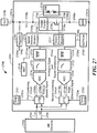
- FIG. 2 another example of a prior art magnetic field sensor 200 is responsive to a gear 214 having gear teeth, e.g., gear teeth 214a, 214b, 214c.
- the magnetic field sensor 200 includes three magnetic field sensing elements 202, 204, 206 coupled to an electronic circuit 210.
- the magnetic field sensing elements 202, 204 are separated in a direction perpendicular to an axis 216 by a distance between about 1.5 millimeters and about 3.0 millimeters, and the magnetic field sensing element 206 is located midway between the magnetic field sensing elements 202, 204.
- the three magnetic field sensing elements 202, 204, 206 and an electronic circuit 210 can be disposed upon (i.e., integrated within or upon) a substrate 208.
- the magnetic field sensing elements 202, 204, 206 are shown to be Hall elements with an exaggerated size, and rotated out of the plane of the substrate 208.
- the Hall elements 202, 204, 206 are shown to be on top of the substrate 208, but it will be appreciated that Hall elements are usually disposed upon or within a surface of a substrate of an integrated circuit.
- the magnetic field sensor 200 can also include a magnet 212.
- the magnet 212 is configured to generate a magnetic field, which is generally directed along an axis 216 at the position of the magnetic field sensing elements 202, 204, 206.
- the electronic circuit 210 is configured to generate an output signal (not shown).
- An exemplary electronic circuit 210 is described below in conjunction with FIG. 2A . Let it suffice here to say that the electronic circuit generates differences of signals. Thus, it will be apparent that the magnetic field sensor 200 is an edge detector and not a tooth detector.
- the output signal when the gear 214 is rotating, is indicative speed of rotation of the gear 214 and also indicative of positions of edges of the gear teeth.
- the magnetic field sensor 200 is unable to provide a TPOS function, and, when the gear 214 is stationary, is unable to identify whether the magnetic field sensing elements 202, 204, 206 are proximate to a gear tooth or a valley in the gear 214.
- the magnet 212 can be comprised of one uniform material, and can have no central core, which is shown and described in conjunction with FIG. 1 . However, in other embodiments, the magnet 212 can have a central core the same as or similar to that shown and described in conjunction with FIG. 1 .
- the magnetic field sensor 200 uses the three magnetic field sensing elements 202, 204, 206 to generate a respective three differential signals 202a, 202b, and 204a, 204b, and 206a, 206b.
- the simple magnet 212 does not provide the low baseline of a magnet with a core, differences of the above differential signals result in the effect of a low baseline.
- a differencing of the above differential signals results in a zero electronic signal.
- an example of a prior art electronic circuit 250 can be the same as or similar to electronic circuit 210 of FIG. 2 .
- the electronic circuit 250 can include amplifiers 258, 260, 262 coupled to receive differential signals 252a, 252b, and 254a, 254b, and 256a, 256b, respectively.
- the differential signal 252a, 252b can be the same as or similar to the differential signal 202a, 202b, the differential signal 254a, 254b can be the same as or similar to the differential signals 204a, 204b, and the differential signal 256a, 256b can be the same as or similar to the differential signal 206a, 206b generated, respectively, by the magnetic field sensing elements 202, 204, 206 of FIG. 2 .
- the amplifiers 258, 260, 262 are configured to generate amplified signals 258a, 260a, 262a, respectively.
- the amplified signals 258a, 260a are received by a first differencing module 264, which is configured to generate a first difference signal 264a.
- the amplified signals 260a, 262a are received by a second differencing module 266, which is configured to generate a second difference signal 266a.
- the electronic circuit 250 includes two precision rotation detector channels, described above in conjunction with FIG. 1A .
- a AGCs 270, 276 can be the same as or similar to the AGC 56 of FIG. 1A .
- Precisions rotation detectors 272, 278 can be the same as or similar to the precision rotation detector 60 of FIG. 1A .
- the precision rotation detector 272 can generate a precision rotation detector output signal 272a and the precision rotation detector 278 can generate a precision rotation detector output signal 278a.
- the precision rotation detector output signals 272a, 278a can be the same as or similar to the precision rotation detector output signal 60a of FIG. 1A .
- a speed and direction module 274 can be coupled to receive the precision rotation detector output signals 272a, 278a.
- the precision rotation detector output signals 272a, 278a are at relative phases that are determined by a direction of rotation of the gear 214. It should also be apparent that the state transition rates of the precision rotation detector output signals 272a, 278a are representative of a speed of rotation of the gear 214.
- the speed and direction module is configured to generate an output signal that can be representative of at least one of the speed of rotation or a direction of rotation of the gear 214.
- the output signal 62a is representative of both the speed of rotation and the direction of rotation.
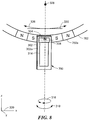
- a magnetic field sensor 300 is responsive to a gear 322 having gear teeth, e.g., gear teeth 322a, 322b, 322c.
- the gear 322 can be a ferromagnetic gear, i.e., a ferromagnetic target object having ferromagnetic teeth, also ferromagnetic objects, and referred to herein as target features.
- the magnetic field sensor 300 can include a substrate 302 with a major surface 302a.
- the magnetic field sensor 300 can include magnetic field sensing elements 304 disposed on the major surface 302a of the substrate 302. Further details of the magnetic field sensing elements 304 are described below. However, let is suffice here to say that the magnetic field sensing elements 304 can include at least two magnetoresistance elements.
- the magnetic field sensing elements 304 can be coupled to or within an electronic circuit 314 also disposed on the major surface 302a of the substrate 302.
- the magnetic field sensor 300 can also include a magnet 332.
- the magnet 332 is configured to generate a magnetic field, which is generally directed along an axis 308 at the position of the magnetic field sensing elements 304, and is generally parallel to the major surface 302a of the substrate 302.
- the magnetic field sensing elements 304 have respective maximum response axes parallel to the major surface 302a of the substrate 302. In some embodiments, the maximum response axes are parallel to each other. In some embodiments, the maximum response axes are substantially parallel to the axis 308. In other embodiments, the maximum response axes are substantially perpendicular to the axis 308.
- the magnetic field sensing elements 304 are disposed at positions such that an axis (e.g., 308) between (i.e., passing through) the magnetic field sensing elements 304 does not intersect the gear 322.
- the axis (e.g., 308) between (i.e., passing through) the magnetic field sensing elements 304 is substantially parallel to a tangent 330 to a direction of movement, e.g., 326, of the gear 322.
- a line between north (N) and south (S) poles of the magnet 332 is substantially parallel to the major surface 302a of the substrate 302, and is substantially parallel to the axis (e.g., 308) between (i.e., passing through) the two magnetic field sensing elements 304, 306.
- the line between the north and south poles of the magnet 332 does not intersect the gear 322 and is not in a direction toward the gear 322.
- the electronic circuit 314 is configured to generate an output signal (not shown).
- An exemplary electronic circuit 314 is described below in conjunction with FIG. 26 . Let it suffice here to say that the electronic circuit 314 generates a difference of signals and a sum of signals. Thus, it will become apparent that the magnetic field sensor 300 is both an edge detector and a tooth detector.
- the output signal when the gear 322 is rotating, is indicative of a speed of rotation of the gear 322 and also indicative of positions of edges of the gear teeth.
- the magnetic field sensor 300 is able to provide a tooth detecting (e.g., TPOS) function, and, when the gear 322 is stationary, is able to identify whether the magnetic field sensing elements 304 are proximate to a gear tooth or a valley in the gear 322.
- the magnet 332 can be comprised of one uniform material, and can have no central core, which is shown and described in conjunction with FIG. 1 . However, in other embodiments, the magnet 332 can have a central core the same as or similar to that shown and described in conjunction with FIG. 1 . Such core can have an axis aligned with an axis 324.
- the magnetic field sensor 300 can be rotated in a direction 316 to a next position three hundred and sixty degrees apart from the position shown, with no degradation of performance. However, intermediate rotations may result in a degradation of performance.
- the magnetic field sensor 300 can be rotated in a direction of and arrow 318 with a center of rotation anywhere along a line 324, through approximately +/- twenty degrees, without substantial degradation of performance.
- the magnetic field sensing elements 304 are magnetoresistance elements.
- the magnetic field sensor 300 is shown in an arrangement wherein the substrate 302, and the magnetic field sensing elements 304 thereon, overlap the gear 322.
- the magnetic field sensor 300 is shown in an arrangement rotated about the x-axis ninety degrees outward from the page or ninety degrees into the page as compared to the arrangement shown in FIG. 3 .
- the magnetic field sensing elements 304 remain disposed proximate to the gear 322.
- a magnetic field sensor 600 is like the magnetic field sensor 300 of FIG. 3 , but the magnetic field sensor 600 has a different magnet 602.
- the magnetic field sensor 600 has the different magnet 602 for which a line between north (N) and south (S) poles of the magnet 602 is substantially parallel to the major surface 302a of the substrate 302, but substantially perpendicular to the axis (e.g., 308) between (i.e., passing through) the magnetic field sensing elements.
- the line between the north and south poles of the magnet 602 is in a direction toward the gear 322.
- the magnet 602 is a simple magnet without a core, such core described above in conjunction with FIG. 1 . In other embodiments, the magnet 602 has a core with an axis along the line 324.
- FIGS. 7-9 described below show the same or similar magnetic field sensors for sensing movement of a ring magnet. Comments made above about edge detectors, tooth detectors, and TPOS functions apply in a similar way when sensing a ring magnet.
- a magnetic field sensor 700 is like the magnetic field sensor 300 of FIG. 3 .
- the magnetic field sensor 700 has no internal magnet. Instead, the magnetic field sensor 700 is responsive to passing magnetic domains, e.g., 702a, of a ring magnet 702.
- the magnetic domains of the ring magnet 702 are polarized parallel to the page. In some other embodiments, the magnetic domains of the ring magnet 702 are polarized perpendicular to the page.
- the magnetic field sensor 700 is shown in an arrangement wherein the substrate 302, and the magnetic field sensing elements 304 thereon, overlap the ring magnet 702. It should be apparent that the magnetic fields sensor 700 could be rotated one hundred eighty degrees about the y-axis such that the magnetic field sensing elements 304 still overlap the magnetic domains, e.g., 702a, of the ring magnet 702. A line perpendicular to the surface 302a of the substrate 302 and passing through the magnetic field sensing elements 304 intersects the ring magnet 702.
- the magnetic field sensor 700 is shown in an arrangement rotated about the x-axis ninety degrees outward from the page or ninety degrees into the page as compared to the arrangement shown in FIG. 5 .
- the magnetic field sensing elements 304 remained disposed proximate to the ring magnet 702.
- designations V1, V2 are shown to designate two signals. It should be understood that these designations indicate a logical relationship between similar designations in similar figures. However, these designations do not indicate that a signal so designated in one figure is the same signal as one with the same designation in other figures.
- R1, R2 are shown to designate two fixed resistors. It should be understood that these designations indicate a logical relationship between similar designations in similar figures. However, these designations do not indicate that a resistor so designated in one figure is the same resistor as one with the same designation in other figures.
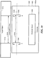
- a magnetic field sensor 1000 can include a substrate 1002 having a surface 1002a, which is one of two parallel major surfaces of the substrate 1002.
- Two magnetoresistance elements 1004, 1006 can be disposed upon the surface 1002a along an axis 1010.
- the two magnetoresistance elements 1004, 1006 (A, B) can be part of or coupled to an electronic circuit 1008, which is also disposed upon or within the surface 1002a of the substrate 1002.
- the two magnetoresistance elements 1004, 1006 (A, B) can be the same as or similar to the magnetic field sensing elements 304 of FIGS. 3-9 .
- the axis 1010 can be parallel to the axis 308 of FIGS. 3-9 .
- Magnetoresistance elements e.g., 1004, 1006 (A, B) are shown in all embodiments herein to be in the form of so-called "yokes," which have a C-shape (or a reverse C-shape).
- the yokes can have longest yoke axes substantially perpendicular to the axis 1010.
- Advantages of yoke shapes are known. It will be understood that other magnetoresistance elements used in embodiments herein can have other shapes, for example, lines, polylines, or rectangles.
- Maximum response axes of the magnetoresistance elements 1004, 1006 (A, B) can be parallel to and along the axis 1010 and in the same direction. It should be understood that the magnetoresistance elements 1004, 1006 (A, B) having maximum response axes parallel to the axis 1010 are also responsive to magnetic fields at other angles in the plane of the substrate 1002 (and also out of the plane of the substrate 1002). The degree to which the magnetoresistance elements 1004, 1006 (A, B) are responsive to magnetic fields at other angles not parallel to the axis 1010 (and not perpendicular to the longest yoke axes) is determined by a magnitude of a geometric projection of the magnetic field at the other angle onto the axis 1010. Thus, the term "projected magnetic field" is used below to describe this projection.
- the degree to which the magnetoresistance elements 1004, 1006 (A, B) are responsive to magnetic fields at other angles not parallel to the axis 1010 is determined by a magnitude of a geometric projection of the magnetic field at the other angle onto an axis that is perpendicular to the longest axes of the yoke shapes. This is also referred to herein as a projected magnetic field.
- the magnetic field sensor 1000 is responsive to movement of a ferromagnetic target object 1012 having features, e.g., 1012a, with width 1014.
- the ferromagnetic target object 1012 can be the same as or similar to the gear 322 of FIGS. 3-6 or the ring magnet 702 of FIGS. 7-9 .
- the features, e.g., 1012a can be the same as or similar to the gear teeth, e.g., 322a, of FIGS. 3-6 or the magnetic regions, e.g., 702a, of the ring magnet 702 of FIGS. 7-9 .
- the magnetic field sensor 1000 can be the same as or similar to the magnetic field sensor 300 of FIGS. 3-5 , the magnetic field sensor 600 of FIG. 6 , and the magnetic field sensor 700 of FIGS. 7-9 . However, the magnetic field sensor 1000 is not shown in the rotated position described above in conjunction with FIGS. 5 and 9 . Nevertheless the magnetic field sensor 1000 can be rotated into or out of the page in the same way.
- the two magnetoresistance elements 1004, 1006 (A, B) have a separation 1016 between about one half and about one and one half of the width 1014 of the target feature 1012a, for example, a gear tooth of a ferromagnetic gear or a magnetic domain of a ferromagnetic ring magnet.
- the two magnetoresistance elements 1004, 1006 (A, B) have a separation 1016 between about one half and about twice the width 1014 of the target feature 1012a.
- the separation 1016 is much smaller than half of the width 1014, for example, one one hundredth of the width 1014, or larger than twice the width 1014.
- the separation 1016 is about equal to the width 1014 of the target feature 1012a, for example, a gear tooth of a ferromagnetic gear or a magnetic domain of a ferromagnetic ring magnet.
- the two magnetoresistance elements 1004, 1006 can generate two output signals.
- Figures shown and described below are representative of a variety of ways in which the two magnetic field sensing elements 1004, 1006 can generate two output signals.
- any magnetoresistance element(s) e.g., 1004 (A)
- any magnetoresistance element(s) e.g., 1006 (B)
- any magnetoresistance element(s) e.g., 1004 (A)
- any magnetoresistance element(s) e.g., 1006 (B)
- any magnetoresistance element(s) e.g., 1006 (B)
- the magnetic field sensor 1000 can include a magnet.
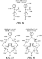
- the two magnetoresistance elements 1004, 1006 are coupled between a respective current sources 1102, 1104 and ground.
- a difference V1-V2 of the two output signals V1, V2 has a maximum (positive or negative) instantaneous value.
- the target feature 1012a can be a tooth, e.g., 322a, (or alternatively, a valley) of the gear 322 of FIG. 3 , or a magnetic domain, e.g. 702a, (north, or alternatively, south) of the ring magnet 702 of FIG. 7 .
- the difference V1-V2 is representative of a proximity of a tooth or proximity of a magnetic domain, and is, therefore, representative of a "feature" of the ferromagnetic target object.
- a sum V1+V2 of the two output signals V1, V2 has a maximum (positive or negative) instantaneous value.
- the sum V1+V2 is representative of a proximity of an edge, and is, therefore, representative of an "edge" of the ferromagnetic target object.
- a magnetic field sensor using both the difference V1-V2 of the two signals V1, V2 and also the sum V1+V2 of the two signals V1, V2 can operate both as a tooth detector and a an edge detector, respectively.
- the tooth detector capability allows a magnetic field sensor using the two magnetoresistance elements 1004, 1006, coupled as shown, to operate with a true-power-on-state (TPOS) function.
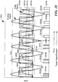
- the two signals V1, V2 here and in figures below can be used to determine both speed and direction of a moving ferromagnetic object. It will also become apparent from discussion below that the sum V1+V2 of the two signals is ninety degrees apart from the difference V1-V2 of the two signals.
- the two magnetoresistance elements 1004, 1006 are coupled in a bridge arrangement 1200 with fixed resistors 1202, 1204, also referred to herein as resistors R1, R2.
- the fixed resistors 1202, 1204 can be magnetically insensitive elements (or less sensitive elements) having some layers like a magnetoresistance element, as described, for example, in U.S. Patent Number 7,777,607, issued August 17, 2010 .
- Such magnetically insensitive elements tend to have a temperature coefficient the same as that of the two magnetoresistance elements 1104, 1106 (A, B), and thus, the bridge 1200 can be substantially insensitive to temperature variations.
- the bridge 1200 can be powered by a voltage source 1206.
- Designations V1 and V2 are used below for clarity as discussed above.
- the two output signals V1, V2 are treated as one differential signal V1, V2.
- the two output signals V1, V2 are treated separately.
- a difference V1-V2 of the two output signals V1, V2 has a maximum (positive or negative) instantaneous value.
- the target feature 1012a can be a tooth, e.g., 322a, (or alternatively, a valley) of the gear 322 of FIG. 3 , or a magnetic domain, e.g. 702a, (north, or alternatively, south) of the ring magnet 702 of FIG. 7 .
- the difference V1-V2 is representative of a proximity of a tooth or proximity of a magnetic domain, and is, therefore, representative of a "feature" of the ferromagnetic target object.
- a sum V1+V2 of the two output signals V1, V2 has a maximum (positive or negative) instantaneous value.
- the sum V1+V2 is representative of a proximity of an edge, and is, therefore, representative of an "edge" of the ferromagnetic target object.
- a magnetic field sensor using both the difference V1-V2 of the two signals V1, V2 and also the sum V1+V2 of the two signals V1, V2 can operate both as a tooth detector and a an edge detector, respectively.
- the tooth detector capability allows a magnetic field sensor using the two magnetoresistance elements 1004, 1006 (A, B), coupled as shown, to operate with a true-power-on-state (TPOS) function.
- the two magnetoresistance elements 1004, 1006 are coupled in a bridge arrangement 1300 with fixed resistors 1302, 1304 (also referred to herein as R1, R2).
- the fixed resistors 1302, 1304 can be magnetically insensitive elements having some layers like a magnetoresistance element, as described, for example, in U.S. Patent Number 7,777,607, issued August 17, 2010 .
- the bridge 1300 can be powered by a voltage source 1306.
- Designations V1 and V2 are used below for clarity.
- the two output signals V1, V2 are treated as one differential signal V1, V2.
- the two output signals V1, V2 are treated separately.
- a sum V1+V2 of the two output signals V1, V2 has a maximum (positive or negative) instantaneous value.
- the target feature 1012a can be a tooth, e.g., 322a, (or alternatively, a valley) of the gear 322 of FIG. 3 , or a magnetic domain, e.g. 702a, (north, or alternatively, south) of the ring magnet 702 of FIG. 7 .
- the sum V1+V2 is representative of a proximity of a tooth or proximity of a magnetic domain, and is, therefore, representative of a "feature" of the ferromagnetic target object.
- a difference V1-V2 of the two output signals V1, V2 has a maximum (positive or negative) instantaneous value.
- the difference V1-V2 is representative of a proximity of an edge, and is, therefore, representative of an "edge" of the ferromagnetic target object.
- a magnetic field sensor using both the sum V1+V2 of the two signals V1, V2 and also the difference V1-V2 of the two signals V1, V2 can operate both as a tooth detector and a an edge detector, respectively.
- the tooth detector capability allows a magnetic field sensor using the two magnetoresistance elements 1004, 1006 (A, B), coupled as shown, to operate with a true-power-on-state (TPOS) function.
- FIGS. 12 and 13 above show particular bridge arrangements, there are other possible bridge arrangements that should be apparent.
- the magnetic field sensing elements 1004, 1006 can be interchanged in position.
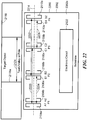
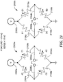
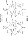
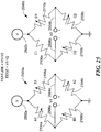
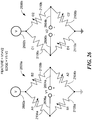
- a magnetic field sensor 1400 can include a substrate 1402 having a surface 1402a, which is one of two parallel major surfaces of the substrate 1402.
- magnetoresistance elements 1404, 1406, 1408, 1410 can be disposed upon the surface 1402a.
- the four magnetoresistance elements 1404, 1406, 1408, 1410 (A, B, C, D) can be part of or coupled to an electronic circuit 1412, which is also disposed upon or within the surface 1402a of the substrate 1412.
- the four magnetoresistance elements 1404, 1406, 1408, 1410 (A, B, C, D) can be the same as or similar to the magnetic field sensing elements 304 of FIGS. 3-9 .
- Maximum response axes of the magnetoresistance elements 1404, 1410 can be parallel to and along an axis 1414.
- Maximum response axes of the magnetoresistance elements 1406, 1408 (B, C) can be parallel to and along an axis 1416.
- the axes 1414, 1416 can be parallel to the axis 308 of FIGS. 3-9 .
- Angles of magnetic fields are discussed above in conjunction with FIG. 10 .
- the term "projected magnetic field” is used to describe geometric projections of magnetic fields upon the axes 1414, 1416.
- the magnetic field sensor 1400 is responsive to movement of a ferromagnetic target object 1418 having features, e.g., 1418a, with width 1424.
- the ferromagnetic target object 1418 can be the same as or similar to the gear 322 of FIGS. 3-6 or the ring magnet 702 of FIGS. 7-9 .
- the features, e.g., 1418a can be the same as or similar to the gear teeth, e.g., 322a, of FIGS. 3-6 or the magnetic regions, e.g., 502a, of the ring magnet 702 of FIGS. 7-9 .
- the magnetic field sensor 1400 can be the same as or similar to the magnetic field sensor 300 of FIGS. 3-5 , the magnetic field sensor 600 of FIG. 6 , and the magnetic field sensor 700 of FIGS. 7-9 . However, the magnetic field sensor 1400 is not shown in the rotated position described above in conjunction with FIGS. 5 and 9 . Nevertheless the magnetic field sensor 1400 can be rotated into or out of the page in the same way.
- the magnetoresistance elements 1404, 1410 are disposed along the axis 1414 proximate to the ferromagnetic target object 1418 and the magnetoresistance elements 1406, 1408 are disposed along the axis 1416 more distant from the ferromagnetic target object 1418.
- the axes 1414, 1416 can be parallel to the axis 308 of FIGS. 3-9 .
- the two magnetoresistance elements 1404, 1408 (A, C) have a separation 1420 between about one half and about one and one half of the width 1424 of the target feature 1418a, for example, a gear tooth of a ferromagnetic gear or a magnetic domain of a ferromagnetic ring magnet.
- the two magnetoresistance elements 1404, 1408 (A, C) have a separation 1420 between about between about one half and about twice the width 1424 of the target feature 1418a.
- the separation 1420 is much smaller than half of the width 1424, for example, one one hundredth of the width 1424, or larger than twice the width 1424.
- the separation 1420 is about equal to the width 1424 of the target feature 1418a.
- the two magnetoresistance elements 1406, 1410 (B, D) have a separation 1422 between about one half and about one and one half of the width 1424 of the target feature 1418a, for example, a gear tooth of a ferromagnetic gear or a magnetic domain of a ferromagnetic ring magnet.
- the two magnetoresistance elements 1406, 1410 (B, D) have a separation 1422 between about one half and about twice the width 1424 of the target feature 1418a.
- the separation 1422 is much smaller than half of the width 1424, for example, one one hundredth of the width 1424, or larger than twice the width 1424.
- the separation 1422 is about equal to the width 1424 of the target feature 1418a.
- the two magnetoresistance elements 1404, 1406 (A, B) have a separation 1428 between about one half and about one and one half of the width 1424 of the target feature 1418a. In some other embodiments, the two magnetoresistance elements 1404, 1406 (A, B) have a separation 1428 between about one half and about twice the width 1424 of the target feature 1418a. In some embodiments used in examples below, the separation 1428 is about equal to the width 1424 of the target feature 1418a. However, in other embodiments, the separation 1428 is much smaller than half of the width 1424, for example, one one hundredth of the width 1424, or larger than twice the width 1424.
- the separation 1428 is about equal to the width 1424 of the target feature 1418a.
- the two magnetoresistance elements 1408, 1410 have a separation 1430 between about one half and about one and one half of the width 1424 of the target feature 1418a.
- the two magnetoresistance elements 1408, 1410 (C, D) have a separation 1430 between about one half and about twice the width 1424 of the target feature 1418a.
- the separation 1430 is about equal to the width 1424 of the target feature 1418a.
- the separation 1430 is much smaller than half of the width 1424, for example, one one hundredth of the width 1424 or larger than twice the width 1424.
- the separation 1430 is about equal to the width 1424 of the target feature 1418a.
- the four magnetoresistance elements 1404, 1406, 1408, 1410 can generate at least two output signals.
- Figures shown and described below are representative of a variety of ways in which the four magnetoresistance elements 1404, 1406, 1408, 1410 (A, B, C, D) can generate at least two output signals.
- the target feature 1418a with a width 1424 equal to the spacings 1420, 1422 when the target feature 1418a is centered about (i.e., between) the four magnetoresistance elements 1404, 1406, 1408, 1410 (A, B, C, D), it can be shown that any magnetoresistance element(s) (e.g., 1404, 1406 (A, B)) on one side of a center of the target feature 1418a experiences a projected magnetic field pointed in one direction along the axes 1414, 1416, and any magnetoresistance element(s) (e.g., 1408, 1410 (C, D)) on the other side of the center of the target feature 1418a experiences a projected magnetic field pointed in the other direction.
- any magnetoresistance element(s) e.g., 1404, 1406 (A, B)
- any magnetoresistance element(s) e.g., 1408, 1410 (C, D)
- any magnetoresistance element(s) e.g., 1404, 1406 (A, B)
- any magnetoresistance element(s) e.g., 1408, 1410 (C, D)
- any magnetoresistance element(s) e.g., 1408, 1410 (C, D)
- the two magnetoresistance elements 1406, 1408 (B, C) experience projected magnetic fields pointed in the same direction along the axis 1416, but opposite in direction to the projected magnetic fields experienced by the two magnetoresistance elements 1404, 1410 (A, D).
- resistance of both of the two magnetoresistance elements 1406, 1408 (B, C) change in the same direction but opposite to the resistance change of the two magnetoresistance elements 1404, 1410 (A, D).
- the resistance change of the two magnetoresistance elements 1406, 1408 (B, C) is small, if any.
- the magnetic field sensor 1400 can include a magnet.
- a magnetic field sensor 1500 can include a substrate 1502 having a surface 1502a, which is one of two parallel major surfaces of the substrate 1502.
- the four magnetoresistance elements 1404, 1406, 1408, 1410 can be disposed upon the surface 1502a along an axis 1514.
- the four magnetoresistance elements 1404, 1406, 1408, 1410 (A, B, C, D) can be part of or coupled to the electronic circuit 1412, which is also disposed upon or within the surface 1502a of the substrate 1502.
- the four magnetoresistance elements 1404, 1406, 1408, 1410 (A, B, C, D) can be the same as or similar to the magnetic field sensing elements 304 of FIGS. 3-9 .
- the axis 1514 can be parallel to the axis 308 of FIGS. 3-9 .
- Maximum response axes of the four magnetoresistance elements 1404, 1406, 1408, 1410 can be parallel to and along an axis 1514, and in the same direction. Angles of magnetic fields are discussed above in conjunction with FIG. 10 . As described above, the term "projected magnetic field" is used to describe geometric projections of magnetic fields upon the axis 1514.
- the magnetic field sensor 1500 is responsive to movement of the ferromagnetic target object 1418.
- the four magnetoresistance elements 1404, 1406, 1408, 1410 are disposed along the axis 1514 proximate to the ferromagnetic target object 1418.
- the magnetic field sensor 1500 can be the same as or similar to the magnetic field sensor 300 of FIGS. 3-5 , the magnetic field sensor 600 of FIG. 6 , of the magnetic field sensor 700 of FIGS. 7-9 . However, the magnetic field sensor 1500 is not shown in the rotated position described above in conjunction with FIGS. 5 and 9 . Nevertheless the magnetic field sensor 1500 can be rotated into or out of the page in the same way.
- the four magnetoresistance elements 1404, 1406, 1408, 1410 can be the same as or similar to the magnetic field sensing elements 304 of FIGS. 3-9 .
- the ferromagnetic target object 1418 can be the same as or similar to the gear 322 of FIGS. 3-6 or the ring magnet 702 of FIGS. 7-9 .
- the axis 1514 can be parallel to the axis 308 of FIGS. 3-9 .
- the two magnetoresistance elements 1404, 1408 (A, C) have a separation 1520 between about one half and about one and one half of the width 1424 of the target feature 1418a, for example, a gear tooth of a ferromagnetic gear or a magnetic domain of a ferromagnetic ring magnet.
- the two magnetoresistance elements 1404, 1408 (A, C) have a separation 1520 between about one half and about twice the width 1424 of the target feature 1418a.
- the separation 1520 is much smaller than half of the width 1424, for example, one one hundredth of the width 1424 or larger than twice the width 1424.
- the separation 1520 is about equal to the width 1424 of the target feature 1418a.
- the two magnetoresistance elements 1406, 1410 (B, D) have a separation 1522 between about one half and about one and one half of the width 1424 of the target feature 1418a, for example, a gear tooth of a ferromagnetic gear or a magnetic domain of a ferromagnetic ring magnet.
- the two magnetoresistance elements 1406, 1410 (B, D) have a separation 1522 between about one half and about twice the width 1424 of the target feature 1418a.
- the separation 1522 is much smaller than half of the width 1424, for example, one one hundredth of the width 1424 or larger than twice the width 1424.
- the separation 1522 is about equal to the width 1424 of the target feature 1418a.
- the two magnetoresistance elements 1404, 1406 (A, B) have a separation 1524 between about one half and about one and one half of the width 1424 of the target feature 1418a. In some other embodiments, the two magnetoresistance elements 1404, 1406 (A, B) have a separation 1524 between about one half and about twice the width 1424 of the target feature 1418a. However, in other embodiments, the separation 1424 is much smaller than half of the width 1424, for example, one one hundredth of the width 1424 or larger than twice the width 1424.
- the separation 1524 is about equal to the width 1424 of the target feature 1418a.
- the two magnetoresistance elements 1408, 1410 have a separation 1526 between about one half and about one and one half of the width 1424 of the target feature 1418a.
- the two magnetoresistance elements 1408, 1410 (C, D) have a separation 1526 between about one half and twice the width 1424 of the target feature 1418a.
- the separation 1526 is much smaller than half of the width 1424, for example, one one hundredth of the width 1424 or larger than twice the width 1424.
- the separation 1526 is about equal to the width 1424 of the target feature 1418a.
- the four magnetoresistance elements 1404, 1406, 1408, 1410 can generate at least two output signals.
- Figures shown and described below are representative of a variety of ways in which the four magnetoresistance elements 1404, 1406, 1408, 1410 (A, B, C, D) can generate at least two output signals.
- the target feature 1012a with a width 1014 equal to the spacings 1520, 1522 when the target feature 1418a is centered about (i.e., between) the four magnetoresistance elements 1404, 1406, 1408, 1410 (A, B, C, D), it can be shown that any magnetoresistance element(s) (e.g., 1404, 1406 (A, B)) on one side of a center of the target feature 1418a experiences a projected magnetic field pointed in one direction along the axis 1514, and any magnetoresistance element(s) (e.g., 1408, 1410 (C, D)) on the other side of the center of the target feature 1418a experiences a projected magnetic field pointed in the other direction.
- any magnetoresistance element(s) e.g., 1404, 1406 (A, B)
- any magnetoresistance element(s) e.g., 1408, 1410 (C, D)
- any magnetoresistance element(s) e.g., 1404, 1406 (A, B)
- any magnetoresistance element(s) e.g., 1408, 1410 (C, D)
- any magnetoresistance element(s) e.g., 1408, 1410 (C, D)
- the two magnetoresistance elements 1406, 1408 (B, C) experience projected magnetic fields pointed in the same direction along the axis 1514, but opposite in direction from the projected magnetic fields experienced by the two magnetoresistance elements 1404, 1410 (A, D).
- resistance of both of the two magnetoresistance elements 1406, 1408 (B, C) change in the same direction but opposite to the resistance change of the two magnetoresistance elements 1404, 1410 (A, D).
- the magnetic field sensor 1400 can include a magnet.
- the four magnetoresistance elements 1404, 1406, 1408, 1410 are coupled to respective current sources 1602, 1604, 1606, 1608 resulting in respective signals 1610, 1612, 1614, 1616, also referred to generically herein as signals VA, VB, VC, VD, respectively.
- a difference V1-V2 of the two output signals V1, V2 has a maximum (positive or negative) instantaneous value when an edge of the target feature 1418a is centered about (i.e., between) the four magnetoresistance elements 1404, 1406, 1408, 1410 (A, B, C, D). Largest signals can be achieved when the distances 1520, 1522 are equal to the distance 1424.
- a magnetic field sensor using the four magnetoresistance elements 1404, 1406, 1408, 1410 (A, B, C, D) and using both the sum V1+V2 of the two signals V1, V2 and also the difference V1-V2 of the two signals V1, V2 can operate both as a tooth detector and a an edge detector, respectively.
- the tooth detector capability allows a magnetic field sensor using the four magnetoresistance elements 1404, 1406, 1408, 1410 (A, B, C, D) to operate with a true-power-on-state (TPOS) function.
- TPOS true-power-on-state
- FIG. 17 in which like elements of FIGS. 14 and 15 are shown having like reference designations, the four magnetoresistance elements 1404, 1406, 1408, 1410 (A, B, C, D) are coupled in a bridge arrangement 1700.
- the bridge 1700 can be powered by a voltage source 1702.
- Designations V1 and V2 are used below for clarity.
- the two output signals V1, V2 are treated as one differential signal V1, V2.
- the two output signals V1, V2 are treated separately.
- a difference V1-V2 of the two signals V1, V2 has a maximum (positive or negative) instantaneous value when the object feature 1418a of FIGS. 14 and 15 , but particularly FIG. 14 , is centered about the four magnetoresistance elements 1404, 1406, 1408, 1410 (A, B, C, D).
- the difference V1-V2 therefore, provides a feature signal.
- a sum V1+V2 of the two output signals V1, V2 has a maximum (positive or negative) instantaneous value when an edge of the target feature 1418a is centered about (i.e., between) the four magnetoresistance elements 1404, 1406, 1408, 1410 (A, B, C, D).
- a magnetic field sensor using the bridge 1700 and using both the difference V1-V2 of the two signals V1, V2 and also the sum V1+V2 of the two signals V1, V2 can operate both as a tooth detector and a an edge detector, respectively.
- the tooth detector capability allows a magnetic field sensor using the four magnetoresistance elements 1404, 1406, 1408, 1410 (A, B, C, D) to operate with a true-power-on-state (TPOS) function.
- the bridge 1700 is best suited for the arrangement of FIG. 14 , but can also function with the arrangement of FIG. 15 .
- FIG. 18 in which like elements of FIGS. 14 and 15 are shown having like reference designations, the four magnetoresistance elements 1404, 1406, 1408, 1410 (A, B, C, D) are coupled in a bridge arrangement 1800.
- the bridge 1800 can be powered by a voltage source 1802.
- Designations V1 and V2 are used below for clarity.
- the two output signals V1, V2 are treated as one differential signal V1, V2.
- the two output signals V1, V2 are treated separately.
- a difference V1-V2 of the two signals V1, V2 has a maximum (positive or negative) instantaneous value when the object feature 1418a of FIGS. 14 and 15 is centered about the four magnetoresistance elements 1404, 1406, 1408, 1410 (A, B, C, D).
- the difference V1-V2 therefore, provides a feature signal.
- a sum V1+V2 of the two output signals V1, V2 has a maximum (positive or negative) instantaneous value when an edge of the target feature 1418a is centered about (i.e., between) the four magnetoresistance elements 1404, 1406, 1408, 1410 (A, B, C, D).
- a magnetic field sensor using the bridge 1700 and using both the difference V1-V2 of the two signals V1, V2 and also the sum V1+V2 of the two signals V1, V2 can operate both as a tooth detector and a an edge detector, respectively.
- the tooth detector capability allows a magnetic field sensor using the four magnetoresistance elements 1404, 1406, 1408, 1410 (A, B, C, D) to operate with a true-power-on-state (TPOS) function.
- the bridge 1800 is well suited for the arrangements of FIGS. 14 and 15 .
- FIG. 19 in which like elements of FIGS. 14 and 15 are shown having like reference designations, the four magnetoresistance elements 1404, 1406, 1408, 1410 (A, B, C, D) are coupled in a bridge arrangement 1900.
- the bridge 1900 can be powered by a voltage source 1902.
- Designations V1 and V2 are used below for clarity.
- the two output signals V1, V2 are treated as one differential signal V1, V2.
- the two output signals V1, V2 are treated separately.
- a difference V1-V2 of the two output signals V1, V2 has a maximum (positive or negative) instantaneous value when an edge of the target feature 1418a is centered about (i.e., between) the four magnetoresistance elements 1404, 1406, 1408, 1410 (A, B, C, D).
- a magnetic field sensor using the bridge 1900 and using both the sum V1+V2 of the two signals V1, V2 and also the difference V1-V2 of the two signals V1, V2 can operate both as a tooth detector and a an edge detector, respectively.
- the tooth detector capability allows a magnetic field sensor using bridge 1900 to operate with a true-power-on-state (TPOS) function.
- the bridge 1900 is best suited for the arrangement of FIG. 14 , but can also function with the arrangement of FIG. 15 .
- FIG. 20 in which like elements of FIGS. 14 and 15 are shown having like reference designations, the four magnetoresistance elements 1404, 1406, 1408, 1410 (A, B, C, D) are coupled in a bridge arrangement 2000.
- the bridge 2000 can be powered by a voltage source 2002.
- Designations V1 and V2 are used below for clarity.
- the two output signals V1, V2 are treated as one differential signal V1, V2.
- the two output signals V1, V2 are treated separately.
- a difference V1-V2 of the two output signals V1, V2 has a maximum (positive or negative) instantaneous value when an edge of the target feature 1418a is centered about (i.e., between) the four magnetoresistance elements 1404, 1406, 1408, 1410 (A, B, C, D).
- a magnetic field sensor using the bridge 2000 and using both the sum V1+V2 of the two signals V1, V2 and also the difference V1-V2 of the two signals V1, V2 can operate both as a tooth detector and a an edge detector, respectively.
- the tooth detector capability allows a magnetic field sensor using bridge 2000 to operate with a true-power-on-state (TPOS) function.
- the bridge 2000 is well suited for the arrangements of FIGS. 14 and 15 .
- FIGS. 17-20 While various bridge arrangements are shown in FIGS. 17-20 , there are other similar bridge arrangements that can be used to generate a feature signal and an edge signal.
- a magnetic field sensor 2100 can include a substrate 2102 having a surface 2102a, which is one of two parallel major surfaces of the substrate 2102.
- Eight magnetoresistance elements 2104a, 2104b, 2106a, 2106b, 2108a, 2108b, 2110a, 2110b can be disposed upon the surface 2102a.
- the eight magnetoresistance elements 2104a, 2104b, 2106a, 2106b, 2108a, 2108b, 2110a, 2110b (Al, A2, B1, B2, C1, C2, D1, D2) can be arranged in proximate pairs P1, P2, P3, P4.
- the eight magnetoresistance elements 2104a, 2104b, 2106a, 2106b, 2108a, 2108b, 2110a, 2110b can be part of or coupled to an electronic circuit 2112, which is also disposed upon or within the surface 2102a of the substrate 2102.
- the eight magnetoresistance elements 2104a, 2104b, 2106a, 2106b, 2108a, 2108b, 2110a, 2110b can be the same as or similar to the magnetic field sensing elements 304 of FIGS. 3-9 .
- Maximum response axes of the magnetoresistance elements 2104a, 2104b, 2110a, 2110b can be parallel to and along an axis 2114.
- Maximum response axes of the magnetoresistance elements 2106a, 2106b, 2108a, 2108b can be parallel to and along an axis 2116.
- the axes 2114, 2116 can be parallel to the axis 308 of FIGS. 3-9 .
- Angles of magnetic fields are discussed above in conjunction with FIG. 10 .
- the term "projected magnetic field” is used to describe geometric projections of magnetic fields upon the axes 2114, 2116.
- the magnetic field sensor 2100 is responsive to movement of a ferromagnetic target object 2118 having features, e.g., 2118a, with width 2124.
- the ferromagnetic target object 2118 can be the same as or similar to the gear 322 of FIGS. 3-6 or the ring magnet 702 of FIGS. 7-9 .
- the features, e.g., 2118a can be the same as or similar to the gear teeth, e.g., 322a, of FIGS. 3-6 or the magnetic regions, e.g., 502a, of the ring magnet 702 of FIGS. 7-9 .
- the magnetic field sensor 2100 can be the same as or similar to the magnetic field sensor 300 of FIGS. 3-5 , the magnetic field sensor 600 of FIG. 6 , and the magnetic field sensor 700 of FIGS. 7-9 . However, the magnetic field sensor 2100 is not shown in the rotated position described above in conjunction with FIGS. 5 and 9 . Nevertheless the magnetic field sensor 2100 can be rotated into or out of the page in the same way.
- the magnetoresistance elements 2104a, 2104b, 2110a, 2110b are disposed along the axis 2114 proximate to the ferromagnetic target object 2118 and the magnetoresistance elements 2106a, 2106b, 2108a, 2108b (B1, B2, C1, C2) are disposed along the axis 2116 more distant from the ferromagnetic target object 2118.
- the axes 2114, 2116 can be parallel to the axis 308 of FIGS. 3-9 .
- the two magnetoresistance elements 2104a, 2104b have a separation 2120 to the two magnetoresistance elements 2108a, 2108b (C1, C2) between about one half and about one and one half of the width 2124 of the target feature 2118a, for example, a gear tooth of a ferromagnetic gear or a magnetic domain of a ferromagnetic ring magnet.
- the two magnetoresistance elements 2104a, 2104b (A1, A2) have a separation 2120 to the two magnetoresistance elements 2108a, 2108b (C1, C2) between about one half and about twice the width 2124 of the target feature 2118a.
- the separation 2120 is much smaller than half of the width 2124, for example, one one hundredth of the width 2124, or larger than twice the width 2124.
- the separation 2120 is about equal to the width 2124 of the target feature 2118a.
- the two magnetoresistance elements 2106a, 2106b (B1, B2) have a separation 2122 to the two magnetoresistance elements 2110a, 2110b (D1, D2) between about one half and about one and one half of the width 2124 of the target feature 2118a, for example, a gear tooth of a ferromagnetic gear or a magnetic domain of a ferromagnetic ring magnet.
- the two magnetoresistance elements 2106a, 2106b (Bl, B2) have a separation 2122 to the two magnetoresistance elements 2110a, 2110b (D1, D2) between about one half and about twice the width 2124 of the target feature 2118a.
- the separation 2122 is much smaller than half of the width 2124, for example, one one hundredth of the width 2124, or larger than twice the width 2124.
- the separation 2122 is about equal to the width 2124 of the target feature 2118a.
- the two magnetoresistance elements 2104a, 2104b have a separation 2124 to the two magnetoresistance elements 2106a, 2106b (B1, B2) between about one half and about one and one half of the width 2124 of the target feature 2118a.
- the two magnetoresistance elements 2104a, 2104b have a separation 2124 to the two magnetoresistance elements 2106a, 2106b (B1, B2) between about one half and about twice the width 2124 of the target feature 2118a.
- the separation 2124 is much smaller than half of the width 2124, for example, one one hundredth of the width 2124, or larger than twice the width 2124.
- the separation 2124 is about equal to the width 2124 of the target feature 2118a.
- the two magnetoresistance elements 2108a, 2108b have a separation 2126 to the two magnetoresistance elements 2110a, 2110b (D1, D2) between about one half and about one and one half of the width 2124 of the target feature 2118a.
- the two magnetoresistance elements 2108a, 2108b have a separation 2126 to the two magnetoresistance elements 2110a, 2110b (D1, D2) between about one half and about twice the width 2124 of the target feature 2118a.
- the separation 2126 is much smaller than half of the width 2124, for example, one one hundredth of the width 2124, or larger than twice the width 2124.
- the separation 2126 is about equal to the width 2124 of the target feature 2118a.
- the eight magnetoresistance elements 2104a, 2104b, 2106a, 2106b, 2108a, 2108b, 2110a, 2110b can generate at least two output signals.
- Figures shown and described below are representative of a variety of ways in which the eight magnetoresistance elements 2104a, 2104b, 2106a, 2106b, 2108a, 2108b, 2110a, 2110b (A1, A2, B1, B2, C1, C2, D1, D2) can generate at least two output signals.
- the target feature 2118aa with a width 2124 equal to the spacings 2120, 2122
- the target feature 2118a is centered about (i.e., between) the eight magnetoresistance elements 2104a, 2104b, 2106a, 2106b, 2108a, 2108b, 2110a, 2110b (A1, A2, B1, B2, C1, C2, D1, D2)
- any magnetoresistance element(s) e.g., 2104a, 4104b, 2106a, 2106b (A1, A2, B1, B2) on one side of a center of the target feature 2118a experiences a projected magnetic field pointed in one direction along the axes 2114, 2116
- any magnetoresistance element(s) e.g., 2108a, 2108b, 2110a, 2110b (C1, C2, D1, D1)
- any magnetoresistance element(s) e.g., 2104a, 2104b, 2106a, 2106b (A1, A2, B1, B2)
- any magnetoresistance element(s) e.g., 2104a, 2104b, 2106a, 2106b (A1, A2, B1, B2)
- any magnetoresistance element(s) e.g., 2108a, 2108b, 2110a, 2110b (C1, C2, D1, D2)
- any magnetoresistance element(s) e.g., 2108a, 2108b, 2110a, 2110b (C1, C2, D1, D2)
- magnetoresistance elements 2104a, 2104b, 2106a, 2106b, 2108a, 2108b, 2110a, 2110b A1, A2, B1, B2, C1, C2, D1, D2
- the four magnetoresistance elements 2106a, 2106b, 2108a, 2108b Bl, B2, C1, C2
- being distal from the target feature 2118a experience relatively little magnetic field variation and relatively little resistance change as the ferromagnetic target object 2118 moves.
- an edge of the target feature 2118a is centered about (i.e., between) the eight magnetoresistance elements 2104a, 2104b, 2106a, 2106b, 2108a, 2108b, 2110a, 2110b (A1, A2, B1, B2, C1, C2, D1, D2)
- the four magnetoresistance elements 2104a, 2104b, 2110a, 2110b experience projected magnetic fields pointed in the same direction along the axis 2114.
- resistances of the four magnetoresistance elements 2104a, 2104b, 2110a, 2110b change in the same direction.
- the four magnetoresistance elements 2106a, 2106b, 2108a, 2108b experience projected magnetic fields pointed in the same direction along the axis 2116, but opposite in direction from the projected magnetic fields experienced by the four magnetoresistance elements 2104a, 2104b, 2110a, 2110b (A1, A2, D1, D2).
- resistance of four magnetoresistance elements 2106a, 2106b, 2108a, 2108b change in the same direction but opposite to the resistance change of the four magnetoresistance elements 2104a, 2104b, 2110a, 2110b (A1, A2, D1, D2).
- the resistance change of the two magnetoresistance elements 1406, 1408 (B, C) is small, if any.
- the magnetic field sensor 2100 can include a magnet.
- a magnetic field sensor 2200 can include a substrate 2202 having a surface 2202a, which is one of two parallel major surfaces of the substrate 2202.
- the eight magnetoresistance elements 2104a, 2104b, 2106a, 2106b, 2108a, 2108b, 2110a, 2110b can be disposed upon the surface 2202a along an axis 2214.
- the eight magnetoresistance elements 2104a, 2104b, 2106a, 2106b, 2108a, 2108b, 2110a, 2110b can be part of or coupled to the electronic circuit 2112, which is also disposed upon or within the surface 2202a of the substrate 2202.
- the eight magnetoresistance elements 2104a, 2104b, 2106a, 2106b, 2108a, 2108b, 2110a, 2110b can be the same as or similar to the magnetic field sensing elements 304 of FIGS. 3-9 .
- the axis 2214 can be parallel to the axis 308 of FIGS. 3-9 .
- Maximum response axes of the eight magnetoresistance elements 2104a, 2104b, 2106a, 2106b, 2108a, 2108b, 2110a, 2110b can be parallel to and along an axis 2214, and in the same direction. Angles of magnetic fields are discussed above in conjunction with FIG. 10 . As described above, the term "projected magnetic field" is used to describe geometric projections of magnetic fields upon the axis 2214.
- the magnetic field sensor 2200 is responsive to movement of the ferromagnetic target object 2118.
- the eight magnetoresistance elements 2104a, 2104b, 2106a, 2106b, 2108a, 2108b, 2110a, 2110b are disposed along the axis 2214 proximate to the ferromagnetic target object 2118.
- the magnetic field sensor 2200 can be the same as or similar to the magnetic field sensor 300 of FIGS. 3-5 , the magnetic field sensor 600 of FIG. 6 , of the magnetic field sensor 700 of FIGS. 7-9 .
- the magnetic field sensor 1500 is not shown in the rotated position described above in conjunction with FIGS. 5 and 9 . Nevertheless the magnetic field sensor 2200 can be rotated into or out of the page in the same way.
- the eight magnetoresistance elements 2104a, 2104b, 2106a, 2106b, 2108a, 2108b, 2110a, 2110b can be the same as or similar to the magnetic field sensing elements 304 of FIGS. 3-9 .
- the ferromagnetic target object 2118 can be the same as or similar to the gear 322 of FIGS. 3-6 or the ring magnet 702 of FIGS. 7-9 .
- the axis 2214 can be parallel to the axis 308 of FIGS. 3-9 .
- the two magnetoresistance elements 2104a, 2104b have a separation 2220 to the two magnetoresistance elements 2108a, 2108b (C1, C2) between about one half and about one and one half of the width 2124 of the target feature 2118a, for example, a gear tooth of a ferromagnetic gear or a magnetic domain of a ferromagnetic ring magnet.
- the two magnetoresistance elements 2104a, 2104b (A1, A2) have a separation 2220 to the two magnetoresistance elements 2108a, 2108b (C1, C2) between about one half and about twice the width 2124 of the target feature 2118a.
- the separation 2220 is much smaller than half of the width 2124, for example, one one hundredth of the width 2124, or larger than twice the width 2124.
- the separation 2220 is about equal to the width 2124 of the target feature 2118a.
- the two magnetoresistance elements 2106a, 2106b (B1, B2) have a separation 2222 to the two magnetoresistance elements 2110a, 2110b (D1, D2) between about one half and about one and one half of the width 2124 of the target feature 2118a, for example, a gear tooth of a ferromagnetic gear or a magnetic domain of a ferromagnetic ring magnet.
- the two magnetoresistance elements 2106a, 2106b (Bl, B2) have a separation 2222 to the two magnetoresistance elements 2110a, 2110b (D1, D2) between about one half and about twice the width 2124 of the target feature 2118a.
- the separation 2221 is much smaller than half of the width 2124, for example, one one hundredth of the width 2124, or larger than twice the width 2124.
- the separation 2222 is about equal to the width 2124 of the target feature 2118a.
- the two magnetoresistance elements 2104a, 2104b have a separation 2224 to the two magnetoresistance elements 2106a, 2106b (Bl, B2) between about one half and about one and one half of the width 2124 of the target feature 2118a.
- the two magnetoresistance elements 2104a, 2104b (A1, A2) have a separation 2224 to the two magnetoresistance elements 2106a, 2106b (B1, B2) between about one half and twice the width 2124 of the target feature 2118a.
- the separation 2224 is much smaller than half of the width 2124, for example, one one hundredth of the width 2124, or larger than twice the width 2124.
- the separation 2224 is about equal to the width 2124 of the target feature 2118a.
- the two magnetoresistance elements 2108a, 2108b have a separation 2226 to the two magnetoresistance elements 2110a, 2110b (D1, D2) between about one half and about one and one half of the width 2124 of the target feature 2118a.
- the two magnetoresistance elements 2108a, 2108b have a separation 2226 to the two magnetoresistance elements 2110a, 2110b (D1, D2) between about twice the width 2124 of the target feature 2118a.
- the separation 2226 is much smaller than half of the width 2124, for example, one one hundredth of the width 2124, or larger than twice the width 2124.
- the separation 2226 is about equal to the width 2124 of the target feature 2118a.
- the eight magnetoresistance elements 2104a, 2104b, 2106a, 2106b, 2108a, 2108b, 2110a, 2110b can generate at least two output signals.
- Figures shown and described below are representative of a variety of ways in which the eight magnetoresistance elements 2104a, 2104b, 2106a, 2106b, 2108a, 2108b, 2110a, 2110b (A1, A2, B1, B2, C1, C2, D1, D2) can generate at least two output signals.
- the target feature 2118aa with a width 2124 equal to the spacings 2220, 2222
- the target feature 2118a is centered about (i.e., between) the eight magnetoresistance elements 2104a, 2104b, 2106a, 2106b, 2108a, 2108b, 2110a, 2110b (A1, A2, B1, B2, C1, C2, D1, D2)
- any magnetoresistance element(s) e.g., 2104a, 4104b, 2106a, 2106b (A1, A2, B1, B2) on one side of a center of the target feature 2118a experiences a projected magnetic field pointed in one direction along the axis 2114
- any magnetoresistance element(s) e.g., 2108a, 2108b, 2110a, 2110b (C1, C2, D1, D1)
- any magnetoresistance element(s) e.g., 2108a, 2108b, 2110a, 2110b (C1, C2, D1, D1)
- any magnetoresistance element(s) e.g., 2104a, 2104b, 2106a, 2106b (A1, A2, B1, B2, C1, C2, D1, D2)
- any magnetoresistance element(s) e.g., 2104a, 2104b, 2106a, 2106b (A1, A2, B1, B2)
- any magnetoresistance element(s) e.g., 2108a, 2108b, 2110a, 2110b (C1, C2, D1, D2)
- any magnetoresistance element(s) e.g., 2108a, 2108b, 2110a, 2110b (C1, C2, D1, D2)
- an edge of the target feature 2118a is centered about (i.e., between) the eight magnetoresistance elements 2104a, 2104b, 2106a, 2106b, 2108a, 2108b, 2110a, 2110b (A1, A2, B1, B2, C1, C2, D1, D2)
- the four magnetoresistance elements 2104a, 2104b, 2110a, 2110b experience projected magnetic fields pointed in the same direction along the axis 2114.
- resistances the four magnetoresistance elements 2104a, 2104b, 2110a, 2110b change in the same direction.
- the four magnetoresistance elements 2106a, 2106b, 2108a, 2108b experience projected magnetic fields pointed in the same direction along the axis 2116, but opposite in direction from the projected magnetic fields experienced by the four magnetoresistance elements 2104a, 2104b, 2110a, 2110b (A1, A2, D1, D2).
- resistance of four magnetoresistance elements 2106a, 2106b, 2108a, 2108b (B1, B2, C1, C2) change in the same direction but opposite to the resistance change of the four magnetoresistance elements 2104a, 2104b, 2110a, 2110b (A1, A2, D1, D2).
- the magnetic field sensor 2200 can include a magnet.
- FIGS. 23-26 four different arrangements of the eight magnetoresistance elements 2104a, 2104b, 2106a, 2106b, 2108a, 2108b, 2110a, 2110b (A1, A2, B1, B2, C1, C2, D1, D2) of FIGS. 21 and 22 are shown.
- the eight magnetoresistance elements 2104a, 2104b, 2106a, 2106b, 2108a, 2108b, 2110a, 2110b (A1, A2, B1, B2, C1, C2, D1, D2) are coupled into two different bridge circuits.
- signals VI, V2 are treated as differential signal and any sums or differences of the signals VI, V2 are taken with the differential signals.
- Polarities of the differential signals V1, V2 are indicated with plus and minus symbols. Reversal of the plus and minus symbols results in changes to equations shown in the figures.
- the eight magnetoresistance elements 2104a, 2104b, 2106a, 2106b, 2108a, 2108b, 2110a, 2110b (A1, A2, B1, B2, C1, C2, D1, D2) are coupled in two bridge arrangements 2300a, 2300b
- the bridge 2300a can be powered by a voltage source 2302a and the bridge 2300b can be powered by a voltage source 2302b.
- the two output signals VI, V2 are treated as two differential signals VI, V2.
- a sum V1+V2 of the two signals VI, V2 has a maximum (positive or negative) instantaneous value when the object feature 2118a of FIGS. 21 and 22 is centered about the eight magnetoresistance elements 2104a, 2104b, 2106a, 2106b, 2108a, 2108b, 2110a, 2110b (A1, A2, B1, B2, C1, C2, D1, D2).
- the sum V1+V2, therefore, provides a feature signal.
- a difference V1-V2 of the two output signals V1, V2 has a maximum (positive or negative) instantaneous value when an edge of the target feature 2118a is centered about (i.e., between) the eight magnetoresistance elements 2104a, 2104b, 2106a, 2106b, 2108a, 2108b, 2110a, 2110b (A1, A2, B1, B2, C1, C2, D1, D2).
- a magnetic field sensor using the two bridges 2300a, 2300b and using both the sum V1+V2 of the two signals VI, V2 and also the difference VI-V2 of the two signals VI, V2 can operate both as a tooth detector and a an edge detector, respectively.
- the tooth detector capability allows a magnetic field sensor using the two bridges 2300a, 2300b to operate with a true-power-on-state (TPOS) function.
- a magnetic field sensor using the two bridges 2300a, 2300b is well suited for the arrangements of FIGS. 21 and 22 .
- the eight magnetoresistance elements 2104a, 2104b, 2106a, 2106b, 2108a, 2108b, 2110a, 2110b (A1, A2, B1, B2, C1, C2, D1, D2) are coupled in two bridge arrangements 2400a, 2400b
- the bridge 2400a can be powered by a voltage source 2402a and the bridge 2400b can be powered by a voltage source 2402b.
- the two output signals VI, V2 are treated as two differential signals VI, V2.
- a sum V1+V2 of the two signals V1, V2 has a maximum (positive or negative) instantaneous value when the object feature 2118a of FIGS. 21 and 22 is centered about the eight magnetoresistance elements 2104a, 2104b, 2106a, 2106b, 2108a, 2108b, 2110a, 2110b (A1, A2, B1, B2, C1, C2, D1, D2).
- the sum V1+V2, therefore, provides a feature signal.
- a difference V1-V2 of the two output signals VI, V2 has a maximum (positive or negative) instantaneous value when an edge of the target feature 2118a is centered about (i.e., between) the eight magnetoresistance elements 2104a, 2104b, 2106a, 2106b, 2108a, 2108b, 2110a, 2110b (A1, A2, B1, B2, C1, C2, D1, D2). Largest signals can be achieved when the distances 2120, 2122 are equal to the distance 2124.
- a magnetic field sensor using the two bridges 2400a, 2400b and using both the sum V1+V2 of the two signals V1, V2 and also the difference V1-V2 of the two signals V1, V2 can operate both as a tooth detector and a an edge detector, respectively.
- the tooth detector capability allows a magnetic field sensor using the two bridges 2400a, 2400b to operate with a true-power-on-state (TPOS) function.
- a magnetic field sensor using the two bridges 2400a, 2400b is well suited for the arrangements of FIGS. 21 and 22 .
- the eight magnetoresistance elements 2104a, 2104b, 2106a, 2106b, 2108a, 2108b, 2110a, 2110b (A1, A2, B1, B2, C1, C2, D1, D2) are coupled in two bridge arrangements 2500a, 2500b
- the bridge 2500a can be powered by a voltage source 2502a and the bridge 2500b can be powered by a voltage source 2502b.
- the two output signals VI, V2 are treated as two differential signals VI, V2.
- a sum V1+V2 of the two signals VI, V2 has a maximum (positive or negative) instantaneous value when the object feature 2118a of FIGS. 21 and 22 is centered about the eight magnetoresistance elements 2104a, 2104b, 2106a, 2106b, 2108a, 2108b, 2110a, 2110b (A1, A2, B1, B2, C1, C2, D1, D2).
- the sum V1+V2, therefore, provides a feature signal.
- a difference VI-V2 of the two output signals V1, V2 has a maximum (positive or negative) instantaneous value when an edge of the target feature 2118a is centered about (i.e., between) the eight magnetoresistance elements 2104a, 2104b, 2106a, 2106b, 2108a, 2108b, 2110a, 2110b (A1, A2, B1, B2, C1, C2, D1, D2).
- a magnetic field sensor using the two bridges 2500a, 2500b and using both the sum V1+V2 of the two signals VI, V2 and also the difference V1-V2 of the two signals VI, V2 can operate both as a tooth detector and a an edge detector, respectively.
- the tooth detector capability allows a magnetic field sensor using the two bridges 2500a, 2500b to operate with a true-power-on-state (TPOS) function.
- a magnetic field sensor using the two bridges 2600a, 2600b is best suited for the arrangement of FIG. 21 , but can also function with the arrangement of FIG. 22 .
- the eight magnetoresistance elements 2104a, 2104b, 2106a, 2106b, 2108a, 2108b, 2110a, 2110b (A1, A2, B1, B2, C1, C2, D1, D2) are coupled in two bridge arrangements 2600a, 2600b
- the bridge 2600a can be powered by a voltage source 2602a and the bridge 2600b can be powered by a voltage source 2602b.
- the two output signals VI, V2 are treated as two differential signals VI, V2.
- a sum V1+V2 of the two signals VI, V2 has a maximum (positive or negative) instantaneous value when the object feature 2118a of FIGS. 21 and 22 is centered about the eight magnetoresistance elements 2104a, 2104b, 2106a, 2106b, 2108a, 2108b, 2110a, 2110b (A1, A2, B1, B2, C1, C2, D1, D2).
- the sum V1+V2, therefore, provides a feature signal.
- a difference V1-V2 of the two output signals VI, V2 has a maximum (positive or negative) instantaneous value when an edge of the target feature 2118a is centered about (i.e., between) the eight magnetoresistance elements 2104a, 2104b, 2106a, 2106b, 2108a, 2108b, 2110a, 2110b (A1, A2, B1, B2, C1, C2, D1, D2).
- a magnetic field sensor using the two bridges 2600a, 2600b and using both the sum V1+V2 of the two signals V1, V2 and also the difference V1-V2 of the two signals VI, V2 can operate both as a tooth detector and a an edge detector, respectively.
- the tooth detector capability allows a magnetic field sensor using the two bridges 2600a, 2600b to operate with a true-power-on-state (TPOS) function.
- a magnetic field sensor using the two bridges 2600a, 2600b is best suited for the arrangement of FIG. 21 , but can also function with the arrangement of FIG. 22 .
- FIGS. 23-26 While various two bridge arrangements are shown in FIGS. 23-26 , there are other similar bridge arrangements that can be used to generate a feature signal and an edge signal.
- an example of a magnetic field sensor 2700 can include an electronic circuit 2701 that can be the same as or similar to the electronic circuit 314 of FIGS. 3-9 , the same as or similar to the electronic circuit 1006 of FIG. 10 , the same as or similar to the electronic circuit 1412 of FIGS. 14 and 15 , and the same as or similar to the electronic circuit 2122 of FIGS. 21 and 22 .
- a first combining circuit 2708 is coupled to receive the two signals 2704, 2706 (VI, V2), and configured to generate a differential feature signal 2708a, 2708b.
- the differential feature signal 2708, 2708 is a feature signal indicative of the proximity of a feature of a ferromagnetic target object. Feature signals are described above in conjunction with FIGS. 10-26 . While a differential feature signal 2708a, 2708b is shown, a feature signal can also be single ended.
- the first combining circuit 2708 can be a summing circuit or a differencing circuit.
- the type of the first combining circuit 2708 will be apparent from nomenclature used on FIGS 10-26 .
- An analog-to-digital converter (ADC) 2710 is coupled to receive the differential combined signal 2708a, 2708b and configured to generate a converted signal.
- a digital low pass filter 2712 is coupled to receive the converted signal and configured to generate a low pass filtered signal
- Another digital filter 2714 for example, a digital notch filter, can be coupled to receive the low pass filtered signal and configured to generate a notch filtered signal 2714a.
- the digital filter 2714 can be a digital low pass filter.
- a second combining circuit 2718 is coupled to receive the two signals 2704, 2706 (VI, V2), and configured to generate a differential edge signal 2718a, 2718b.
- the differential edge signal 2718a, 2718b is an edge signal indicative of the proximity of and edge of a feature of a ferromagnetic target object. Feature signals are described above in conjunction with FIGS. 10-26 . While a differential edge signal 2718a, 2718b is shown, an edge signal can also be single ended.
- the second combining circuit 2718 can be a summing circuit or a differencing circuit.
- the type of the second combining circuit 2718 will be apparent from nomenclature used on FIGS 10-26 .
- An analog-to-digital converter (ADC) 2720 is coupled to receive the differential combined signal 2718a, 2718b and configured to generate a converted signal.
- a digital low pass filter 2722 is coupled to receive the converted signal and configured to generate a low pass filtered signal.
- Another digital filter 2724 for example, a digital notch filter, can be coupled to receive the low pass filtered signal and configured to generate a notch filtered signal 2724a.
- a speed, direction, vibration processor 2716 is coupled to receive the notch filtered signal 2714a and the notch filtered signal 2724a.
- the speed, direction, vibration processor is configured to generate a signal 2716a indicative of a speed of movement of a ferromagnetic target object to which the magnetoresistance elements 2702 are proximate, a direction of movement of the ferromagnetic target object, and, in some embodiments, a vibration of the ferromagnetic target object.
- Speed and direction detection are described below in conjunction with FIG. 28 .
- Vibration processing can be of a type, for example, described in U.S. Patent No. 7,772,838, issued August 10, 2010 or in U.S. Patent No. 8,450,996, issued May 28, 2013 , or in U.S. Patent No. 7,253,614, issued August 7, 2007 .
- the electronic circuit can also include a built-in-self-test (BIST) module 2179 configured to perform one or more self-tests of the magnetic field sensor 2700 and configured to generate a self-test signal 2719a representative of self-test results.
- BIST built-in-self-test
- the self-test results can be merged into the signal 2716a so that the signal 2716a is indicative of at least one of a speed of movement of a ferromagnetic target object, a direction of movement of the ferromagnetic target object, or the self-test results.
- the speed, direction, vibration processor 2716 can include or otherwise be coupled to an output format module 2717 configured to provide the signal 2716a as a formatted signal.
- the formatted signal can be of a type described in U.S. Patent No. 7,026,808, issued April 11, 2006 , or in any of the above-described patents and patent applications.
- the signal 2716a is provided as an output signal from the electronic circuit 2701.
- the electronic circuit 2701 has only two coupling nodes for a so-called "two wire arrangement," a signal/power node 2701a and a ground node 2701b.
- an output current generator 2728 is coupled to receive the signal 2716a and configured to generate a current signal flowing between terminals 2728a and 2728b. At the same time, the output current generator 2728 is coupled to receive a voltage signal from a power supply (Vcc) 2738 disposed outside of the electronic circuit 2701.
- Vcc power supply
- a resulting signal 2738a is both a voltage supply signal and a current signal, and is referred to herein as voltage/current signal 2738a. It will be apparent how to extract the current signal from the voltage/current signal 2738a.
- a voltage regulator 2740 can be coupled to receive the voltage/current signal 2738a and configured to generate a regulated voltage 2740a distributed throughout the electronic circuit 2701.
- the electronic circuit 2701 can include an electrically erasable programmable read-only memory (EEPROM) 2726 configured to hold configuration values provided to the speed, direction, vibration processor 2716 as a signal 2726a.
- the values stored in the EEPROM 2726 can include, but are not limited to, static or computed threshold values (see, e.g., 2810a, 2810b, 2812a, 2812b of FIG. 28 ), a number of peaks and valley value that can determine when an action is taken, and edge count value associate with transitions of POSCOMP signals (see, e.g., 2806, 2808 of FIG. 28 ), and/or signal values of the above-described edge and feature signals that can be used to identify the peak-to-peak values described below.
- the EEPROM 2726 can also store a value indicative of whether the above-described edge signals or the above-described feature signals are used to provide timing markers for output pulses in the signal 2716a. Output pulses are described more fully below in conjunction with FIG. 28 .
- the output current generator 2728 can include a field effect transistor (FET) 2730.
- FET field effect transistor
- Two zener diodes 2734, 2736 can be coupled in series across the output current generator 2728 and 10 provide electrostatic discharge (ESD) protection.
- the electronic circuit can include temperature compensation modules 2721, 2723 configures to provide temperature compensation control signals 2721am 2723a to control characteristics of the electronic circuit, for example, a gain of the combining circuits 2798, 2718
- a graph 2800 has a horizontal axis with a scale in units of time in arbitrary units or in units of position of a moving ferromagnetic target object in arbitrary units.
- the graph 2800 has a vertical axis with a scale in units of volts in arbitrary units.
- a signal 2802 is representative of a feature signal as may be generated by any of the magnetic field sensors, bridges, or combinations of individual magnetoresistance elements described above in conjunction with FIGS. 3-26 , when proximate to a rotating ferromagnetic target object.
- the signal 2802 is representative of the differential feature signal 2708a, 2708b of FIG. 27 .
- a feature signal has a maximum (positive or negative) value when a feature of a ferromagnetic target object is proximate to (i.e., centered about) magnetoresistance elements shown and described above.
- a signal 2804 is representative of an edge signal as may be generated by any of the magnetic field sensors, bridges, or combinations of individual magnetoresistance elements described above in conjunction with FIGS. 3-26 , when proximate to a rotating ferromagnetic target object.
- the signal 2802 is representative of the differential edge signal 2718a, 2718b of FIG. 27 .
- an edge signal has a maximum (positive or negative) value when an edge of a feature of a ferromagnetic target object is proximate to (i.e., centered about) magnetoresistance elements shown and described above.
- the feature signal 2802 and the edge signal 2804 have a known phase difference, a sign of which is determined by the direction of rotation of the ferromagnetic target object.
- a known phase relationship is ninety degrees.
- a rotation direction change is shown to occur at a line 2814, at which time, the phase difference between the feature signal 2802 and the edge signal 2804 (also 2806, 2808) reverses.
- the speed, direction, vibration processor 2716 of FIG.27 can calculate a frequency or rate of either one of the feature signal 2802 or the edge signal 2804 to determine the speed of rotation of the ferromagnetic target object. It should also be apparent that the speed, direction, vibration processor 2716 of FIG. 27 can calculate a sign of the phase difference between the feature signal 2802 and the edge signal 2804 to determine the direction of rotation of the ferromagnetic target object.
- the speed, direction, vibration processor 2716 of FIG.27 can internally generate so-called POSCOMP signals 2806, 2808, which can be digital signals. While represented here as signals, the magnetic field sensor 2700 of FIG. 27 can instead merely generate binary state transitions at each of edge of what are shown to be the POSCOMP signals 2806, 2808.
- the signal 2806 can be generated by comparing the signals 2802 against upper and lower threshold values 2810a, 2810b.
- the signal 2808 can be generated by comparing the signal 2804 against upper and lower threshold values 2812a, 2812b.
- the threshold values 2810a, 2810b, 2812a, 2812b can be computed by the speed, direction, vibration processor 2716 of FIG. 27 in a variety of ways.
- the threshold values 2810a, 2810b can be computed according to detected peak-to-peak values of the signal 2802.
- the threshold values 2812a, 2812b can be computed according to detected peak-to-peak values of the signal 2804.
- an upper threshold value can be about sixty percent of a peak-to-peak value of a corresponding signal 2802 or 2804 and a lower threshold value can be about forty percent of a peak-to-peak value of a corresponding signal 2802 or 2804.
- Other ways in which threshold values can be generated are described below.
- the signals 2806, 2808 maintain a phase difference close to ninety degree for each of the rotation directions of the ferromagnetic target object, which changes direction at the time 2814.
- the signal 2716a generated by the speed, direction, vibration processor 2716 of FIG. 27 can encode speed, direction, and optionally, vibration and/or self-test results in a variety of different ways into one signal. Some ways are described, for example in U.S. Patent No. 7,026,808, issued April 11, 2006 , in U.S. Patent No. 7,772,838, issued August 10, 2014 , and in U.S. Patent No. 8,624,588, issued January 7, 2014 . Other formats are also possible.
- pulses 2816a-2816e are represented by pulses 2816a-2816e, wherein rising edges of the signal 2806 result in pulses 2816a-2816c having a first pulse width, for example forty-five microseconds, when the ferromagnetic target object rotates or moves in a first direction before the time 2814. After the time 2814, when the ferromagnetic target object rotates or moves in the other direction, rising edges of the signal 2806 result in pulses 2816d, 2816e having a second different pulse width, for example, ninety or one hundred eighty microseconds.
- pulses 2818a-2818f Another different timing of the same type of encoding (see, e.g., U.S. Patent No. 7,026,808 ) is represented by pulses 2818a-2818f, wherein rising edges of the signal 2808 result in pulses 2818a-2818c having a first pulse width, for example forty-five microseconds, when the ferromagnetic target object rotates or moves in a first direction before the time 2814.
- rising edges of the signal 2808 result in pulses 2818d-2818f having a second different pulse width, for example, ninety or one hundred eighty microseconds.
- a value representative of which one of the signals 2806, 2808 to use to align pulses can be stored in the EEPROM 2726 of FIG. 27 .
- a user can select the value.
- the magnetic field sensor 2700 o FIG. 27 can be fabricated to use one or the other signal.
- the magnetic field sensor 2700 of FIG. 27 it may be desirable to generate the signal 2716a with pulses, e.g., 2816a-2816e, 2818a-2818f, (or other encoding) aligned with peaks of the feature signal 2802, peaks of the edge signal 2804, zero crossings of the feature signal 2802, or zero crossings of the edge signal 2804.
- the above-described selection or option of whether to use transitions of the signal 2806 or transitions of the signal 2808 with which to align the pulses is one way to provide the selected alignment.
- selection of the threshold values 2810a, 2810b, 2812a, 2812b can affect the alignment.
- threshold values 2810a, 2810b, 2812a, 2812b described above correspond to thresholds determined by threshold (peak-to-peak percentage) detectors
- other embodiments can use peak (peak referenced) detectors, for which thresholds tend to be much closer to peak values of the signals 2802, 2804.
- manipulation of the threshold values can also result it manipulation of alignment of the pulses (or other encoding) in the signal 2716a.
- threshold detectors are described, for example in U. S. Patent No. 6,525,531, issued February 25, 2003 and some types of peak detectors are described, for example, in U.S. Patent No. 7,368,904, issued May 6, 2008 and in U.S. Patent No. 6693419, issued February 17, 2004 .
Landscapes
- Physics & Mathematics (AREA)
- General Physics & Mathematics (AREA)
- Condensed Matter Physics & Semiconductors (AREA)
- Transmission And Conversion Of Sensor Element Output (AREA)
Description
- This invention relates generally to magnetic field sensors, and, more particularly, to magnetic field sensors having a substrate with magnetic field sensing elements thereupon to sense a motion of a ferromagnetic object, all arranged in a variety of relative positions.
- Various types of magnetic field sensing elements are known, including Hall Effect elements and magnetoresistance elements. Magnetic field sensors generally include a magnetic field sensing element and other electronic components. Some magnetic field sensors also include a permanent magnet (a hard ferromagnetic object) in a so-called "back biased" arrangement described more fully below. Other magnetic field sensors sense motion of a magnet.
- Magnetic field sensors provide an electrical signal representative of a sensed magnetic field. In some embodiments that have the magnet (back-biased arrangements), the sensed magnetic field is a magnetic field generated by the magnet, in which case, in the presence of a moving ferromagnetic object, the magnetic field generated by the magnet and sensed by the magnetic field sensor varies in accordance with a shape or profile of the moving ferromagnetic object. In contrast, magnetic field sensors that sense a moving magnet directly sense variations of magnetic field magnitude and direction that result from movement of the magnet.
- Magnetic field sensors (back-biased) are often used to detect movement of features of a ferromagnetic gear, such as gear teeth and/or gear slots or valleys. A magnetic field sensor in this application is commonly referred to as a "gear tooth" sensor.
- In some arrangements, the gear is placed upon a ferromagnetic target object, for example, a camshaft in an engine. Thus, it is the rotation of the ferromagnetic target object (e.g., camshaft) that is sensed by detection of the moving features of the gear. Gear tooth sensors are used, for example, in automotive applications to provide information to an engine control processor for ignition timing control, fuel management, anti-lock braking systems, wheel speed sensors, and other operations.
- Information provided by the gear tooth sensor to the engine control processor can include, but is not limited to, an absolute angle of rotation of a ferromagnetic target object (e.g., a camshaft) as it rotates, a speed of the rotation, and a direction of the rotation. With this information, the engine control processor can adjust the timing of firing of the ignition system and the timing of fuel injection by the fuel injection system.
- Many types of magnetic field sensors do not provide an accurate output signal (e.g., indication of absolute angle, speed, or direction of rotation) immediately upon power up, upon movement of the ferromagnetic target object from zero rotating speed, and/or upon movement slowing to zero rotating speed, but instead provide an accurate output signal only once the ferromagnetic target object has moved through a substantial rotation or is moving with substantial speed. For example, in one type of magnetic field sensor described in
U.S. Patent No. 6,525,531 , entitled "Detection of Passing Magnetic Articles while Adapting the Detection Threshold," issued February 25, 2003, a positive digital-to-analog converter (PDAC) and a negative digital-to-analog converter (NDAC) track positive and negative peaks of a magnetic field signal, respectively, for use in generating a threshold signal. A varying magnetic field signal is compared to the threshold signal. However, the outputs of the PDAC and the NDAC may not be accurate indications of the positive and negative peaks of the magnetic field signal until several cycles of the signal (i.e., signal peaks) occur (i.e., until several gear teeth have passed). This type of magnetic field sensor, which generally requires time to become fully accurate, is referred to herein as a so-called "precision rotation detector." - In contrast, a "true power on state" (TPOS) detector can provide an accurate output signal shortly after movement of a ferromagnetic target object (e.g., camshaft) from zero rotating speed, or a low rotation speed in some applications of, for example, less than 100 rpm, or also shortly before movement slowing to zero rotating speed. Furthermore, even when the ferromagnetic target object is not moving, the TPOS detector can provide an indication of whether the TPOS detector is in front of a tooth or a valley of a gear. However, when the ferromagnetic target object is stationary, the conventional TPOS detector is not able to identify an absolute or relative angle of rotation of the ferromagnetic target object. The TPOS detector can be used in conjunction with a precision rotation detector within a common integrated circuit, each providing information to the engine control processor at different times. For simplicity, TPOS detectors and precision rotation detectors are shown herein within a common integrated circuit. However, the TPOS detector or the precision rotation detector can also be used alone in separate circuits.
- As described above, the conventional TPOS detector provides an accurate output signal with only a small initial rotation of the ferromagnetic target object, and before the precision rotation detector can provide an accurate output signal. The TPOS detector can provide information to the engine control processor that can be more accurate than information provided by the precision rotation detector for time periods at the beginning and at the end of rotation of the ferromagnetic target object (e.g., start and stop of the engine and camshaft), but which may be less accurate when the object is rotating at speed. For magnetic field sensor arrangements that have both a TPOS detector and a precision rotation detector within a common integrated circuit, when the object is not rotating or rotating slowly, the engine control processor can use the TPOS detector. When rotating at speed, the engine control processor can primarily use rotation information provided by the precision rotation detector. In most conventional applications, once the magnetic field sensor switches to use the precision rotation detector, it does not return to use the TPOS detector until the ferromagnetic target object stops rotating or nearly stops rotating.
- A conventional TPOS detector is described in
U.S. Patent No. 7,362,094 , entitled "Method and Apparatus for Magnetic Article Detection," issued April 22, 2008. The conventional TPOS detector includes a comparator for comparing the magnetic field signal to a fixed, often trimmed, threshold signal. The conventional TPOS detector can be used in conjunction with and can detect rotational information about a TPOS cam (like a gear), which is disposed upon a ferromagnetic target object, e.g., an engine camshaft, configured to rotate. - An example of an output signal from a conventional TPOS detector has at least two states, and typically a high and a low state. The state of the conventional TPOS output signal is high at some times and low at other times as the ferromagnetic target object rotates, in accordance with features on the TPOS cam (or gear) attached to the ferromagnetic target object.
- Similarly, an output signal from a conventional precision rotation detector also has at least two states, and typically a high and a low state. The state of the conventional precision rotation detector output signal is high at some times and low at other times as the ferromagnetic target object rotates, also in accordance with features on the TPOS cam (or gear) attached to the ferromagnetic target object
- As described above, conventional TPOS detectors have the ability to differentiate a gear tooth from a gear valley, and to make such detection when the gear is rotating and when the gear is not rotating. In contrast, some conventional precision rotation detectors have the ability to differentiate a gear tooth from a gear valley when the gear is rotating, but not when the gear is stationary. Detectors that can identify a gear tooth from a valley are sometimes referred to as "tooth detectors." Thus, TPOS detectors are usually tooth detectors. Some precision rotation detectors can also be tooth detectors.
- Some other conventional precision rotation detectors are unable to differentiate a gear tooth from a valley, but instead, can differentiate an edge of a tooth of the gear from the tooth or the valley. Such detectors are sometimes referred to as "edge detectors." Usually, TPOS detectors are not edge detectors. However, some precision rotation detectors can be edge detectors.
- The conventional magnetic field sensor must achieve an accurate output signal that accurately differentiates between gear teeth and gear valleys even in the presence of an air gap between the magnetic field sensor and the gear that may change from installation to installation or from time to time. Still further, the conventional magnetic field sensor must achieve these differentiations even in the presence of unit-to-unit variations in relative positions of the magnet and the magnetic field sensing element within the magnetic field sensor. Still further, the conventional magnetic field sensor must achieve these differentiations even in the presence of unit-to-unit variations in the magnetic field generated by the magnet. Still further, the conventional magnetic field sensor must achieve these differentiations even in the presence of variations of an axial rotation of the magnetic field sensor relative to the gear. Still further, the conventional magnetic field sensor must achieve these differentiations even in the presence of variations of temperature around the magnetic field sensor.
- The above effects result in expensive design choices. In particular, some of the above effects result it use of an expensive magnet described below in conjunction with
FIG. 1 . - It would be desirable to provide a magnetic field sensor that can achieve an accurate output signal that accurately differentiates between gear teeth and gear valleys while using a simpler and less expensive magnet.
-
US 2004/189285 A1 discloses a magnetic sensor adjusting method for sensing a target accurately irrespective of fluctuations of a sensing gap length that may occur between different magnetic sensor products or in one magnetic sensor product, and for preventing a phase irregularity of a binarized waveform edge from occurring. Within a magnetic gap of the magnetic sensor, a sensing gap length formed between concave and convex portions of sensing target units and magnetic field detecting sections is changed among a plurality of setting values. Then, the magnetic field detecting sections obtain detection waveforms in every setting value of the sensing gap length. Next, an intersection point level value obtained by superimposing the plurality of detection waveforms in phase is calculated. Then, a threshold value is adjusted so as to agree with the calculated intersection point level value. -
US 2006/261801 A1 discloses a magnetic sensor including a magnet located proximate to a target comprising a plurality of teeth and a plurality of slots formed therebetween. An integrated circuit is located on a side of the magnet wherein the integrated circuit comprises a plurality of magnetoresistive bridge components. The integrated circuit and the magnet are configured into a sensor package, such that the magnetoresistive bridge components enable the detection of a target tooth when one half of the plurality of magnetoresistive bridge components come into proximity with an edge of a tooth before that of another half of the magnetoresistive bridge components as the tooth and an associated slot thereof pass by the sensor package. - A magnetic field sensor achieves an accurate output signal that accurately differentiates between gear teeth and gear valleys while using a simpler and less expensive magnet. The differentiation is achieved even in the presence of variations of mechanical and thermal parameters associated with the magnetic field sensor.
- In accordance with an example useful for understanding an aspect of the present invention, a magnetic field sensor for sensing a movement of a ferromagnetic target object having ferromagnetic target object features with a target feature width, includes a substrate. The magnetic field sensor further includes a first full bridge circuit disposed upon the substrate and proximate to the ferromagnetic target object. The first full bridge circuit includes a first magnetoresistance element; a second magnetoresistance element, the first and second magnetoresistance elements proximate to each other forming a first proximate pair; a third magnetoresistance; and a fourth magnetoresistance element, the third and fourth magnetoresistance elements proximate to each other forming a second proximate pair. The first full bridge circuit further includes a first noninverting output node joining a selected two of the first, second, third and fourth magnetoresistance elements; and a first inverting output node joining a different selected two of the first, second, third and fourth magnetoresistance elements. A first differential signal is generated between the first noninverting node and the first inverting node. The magnetic field sensor further includes a second full bridge circuit disposed upon the substrate and proximate to the ferromagnetic target object. The second full bridge circuit includes a fifth magnetoresistance element; a sixth magnetoresistance element, the fifth and sixth magnetoresistance elements proximate to each other forming a third proximate pair; a seventh magnetoresistance element; and eighth magnetoresistance element, the seventh and eighth magnetoresistance elements proximate to each other forming a fourth proximate pair. The second full bridge circuit further includes a second noninverting output node joining a selected two of the fifth, sixth, seventh, and eighth magnetoresistance elements. The second full bridge circuit further includes a second inverting output node joining a different selected two of the fifth, sixth, seventh, and eighth magnetoresistance elements. A second differential signal is generated between the second noninverting node and the second inverting node. The magnetic field sensor further includes a first combining circuit disposed upon the substrate and configured to combine the first differential signal and the second differential signal to generate a feature signal having a largest value when a ferromagnetic target object feature is centered with the first and second full bridge circuits. The magnetic field sensor further includes a second combining circuit disposed upon the substrate and configured to combine the first differential signal and the second differential signal to generate an edge signal having a largest value when the first full bridge circuit is on one side of an edge of a ferromagnetic target object feature and the second full bridge circuit is on the other side of the same edge.
- In some embodiments, the above magnetic field sensor can include one or more of the following aspects in any combination.
- In some embodiments of the above magnetic field sensor, the first, second, third, and fourth proximate pairs are disposed in a line parallel to a tangent to a direction of movement of the ferromagnetic target object.
- In some embodiments of the above magnetic field sensor, the first and fourth proximate pairs are disposed in a first line parallel to a tangent to a direction of movement of the ferromagnetic target object, and wherein the second and third proximate pairs are disposed in a second line parallel to the first line, wherein the second line is more distal from the ferromagnetic target object than the first line.
- In some embodiments of the above magnetic field sensor, the first, second, third, and fourth proximate pairs are disposed in an arc.
- In some embodiments of the above magnetic field sensor, the second proximate pair is disposed between the first and third proximate pairs, and wherein the third proximate pair is disposed between the second and fourth proximate pairs.
- In some embodiments of the above magnetic field sensor, a spacing between the first and third proximate pairs is selected to be between about one half and about two times the target feature width, and a spacing between the second and fourth proximate pairs is selected to be between about one half and about two times the target feature width
- In some embodiments, the above magnetic field sensor can further include a magnet for generating respective magnetic fields at the first and second magnetoresistance elements, wherein the ferromagnetic target object is disposed at a position such that movement of the ferromagnetic target object results in changes of the magnetic fields at the first and second magnetoresistance elements.
- In some embodiments of the above magnetic field sensor, the ferromagnetic target object comprises a ring magnet having alternating north and south poles, the ring magnet for generating respective magnetic fields at the first and second magnetoresistance elements, wherein the ring magnet is disposed at a position such that movement of the ferromagnetic target object results in changes of the magnetic fields at the first and second magnetoresistance elements.
- In some embodiments, the above magnetic field sensor can further include an electronic circuit disposed upon the substrate, coupled to receive the feature signal and the edge signal, and configured to compute a sign of a phase difference between the feature signal and the edge signal to generate an indication of a direction of movement of the ferromagnetic target object.
- In some embodiments the above magnetic field sensor can further include an electronic circuit disposed upon the substrate, coupled to receive the feature signal and the edge signal, wherein the electronic circuit is operable to compare the edge signal with one or more threshold values to generate a first two-state signal and operable to compare the feature signal with another one or more threshold values to generate a second two-state signal, wherein an output signal generated by the magnetic field sensor comprises a signal encoding that identifies an alignment with state transitions of a selected one of the first or the second two-state signal.
- In some embodiments of the above magnetic field sensor, the output signal comprises pulses with a pulse rate indicative of a speed of the movement of the target object and with pulse edges aligned with the state transitions of the selected one of the first or the second two-state signal.
- In some embodiments of the above magnetic field sensor, a relative phase between the first and second two-state signals is indicative of a direction of the movement of the ferromagnetic target object, and wherein the pulses comprise pulse widths indicative of a direction of the movement of the ferromagnetic target object.
- In some embodiments of the above magnetic field sensor, the substrate comprises first and second parallel largest surfaces, wherein the first, second, third, fourth, fifth, sixth, seventh, and eighth magnetoresistance elements are disposed in or over the first largest surface of the substrate, wherein the ferromagnetic target object has first and second parallel largest surfaces, wherein the first largest surface of the substrate is substantially parallel to the first largest surface of the ferromagnetic target object.
- In some embodiments of the above magnetic field sensor, the second proximate pair is disposed between the first and third proximate pairs, and wherein the third proximate pair is disposed between the second and fourth proximate pairs,, and wherein a spacing between the first and second proximate pairs is selected to be between about one half and about two times the target feature width, and a spacing between the third and fourth proximate pairs is selected to be between about one half and about two times the target feature width.
- In some embodiments, the above magnetic field sensor can further include a magnet for generating respective magnetic fields at the first and second magnetoresistance elements, wherein the ferromagnetic target object is disposed at a position such that movement of the ferromagnetic target object results in changes of the magnetic fields at the first and second magnetoresistance elements.
- In some embodiments of the above magnetic field sensor, the ferromagnetic target object comprises a ring magnet having alternating north and south poles, the ring magnet for generating respective magnetic fields at the first and second magnetoresistance elements, wherein the ring magnet is disposed at a position such that movement of the ferromagnetic target object results in changes of the magnetic fields at the first and second magnetoresistance elements.
- In some embodiments, the above magnetic field sensor can further include an electronic circuit disposed upon the substrate, coupled to receive the feature signal and the edge signal, and configured to compute a sign of a phase difference between the feature signal and the edge signal to generate an indication of a direction of movement of the ferromagnetic target object.
- In some embodiments, the above magnetic field sensor can further include an electronic circuit disposed upon the substrate, coupled to receive the feature signal and the edge signal, wherein the electronic circuit is operable to compare the edge signal with one or more threshold values to generate a first two-state signal and operable to compare the feature signal with another one or more threshold values to generate a second two-state signal, wherein an output signal generated by the magnetic field sensor comprises a signal encoding that identifies an alignment with state transitions of a selected one of the first or the second two-state signal.
- In some embodiments of the above magnetic field sensor, the output signal comprises pulses with a pulse rate indicative of a speed of the movement of the target object and with pulse edges aligned with the state transitions of the selected one of the first or the second two-state signal.
- In some embodiments of the above magnetic field sensor, a relative phase between the first and second two-state signals is indicative of a direction of the movement of the ferromagnetic target object, and wherein the pulses comprise pulse widths indicative of a direction of the movement of the ferromagnetic target object.
- In some embodiments of the above magnetic field sensor, the substrate comprises first and second parallel largest surfaces, wherein the first, second, third, fourth, fifth, sixth, seventh, and eighth magnetoresistance elements are disposed in or over the first largest surface of the substrate, wherein the ferromagnetic target object has first and second parallel largest surfaces, wherein the first largest surface of the substrate is substantially parallel to the first largest surface of the ferromagnetic target object.
- The foregoing features of the invention, as well as the invention itself may be more fully understood from the following detailed description of the drawings, in which:
-
FIG. 1 is a block diagram of a prior art magnetic field sensor having a magnetic field sensing element, an electronic circuit, and a magnet; -
FIG. 1A is a block diagram of an example of an electronic circuit that can be used as the electronic circuit ofFIG. 1 ; -
FIG. 2 is a block diagram of another prior art magnetic field sensor having three magnetic field sensing elements, an electronic circuit, and a magnet; -
FIG. 2A is a block diagram of an example of an electronic circuit that can be used as the electronic circuit ofFIG. 2 ; -
FIG. 3 is a block diagram showing an example of a magnetic field sensor having magnetic field sensing elements and an electronic circuit both disposed on a substrate, and also having a magnet, the magnetic field sensor dispose proximate to a ferromagnetic object in the form of a ferromagnetic gear; -
FIG. 4 is a block diagram showing an example of the magnetic field sensor ofFIG. 3 disposed to overlap the ferromagnetic object; -
FIG. 5 is a block diagram showing an example of the magnetic field sensor ofFIG. 3 disposed proximate to the ferromagnetic object but with a different orientation; -
FIG. 6 is a block diagram showing another example of a magnetic field sensor having magnetic field sensing elements and an electronic circuit both disposed on a substrate, and also having a different magnet, the magnetic field sensor dispose proximate to the ferromagnetic object; -
FIG. 7 is a block diagram showing another example of a magnetic field sensor having magnetic field sensing elements and an electronic circuit both disposed on a substrate, having no magnet, the magnetic field sensor dispose proximate to a different ferromagnetic object in the form of a ring magnet; -
FIG. 8 is a block diagram showing an example of the magnetic field sensor ofFIG. 7 disposed to overlap the ferromagnetic object; -
FIG. 9 is a block diagram showing an example of the magnetic field sensor ofFIG. 7 disposed proximate to the ferromagnetic object but with a different orientation; -
FIG. 10 is a block diagram showing two magnetoresistance elements and an electronic circuit disposed upon a substrate, which can be representative of any of the above magnetic field sensing elements ofFIGS. 3-9 , all disposed proximate to a ferromagnetic object; -
FIG. 11 is a block diagram of two magnetoresistance elements, which can be used as the magnetic field sensing elements of any of the above magnetic field sensing elements ofFIGS. 3-9 and which can be used as the two magnetoresistance elements ofFIG. 10 ; -
FIG. 12 is a schematic diagram showing an example of two magnetoresistance elements arranged in a bridge, where the two magnetoresistance elements can be used as any of the magnetic field sensing elements ofFIGS. 3-9 and as the two magnetoresistance elements ofFIGS. 10-11 ; -
FIG. 13 is a schematic diagram showing another example of two magnetoresistance elements arranged in a bridge, where the two magnetoresistance elements can be used as any of the magnetic field sensing elements ofFIGS. 3-9 and as the two magnetoresistance elements ofFIGS. 10-11 ; -
FIG. 14 is a block diagram showing an example of four magnetoresistance elements and an electronic circuit disposed upon a substrate, which can be representative of any of the above magnetic field sensing elements ofFIGS. 3-9 , all disposed proximate to a ferromagnetic object; -
FIG. 15 is a block diagram showing another example of four magnetoresistance elements and an electronic circuit disposed upon a substrate, which can be representative of any of the above magnetic field sensing elements ofFIGS. 3-9 , all disposed proximate to a ferromagnetic object; -
FIG. 16 is a schematic diagram showing an example of four magnetoresistance elements arranged separately, where the four magnetoresistance elements can be used as any of the magnetic field sensing elements ofFIGS. 3-9 and as the four magnetoresistance elements ofFIGS. 14-15 ; -
FIG. 17 is a schematic diagram showing an example of four magnetoresistance elements arranged in a bridge, where the four magnetoresistance elements can be used as any of the magnetic field sensing elements ofFIGS. 3-9 and as the four magnetoresistance elements ofFIGS. 14-15 ; -
FIG. 18 is a schematic diagram showing another example of four magnetoresistance elements arranged in a bridge, where the four magnetoresistance elements can be used as any of the magnetic field sensing elements ofFIGS. 3-9 and as the four magnetoresistance elements ofFIGS. 14-15 ; -
FIG. 19 is a schematic diagram showing an example of four magnetoresistance elements arranged in a bridge, where the four magnetoresistance elements can be used as any of the magnetic field sensing elements ofFIGS. 3-9 and as the four magnetoresistance elements ofFIGS. 14-15 ; -
FIG. 20 is a schematic diagram showing an example of four magnetoresistance elements arranged in a bridge, where the four magnetoresistance elements can be used as any of the magnetic field sensing elements ofFIGS. 3-9 and as the four magnetoresistance elements ofFIGS. 14-15 ; -
FIG. 21 is a block diagram showing an example of eight magnetoresistance elements and an electronic circuit disposed upon a substrate, which can be representative of any of the above magnetic field sensing elements ofFIGS. 3-9 , all disposed proximate to a ferromagnetic object; -
FIG. 22 is a block diagram showing another example of eight magnetoresistance elements and an electronic circuit disposed upon a substrate, which can be representative of any of the above magnetic field sensing elements ofFIGS. 3-9 , all disposed proximate to a ferromagnetic object; -
FIG. 23 is a schematic diagram showing an example of eight magnetoresistance elements arranged in two bridges, where the eight magnetoresistance elements can be used as any of the magnetic field sensing elements ofFIGS. 3-9 and as the eight magnetoresistance elements ofFIGS. 21 and22 ; -
FIG. 24 is a schematic diagram showing another example of eight magnetoresistance elements arranged in two bridges, where the eight magnetoresistance elements can be used as any of the magnetic field sensing elements ofFIGS. 3-9 and as the eight magnetoresistance elements ofFIGS. 21 and22 ; -
FIG. 25 is a schematic diagram showing an example of eight magnetoresistance elements arranged in two bridges, where the eight magnetoresistance elements can be used as any of the magnetic field sensing elements ofFIGS. 3-9 and as the eight magnetoresistance elements ofFIGS. 21 and22 ; -
FIG. 26 is a schematic diagram showing an example of eight magnetoresistance elements arranged in two bridges, where the eight magnetoresistance elements can be used as any of the magnetic field sensing elements ofFIGS. 3-9 and as the eight magnetoresistance elements ofFIGS. 21 and22 ; -
FIG. 27 is a schematic diagram showing an electronic circuit that can be used to process two signals generated by any of the above magnetic field sensors; and -
FIG. 28 is a graph showing an example of the two signals generated by any of the above magnetic field sensors. - Before describing the present invention, some introductory concepts and terminology are explained.
- As used herein, the term "magnetic field sensing element" is used to describe a variety of electronic elements that can sense a magnetic field. The magnetic field sensing element can be, but is not limited to, a Hall effect element, a magnetoresistance element, or a magnetotransistor. As is known, there are different types of Hall effect elements, for example, a planar Hall element, a vertical Hall element, and a Circular Vertical Hall (CVH) element. As is also known, there are different types of magnetoresistance elements, for example, a semiconductor magnetoresistance element such as Indium Antimonide (InSb), a giant magnetoresistance (GMR) element, for example, a spin valve, an anisotropic magnetoresistance element (AMR), a tunneling magnetoresistance (TMR) element, and a magnetic tunnel junction (MTJ). The magnetic field sensing element may be a single element or, alternatively, may include two or more magnetic field sensing elements arranged in various configurations, e.g., a half bridge or full (Wheatstone) bridge. Depending on the device type and other application requirements, the magnetic field sensing element may be a device made of a type IV semiconductor material such as Silicon (Si) or Germanium (Ge), or a type III-V semiconductor material like Gallium-Arsenide (GaAs) or an Indium compound, e.g., Indium-Antimonide (InSb).
- As is known, some of the above-described magnetic field sensing elements tend to have an axis of maximum sensitivity parallel to a substrate that supports the magnetic field sensing element, and others of the above-described magnetic field sensing elements tend to have an axis of maximum sensitivity perpendicular to a substrate that supports the magnetic field sensing element. In particular, planar Hall elements tend to have axes of sensitivity perpendicular to a substrate, while metal based or metallic magnetoresistance elements (e.g., GMR, TMR, AMR) and vertical Hall elements tend to have axes of sensitivity parallel to a substrate.
- As used herein, the term "magnetic field sensor" is used to describe a circuit that uses a magnetic field sensing element, generally in combination with other circuits. Magnetic field sensors are used in a variety of applications, including, but not limited to, an angle sensor that senses an angle of a direction of a magnetic field, a current sensor that senses a magnetic field generated by a current carried by a current-carrying conductor, a magnetic switch that senses the proximity of a ferromagnetic object, a rotation detector that senses passing ferromagnetic articles, for example, magnetic domains of a ring magnet or a ferromagnetic target (e.g., gear teeth) where the magnetic field sensor is used in combination with a back-biased or other magnet, and a magnetic field sensor that senses a magnetic field density of a magnetic field.
- As used herein, the term "accuracy," when referring to a magnetic field sensor, is used to refer to a variety of aspects of the magnetic field sensor. These aspects include, but are not limited to, an ability of the magnetic field sensor to differentiate: a gear tooth from a gear valley (or, more generally, the presence of a ferromagnetic object from the absence of a ferromagnetic object) when the gear is not rotating and/or when the gear is rotating (or, more generally, when a ferromagnetic object is moving or not moving), an ability to differentiate an edge of a tooth of the gear from the tooth or the valley of the gear (or, more generally, the edge of a ferromagnetic object or a change in magnetization direction of a hard ferromagnetic object), and a rotational accuracy with which the edge of the gear tooth is identified (or, more generally, the positional accuracy with which an edge of a ferromagnetic object or hard ferromagnetic object can be identified). Ultimately, accuracy refers to output signal edge placement accuracy and consistency with respect to gear tooth edges passing by the magnetic field sensor.
- The terms "parallel" and" perpendicular" are used in various contexts herein. It should be understood that the terms parallel and perpendicular do not require exact perpendicularity or exact parallelism, but instead it is intended that normal manufacturing tolerances apply, which tolerances depend upon the context in which the terms are used. In some instances, the term "substantially" is used to modify the terms "parallel" or "perpendicular." In general, use of the term "substantially" reflects angles that are beyond manufacturing tolerances, for example, within +/- ten degrees.
- It is desirable for magnetic field sensors to achieve a certain level or amount of accuracy even in the presence of variations in an air gap between the magnetic field sensor and the gear that may change from installation to installation or from time to time. It is also desirable for magnetic field sensors to achieve accuracy even in the presence of variations in relative positions of the magnet and the magnetic field sensing element within the magnetic field sensor. It is also desirable for magnetic field sensors to achieve accuracy even in the presence of unit-to-unit variations in the magnetic field generated by a magnet within the magnetic field sensors. It is also desirable for magnetic field sensors to achieve accuracy even in the presence of variations of an axial rotation of the magnetic field sensors relative to the gear. It is also desirable for magnetic field sensors to achieve accuracy even in the presence of temperature variations of the magnetic field sensors.
- Examples below describe a particular gear (or a particular ring magnet) as may be used upon an engine camshaft ferromagnetic target object. However, similar circuits and techniques can be used with other cams or gears or ring magnet disposed upon the engine camshaft, or upon other rotating parts of an engine (e.g., crank shaft, transmission gear, anti-lock braking system (ABS), or upon rotating parts of a device that is not an engine. Other applications may include linear translation sensors or other sensors where the target is not a rotating gear.
- The gear (or target) or the ring magnet is not a part of the magnetic field sensors described below. The gear can have ferromagnetic gear teeth, which are generally soft ferromagnetic objects, but which can also be hard ferromagnetic objects, patterns, or domains which may or may not have actual physical changes in their shape.
- Also, while examples are shown below of magnetic field sensors that can sense ferromagnetic gear teeth or gear teeth edges upon a gear configured to rotate, the magnetic field sensors can be used in other applications. The other applications include, but are not limited to, sensing ferromagnetic objects upon a structure configured to move linearly.
- As used herein, the term "baseline" and the phrase "baseline level" are used to describe a lowest magnitude (which may be near zero or may be some other magnetic field) of a magnetic field experienced by a magnetic field sensing element within a magnetic field sensor when the magnetic field sensor is operating in a system. In some systems, this lowest magnetic field occurs when a magnetic field sensor is proximate to a gear valley as opposed to a gear tooth.
- It will be understood that, in general, a difference between the baseline level and a higher level achieved, for example, when a gear tooth is proximate to a magnetic field sensor, is related to an ability of the magnetic field sensor to differentiate between a gear tooth and a valley, and thus, related to accuracy of the magnetic field sensor.
- While it is described above that a baseline level is generated when a magnetic field sensor is proximate to a gear valley and a higher level is achieved when the magnetic field sensor is proximate to a gear tooth, other physical arrangements are also possible, for example, a reverse arrangement for which a baseline level is generated when a magnetic field sensor is proximate to a gear tooth and a higher level is achieved when the magnetic field sensor is proximate to a gear valley.
- As used herein, the term "processor" is used to describe an electronic circuit that performs a function, an operation, or a sequence of operations. The function, operation, or sequence of operations can be hard coded into the electronic circuit or soft coded by way of instructions held in a memory device. A "processor" can perform the function, operation, or sequence of operations using digital values or using analog signals.
- In some embodiments, the "processor" can be embodied in an application specific integrated circuit (ASIC), which can be an analog ASIC or a digital ASIC. In some embodiments, the "processor" can be embodied in a microprocessor with associated program memory. In some embodiments, the "processor" can be embodied in a discrete electronic circuit, which can be an analog or digital.
- As used herein, the term "module" is used to describe a "processor."
- A processor can contain internal processors or internal modules that perform portions of the function, operation, or sequence of operations of the processor. Similarly, a module can contain internal processors or internal modules that perform portions of the function, operation, or sequence of operations of the module.
- It should be understood that electronic functions that may be described below to be analog functions can instead be implemented in digital circuits, in processors, or in modules. For example, it will be recognized that a comparator can be implemented as an analog comparator that compares analog voltages, as a digital comparator that compares digital values, or as a processor or module that compares digital values. Examples shown herein to be analog examples do not limit the scope of described embodiments to be analog embodiments only.
- As used herein, the term "predetermined," when referring to a value or signal, is used to refer to a value or signal that is set, or fixed, in the factory at the time of manufacture, or by external means, e.g., programming, thereafter. As used herein, the term "determined," when referring to a value or signal, is used to refer to a value or signal that is identified by a circuit during operation, after manufacture.
- As used herein, the term "active electronic component" is used to describe and electronic component that has at least one p-n junction. A transistor, a diode, and a logic gate are examples of active electronic components. In contrast, as used herein, the term "passive electronic component" as used to describe an electronic component that does not have at least one p-n junction. A capacitor and a resistor are examples of passive electronic components.
- In some embodiments, the term "magnetic field sensing element' and the term "magnetoresistance element" are used to describe one magnetic field sensing element and one magnetoresistance element, respectively. However, it should be understood that, in some embodiments, the term "magnetic field sensing element' and the term "magnetoresistance element" can be used to describe more than one physical semiconductor structure (for example, more than one magnetoresistance element yoke) coupled together in such a way as to generate one signal responsive to a magnetic field. Thus, individual magnetoresistance elements shown in figures below can instead each be comprised of more than one magnetoresistance element.
- Referring to
FIG. 1 , an example of amagnetic field sensor 10 is responsive to agear 22 having ferromagnetic gear teeth, e.g.,gear teeth gear 22 is but one type of "ferromagnetic target object" or simply "target" which themagnetic field sensor 10 can be responsive. - The
magnetic field sensor 10 includes a magneticfield sensing element 12 coupled to anelectronic circuit 16. The magneticfield sensing element 12 and theelectronic circuit 16 can be disposed upon (i.e., integrated within or upon) asubstrate 14. For clarity, here the magneticfield sensing element 12 is shown to be a Hall element with an exaggerated size, and rotated out of the plane of thesubstrate 14. Furthermore, for clarity, theHall element 12 is shown to be on top of thesubstrate 14, but it will be appreciated that Hall elements are usually disposed upon or within a surface of a substrate of an integrated circuit. - The
magnetic field sensor 10 can also include a magnet 18 (e.g. a permanent magnet or hard ferromagnetic material). Themagnet 18 is configured to generate a magnetic field, which is generally directed along anaxis 24 at the position of the magneticfield sensing element 12, and which is subject to direction and amplitude changes depending upon positions of thegear teeth magnetic field sensor 10. However, the structure of the magnetic field at faces of themagnet 18 can be more complex due to acore 20. - The
electronic circuit 16 is configured to generate an output signal (not shown). The output signal, when the gear is not moving, is indicative of whether themagnetic field sensor 10 is over a gear tooth or a gear valley. Thus, themagnetic field sensor 10 is sometimes referred to as a "tooth detector" as opposed to an "edge detector." The output signal, when the gear is rotating, has an edge rate or a frequency indicative of a speed of rotation of the gear. Edges or transitions of states of the output signal can be used to identify positions of edges of the gear teeth as they pass by the magnetic field sensor. - The
magnet 18 can include thecentral core 20 comprised of a soft ferromagnetic material disposed within themagnet 18. An example of a magnet with a core is described inU.S. Patent No. 6,278,269 , entitled "Magnet Structure," issued August 21, 2001. As described inU.S. Patent No. 6,278,269 , the pole configuration provided by themagnet 18 with thecore 20 lowers the base field (or baseline) of a flux density of the magnetic field at some points above the surface of the core 20 (e.g., to the left of the core as shown) when a valley of thegear 22 is proximate to themagnetic field sensor 10. A predetermined baseline (e.g., within a range of about +/ six hundred Gauss) at the magneticfield sensing element 12, and a resulting differentialmagnetic field signal - In contrast, when a gear tooth of the
gear 22 is proximate to the magneticfield sensing element 12, the magneticfield sensing element 12 experiences a higher magnetic field and generates the differentialmagnetic field signal magnetic field sensor 10. - The baseline magnetic field, which can occur when the
magnetic field sensor 10 is proximate to a valley in thegear 22, remains relatively low, with little change, even as the air gap between thegear 22 and themagnetic field sensor 10 varies. This advantageous result of low baseline substantially independent of air gap is achieved by operation of the core 20, which results in opposite magnetic poles being presented at the face of the core 20 (i.e., left side as shown) proximate to the magneticfield sensing element 12, particularly when the magneticfield sensing element 12 is proximate to a valley in thegear 22. This effect is also described inU.S. Patent Number 5,781,005, issued July 14, 1998 , entitled "Hall-Effect Ferromagnetic-Article-Proximity Sensor". - The above-described low baseline, which occurs when the magnetic field sensor is proximate to a gear valley, results in an enhanced ability of the
electronic circuit 16 to differentiate the presence of the gear tooth from a gear valley. - The above-described low baseline also provides an ability to more easily compensate for temperature effects, since the baseline magnetic field is relatively small, and therefore, circuit variations that occur due to temperature can have less influence when the
magnetic field sensor 10 is proximate to a valley in thegear 22. Essentially, any error in the circuitry is able to be well corrected near the baseline magnetic field level or range, since any multiplication of the error (near zero) is smaller. Therefore, a magnetic field threshold used to distinguish a tooth from a valley can be made smaller while maintaining precision because there is less noise or error in the system over its operating conditions such as temperature, or humidity. - The magnetic field described above and provided by the
magnet 18 with the core 20 results in an improved accuracy of themagnetic field sensor 10. For example, the low baseline allows the magneticfield sensing element 12 to be somewhat statically misaligned from a center of themagnet 18, as will occur due to unit-to-unit variations of mechanical alignments, without sacrificing accuracy of themagnetic field sensor 10. Accuracy is discussed above. - Referring now to
FIG. 1A , an example of a prior artelectronic circuit 50 can be the same as or similar toelectronic circuit 16 ofFIG. 1 . Theelectronic circuit 50 can include inamplifier 54 coupled to receive adifferential signal differential signal field sensing element 12 ofFIG. 1 . Theamplifier 54 is configured to generate an amplifiedsignal 54a, which, in some embodiments, can split into two channels, a TPOS detector channel and a precision rotation detector channel. - In the true power on state (TPOS) channel, a
TPOS detector 56 can be coupled to receive the amplifiedsignal 54a and configured to generate aTPOS output signal 56a. In some embodiments, theTPOS detector 56 can include a comparator (not shown) configured to compare the amplifiedsignal 54a with a fixed (and trimmed) threshold. In these embodiments, theTPOS output signal 56a can be a two-state binary signal for which a high state is indicative of a gear tooth being proximate to themagnetic field sensor 10 ofFIG. 1 and a low state is indicative of a gear valley being proximate to themagnetic field sensor 10, or vice versa. - In the precision rotation detector channel, an automatic gain control (AGC) 58 can be coupled to receive the amplified
signal 54a and configured to generate a gain controlledsignal 58a. Aprecision rotation detector 60 can be coupled to receive the gain controlledsignal 58a and configured to generate a precision rotationdetector output signal 60a. Like theTPOS output signal 56a, the precision rotationdetector output signal 60a can be a two-state binary signal for which a high state is indicative of a gear tooth being proximate to themagnetic field sensor 10 ofFIG. 1 and a low state is indicative of a gear valley being proximate to themagnetic field sensor 10, or vice versa. Thus, both theTPOS detector 56 and theprecision rotation detector 60 can be "tooth detectors." However, it should be understood that the precision rotation detector channel uses theAGC 58, which, when thegear 22 is not rotating, will settle to an undesirable gain, resulting, once thegear 22 starts to rotate, in a period of time during which the gain is incorrect and the precision rotation detector is not fully accurate. Even if theAGC 58 were not used, still theprecision rotation detector 60 uses internal thresholds that are properly updated only when thegear 22 is rotating. However, in other embodiments, the threshold can be supplied from outside of theelectronic circuit 50. - In some alternate embodiments, the
precision rotation detector 60 can be an "edge detector," which is unable to identify whether themagnetic field sensor 12 is proximate to a gear tooth or a gear valley, particularly when the gear is not moving, but which is able to sense edges of gear teeth as they move past themagnetic field sensor 10. - Precision rotation detectors, e.g., the
precision rotation detector 60, can have a variety of configurations. Some configurations are described in the above mentionedU.S. Patent No. 6,525,531 . However, other forms of precision rotation detectors are also known, including some that have two or more magnetic field sensing elements. - In general, from discussion above, it will be appreciated that the
TPOS output signal 56a is indicative of whether the magneticfield sensing element 12 is proximate to a gear tooth or a gear valley, even when the gear, e.g., thegear 22 ofFIG. 1 , is stationary. However, since theTPOS detector 56 uses a fixed threshold, in some embodiments, having limited adjustment at power up, variations in the edge placement in theTPOS output signal 56a will occur due to a variety of factors, including, but not limited to, temperature variations, and variations in the air gap between the magneticfield sensing element 12 and thegear 22. - Unlike the
TPOS detector 56, which uses fixed thresholds, theprecision rotation detector 60 continually makes adjustments of thresholds to provide the precision rotationdetector output signal 60a with better accuracy of edge placements of the precision rotationdetector output signal 60a relative to physical positions of gear teeth. As described above, in part, it is these adjustments that make the precision rotation detector less accurate when it is first powered up or when thegear 22 first starts to rotate. - In some embodiments for which the
TPOS detector 56 and theprecision rotation detector 60 are integrated onto a common substrate, a multiplexer/output module 62 can be coupled to receive theTPOS output signal 56a and coupled to receive the precision rotationdetector output signal 60a.Select logic 64 can provide aselection signal 64a, received by the multiplexer/output module 62. Depending upon the state of theselection signal 64a, the multiplexer/output module 62 is configured to generate anoutput signal 62a representative of a selected one of theTPOS output signal 56a or the precision rotationdetector output signal 60a. Theoutput signal 62a can be provided in a variety of signal formats, including, but not limited to, a SENT format, an I2C format, a PWM format, or a two-state format native to theTPOS output signal 56a and to the precision rotationdetector output signal 60a. - In some examples, the
select logic 64 selects theoutput signal 62a to be representative of theTPOS output signal 56a for a predetermined amount of time after thegear 22 starts rotating as indicated by theTPOS output signal 56a. Thereafter, theselect logic 64 selects theoutput signal 62a to be representative of the precision rotationdetector output signal 60a. - Referring now to
FIG. 2 , another example of a prior artmagnetic field sensor 200 is responsive to agear 214 having gear teeth, e.g.,gear teeth magnetic field sensor 200 includes three magneticfield sensing elements electronic circuit 210. In some embodiments, the magneticfield sensing elements axis 216 by a distance between about 1.5 millimeters and about 3.0 millimeters, and the magneticfield sensing element 206 is located midway between the magneticfield sensing elements - The three magnetic
field sensing elements electronic circuit 210 can be disposed upon (i.e., integrated within or upon) asubstrate 208. For clarity, here the magneticfield sensing elements substrate 208. Furthermore, for clarity, theHall elements substrate 208, but it will be appreciated that Hall elements are usually disposed upon or within a surface of a substrate of an integrated circuit. - The
magnetic field sensor 200 can also include amagnet 212. Themagnet 212 is configured to generate a magnetic field, which is generally directed along anaxis 216 at the position of the magneticfield sensing elements - The
electronic circuit 210 is configured to generate an output signal (not shown). An exemplaryelectronic circuit 210 is described below in conjunction withFIG. 2A . Let it suffice here to say that the electronic circuit generates differences of signals. Thus, it will be apparent that themagnetic field sensor 200 is an edge detector and not a tooth detector. - The output signal, when the
gear 214 is rotating, is indicative speed of rotation of thegear 214 and also indicative of positions of edges of the gear teeth. Themagnetic field sensor 200 is unable to provide a TPOS function, and, when thegear 214 is stationary, is unable to identify whether the magneticfield sensing elements gear 214. - The
magnet 212 can be comprised of one uniform material, and can have no central core, which is shown and described in conjunction withFIG. 1 . However, in other embodiments, themagnet 212 can have a central core the same as or similar to that shown and described in conjunction withFIG. 1 . - The
magnetic field sensor 200 uses the three magneticfield sensing elements differential signals simple magnet 212 does not provide the low baseline of a magnet with a core, differences of the above differential signals result in the effect of a low baseline. In essence, when the three magneticfield sensing elements - Referring now to
FIG. 2A , an example of a prior artelectronic circuit 250 can be the same as or similar toelectronic circuit 210 ofFIG. 2 . Theelectronic circuit 250 can includeamplifiers differential signals differential signal differential signal differential signal differential signals differential signal differential signal field sensing elements FIG. 2 . Theamplifiers signals - The amplified
signals first differencing module 264, which is configured to generate afirst difference signal 264a. The amplifiedsignals second differencing module 266, which is configured to generate asecond difference signal 266a. - The
electronic circuit 250 includes two precision rotation detector channels, described above in conjunction withFIG. 1A . AAGCs AGC 56 ofFIG. 1A .Precisions rotation detectors precision rotation detector 60 ofFIG. 1A . Theprecision rotation detector 272 can generate a precision rotationdetector output signal 272a and theprecision rotation detector 278 can generate a precision rotationdetector output signal 278a. The precision rotationdetector output signals detector output signal 60a ofFIG. 1A . - A speed and
direction module 274 can be coupled to receive the precision rotationdetector output signals - It should be apparent that the precision rotation
detector output signals gear 214. It should also be apparent that the state transition rates of the precision rotationdetector output signals gear 214. - The speed and direction module is configured to generate an output signal that can be representative of at least one of the speed of rotation or a direction of rotation of the
gear 214. In some embodiments, theoutput signal 62a is representative of both the speed of rotation and the direction of rotation. - Referring now to
FIG. 3 , amagnetic field sensor 300 is responsive to agear 322 having gear teeth, e.g.,gear teeth gear 322 can be a ferromagnetic gear, i.e., a ferromagnetic target object having ferromagnetic teeth, also ferromagnetic objects, and referred to herein as target features. Themagnetic field sensor 300 can include asubstrate 302 with amajor surface 302a. - The
magnetic field sensor 300 can include magneticfield sensing elements 304 disposed on themajor surface 302a of thesubstrate 302. Further details of the magneticfield sensing elements 304 are described below. However, let is suffice here to say that the magneticfield sensing elements 304 can include at least two magnetoresistance elements. - The magnetic
field sensing elements 304 can be coupled to or within anelectronic circuit 314 also disposed on themajor surface 302a of thesubstrate 302. - The
magnetic field sensor 300 can also include amagnet 332. Themagnet 332 is configured to generate a magnetic field, which is generally directed along anaxis 308 at the position of the magneticfield sensing elements 304, and is generally parallel to themajor surface 302a of thesubstrate 302. - The magnetic
field sensing elements 304 have respective maximum response axes parallel to themajor surface 302a of thesubstrate 302. In some embodiments, the maximum response axes are parallel to each other. In some embodiments, the maximum response axes are substantially parallel to theaxis 308. In other embodiments, the maximum response axes are substantially perpendicular to theaxis 308. - A line perpendicular to the
major surface 302a of the substrate (i.e., into the page) intersects themagnet 332 and does not intersect thegear 322. Furthermore, in some embodiments, the magneticfield sensing elements 304 are disposed at positions such that an axis (e.g., 308) between (i.e., passing through) the magneticfield sensing elements 304 does not intersect thegear 322. In some embodiments, the axis (e.g., 308) between (i.e., passing through) the magneticfield sensing elements 304 is substantially parallel to a tangent 330 to a direction of movement, e.g., 326, of thegear 322. - In the embodiment shown, a line between north (N) and south (S) poles of the
magnet 332 is substantially parallel to themajor surface 302a of thesubstrate 302, and is substantially parallel to the axis (e.g., 308) between (i.e., passing through) the two magneticfield sensing elements 304, 306. In some embodiments, the line between the north and south poles of themagnet 332 does not intersect thegear 322 and is not in a direction toward thegear 322. - The
electronic circuit 314 is configured to generate an output signal (not shown). An exemplaryelectronic circuit 314 is described below in conjunction withFIG. 26 . Let it suffice here to say that theelectronic circuit 314 generates a difference of signals and a sum of signals. Thus, it will become apparent that themagnetic field sensor 300 is both an edge detector and a tooth detector. - The output signal, when the
gear 322 is rotating, is indicative of a speed of rotation of thegear 322 and also indicative of positions of edges of the gear teeth. Themagnetic field sensor 300 is able to provide a tooth detecting (e.g., TPOS) function, and, when thegear 322 is stationary, is able to identify whether the magneticfield sensing elements 304 are proximate to a gear tooth or a valley in thegear 322. - The
magnet 332 can be comprised of one uniform material, and can have no central core, which is shown and described in conjunction withFIG. 1 . However, in other embodiments, themagnet 332 can have a central core the same as or similar to that shown and described in conjunction withFIG. 1 . Such core can have an axis aligned with anaxis 324. - The
magnetic field sensor 300 can be rotated in adirection 316 to a next position three hundred and sixty degrees apart from the position shown, with no degradation of performance. However, intermediate rotations may result in a degradation of performance. - The
magnetic field sensor 300 can be rotated in a direction of andarrow 318 with a center of rotation anywhere along aline 324, through approximately +/- twenty degrees, without substantial degradation of performance. - In some embodiments, the magnetic
field sensing elements 304 are magnetoresistance elements. - Referring now to
FIG. 4 , in which like elements ofFIG. 3 are shown having like reference designations, themagnetic field sensor 300 is shown in an arrangement wherein thesubstrate 302, and the magneticfield sensing elements 304 thereon, overlap thegear 322. A line perpendicular to thesurface 302a of the substrate and passing through the magneticfield sensing elements 304 intersects thegear 322. - Referring now to
FIG. 5 , in which like elements ofFIG. 3 are shown having like reference designations, themagnetic field sensor 300 is shown in an arrangement rotated about the x-axis ninety degrees outward from the page or ninety degrees into the page as compared to the arrangement shown inFIG. 3 . The magneticfield sensing elements 304 remain disposed proximate to thegear 322. - Referring now to
FIG. 6 , in which like elements ofFIG. 3 are shown having like reference designations, amagnetic field sensor 600 is like themagnetic field sensor 300 ofFIG. 3 , but themagnetic field sensor 600 has adifferent magnet 602. Themagnetic field sensor 600 has thedifferent magnet 602 for which a line between north (N) and south (S) poles of themagnet 602 is substantially parallel to themajor surface 302a of thesubstrate 302, but substantially perpendicular to the axis (e.g., 308) between (i.e., passing through) the magnetic field sensing elements. In some embodiments, the line between the north and south poles of themagnet 602 is in a direction toward thegear 322. - In some embodiments, the
magnet 602 is a simple magnet without a core, such core described above in conjunction withFIG. 1 . In other embodiments, themagnet 602 has a core with an axis along theline 324. - Magnetic field sensors shown and described above are shown to sense a movement of ferromagnetic target object in the form of a gear or cam. However,
FIGS. 7-9 described below show the same or similar magnetic field sensors for sensing movement of a ring magnet. Comments made above about edge detectors, tooth detectors, and TPOS functions apply in a similar way when sensing a ring magnet. - Referring now to
FIG. 7 , in which like elements ofFIG. 3-6 are shown having like reference designations, amagnetic field sensor 700 is like themagnetic field sensor 300 ofFIG. 3 . However, themagnetic field sensor 700 has no internal magnet. Instead, themagnetic field sensor 700 is responsive to passing magnetic domains, e.g., 702a, of aring magnet 702. - In some embodiments, the magnetic domains of the
ring magnet 702 are polarized parallel to the page. In some other embodiments, the magnetic domains of thering magnet 702 are polarized perpendicular to the page. - Referring now to
FIG. 8 , in which like elements ofFIG. 3-7 are shown having like reference designations, themagnetic field sensor 700 is shown in an arrangement wherein thesubstrate 302, and the magneticfield sensing elements 304 thereon, overlap thering magnet 702. It should be apparent that themagnetic fields sensor 700 could be rotated one hundred eighty degrees about the y-axis such that the magneticfield sensing elements 304 still overlap the magnetic domains, e.g., 702a, of thering magnet 702. A line perpendicular to thesurface 302a of thesubstrate 302 and passing through the magneticfield sensing elements 304 intersects thering magnet 702. - Referring now to
FIG. 9 , in which like elements ofFIGS. 3-8 are shown having like reference designations, themagnetic field sensor 700 is shown in an arrangement rotated about the x-axis ninety degrees outward from the page or ninety degrees into the page as compared to the arrangement shown inFIG. 5 . The magneticfield sensing elements 304 remained disposed proximate to thering magnet 702. - In figures below, designations A, B, C, D, A1, A2, B1, B2, C1, C2, D1, D2, P1, P2, P3, P4 are shown to designate magnetoresistance elements. It should be understood that these designations indicate a logical relationship between similar designations in similar figures. However, these designations do not indicate that a magnetoresistance element so designated in one figure is the same magnetoresistance element as one with the same designation in other figures.
- Similarly, in figures below, designations V1, V2 are shown to designate two signals. It should be understood that these designations indicate a logical relationship between similar designations in similar figures. However, these designations do not indicate that a signal so designated in one figure is the same signal as one with the same designation in other figures.
- Similarly, in figures below, designations R1, R2 are shown to designate two fixed resistors. It should be understood that these designations indicate a logical relationship between similar designations in similar figures. However, these designations do not indicate that a resistor so designated in one figure is the same resistor as one with the same designation in other figures.
- Referring now to
FIG. 10 , amagnetic field sensor 1000 can include asubstrate 1002 having asurface 1002a, which is one of two parallel major surfaces of thesubstrate 1002. - Two
magnetoresistance elements 1004, 1006 (also referred to herein as magnetoresistance elements A and B) can be disposed upon thesurface 1002a along anaxis 1010. The twomagnetoresistance elements 1004, 1006 (A, B) can be part of or coupled to an electronic circuit 1008, which is also disposed upon or within thesurface 1002a of thesubstrate 1002. The twomagnetoresistance elements 1004, 1006 (A, B) can be the same as or similar to the magneticfield sensing elements 304 ofFIGS. 3-9 . Theaxis 1010 can be parallel to theaxis 308 ofFIGS. 3-9 . - Magnetoresistance elements, e.g., 1004, 1006 (A, B), are shown in all embodiments herein to be in the form of so-called "yokes," which have a C-shape (or a reverse C-shape). In some embodiments, the yokes can have longest yoke axes substantially perpendicular to the
axis 1010. Advantages of yoke shapes are known. It will be understood that other magnetoresistance elements used in embodiments herein can have other shapes, for example, lines, polylines, or rectangles. - Maximum response axes of the
magnetoresistance elements 1004, 1006 (A, B) can be parallel to and along theaxis 1010 and in the same direction. It should be understood that themagnetoresistance elements 1004, 1006 (A, B) having maximum response axes parallel to theaxis 1010 are also responsive to magnetic fields at other angles in the plane of the substrate 1002 (and also out of the plane of the substrate 1002). The degree to which themagnetoresistance elements 1004, 1006 (A, B) are responsive to magnetic fields at other angles not parallel to the axis 1010 (and not perpendicular to the longest yoke axes) is determined by a magnitude of a geometric projection of the magnetic field at the other angle onto theaxis 1010. Thus, the term "projected magnetic field" is used below to describe this projection. - In some other embodiments, where the yoke shapes of the
magnetoresistance elements axis 1010, the degree to which themagnetoresistance elements 1004, 1006 (A, B) are responsive to magnetic fields at other angles not parallel to theaxis 1010 is determined by a magnitude of a geometric projection of the magnetic field at the other angle onto an axis that is perpendicular to the longest axes of the yoke shapes. This is also referred to herein as a projected magnetic field. - The
magnetic field sensor 1000 is responsive to movement of aferromagnetic target object 1012 having features, e.g., 1012a, withwidth 1014. Theferromagnetic target object 1012 can be the same as or similar to thegear 322 ofFIGS. 3-6 or thering magnet 702 ofFIGS. 7-9 . The features, e.g., 1012a, can be the same as or similar to the gear teeth, e.g., 322a, ofFIGS. 3-6 or the magnetic regions, e.g., 702a, of thering magnet 702 ofFIGS. 7-9 . - The
magnetic field sensor 1000 can be the same as or similar to themagnetic field sensor 300 ofFIGS. 3-5 , themagnetic field sensor 600 ofFIG. 6 , and themagnetic field sensor 700 ofFIGS. 7-9 . However, themagnetic field sensor 1000 is not shown in the rotated position described above in conjunction withFIGS. 5 and9 . Nevertheless themagnetic field sensor 1000 can be rotated into or out of the page in the same way. - In some embodiments, the two
magnetoresistance elements 1004, 1006 (A, B) have aseparation 1016 between about one half and about one and one half of thewidth 1014 of thetarget feature 1012a, for example, a gear tooth of a ferromagnetic gear or a magnetic domain of a ferromagnetic ring magnet. In some other embodiments, the twomagnetoresistance elements 1004, 1006 (A, B) have aseparation 1016 between about one half and about twice thewidth 1014 of thetarget feature 1012a. However, in other embodiments, theseparation 1016 is much smaller than half of thewidth 1014, for example, one one hundredth of thewidth 1014, or larger than twice thewidth 1014. - In some embodiments used in examples below, the
separation 1016 is about equal to thewidth 1014 of thetarget feature 1012a, for example, a gear tooth of a ferromagnetic gear or a magnetic domain of a ferromagnetic ring magnet. - In operation, the two
magnetoresistance elements 1004, 1006 (A, B) can generate two output signals. Figures shown and described below are representative of a variety of ways in which the two magneticfield sensing elements - Using as an example the
target feature 1012a with awidth 1014 equal to thespacing 1016 between the twomagnetoresistance elements target feature 1012a is centered about (i.e., between) the twomagnetoresistance elements 1004, 1006 (A, B), it can be shown that any magnetoresistance element(s) (e.g., 1004 (A)) on one side of a center of thetarget feature 1012a experience a projected magnetic field pointed in one direction along theaxis 1010, and any magnetoresistance element(s) (e.g., 1006 (B)) on the other side of the center of thetarget feature 1012a experience a projected magnetic field pointed in the other direction. - Therefore, when the
target feature 1012a is centered about the twomagnetoresistance elements target feature 1012a changes resistance in one direction, and any magnetoresistance element(s) (e.g., 1006 (B)) on the other side of the center of thetarget feature 1012a changes resistance in the other direction. - In contrast, when an edge of the
target feature 1012a is centered about (i.e., between) the twomagnetoresistance elements 1004, 1006 (A, B), it can be shown that the twomagnetoresistance elements 1004, 1006 (A, B) experience projected magnetic fields pointed in the same direction along theaxis 1010. Thus, resistance of both of the twomagnetoresistance elements 1004, 1006 (A, B) change in the same direction. - While a magnet like the
magnet 332 ofFIG. 3 is not shown, it should be understood that in some embodiments, themagnetic field sensor 1000 can include a magnet. - Referring now to
FIG. 11 , in which like elements ofFIG. 10 are shown having like reference designations, the twomagnetoresistance elements 1004, 1006 (A, B), are coupled between a respectivecurrent sources output signals 1106=V1 and 1108=V2 result. Designations V1 and V2 are used below for clarity as described above. - Processing of the two output signals V1, V2 is described more fully below in conjunction with
FIG. 26 . However, let it suffice here to say that, with this arrangement, when thetarget feature 1012a ofFIG. 10 is centered with the twomagnetoresistance elements 1004, 1006 (A, B), a difference V1-V2 of the two output signals V1, V2 has a maximum (positive or negative) instantaneous value. As described above, thetarget feature 1012a can be a tooth, e.g., 322a, (or alternatively, a valley) of thegear 322 ofFIG. 3 , or a magnetic domain, e.g. 702a, (north, or alternatively, south) of thering magnet 702 ofFIG. 7 . Thus, the difference V1-V2 is representative of a proximity of a tooth or proximity of a magnetic domain, and is, therefore, representative of a "feature" of the ferromagnetic target object. - In contrast, when the two
magnetoresistance elements 1004, 1006 (A, B) are on opposite sides anedge 1012a of thetarget feature 1012a ofFIG. 10 , a sum V1+V2 of the two output signals V1, V2 has a maximum (positive or negative) instantaneous value. Thus, the sum V1+V2 is representative of a proximity of an edge, and is, therefore, representative of an "edge" of the ferromagnetic target object. - A magnetic field sensor using both the difference V1-V2 of the two signals V1, V2 and also the sum V1+V2 of the two signals V1, V2 can operate both as a tooth detector and a an edge detector, respectively. In some embodiments, the tooth detector capability allows a magnetic field sensor using the two
magnetoresistance elements - As described below in conjunction with
FIGS. 27 and28 , the two signals V1, V2 here and in figures below can be used to determine both speed and direction of a moving ferromagnetic object. It will also become apparent from discussion below that the sum V1+V2 of the two signals is ninety degrees apart from the difference V1-V2 of the two signals. - Referring now to
FIG. 12 , in which like elements ofFIG. 10 are shown having like reference designations, the twomagnetoresistance elements 1004, 1006 (A, B) are coupled in abridge arrangement 1200 with fixedresistors resistors 1202, 1204 (R1, R2) can be magnetically insensitive elements (or less sensitive elements) having some layers like a magnetoresistance element, as described, for example, inU.S. Patent Number 7,777,607, issued August 17, 2010 . Such magnetically insensitive elements tend to have a temperature coefficient the same as that of the twomagnetoresistance elements 1104, 1106 (A, B), and thus, thebridge 1200 can be substantially insensitive to temperature variations. - The
bridge 1200 can be powered by avoltage source 1206. Twooutput signals 1208=V1, 1210=V2 result. Designations V1 and V2 are used below for clarity as discussed above. - Often, for a bridge arrangement, the two output signals V1, V2 are treated as one differential signal V1, V2. Here, however, the two output signals V1, V2 are treated separately.
- Processing of the two output signals V1, V2 is described more fully below in conjunction with
FIG. 26 . However, let it suffice here to say that, with this arrangement, when thetarget feature 1012a ofFIG. 10 is centered with the twomagnetoresistance elements 1004, 1006 (A, B), a difference V1-V2 of the two output signals V1, V2 has a maximum (positive or negative) instantaneous value. As described above, thetarget feature 1012a can be a tooth, e.g., 322a, (or alternatively, a valley) of thegear 322 ofFIG. 3 , or a magnetic domain, e.g. 702a, (north, or alternatively, south) of thering magnet 702 ofFIG. 7 . Thus, the difference V1-V2 is representative of a proximity of a tooth or proximity of a magnetic domain, and is, therefore, representative of a "feature" of the ferromagnetic target object. - In contrast, when the two
magnetoresistance elements 1004, 1006 (A, B) are on opposite sides anedge 1012a of thetarget feature 1012a ofFIG. 10 , a sum V1+V2 of the two output signals V1, V2 has a maximum (positive or negative) instantaneous value. Thus, the sum V1+V2 is representative of a proximity of an edge, and is, therefore, representative of an "edge" of the ferromagnetic target object. - A magnetic field sensor using both the difference V1-V2 of the two signals V1, V2 and also the sum V1+V2 of the two signals V1, V2 can operate both as a tooth detector and a an edge detector, respectively. In some embodiments, the tooth detector capability allows a magnetic field sensor using the two
magnetoresistance elements 1004, 1006 (A, B), coupled as shown, to operate with a true-power-on-state (TPOS) function. - Referring now to
FIG. 13 , in which like elements ofFIG. 10 are shown having like reference designations, the twomagnetoresistance elements 1004, 1006 (A, B) are coupled in abridge arrangement 1300 with fixedresistors 1302, 1304 (also referred to herein as R1, R2). In some embodiments, the fixedresistors U.S. Patent Number 7,777,607, issued August 17, 2010 . - The
bridge 1300 can be powered by avoltage source 1306. Twooutput signals 1308=V1, 1310=V2 result. Designations V1 and V2 are used below for clarity. - Often, for a bridge arrangement, the two output signals V1, V2 are treated as one differential signal V1, V2. Here, however, the two output signals V1, V2 are treated separately.
- Processing of the two output signals V1, V2 is described more fully below in conjunction with
FIG. 26 . However, let it suffice here to say that, with this arrangement, when thetarget feature 1012a ofFIG. 10 is centered with the twomagnetoresistance elements 1004, 1006 (A, B), a sum V1+V2 of the two output signals V1, V2 has a maximum (positive or negative) instantaneous value. As described above, thetarget feature 1012a can be a tooth, e.g., 322a, (or alternatively, a valley) of thegear 322 ofFIG. 3 , or a magnetic domain, e.g. 702a, (north, or alternatively, south) of thering magnet 702 ofFIG. 7 . Thus, the sum V1+V2 is representative of a proximity of a tooth or proximity of a magnetic domain, and is, therefore, representative of a "feature" of the ferromagnetic target object. - In contrast, when the two
magnetoresistance elements 1004, 1006 (A, B) are on opposite sides anedge 1012a of thetarget feature 1012a ofFIG. 10 , a difference V1-V2 of the two output signals V1, V2 has a maximum (positive or negative) instantaneous value. Thus, the difference V1-V2 is representative of a proximity of an edge, and is, therefore, representative of an "edge" of the ferromagnetic target object. - A magnetic field sensor using both the sum V1+V2 of the two signals V1, V2 and also the difference V1-V2 of the two signals V1, V2 can operate both as a tooth detector and a an edge detector, respectively. In some embodiments, the tooth detector capability allows a magnetic field sensor using the two
magnetoresistance elements 1004, 1006 (A, B), coupled as shown, to operate with a true-power-on-state (TPOS) function. - While
FIGS. 12 and 13 above show particular bridge arrangements, there are other possible bridge arrangements that should be apparent. For example, the magneticfield sensing elements - Referring now to
FIG. 14 , amagnetic field sensor 1400 can include asubstrate 1402 having asurface 1402a, which is one of two parallel major surfaces of thesubstrate 1402. - Four
magnetoresistance elements surface 1402a. The fourmagnetoresistance elements electronic circuit 1412, which is also disposed upon or within thesurface 1402a of thesubstrate 1412. The fourmagnetoresistance elements field sensing elements 304 ofFIGS. 3-9 . - Maximum response axes of the
magnetoresistance elements 1404, 1410 (A, D) can be parallel to and along anaxis 1414. Maximum response axes of themagnetoresistance elements 1406, 1408 (B, C) can be parallel to and along anaxis 1416. Theaxes axis 308 ofFIGS. 3-9 . - Angles of magnetic fields are discussed above in conjunction with
FIG. 10 . As described above, the term "projected magnetic field" is used to describe geometric projections of magnetic fields upon theaxes - The
magnetic field sensor 1400 is responsive to movement of aferromagnetic target object 1418 having features, e.g., 1418a, withwidth 1424. Theferromagnetic target object 1418 can be the same as or similar to thegear 322 ofFIGS. 3-6 or thering magnet 702 ofFIGS. 7-9 . The features, e.g., 1418a, can be the same as or similar to the gear teeth, e.g., 322a, ofFIGS. 3-6 or the magnetic regions, e.g., 502a, of thering magnet 702 ofFIGS. 7-9 . - The
magnetic field sensor 1400 can be the same as or similar to themagnetic field sensor 300 ofFIGS. 3-5 , themagnetic field sensor 600 ofFIG. 6 , and themagnetic field sensor 700 ofFIGS. 7-9 . However, themagnetic field sensor 1400 is not shown in the rotated position described above in conjunction withFIGS. 5 and9 . Nevertheless themagnetic field sensor 1400 can be rotated into or out of the page in the same way. - In some embodiments, the
magnetoresistance elements axis 1414 proximate to theferromagnetic target object 1418 and themagnetoresistance elements axis 1416 more distant from theferromagnetic target object 1418. - The
axes axis 308 ofFIGS. 3-9 . - In some embodiments, the two
magnetoresistance elements 1404, 1408 (A, C) have aseparation 1420 between about one half and about one and one half of thewidth 1424 of thetarget feature 1418a, for example, a gear tooth of a ferromagnetic gear or a magnetic domain of a ferromagnetic ring magnet. In some other embodiments, the twomagnetoresistance elements 1404, 1408 (A, C) have aseparation 1420 between about between about one half and about twice thewidth 1424 of thetarget feature 1418a. However, in other embodiments, theseparation 1420 is much smaller than half of thewidth 1424, for example, one one hundredth of thewidth 1424, or larger than twice thewidth 1424. - In some embodiments used in examples below, the
separation 1420 is about equal to thewidth 1424 of thetarget feature 1418a. - Similarly, in some embodiments, the two
magnetoresistance elements 1406, 1410 (B, D) have a separation 1422 between about one half and about one and one half of thewidth 1424 of thetarget feature 1418a, for example, a gear tooth of a ferromagnetic gear or a magnetic domain of a ferromagnetic ring magnet. In some other embodiments, the twomagnetoresistance elements 1406, 1410 (B, D) have a separation 1422 between about one half and about twice thewidth 1424 of thetarget feature 1418a. However, in other embodiments, the separation 1422 is much smaller than half of thewidth 1424, for example, one one hundredth of thewidth 1424, or larger than twice thewidth 1424. - In some embodiments used in examples below, the separation 1422 is about equal to the
width 1424 of thetarget feature 1418a. - In some other embodiments, the two
magnetoresistance elements 1404, 1406 (A, B) have aseparation 1428 between about one half and about one and one half of thewidth 1424 of thetarget feature 1418a. In some other embodiments, the twomagnetoresistance elements 1404, 1406 (A, B) have aseparation 1428 between about one half and about twice thewidth 1424 of thetarget feature 1418a. In some embodiments used in examples below, theseparation 1428 is about equal to thewidth 1424 of thetarget feature 1418a. However, in other embodiments, theseparation 1428 is much smaller than half of thewidth 1424, for example, one one hundredth of thewidth 1424, or larger than twice thewidth 1424. - In some embodiments used in examples below, the
separation 1428 is about equal to thewidth 1424 of thetarget feature 1418a. - Similarly, in some other embodiments, the two
magnetoresistance elements 1408, 1410 (C, D) have aseparation 1430 between about one half and about one and one half of thewidth 1424 of thetarget feature 1418a. In some other embodiments, the twomagnetoresistance elements 1408, 1410 (C, D) have aseparation 1430 between about one half and about twice thewidth 1424 of thetarget feature 1418a. In some embodiments used in examples below, theseparation 1430 is about equal to thewidth 1424 of thetarget feature 1418a. However, in other embodiments, theseparation 1430 is much smaller than half of thewidth 1424, for example, one one hundredth of thewidth 1424 or larger than twice thewidth 1424. - In some embodiments used in examples below, the
separation 1430 is about equal to thewidth 1424 of thetarget feature 1418a. - In operation, the four
magnetoresistance elements magnetoresistance elements - Using as an example the
target feature 1418a with awidth 1424 equal to thespacings 1420, 1422, when thetarget feature 1418a is centered about (i.e., between) the fourmagnetoresistance elements target feature 1418a experiences a projected magnetic field pointed in one direction along theaxes target feature 1418a experiences a projected magnetic field pointed in the other direction. - Therefore, when the
target feature 1418a is centered about fourmagnetoresistance elements target feature 1418a changes resistance in one direction, and any magnetoresistance element(s) (e.g., 1408, 1410 (C, D)) on the other side of the center of thetarget feature 1418a changes resistance in the other direction. However, with this particular physical arrangement of the fourmagnetoresistance elements magnetoresistance elements 1406, 1408 (B, C), being distal from thetarget feature 1418a, experience relatively little magnetic field fluctuation and relatively little resistance change as theferromagnetic target object 1418 moves. - In contrast, when an edge of the
target feature 1418a is centered about (i.e., between) the fourmagnetoresistance elements magnetoresistance elements 1404, 1410 (A, D) experience projected magnetic fields pointed in the same direction along theaxis 1414. Thus, resistance of both of the twomagnetoresistance elements 1404, 1410 (A, D) change in the same direction. - At the same time, when an edge of the
target feature 1418a is centered, the twomagnetoresistance elements 1406, 1408 (B, C) experience projected magnetic fields pointed in the same direction along theaxis 1416, but opposite in direction to the projected magnetic fields experienced by the twomagnetoresistance elements 1404, 1410 (A, D). Thus, resistance of both of the twomagnetoresistance elements 1406, 1408 (B, C) change in the same direction but opposite to the resistance change of the twomagnetoresistance elements 1404, 1410 (A, D). However, as described above, the resistance change of the twomagnetoresistance elements 1406, 1408 (B, C) is small, if any. - While a particular example of the
spacings width 1424 of thetarget feature 1418a is given above, it should be appreciated that for other relative dimensions, magnetic fields at the fourmagnetoresistance elements - While a magnet like the
magnet 332 ofFIG. 3 is not shown, it should be understood that in some embodiments, themagnetic field sensor 1400 can include a magnet. - Referring now to
FIG. 15 , in which like elements ofFIG. 14 are shown having like reference designations, amagnetic field sensor 1500 can include asubstrate 1502 having asurface 1502a, which is one of two parallel major surfaces of thesubstrate 1502. - The four
magnetoresistance elements surface 1502a along anaxis 1514. The fourmagnetoresistance elements electronic circuit 1412, which is also disposed upon or within thesurface 1502a of thesubstrate 1502. The fourmagnetoresistance elements field sensing elements 304 ofFIGS. 3-9 . Theaxis 1514 can be parallel to theaxis 308 ofFIGS. 3-9 . - Maximum response axes of the four
magnetoresistance elements axis 1514, and in the same direction. Angles of magnetic fields are discussed above in conjunction withFIG. 10 . As described above, the term "projected magnetic field" is used to describe geometric projections of magnetic fields upon theaxis 1514. - The
magnetic field sensor 1500 is responsive to movement of theferromagnetic target object 1418. - In some embodiments, the four
magnetoresistance elements axis 1514 proximate to theferromagnetic target object 1418. - The
magnetic field sensor 1500 can be the same as or similar to themagnetic field sensor 300 ofFIGS. 3-5 , themagnetic field sensor 600 ofFIG. 6 , of themagnetic field sensor 700 ofFIGS. 7-9 . However, themagnetic field sensor 1500 is not shown in the rotated position described above in conjunction withFIGS. 5 and9 . Nevertheless themagnetic field sensor 1500 can be rotated into or out of the page in the same way. - As described above in conjunction with
FIG. 14 , the fourmagnetoresistance elements field sensing elements 304 ofFIGS. 3-9 . - Also as described above in conjunction with
FIG. 14 , theferromagnetic target object 1418 can be the same as or similar to thegear 322 ofFIGS. 3-6 or thering magnet 702 ofFIGS. 7-9 . - The
axis 1514 can be parallel to theaxis 308 ofFIGS. 3-9 . - In some embodiments, the two
magnetoresistance elements 1404, 1408 (A, C) have aseparation 1520 between about one half and about one and one half of thewidth 1424 of thetarget feature 1418a, for example, a gear tooth of a ferromagnetic gear or a magnetic domain of a ferromagnetic ring magnet. In some other embodiments, the twomagnetoresistance elements 1404, 1408 (A, C) have aseparation 1520 between about one half and about twice thewidth 1424 of thetarget feature 1418a. However, in other embodiments, theseparation 1520 is much smaller than half of thewidth 1424, for example, one one hundredth of thewidth 1424 or larger than twice thewidth 1424. - In some embodiments used in examples below, the
separation 1520 is about equal to thewidth 1424 of thetarget feature 1418a. - Similarly, in some embodiments, the two
magnetoresistance elements 1406, 1410 (B, D) have aseparation 1522 between about one half and about one and one half of thewidth 1424 of thetarget feature 1418a, for example, a gear tooth of a ferromagnetic gear or a magnetic domain of a ferromagnetic ring magnet. In some embodiments, the twomagnetoresistance elements 1406, 1410 (B, D) have aseparation 1522 between about one half and about twice thewidth 1424 of thetarget feature 1418a. However, in other embodiments, theseparation 1522 is much smaller than half of thewidth 1424, for example, one one hundredth of thewidth 1424 or larger than twice thewidth 1424. - In some embodiments used in examples below, the
separation 1522 is about equal to thewidth 1424 of thetarget feature 1418a. - In some other embodiments, the two
magnetoresistance elements 1404, 1406 (A, B) have aseparation 1524 between about one half and about one and one half of thewidth 1424 of thetarget feature 1418a. In some other embodiments, the twomagnetoresistance elements 1404, 1406 (A, B) have aseparation 1524 between about one half and about twice thewidth 1424 of thetarget feature 1418a. However, in other embodiments, theseparation 1424 is much smaller than half of thewidth 1424, for example, one one hundredth of thewidth 1424 or larger than twice thewidth 1424. - In some embodiments used in examples below, the
separation 1524 is about equal to thewidth 1424 of thetarget feature 1418a. - Similarly, in some other embodiments, the two
magnetoresistance elements 1408, 1410 (C, D) have aseparation 1526 between about one half and about one and one half of thewidth 1424 of thetarget feature 1418a. In some other embodiments, the twomagnetoresistance elements 1408, 1410 (C, D) have aseparation 1526 between about one half and twice thewidth 1424 of thetarget feature 1418a. However, in other embodiments, theseparation 1526 is much smaller than half of thewidth 1424, for example, one one hundredth of thewidth 1424 or larger than twice thewidth 1424. - In some embodiments used in examples below, the
separation 1526 is about equal to thewidth 1424 of thetarget feature 1418a. - In operation, the four
magnetoresistance elements magnetoresistance elements - Using as an example the
target feature 1012a with awidth 1014 equal to thespacings target feature 1418a is centered about (i.e., between) the fourmagnetoresistance elements target feature 1418a experiences a projected magnetic field pointed in one direction along theaxis 1514, and any magnetoresistance element(s) (e.g., 1408, 1410 (C, D)) on the other side of the center of thetarget feature 1418a experiences a projected magnetic field pointed in the other direction. - Therefore, when the
target feature 1418a is centered about fourmagnetoresistance elements target feature 1418a change resistance in one direction, and any magnetoresistance element(s) (e.g., 1408, 1410 (C, D)) on the other side of the center of thetarget feature 1418a change resistance in the other direction. - In contrast, when an edge of the
target feature 1418a is centered about (i.e., between) the fourmagnetoresistance elements magnetoresistance elements 1404, 1410 (A, D) experience projected magnetic fields pointed in the same direction along theaxis 1514. Thus, resistance of both of the twomagnetoresistance elements 1404, 14010 change in the same direction. - At the same time, when an edge of the
target feature 1418a is centered , the twomagnetoresistance elements 1406, 1408 (B, C) experience projected magnetic fields pointed in the same direction along theaxis 1514, but opposite in direction from the projected magnetic fields experienced by the twomagnetoresistance elements 1404, 1410 (A, D). Thus, resistance of both of the twomagnetoresistance elements 1406, 1408 (B, C) change in the same direction but opposite to the resistance change of the twomagnetoresistance elements 1404, 1410 (A, D). - While a particular example of the
spacings width 1424 of thetarget feature 1418a is given above, it should be appreciated that for other relative dimensions, magnetic fields at the fourmagnetoresistance elements - While a magnet like the
magnet 332 ofFIG. 3 is not shown, it should be understood that in some embodiments, themagnetic field sensor 1400 can include a magnet. - Figures below use the spacing used in examples above.
- Referring now to
FIG. 16 , in which like elements ofFIGS. 14 and15 are shown having like reference designations, the fourmagnetoresistance elements current sources respective signals - In some embodiments, V1=VA-VC and V2=VB-VD. In other embodiments, V1=VA+VB and V2= -(VC+VD).
- Processing of the two signals V1, V2 is described more fully below in conjunction with
FIG. 26 . However, let it suffice here to say that, with these arrangements, a sum V1+V2 of the two signals V1, V2 has a maximum (positive or negative) instantaneous value when theobject feature 1418a ofFIGS. 14 and15 is centered about the fourmagnetoresistance elements - In contrast, a difference V1-V2 of the two output signals V1, V2 has a maximum (positive or negative) instantaneous value when an edge of the
target feature 1418a is centered about (i.e., between) the fourmagnetoresistance elements distances distance 1424. - A magnetic field sensor using the four
magnetoresistance elements magnetoresistance elements - Referring now to
FIG. 17 , in which like elements ofFIGS. 14 and15 are shown having like reference designations, the fourmagnetoresistance elements bridge arrangement 1700. - The
bridge 1700 can be powered by avoltage source 1702. Twooutput signals 1704=V1, 1706=V2 result. Designations V1 and V2 are used below for clarity. - Often, for a bridge arrangement, the two output signals V1, V2 are treated as one differential signal V1, V2. Here, however, the two output signals V1, V2 are treated separately.
- Processing of the two output signals V1, V2 is described more fully below in conjunction with
FIG. 26 . However, let it suffice here to say that, with these arrangements, a difference V1-V2 of the two signals V1, V2 has a maximum (positive or negative) instantaneous value when theobject feature 1418a ofFIGS. 14 and15 , but particularlyFIG. 14 , is centered about the fourmagnetoresistance elements - In contrast, a sum V1+V2 of the two output signals V1, V2 has a maximum (positive or negative) instantaneous value when an edge of the
target feature 1418a is centered about (i.e., between) the fourmagnetoresistance elements - A magnetic field sensor using the
bridge 1700 and using both the difference V1-V2 of the two signals V1, V2 and also the sum V1+V2 of the two signals V1, V2 can operate both as a tooth detector and a an edge detector, respectively. In some embodiments, the tooth detector capability allows a magnetic field sensor using the fourmagnetoresistance elements - The
bridge 1700 is best suited for the arrangement ofFIG. 14 , but can also function with the arrangement ofFIG. 15 . - Referring now to
FIG. 18 , in which like elements ofFIGS. 14 and15 are shown having like reference designations, the fourmagnetoresistance elements bridge arrangement 1800. - The
bridge 1800 can be powered by avoltage source 1802. Twooutput signals 1804=V1, 1806=V2 result. Designations V1 and V2 are used below for clarity. - Often, for a bridge arrangement, the two output signals V1, V2 are treated as one differential signal V1, V2. Here, however, the two output signals V1, V2 are treated separately.
- Processing of the two output signals V1, V2 is described more fully below in conjunction with
FIG. 26 . However, let it suffice here to say that, with these arrangements, a difference V1-V2 of the two signals V1, V2 has a maximum (positive or negative) instantaneous value when theobject feature 1418a ofFIGS. 14 and15 is centered about the fourmagnetoresistance elements - In contrast, a sum V1+V2 of the two output signals V1, V2 has a maximum (positive or negative) instantaneous value when an edge of the
target feature 1418a is centered about (i.e., between) the fourmagnetoresistance elements - A magnetic field sensor using the
bridge 1700 and using both the difference V1-V2 of the two signals V1, V2 and also the sum V1+V2 of the two signals V1, V2 can operate both as a tooth detector and a an edge detector, respectively. In some embodiments, the tooth detector capability allows a magnetic field sensor using the fourmagnetoresistance elements - The
bridge 1800 is well suited for the arrangements ofFIGS. 14 and15 . - Referring now to
FIG. 19 , in which like elements ofFIGS. 14 and15 are shown having like reference designations, the fourmagnetoresistance elements bridge arrangement 1900. - The
bridge 1900 can be powered by avoltage source 1902. Twooutput signals 1904=V1, 1906=V2 result. Designations V1 and V2 are used below for clarity. - Often, for a bridge arrangement, the two output signals V1, V2 are treated as one differential signal V1, V2. Here, however, the two output signals V1, V2 are treated separately.
- Processing of the two output signals V1, V2 is described more fully below in conjunction with
FIG. 26 . However, let it suffice here to say that, with these arrangements, a sum V1+V2 of the two signals V1, V2 has a maximum (positive or negative) instantaneous value when theobject feature 1418a ofFIGS. 14 and15 , but particularlyFIG. 14 , is centered about the fourmagnetoresistance elements - In contrast, a difference V1-V2 of the two output signals V1, V2 has a maximum (positive or negative) instantaneous value when an edge of the
target feature 1418a is centered about (i.e., between) the fourmagnetoresistance elements - A magnetic field sensor using the
bridge 1900 and using both the sum V1+V2 of the two signals V1, V2 and also the difference V1-V2 of the two signals V1, V2 can operate both as a tooth detector and a an edge detector, respectively. In some embodiments, the tooth detector capability allows a magnetic fieldsensor using bridge 1900 to operate with a true-power-on-state (TPOS) function. - The
bridge 1900 is best suited for the arrangement ofFIG. 14 , but can also function with the arrangement ofFIG. 15 . - Referring now to
FIG. 20 , in which like elements ofFIGS. 14 and15 are shown having like reference designations, the fourmagnetoresistance elements bridge arrangement 2000. - The
bridge 2000 can be powered by avoltage source 2002. Twooutput signals 2004=V1, 2006=V2 result. Designations V1 and V2 are used below for clarity. - Often, for a bridge arrangement, the two output signals V1, V2 are treated as one differential signal V1, V2. Here, however, the two output signals V1, V2 are treated separately.
- Processing of the two output signals V1, V2 is described more fully below in conjunction with
FIG. 26 . However, let it suffice here to say that, with these arrangements, a sum V1+V2 of the two signals V1, V2 has a maximum (positive or negative) instantaneous value when theobject feature 1418a ofFIGS. 14 and15 is centered about the fourmagnetoresistance elements - In contrast, a difference V1-V2 of the two output signals V1, V2 has a maximum (positive or negative) instantaneous value when an edge of the
target feature 1418a is centered about (i.e., between) the fourmagnetoresistance elements - A magnetic field sensor using the
bridge 2000 and using both the sum V1+V2 of the two signals V1, V2 and also the difference V1-V2 of the two signals V1, V2 can operate both as a tooth detector and a an edge detector, respectively. In some embodiments, the tooth detector capability allows a magnetic fieldsensor using bridge 2000 to operate with a true-power-on-state (TPOS) function. - The
bridge 2000 is well suited for the arrangements ofFIGS. 14 and15 . - While various bridge arrangements are shown in
FIGS. 17-20 , there are other similar bridge arrangements that can be used to generate a feature signal and an edge signal. - Referring now to
FIG. 21 , amagnetic field sensor 2100 can include asubstrate 2102 having asurface 2102a, which is one of two parallel major surfaces of thesubstrate 2102. - Eight
magnetoresistance elements surface 2102a. The eightmagnetoresistance elements - The eight
magnetoresistance elements electronic circuit 2112, which is also disposed upon or within thesurface 2102a of thesubstrate 2102. The eightmagnetoresistance elements field sensing elements 304 ofFIGS. 3-9 . - Maximum response axes of the
magnetoresistance elements axis 2114. Maximum response axes of themagnetoresistance elements axis 2116. Theaxes axis 308 ofFIGS. 3-9 . - Angles of magnetic fields are discussed above in conjunction with
FIG. 10 . As described above, the term "projected magnetic field" is used to describe geometric projections of magnetic fields upon theaxes - The
magnetic field sensor 2100 is responsive to movement of aferromagnetic target object 2118 having features, e.g., 2118a, withwidth 2124. Theferromagnetic target object 2118 can be the same as or similar to thegear 322 ofFIGS. 3-6 or thering magnet 702 ofFIGS. 7-9 . The features, e.g., 2118a, can be the same as or similar to the gear teeth, e.g., 322a, ofFIGS. 3-6 or the magnetic regions, e.g., 502a, of thering magnet 702 ofFIGS. 7-9 . - The
magnetic field sensor 2100 can be the same as or similar to themagnetic field sensor 300 ofFIGS. 3-5 , themagnetic field sensor 600 ofFIG. 6 , and themagnetic field sensor 700 ofFIGS. 7-9 . However, themagnetic field sensor 2100 is not shown in the rotated position described above in conjunction withFIGS. 5 and9 . Nevertheless themagnetic field sensor 2100 can be rotated into or out of the page in the same way. - In some embodiments, the
magnetoresistance elements axis 2114 proximate to theferromagnetic target object 2118 and themagnetoresistance elements axis 2116 more distant from theferromagnetic target object 2118. - The
axes axis 308 ofFIGS. 3-9 . - In some embodiments, the two
magnetoresistance elements separation 2120 to the twomagnetoresistance elements width 2124 of thetarget feature 2118a, for example, a gear tooth of a ferromagnetic gear or a magnetic domain of a ferromagnetic ring magnet. In some other embodiments, the twomagnetoresistance elements separation 2120 to the twomagnetoresistance elements width 2124 of thetarget feature 2118a. However, in other embodiments, theseparation 2120 is much smaller than half of thewidth 2124, for example, one one hundredth of thewidth 2124, or larger than twice thewidth 2124. - In some embodiments used in examples below, the
separation 2120 is about equal to thewidth 2124 of thetarget feature 2118a. - Similarly, in some embodiments, the two
magnetoresistance elements separation 2122 to the twomagnetoresistance elements width 2124 of thetarget feature 2118a, for example, a gear tooth of a ferromagnetic gear or a magnetic domain of a ferromagnetic ring magnet. In some embodiments, the twomagnetoresistance elements separation 2122 to the twomagnetoresistance elements width 2124 of thetarget feature 2118a. However, in other embodiments, theseparation 2122 is much smaller than half of thewidth 2124, for example, one one hundredth of thewidth 2124, or larger than twice thewidth 2124. - In some embodiments used in examples below, the
separation 2122 is about equal to thewidth 2124 of thetarget feature 2118a. - In some other embodiments, the two
magnetoresistance elements separation 2124 to the twomagnetoresistance elements width 2124 of thetarget feature 2118a. In some other embodiments, the twomagnetoresistance elements separation 2124 to the twomagnetoresistance elements width 2124 of thetarget feature 2118a. However, in other embodiments, theseparation 2124 is much smaller than half of thewidth 2124, for example, one one hundredth of thewidth 2124, or larger than twice thewidth 2124. - In some embodiments used in examples below, the
separation 2124 is about equal to thewidth 2124 of thetarget feature 2118a. - Similarly, in some other embodiments, the two
magnetoresistance elements separation 2126 to the twomagnetoresistance elements width 2124 of thetarget feature 2118a. In some other embodiments, the twomagnetoresistance elements separation 2126 to the twomagnetoresistance elements width 2124 of thetarget feature 2118a. However, in other embodiments, theseparation 2126 is much smaller than half of thewidth 2124, for example, one one hundredth of thewidth 2124, or larger than twice thewidth 2124. - In some embodiments used in examples below, the
separation 2126 is about equal to thewidth 2124 of thetarget feature 2118a. - In operation, the eight
magnetoresistance elements magnetoresistance elements - Using as an example the target feature 2118aa with a
width 2124 equal to thespacings target feature 2118a is centered about (i.e., between) the eightmagnetoresistance elements target feature 2118a experiences a projected magnetic field pointed in one direction along theaxes target feature 2118a experiences a projected magnetic field pointed in the other direction. - Therefore, when the
target feature 2118a is centered about eightmagnetoresistance elements target feature 2118a changed resistance in one direction, and any magnetoresistance element(s) (e.g., 2108a, 2108b, 2110a, 2110b (C1, C2, D1, D2)) on the other side of the center of thetarget feature 2118a changed resistance in the other direction. However, with this particular physical arrangement of the eightmagnetoresistance elements magnetoresistance elements target feature 2118a, experience relatively little magnetic field variation and relatively little resistance change as theferromagnetic target object 2118 moves. - In contrast, when an edge of the
target feature 2118a is centered about (i.e., between) the eightmagnetoresistance elements magnetoresistance elements axis 2114. Thus, resistances of the fourmagnetoresistance elements - At the same time, when an edge of the
target feature 2118a is centered, the fourmagnetoresistance elements axis 2116, but opposite in direction from the projected magnetic fields experienced by the fourmagnetoresistance elements magnetoresistance elements magnetoresistance elements magnetoresistance elements 1406, 1408 (B, C) is small, if any. - While a particular example of the
spacings width 2124 of thetarget feature 2118a is given above, it should be appreciated that for other relative dimensions, magnetic fields at the eightmagnetoresistance elements - While a magnet like the
magnet 332 ofFIG. 3 is not shown, it should be understood that in some embodiments, themagnetic field sensor 2100 can include a magnet. - Referring now to
FIG. 22 , in which like elements ofFIG. 21 are shown having like reference designations, amagnetic field sensor 2200 can include asubstrate 2202 having asurface 2202a, which is one of two parallel major surfaces of thesubstrate 2202. - The eight
magnetoresistance elements surface 2202a along anaxis 2214. The eightmagnetoresistance elements electronic circuit 2112, which is also disposed upon or within thesurface 2202a of thesubstrate 2202. The eightmagnetoresistance elements field sensing elements 304 ofFIGS. 3-9 . Theaxis 2214 can be parallel to theaxis 308 ofFIGS. 3-9 . - Maximum response axes of the eight
magnetoresistance elements axis 2214, and in the same direction. Angles of magnetic fields are discussed above in conjunction withFIG. 10 . As described above, the term "projected magnetic field" is used to describe geometric projections of magnetic fields upon theaxis 2214. - The
magnetic field sensor 2200 is responsive to movement of theferromagnetic target object 2118. - In some embodiments, the eight
magnetoresistance elements axis 2214 proximate to theferromagnetic target object 2118. - The
magnetic field sensor 2200 can be the same as or similar to themagnetic field sensor 300 ofFIGS. 3-5 , themagnetic field sensor 600 ofFIG. 6 , of themagnetic field sensor 700 ofFIGS. 7-9 . However, themagnetic field sensor 1500 is not shown in the rotated position described above in conjunction withFIGS. 5 and9 . Nevertheless themagnetic field sensor 2200 can be rotated into or out of the page in the same way. - As described above in conjunction with
FIG. 21 , the eightmagnetoresistance elements field sensing elements 304 ofFIGS. 3-9 . - Also as described above in conjunction with
FIG. 21 , theferromagnetic target object 2118 can be the same as or similar to thegear 322 ofFIGS. 3-6 or thering magnet 702 ofFIGS. 7-9 . - The
axis 2214 can be parallel to theaxis 308 ofFIGS. 3-9 . - In some embodiments, the two
magnetoresistance elements separation 2220 to the twomagnetoresistance elements width 2124 of thetarget feature 2118a, for example, a gear tooth of a ferromagnetic gear or a magnetic domain of a ferromagnetic ring magnet. In some embodiments, the twomagnetoresistance elements separation 2220 to the twomagnetoresistance elements width 2124 of thetarget feature 2118a. However, in other embodiments, theseparation 2220 is much smaller than half of thewidth 2124, for example, one one hundredth of thewidth 2124, or larger than twice thewidth 2124. - In some embodiments used in examples below, the
separation 2220 is about equal to thewidth 2124 of thetarget feature 2118a. - Similarly, in some embodiments, the two
magnetoresistance elements separation 2222 to the twomagnetoresistance elements width 2124 of thetarget feature 2118a, for example, a gear tooth of a ferromagnetic gear or a magnetic domain of a ferromagnetic ring magnet. In some embodiments, the twomagnetoresistance elements separation 2222 to the twomagnetoresistance elements width 2124 of thetarget feature 2118a. However, in other embodiments, the separation 2221 is much smaller than half of thewidth 2124, for example, one one hundredth of thewidth 2124, or larger than twice thewidth 2124. - In some embodiments used in examples below, the
separation 2222 is about equal to thewidth 2124 of thetarget feature 2118a. - In some other embodiments, the two
magnetoresistance elements separation 2224 to the twomagnetoresistance elements width 2124 of thetarget feature 2118a. In some other embodiments, the twomagnetoresistance elements separation 2224 to the twomagnetoresistance elements width 2124 of thetarget feature 2118a. However, in other embodiments, theseparation 2224 is much smaller than half of thewidth 2124, for example, one one hundredth of thewidth 2124, or larger than twice thewidth 2124. - In some embodiments used in examples below, the
separation 2224 is about equal to thewidth 2124 of thetarget feature 2118a. - Similarly, in some other embodiments, the two
magnetoresistance elements separation 2226 to the twomagnetoresistance elements width 2124 of thetarget feature 2118a. In some other embodiments, the twomagnetoresistance elements separation 2226 to the twomagnetoresistance elements width 2124 of thetarget feature 2118a. However, in other embodiments, theseparation 2226 is much smaller than half of thewidth 2124, for example, one one hundredth of thewidth 2124, or larger than twice thewidth 2124. - In some embodiments used in examples below, the
separation 2226 is about equal to thewidth 2124 of thetarget feature 2118a. - In operation, the eight
magnetoresistance elements magnetoresistance elements - Using as an example the target feature 2118aa with a
width 2124 equal to thespacings target feature 2118a is centered about (i.e., between) the eightmagnetoresistance elements target feature 2118a experiences a projected magnetic field pointed in one direction along theaxis 2114, and any magnetoresistance element(s) (e.g., 2108a, 2108b, 2110a, 2110b (C1, C2, D1, D1)) on the other side of the center of thetarget feature 2118a experiences a projected magnetic field pointed in the other direction. - Therefore, when the
target feature 2118a is centered about eightmagnetoresistance elements target feature 2118a changes resistance in one direction, and any magnetoresistance element(s) (e.g., 2108a, 2108b, 2110a, 2110b (C1, C2, D1, D2)) on the other side of the center of thetarget feature 2118a changes resistance in the other direction. - In contrast, when an edge of the
target feature 2118a is centered about (i.e., between) the eightmagnetoresistance elements magnetoresistance elements axis 2114. Thus, resistances the fourmagnetoresistance elements - At the same time, when an edge of the
target feature 2118a is centered, the fourmagnetoresistance elements axis 2116, but opposite in direction from the projected magnetic fields experienced by the fourmagnetoresistance elements magnetoresistance elements magnetoresistance elements - While a particular example of the
spacings width 2124 of thetarget feature 2118a is given above, it should be appreciated that for other relative dimensions, magnetic fields at the eightmagnetoresistance elements - While a magnet like the
magnet 332 ofFIG. 3 is not shown, it should be understood that in some embodiments, themagnetic field sensor 2200 can include a magnet. - Referring now to
FIGS. 23-26 , four different arrangements of the eightmagnetoresistance elements FIGS. 21 and22 are shown. In each arrangement, the eightmagnetoresistance elements FIGS. 23-26 , signals VI, V2 are treated as differential signal and any sums or differences of the signals VI, V2 are taken with the differential signals. - Polarities of the differential signals V1, V2 are indicated with plus and minus symbols. Reversal of the plus and minus symbols results in changes to equations shown in the figures.
- Referring now to
FIG. 23 , in which like elements ofFIGS. 21 and22 are shown having like reference designations, the eightmagnetoresistance elements bridge arrangements - The
bridge 2300a can be powered by avoltage source 2302a and thebridge 2300b can be powered by avoltage source 2302b. Twodifferential output signals - The two output signals VI, V2 are treated as two differential signals VI, V2.
- Processing of the two differential signals VI, V2 is described more fully below in conjunction with
FIG. 27 . However, let it suffice here to say that, with these arrangements, a sum V1+V2 of the two signals VI, V2 has a maximum (positive or negative) instantaneous value when theobject feature 2118a ofFIGS. 21 and22 is centered about the eightmagnetoresistance elements - In contrast, a difference V1-V2 of the two output signals V1, V2 has a maximum (positive or negative) instantaneous value when an edge of the
target feature 2118a is centered about (i.e., between) the eightmagnetoresistance elements - A magnetic field sensor using the two
bridges bridges - A magnetic field sensor using the two
bridges FIGS. 21 and22 . - Referring now to
FIG. 24 , in which like elements ofFIGS. 21 and22 are shown having like reference designations, the eightmagnetoresistance elements bridge arrangements - The
bridge 2400a can be powered by avoltage source 2402a and thebridge 2400b can be powered by avoltage source 2402b. Twodifferential output signals - The two output signals VI, V2 are treated as two differential signals VI, V2.
- Processing of the two differential signals VI, V2 is described more fully below in conjunction with
FIG. 27 . However, let it suffice here to say that, with these arrangements, a sum V1+V2 of the two signals V1, V2 has a maximum (positive or negative) instantaneous value when theobject feature 2118a ofFIGS. 21 and22 is centered about the eightmagnetoresistance elements - In contrast, a difference V1-V2 of the two output signals VI, V2 has a maximum (positive or negative) instantaneous value when an edge of the
target feature 2118a is centered about (i.e., between) the eightmagnetoresistance elements distances distance 2124. - A magnetic field sensor using the two
bridges bridges - A magnetic field sensor using the two
bridges FIGS. 21 and22 . - Referring now to
FIG. 25 , in which like elements ofFIGS. 21 and22 are shown having like reference designations, the eightmagnetoresistance elements bridge arrangements - The
bridge 2500a can be powered by avoltage source 2502a and thebridge 2500b can be powered by avoltage source 2502b. Twodifferential output signals - The two output signals VI, V2 are treated as two differential signals VI, V2.
- Processing of the two differential signals VI, V2 is described more fully below in conjunction with
FIG. 27 . However, let it suffice here to say that, with these arrangements, a sum V1+V2 of the two signals VI, V2 has a maximum (positive or negative) instantaneous value when theobject feature 2118a ofFIGS. 21 and22 is centered about the eightmagnetoresistance elements - In contrast, a difference VI-V2 of the two output signals V1, V2 has a maximum (positive or negative) instantaneous value when an edge of the
target feature 2118a is centered about (i.e., between) the eightmagnetoresistance elements - A magnetic field sensor using the two
bridges bridges - A magnetic field sensor using the two
bridges FIG. 21 , but can also function with the arrangement ofFIG. 22 . - Referring now to
FIG. 26 , in which like elements ofFIGS. 21 and22 are shown having like reference designations, the eightmagnetoresistance elements bridge arrangements - The
bridge 2600a can be powered by avoltage source 2602a and thebridge 2600b can be powered by avoltage source 2602b. Twodifferential output signals - The two output signals VI, V2 are treated as two differential signals VI, V2.
- Processing of the two differential signals VI, V2 is described more fully below in conjunction with
FIG. 27 . However, let it suffice here to say that, with these arrangements, a sum V1+V2 of the two signals VI, V2 has a maximum (positive or negative) instantaneous value when theobject feature 2118a ofFIGS. 21 and22 is centered about the eightmagnetoresistance elements - In contrast, a difference V1-V2 of the two output signals VI, V2 has a maximum (positive or negative) instantaneous value when an edge of the
target feature 2118a is centered about (i.e., between) the eightmagnetoresistance elements - A magnetic field sensor using the two
bridges bridges - A magnetic field sensor using the two
bridges FIG. 21 , but can also function with the arrangement ofFIG. 22 . - While various two bridge arrangements are shown in
FIGS. 23-26 , there are other similar bridge arrangements that can be used to generate a feature signal and an edge signal. - Referring now to
FIG. 27 , an example of amagnetic field sensor 2700 can include anelectronic circuit 2701 that can be the same as or similar to theelectronic circuit 314 ofFIGS. 3-9 , the same as or similar to theelectronic circuit 1006 ofFIG. 10 , the same as or similar to theelectronic circuit 1412 ofFIGS. 14 and15 , and the same as or similar to theelectronic circuit 2122 ofFIGS. 21 and22 . Theelectronic circuit 2700 and can be coupled tomagneto resistance elements 2702, which can be the same as or similar to magnetoresistance elements described above in conjunction withFIGS. 10-26 . As described above, the magnetoresistance elements ofFIGS. 10-26 generate two signals V1=2704, V2=2706, which may be single ended or differential signals. - In a first channel, a
first combining circuit 2708 is coupled to receive the twosignals 2704, 2706 (VI, V2), and configured to generate adifferential feature signal differential feature signal FIGS. 10-26 . While adifferential feature signal - Depending on of the arrangement of the
magnetoresistance elements 2702, thefirst combining circuit 2708 can be a summing circuit or a differencing circuit. The type of thefirst combining circuit 2708 will be apparent from nomenclature used onFIGS 10-26 . - An analog-to-digital converter (ADC) 2710 is coupled to receive the differential combined
signal - A digital
low pass filter 2712 is coupled to receive the converted signal and configured to generate a low pass filtered signal, Anotherdigital filter 2714, for example, a digital notch filter, can be coupled to receive the low pass filtered signal and configured to generate a notch filteredsignal 2714a. However, in some other embodiments, thedigital filter 2714 can be a digital low pass filter. - In a second channel, a
second combining circuit 2718 is coupled to receive the twosignals 2704, 2706 (VI, V2), and configured to generate adifferential edge signal 2718a, 2718b. Thedifferential edge signal 2718a, 2718b is an edge signal indicative of the proximity of and edge of a feature of a ferromagnetic target object. Feature signals are described above in conjunction withFIGS. 10-26 . While adifferential edge signal 2718a, 2718b is shown, an edge signal can also be single ended. - Depending on of the arrangement of the
magnetoresistance elements 2702, thesecond combining circuit 2718 can be a summing circuit or a differencing circuit. The type of thesecond combining circuit 2718 will be apparent from nomenclature used onFIGS 10-26 . - An analog-to-digital converter (ADC) 2720 is coupled to receive the differential combined
signal 2718a, 2718b and configured to generate a converted signal. - A digital low pass filter 2722 is coupled to receive the converted signal and configured to generate a low pass filtered signal. Another digital filter 2724, for example, a digital notch filter, can be coupled to receive the low pass filtered signal and configured to generate a notch filtered
signal 2724a. - A speed, direction,
vibration processor 2716 is coupled to receive the notch filteredsignal 2714a and the notch filteredsignal 2724a. The speed, direction, vibration processor is configured to generate asignal 2716a indicative of a speed of movement of a ferromagnetic target object to which themagnetoresistance elements 2702 are proximate, a direction of movement of the ferromagnetic target object, and, in some embodiments, a vibration of the ferromagnetic target object. Speed and direction detection are described below in conjunction withFIG. 28 . - Speed and direction processing is further described below in conjunction with
FIG. 28 . Vibration processing can be of a type, for example, described inU.S. Patent No. 7,772,838, issued August 10, 2010 or inU.S. Patent No. 8,450,996, issued May 28, 2013 , or inU.S. Patent No. 7,253,614, issued August 7, 2007 . - The electronic circuit can also include a built-in-self-test (BIST) module 2179 configured to perform one or more self-tests of the
magnetic field sensor 2700 and configured to generate a self-test signal 2719a representative of self-test results. The self-test results can be merged into thesignal 2716a so that thesignal 2716a is indicative of at least one of a speed of movement of a ferromagnetic target object, a direction of movement of the ferromagnetic target object, or the self-test results. To this end, the speed, direction,vibration processor 2716 can include or otherwise be coupled to anoutput format module 2717 configured to provide thesignal 2716a as a formatted signal. The formatted signal can be of a type described inU.S. Patent No. 7,026,808, issued April 11, 2006 , or in any of the above-described patents and patent applications. - In some embodiments, the
signal 2716a is provided as an output signal from theelectronic circuit 2701. However, in the example shown, theelectronic circuit 2701 has only two coupling nodes for a so-called "two wire arrangement," a signal/power node 2701a and aground node 2701b. - In the two wire arrangement, an
output current generator 2728 is coupled to receive thesignal 2716a and configured to generate a current signal flowing betweenterminals output current generator 2728 is coupled to receive a voltage signal from a power supply (Vcc) 2738 disposed outside of theelectronic circuit 2701. A resultingsignal 2738a is both a voltage supply signal and a current signal, and is referred to herein as voltage/current signal 2738a. It will be apparent how to extract the current signal from the voltage/current signal 2738a. - A
voltage regulator 2740 can be coupled to receive the voltage/current signal 2738a and configured to generate aregulated voltage 2740a distributed throughout theelectronic circuit 2701. - The
electronic circuit 2701 can include an electrically erasable programmable read-only memory (EEPROM) 2726 configured to hold configuration values provided to the speed, direction,vibration processor 2716 as asignal 2726a. The values stored in theEEPROM 2726 can include, but are not limited to, static or computed threshold values (see, e.g., 2810a, 2810b, 2812a, 2812b ofFIG. 28 ), a number of peaks and valley value that can determine when an action is taken, and edge count value associate with transitions of POSCOMP signals (see, e.g., 2806, 2808 ofFIG. 28 ), and/or signal values of the above-described edge and feature signals that can be used to identify the peak-to-peak values described below. In some embodiments, theEEPROM 2726 can also store a value indicative of whether the above-described edge signals or the above-described feature signals are used to provide timing markers for output pulses in thesignal 2716a. Output pulses are described more fully below in conjunction withFIG. 28 . - The
output current generator 2728 can include a field effect transistor (FET) 2730. - Two
zener diodes output current generator - In some embodiments, the electronic circuit can include
temperature compensation modules control signals 2721am 2723a to control characteristics of the electronic circuit, for example, a gain of the combiningcircuits 2798, 2718 - Referring now to
FIG. 28 , agraph 2800 has a horizontal axis with a scale in units of time in arbitrary units or in units of position of a moving ferromagnetic target object in arbitrary units. Thegraph 2800 has a vertical axis with a scale in units of volts in arbitrary units. - A
signal 2802 is representative of a feature signal as may be generated by any of the magnetic field sensors, bridges, or combinations of individual magnetoresistance elements described above in conjunction withFIGS. 3-26 , when proximate to a rotating ferromagnetic target object. For example, thesignal 2802 is representative of thedifferential feature signal FIG. 27 . As described above, a feature signal has a maximum (positive or negative) value when a feature of a ferromagnetic target object is proximate to (i.e., centered about) magnetoresistance elements shown and described above. - A
signal 2804 is representative of an edge signal as may be generated by any of the magnetic field sensors, bridges, or combinations of individual magnetoresistance elements described above in conjunction withFIGS. 3-26 , when proximate to a rotating ferromagnetic target object. For example, thesignal 2802 is representative of thedifferential edge signal 2718a, 2718b ofFIG. 27 . As described above, an edge signal has a maximum (positive or negative) value when an edge of a feature of a ferromagnetic target object is proximate to (i.e., centered about) magnetoresistance elements shown and described above. - The
feature signal 2802 and theedge signal 2804 have a known phase difference, a sign of which is determined by the direction of rotation of the ferromagnetic target object. For a ferromagnetic target object that has features that are the same width as widths of absence of features (e.g., gear teeth the same width as gear valleys, or north poles the same width as south poles) the known phase relationship is ninety degrees. - A rotation direction change is shown to occur at a
line 2814, at which time, the phase difference between thefeature signal 2802 and the edge signal 2804 (also 2806, 2808) reverses. - It should be apparent that the speed, direction,
vibration processor 2716 ofFIG.27 can calculate a frequency or rate of either one of thefeature signal 2802 or theedge signal 2804 to determine the speed of rotation of the ferromagnetic target object. It should also be apparent that the speed, direction,vibration processor 2716 ofFIG. 27 can calculate a sign of the phase difference between thefeature signal 2802 and theedge signal 2804 to determine the direction of rotation of the ferromagnetic target object. - To this end, the speed, direction,
vibration processor 2716 ofFIG.27 can internally generate so-calledPOSCOMP signals magnetic field sensor 2700 ofFIG. 27 can instead merely generate binary state transitions at each of edge of what are shown to be the POSCOMP signals 2806, 2808. - The
signal 2806 can be generated by comparing thesignals 2802 against upper andlower threshold values signal 2808 can be generated by comparing thesignal 2804 against upper andlower threshold values - To this end, the
threshold values vibration processor 2716 ofFIG. 27 in a variety of ways. In some embodiments, thethreshold values signal 2802. Similarly, thethreshold values signal 2804. For example, in some embodiments, an upper threshold value can be about sixty percent of a peak-to-peak value of acorresponding signal corresponding signal - It should be apparent that the
signals time 2814. - The
signal 2716a generated by the speed, direction,vibration processor 2716 ofFIG. 27 can encode speed, direction, and optionally, vibration and/or self-test results in a variety of different ways into one signal. Some ways are described, for example inU.S. Patent No. 7,026,808, issued April 11, 2006 , inU.S. Patent No. 7,772,838, issued August 10, 2014 , and inU.S. Patent No. 8,624,588, issued January 7, 2014 . Other formats are also possible. - One encoding (see, e.g.,
U.S. Patent No. 7,026,808 ) is represented bypulses 2816a-2816e, wherein rising edges of thesignal 2806 result inpulses 2816a-2816c having a first pulse width, for example forty-five microseconds, when the ferromagnetic target object rotates or moves in a first direction before thetime 2814. After thetime 2814, when the ferromagnetic target object rotates or moves in the other direction, rising edges of thesignal 2806 result inpulses - Another different timing of the same type of encoding (see, e.g.,
U.S. Patent No. 7,026,808 ) is represented bypulses 2818a-2818f, wherein rising edges of thesignal 2808 result inpulses 2818a-2818c having a first pulse width, for example forty-five microseconds, when the ferromagnetic target object rotates or moves in a first direction before thetime 2814. After thetime 2814, when the ferromagnetic target object rotates or moves in the other direction, rising edges of thesignal 2808 result inpulses 2818d-2818f having a second different pulse width, for example, ninety or one hundred eighty microseconds. - A value representative of which one of the
signals EEPROM 2726 ofFIG. 27 . In some embodiments, a user can select the value. However, in other embodiments, the magnetic field sensor 2700 oFIG. 27 can be fabricated to use one or the other signal. - It should be understood that, depending upon the application in which the
magnetic field sensor 2700 ofFIG. 27 is used, it may be desirable to generate thesignal 2716a with pulses, e.g., 2816a-2816e, 2818a-2818f, (or other encoding) aligned with peaks of thefeature signal 2802, peaks of theedge signal 2804, zero crossings of thefeature signal 2802, or zero crossings of theedge signal 2804. The above-described selection or option of whether to use transitions of thesignal 2806 or transitions of thesignal 2808 with which to align the pulses is one way to provide the selected alignment. Also, selection of thethreshold values - While the
threshold values signals signal 2716a. - Some types of threshold detectors are described, for example in
U. S. Patent No. 6,525,531, issued February 25, 2003 and some types of peak detectors are described, for example, inU.S. Patent No. 7,368,904, issued May 6, 2008 and inU.S. Patent No. 6693419, issued February 17, 2004 . - Having described preferred embodiments, which serve to illustrate various concepts, structures and techniques, which are the subject of this patent, it will now become apparent that other embodiments incorporating these concepts, structures and techniques may be used. Accordingly, it is submitted that the scope of the patent should not be limited to the described embodiments but rather should be limited only by the scope of the following claims.
Claims (15)
- A magnetic field sensor (2100; 2200) for sensing a movement of a ferromagnetic target object (2118) having ferromagnetic target object features (2118a) with a target feature width (2124), comprising:a substrate (2102; 2202);a first full bridge circuit disposed upon the substrate and proximate to the ferromagnetic target object, comprising:a first magnetoresistance element (2104a);a second magnetoresistance element (2104b), the first and second magnetoresistance elements proximate to each other forming a first proximate pair (P1);a third magnetoresistance (2106a);a fourth magnetoresistance element (2106b), the third and fourth magnetoresistance elements proximate to each other forming a second proximate pair (P2);a first noninverting output node joining a selected two of the first, second, third and fourth magnetoresistance elements;a first inverting output node joining a different selected two of the first, second, third and fourth magnetoresistance elements, wherein a first differential signal is generated between the first noninverting node and the first inverting node, wherein the magnetic field sensor further comprises:a second full bridge circuit disposed upon the substrate and proximate to the ferromagnetic target object, comprising:a fifth magnetoresistance element (2108a);a sixth magnetoresistance element (2108b), the fifth and sixth magnetoresistance elements proximate to each other forming a third proximate pair (P3);a seventh magnetoresistance element (2110a);an eighth magnetoresistance element (2110b), the seventh and eighth magnetoresistance elements proximate to each other forming a fourth proximate pair (P4);a second noninverting output node joining a selected two of the fifth, sixth, seventh, and eighth magnetoresistance elements; anda second inverting output node joining a different selected two of the fifth, sixth, seventh, and eighth magnetoresistance elements, wherein a second differential signal is generated between the second noninverting node and the second inverting node, wherein the magnetic field sensor further comprises:a first combining circuit (2708) disposed upon the substrate and configured to combine the first differential signal and the second differential signal to generate a feature signal (2708a, b) having a largest value when a ferromagnetic target object feature is centered with the first and second full bridge circuits; anda second combining circuit (2718) disposed upon the substrate and configured to combine the first differential signal and the second differential signal to generate an edge signal (2718a, b) having a largest value when the first full bridge circuit is on one side of an edge of a ferromagnetic target object feature and the second full bridge circuit is on the other side of the same edge.
- The magnetic field sensor of Claim 1, wherein the first (P1), second (P2), third (P3), and fourth (P4) proximate pairs are disposed in a line (2214) parallel to a tangent to a direction of movement of the ferromagnetic target object.
- The magnetic field sensor of Claim 1, wherein the first (P1) and fourth (P4) proximate pairs are disposed in a first line (2114) parallel to a tangent to a direction of movement of the ferromagnetic target object, and wherein the second (P2) and third (P3) proximate pairs are disposed in a second line (2116) parallel to the first line, wherein the second line is more distal from the ferromagnetic target object than the first line.
- The magnetic field sensor of Claim 1, wherein the first (P1), second (P2), third (P3), and fourth (P4) proximate pairs are disposed in an arc.
- The magnetic field sensor of Claim 1, wherein the second proximate pair (P2) is disposed between the first (P1) and third (P3) proximate pairs, and wherein the third proximate pair (P3) is disposed between the second (P2) and fourth (P4) proximate pairs.
- The magnetic field sensor of Claim 5, wherein a spacing (2120) between the first (P1) and third (P3) proximate pairs is selected to be between about one half and about two times the target feature width (2124), and a spacing (2122) between the second (P2) and fourth (P4) proximate pairs is selected to be between about one half and about two times the target feature width.
- The magnetic field sensor of Claim 1, wherein the second proximate pair (P2) is disposed between the first (P1) and third (P3) proximate pairs, and wherein the third proximate pair (P3) is disposed between the second (P2) and fourth (P4) proximate pairs, and wherein a spacing (2124; 2224) between the first and second proximate pairs is selected to be between about one half and about two times the target feature width, and a spacing (2126; 2226) between the third and fourth proximate pairs is selected to be between about one half and about two times the target feature width.
- The magnetic field sensor of Claim 1 or 7, further comprising a magnet (332) for generating respective magnetic fields at the first and second magnetoresistance elements (2104a, b), wherein the ferromagnetic target object (2118) is disposed at a position such that movement of the ferromagnetic target object results in changes of the magnetic fields at the first and second magnetoresistance elements.
- The magnetic field sensor of Claim 1 or 7, wherein the ferromagnetic target object (2118) comprises a ring magnet (702) having alternating north and south poles (702a), the ring magnet for generating respective magnetic fields at the first and second magnetoresistance elements (2104a, b), wherein the ring magnet is disposed at a position such that movement of the ferromagnetic target object results in changes of the magnetic fields at the first and second magnetoresistance elements.
- The magnetic field sensor of Claim 1 or 7, further comprising:an electronic circuit (2112; 2122) disposed upon the substrate (2102; 2202), coupled to receive the feature signal (2802) and the edge signal (2804), and configured to compute a sign of a phase difference between the feature signal and the edge signal to generate an indication of a direction of movement of the ferromagnetic target object (2118).
- The magnetic field sensor of Claim 1 or 7, further comprising:an electronic circuit (2112; 2122) disposed upon the substrate (2102; 2202), coupled to receive the feature signal (2802) and the edge signal (2804), wherein the electronic circuit is operable to compare the edge signal (2804) with one or more threshold values (2812a, b) to generate a first two-state signal (2808) and operable to compare the feature signal (2802) with another one or more threshold values (2810a, b) to generate a second two-state signal (2806), wherein an output signal generated by the magnetic field sensor comprises a signal encoding that identifies an alignment of state transitions of a selected one of the first or the second two-state signal.
- The magnetic field sensor of Claim 11, wherein the output signal comprises pulses with a pulse rate indicative of a speed of the movement of the target object and with pulse edges aligned with the state transitions of the selected one of the first or the second two-state signal.
- The magnetic field sensor of Claim 11, wherein a relative phase between the first and second two-state signals is indicative of a direction of the movement of the ferromagnetic target object, and wherein the pulses comprise pulse widths indicative of a direction of the movement of the ferromagnetic target object.
- The magnetic field sensor of Claim 1 or 7, wherein the substrate comprises first (2102a; 2202a) and second parallel largest surfaces, wherein the first, second, third, fourth, fifth, sixth, seventh, and eighth magnetoresistance elements are disposed in or over the first largest surface of the substrate, wherein the ferromagnetic target object (2118) has first and second parallel largest surfaces, wherein the first largest surface of the substrate is substantially parallel to the first largest surface of the ferromagnetic target object.
- The magnetic field sensor of claim 1, wherein the feature signal (2802) and the edge signal (2804) are analog signals.
Applications Claiming Priority (2)
| Application Number | Priority Date | Filing Date | Title |
|---|---|---|---|
| US14/529,577 US9719806B2 (en) | 2014-10-31 | 2014-10-31 | Magnetic field sensor for sensing a movement of a ferromagnetic target object |
| PCT/US2015/055236 WO2016069255A1 (en) | 2014-10-31 | 2015-10-13 | Magnetic field sensor for sensing a movement of a ferromagnetic target object |
Publications (2)
| Publication Number | Publication Date |
|---|---|
| EP3209972A1 EP3209972A1 (en) | 2017-08-30 |
| EP3209972B1 true EP3209972B1 (en) | 2019-02-20 |
Family
ID=54477228
Family Applications (1)
| Application Number | Title | Priority Date | Filing Date |
|---|---|---|---|
| EP15791066.2A Active EP3209972B1 (en) | 2014-10-31 | 2015-10-13 | Magnetic field sensor for sensing a movement of a ferromagnetic target object |
Country Status (5)
| Country | Link |
|---|---|
| US (1) | US9719806B2 (en) |
| EP (1) | EP3209972B1 (en) |
| JP (1) | JP6546657B2 (en) |
| KR (1) | KR102482486B1 (en) |
| WO (1) | WO2016069255A1 (en) |
Families Citing this family (47)
| Publication number | Priority date | Publication date | Assignee | Title |
|---|---|---|---|---|
| US9817078B2 (en) | 2012-05-10 | 2017-11-14 | Allegro Microsystems Llc | Methods and apparatus for magnetic sensor having integrated coil |
| US9810519B2 (en) | 2013-07-19 | 2017-11-07 | Allegro Microsystems, Llc | Arrangements for magnetic field sensors that act as tooth detectors |
| US10495699B2 (en) | 2013-07-19 | 2019-12-03 | Allegro Microsystems, Llc | Methods and apparatus for magnetic sensor having an integrated coil or magnet to detect a non-ferromagnetic target |
| US10145908B2 (en) | 2013-07-19 | 2018-12-04 | Allegro Microsystems, Llc | Method and apparatus for magnetic sensor producing a changing magnetic field |
| US9823092B2 (en) | 2014-10-31 | 2017-11-21 | Allegro Microsystems, Llc | Magnetic field sensor providing a movement detector |
| JP6390608B2 (en) | 2015-12-28 | 2018-09-19 | Tdk株式会社 | Movement detector |
| US10215590B2 (en) | 2016-06-08 | 2019-02-26 | Allegro Microsystems, Llc | Magnetic field sensor for sensing a proximity and/or a location of an object |
| US10012518B2 (en) * | 2016-06-08 | 2018-07-03 | Allegro Microsystems, Llc | Magnetic field sensor for sensing a proximity of an object |
| US10260905B2 (en) | 2016-06-08 | 2019-04-16 | Allegro Microsystems, Llc | Arrangements for magnetic field sensors to cancel offset variations |
| US10041810B2 (en) * | 2016-06-08 | 2018-08-07 | Allegro Microsystems, Llc | Arrangements for magnetic field sensors that act as movement detectors |
| DE102016111984B4 (en) * | 2016-06-30 | 2021-12-23 | Infineon Technologies Ag | Magnetic sensor components and method for determining a direction of rotation of a magnetic component about an axis of rotation |
| US9880026B1 (en) | 2016-07-14 | 2018-01-30 | Allegro Microsystems, Llc | Magnetic field sensor for detecting motion of an object |
| US9999107B1 (en) * | 2016-12-14 | 2018-06-12 | Allegro Microsystems, Llc | Light emitting diode driver for dimming and on/off control |
| WO2018193308A1 (en) * | 2017-04-19 | 2018-10-25 | Analog Devices Global Unlimited Company | Techniques for magnetic field direction based position sensor |
| US10996289B2 (en) * | 2017-05-26 | 2021-05-04 | Allegro Microsystems, Llc | Coil actuated position sensor with reflected magnetic field |
| US10837943B2 (en) | 2017-05-26 | 2020-11-17 | Allegro Microsystems, Llc | Magnetic field sensor with error calculation |
| US11428755B2 (en) | 2017-05-26 | 2022-08-30 | Allegro Microsystems, Llc | Coil actuated sensor with sensitivity detection |
| JP6743770B2 (en) | 2017-06-16 | 2020-08-19 | 株式会社デンソー | Position sensor |
| US10809097B2 (en) * | 2017-09-29 | 2020-10-20 | Asahi Kasei Microdevices Corporation | Detector apparatus and detector system |
| WO2019094334A1 (en) * | 2017-11-07 | 2019-05-16 | Cts Corporation | Rotary position sensor including switch and patterned magnet |
| FR3074896B1 (en) * | 2017-12-11 | 2021-04-23 | Continental Automotive France | MAGNETIC SENSOR WITH SOLID MAGNET STRUCTURE AND MULTIPLE ALTERNATE MAGNETIC POLES |
| US10809094B2 (en) | 2018-01-30 | 2020-10-20 | Allegro Microsystems, Llc | Magnetic field sensor having compensation for magnetic field sensing element placement |
| US10859643B2 (en) | 2018-01-30 | 2020-12-08 | Allegro Microsystems, Llc | Magnetic field sensor having sensing element placement for reducing stray field sensitivity |
| US11199424B2 (en) | 2018-01-31 | 2021-12-14 | Allegro Microsystems, Llc | Reducing angle error in a magnetic field angle sensor |
| US11248971B2 (en) | 2018-02-02 | 2022-02-15 | Analog Devices International Unlimited Company | Magnetic field torque and/or angle sensor |
| US11175353B2 (en) | 2018-02-16 | 2021-11-16 | Analog Devices International Unlimited Company | Position sensor with compensation for magnet movement and related position sensing method |
| US10866117B2 (en) | 2018-03-01 | 2020-12-15 | Allegro Microsystems, Llc | Magnetic field influence during rotation movement of magnetic target |
| WO2019166258A1 (en) * | 2018-03-02 | 2019-09-06 | Admotec Precision Ag | Rotor ring |
| US11255700B2 (en) | 2018-08-06 | 2022-02-22 | Allegro Microsystems, Llc | Magnetic field sensor |
| US10690731B2 (en) * | 2018-09-28 | 2020-06-23 | Allegro Microsystems, Llc | Magnetic field sensor with adaptive threshold and associated methods |
| US10823586B2 (en) | 2018-12-26 | 2020-11-03 | Allegro Microsystems, Llc | Magnetic field sensor having unequally spaced magnetic field sensing elements |
| US10837753B2 (en) | 2019-01-10 | 2020-11-17 | Allegro Microsystems, Llc | Magnetic field sensor using MR elements for detecting flux line divergence |
| US10948555B2 (en) | 2019-05-23 | 2021-03-16 | Allegro Microsystems, Llc | Magnetic field sensor and magnetoresistance element structure having at least two magnetoresistance elements disposed in a proximate arrangement |
| US11327127B2 (en) | 2019-07-10 | 2022-05-10 | Allegro Microsystems, Llc | Magnetic field sensor with reduced influence of external stray magnetic fields |
| US11215681B2 (en) | 2019-07-10 | 2022-01-04 | Allegro Microsystems, Llc | Magnetic field sensor with stray field immunity and large air gap performance |
| US10976183B2 (en) | 2019-07-26 | 2021-04-13 | Allegro Microsystems, Llc | Magnetic field sensor and method having reduced false switching |
| US11175359B2 (en) | 2019-08-28 | 2021-11-16 | Allegro Microsystems, Llc | Reducing voltage non-linearity in a bridge having tunneling magnetoresistance (TMR) elements |
| US11237020B2 (en) | 2019-11-14 | 2022-02-01 | Allegro Microsystems, Llc | Magnetic field sensor having two rows of magnetic field sensing elements for measuring an angle of rotation of a magnet |
| US11280637B2 (en) | 2019-11-14 | 2022-03-22 | Allegro Microsystems, Llc | High performance magnetic angle sensor |
| US11169221B2 (en) | 2020-02-26 | 2021-11-09 | Allegro Microsystems, Llc | Target alignment and stray field indicator |
| US11408948B2 (en) | 2020-03-18 | 2022-08-09 | Allegro Microsystems, Llc | Linear bridge having nonlinear elements for operation in high magnetic field intensities |
| US11467233B2 (en) | 2020-03-18 | 2022-10-11 | Allegro Microsystems, Llc | Linear bridges having nonlinear elements |
| US11262422B2 (en) | 2020-05-08 | 2022-03-01 | Allegro Microsystems, Llc | Stray-field-immune coil-activated position sensor |
| US11637482B2 (en) | 2020-10-08 | 2023-04-25 | Analog Devices International Unlimited Company | Magnetic sensor system for motor control |
| US11460323B2 (en) | 2021-02-05 | 2022-10-04 | Analog Devices International Unlimited Company | Magnetic field sensor package |
| US11493361B2 (en) | 2021-02-26 | 2022-11-08 | Allegro Microsystems, Llc | Stray field immune coil-activated sensor |
| US11578997B1 (en) | 2021-08-24 | 2023-02-14 | Allegro Microsystems, Llc | Angle sensor using eddy currents |
Family Cites Families (373)
| Publication number | Priority date | Publication date | Assignee | Title |
|---|---|---|---|---|
| US3195043A (en) | 1961-05-19 | 1965-07-13 | Westinghouse Electric Corp | Hall effect proximity transducer |
| DE1514822A1 (en) | 1964-08-14 | 1969-06-26 | Telefunken Patent | Method for manufacturing a semiconductor device |
| US3607528A (en) | 1968-02-08 | 1971-09-21 | James S Gassaway | Magnetic memory members and methods of making the same |
| US3661061A (en) | 1969-05-05 | 1972-05-09 | Atomic Energy Commission | Picture position finder |
| US3611138A (en) | 1970-03-05 | 1971-10-05 | Gen Motors Corp | Tachometer system including an rf signal modulator and detector |
| FR2114148A5 (en) | 1970-11-16 | 1972-06-30 | Crouzet Sa | |
| DE2518054C2 (en) | 1975-04-23 | 1984-08-02 | Siemens AG, 1000 Berlin und 8000 München | Arrangement for determining the direction of rotation of a rotary movement |
| US4048670A (en) | 1975-06-30 | 1977-09-13 | Sprague Electric Company | Stress-free hall-cell package |
| DE2828605C3 (en) | 1977-06-29 | 1982-01-14 | Tokyo Shibaura Denki K.K., Kawasaki, Kanagawa | Semiconductor device |
| US4204317A (en) | 1977-11-18 | 1980-05-27 | The Arnold Engineering Company | Method of making a lead frame |
| US4188605A (en) | 1978-07-21 | 1980-02-12 | Stout Glenn M | Encapsulated Hall effect device |
| JPS5518056A (en) | 1978-07-25 | 1980-02-07 | Nec Corp | Semiconductor device |
| US4283643A (en) | 1979-05-25 | 1981-08-11 | Electric Power Research Institute, Inc. | Hall sensing apparatus |
| US4315523A (en) | 1980-03-06 | 1982-02-16 | American Flow Systems, Inc. | Electronically controlled flow meter and flow control system |
| DE3030620A1 (en) | 1980-08-13 | 1982-03-11 | Siemens AG, 1000 Berlin und 8000 München | ARRANGEMENT FOR CHANGING THE ELECTRICAL CIRCUIT CONFIGURATION OF INTEGRATED SEMICONDUCTOR CIRCUITS |
| JPS5886405A (en) * | 1981-11-18 | 1983-05-24 | Nec Corp | Angle detector |
| US4670715A (en) | 1983-01-28 | 1987-06-02 | Caterpillar Inc. | Frictionally supported gear tooth sensor with self-adjusting air gap |
| JPS59221617A (en) * | 1983-05-31 | 1984-12-13 | Tohoku Metal Ind Ltd | Magnetic rotary encoder |
| JPS60152256A (en) | 1984-01-18 | 1985-08-10 | Atsugi Motor Parts Co Ltd | Manufacture of motor |
| JPS60257546A (en) | 1984-06-04 | 1985-12-19 | Mitsubishi Electric Corp | Semiconductor device and manufacture thereof |
| CH664632A5 (en) | 1984-08-16 | 1988-03-15 | Landis & Gyr Ag | CIRCUIT ARRANGEMENT FOR COMPENSATING VARIATIONS OF THE TRANSMISSION FACTOR OF A MAGNETIC FIELD SENSOR. |
| US4614111A (en) | 1985-02-15 | 1986-09-30 | Wolff George D | Position sensor for fuel injection apparatus |
| SE447608B (en) | 1985-04-03 | 1986-11-24 | Hightech Network Ab | PROCEDURE AND DEVICE FOR SETTING A DIGITAL REGULATOR |
| KR910002313B1 (en) | 1985-05-10 | 1991-04-11 | 아사히가세이고오교 가부시끼가이샤 | Magneto-electric converting element |
| US4719419A (en) | 1985-07-15 | 1988-01-12 | Harris Graphics Corporation | Apparatus for detecting a rotary position of a shaft |
| JPS6234316A (en) | 1985-08-07 | 1987-02-14 | Victor Co Of Japan Ltd | Magnetic head using magneto-resistance effect element and its manufacture |
| JPH0665967B2 (en) | 1985-08-27 | 1994-08-24 | 株式会社エスジー | Absolute rotational position detector |
| JPS62235523A (en) | 1986-03-19 | 1987-10-15 | Honda Motor Co Ltd | Manufacture of rotational angle sensor |
| US4833406A (en) | 1986-04-17 | 1989-05-23 | Household Commercial Financial Services Inc. | Temperature compensated Hall-effect sensor apparatus |
| US4649796A (en) | 1986-06-18 | 1987-03-17 | The United States Of America As Represented By The Secretary Of The Army | Method and apparatus for setting a projectile fuze during muzzle exit |
| US4745363A (en) | 1986-07-16 | 1988-05-17 | North American Philips Corporation | Non-oriented direct coupled gear tooth sensor using a Hall cell |
| DE3632624C1 (en) | 1986-09-25 | 1988-03-10 | Balluff Gebhard Feinmech | Proximity switch insensitive to interference fields |
| JPS6384176A (en) | 1986-09-29 | 1988-04-14 | Toshiba Corp | Magnetic focusing type hall element and manufacture thereof |
| US4746859A (en) | 1986-12-22 | 1988-05-24 | Sundstrand Corporation | Power and temperature independent magnetic position sensor for a rotor |
| US4772929A (en) | 1987-01-09 | 1988-09-20 | Sprague Electric Company | Hall sensor with integrated pole pieces |
| US4789826A (en) | 1987-03-19 | 1988-12-06 | Ampex Corporation | System for sensing the angular position of a rotatable member using a hall effect transducer |
| US4760285A (en) | 1987-03-30 | 1988-07-26 | Honeywell Inc. | Hall effect device with epitaxal layer resistive means for providing temperature independent sensitivity |
| JPS63263782A (en) | 1987-04-22 | 1988-10-31 | Hitachi Ltd | Magnetoelectric converter |
| FR2614695B1 (en) | 1987-04-28 | 1989-06-23 | Commissariat Energie Atomique | METHOD FOR THE DIGITIZATION AND LINEARIZATION OF A SENSOR WITH QUASI-SINUSOIDAL PERIODIC CHARACTERISTICS AND CORRESPONDING DEVICE |
| GB8711559D0 (en) | 1987-05-15 | 1987-06-17 | Ssd Ltd | Shaft encoders |
| US5012322A (en) | 1987-05-18 | 1991-04-30 | Allegro Microsystems, Inc. | Semiconductor die and mounting assembly |
| JPH0612266B2 (en) | 1987-05-30 | 1994-02-16 | 株式会社安川電機 | Multi-turn absolute value encoder |
| US4823075A (en) | 1987-10-13 | 1989-04-18 | General Electric Company | Current sensor using hall-effect device with feedback |
| US5078944A (en) | 1987-11-02 | 1992-01-07 | Matsushita Electric Industrial Co., Ltd. | Method for making permanent magnet type demagnetizing head |
| DE3743521A1 (en) | 1987-12-22 | 1989-07-06 | Foerster Inst Dr Friedrich | DEVICE FOR TESTING SEMI-PRODUCTS |
| US4983916A (en) | 1988-01-26 | 1991-01-08 | Yamaha Corporation | Compact magnetic encoder |
| ATE86800T1 (en) | 1988-04-21 | 1993-03-15 | Landis & Gyr Betriebs Ag | INTEGRATED SEMICONDUCTOR CIRCUIT WITH A MAGNETIC SENSOR MADE OF SEMICONDUCTOR MATERIAL. |
| JPH0267983A (en) * | 1988-09-01 | 1990-03-07 | Nec Corp | Magnetoresistance element |
| EP0357013A3 (en) | 1988-09-02 | 1991-05-15 | Honeywell Inc. | Magnetic field measuring circuit |
| JPH0248882U (en) | 1988-09-30 | 1990-04-04 | ||
| US4910861A (en) | 1988-10-07 | 1990-03-27 | Emerson Electric Co. | Method of manufacturing retention structure for electric motor rotor magnets |
| KR930004094Y1 (en) | 1988-10-11 | 1993-06-30 | 미쓰비시전기 주식회사 | Hall eefect type sensing device and magnetic circuit device for a hall effect type sensor |
| JPH02116753A (en) | 1988-10-26 | 1990-05-01 | Mitsubishi Electric Corp | Detector for direction of rotation |
| JPH02149013A (en) | 1988-11-30 | 1990-06-07 | Toshiba Corp | Oscillation circuit |
| EP0388584B1 (en) | 1989-01-17 | 1993-10-27 | Gec Alsthom Sa | Device for determining the position of a steel shaft comprising an electrically discontinuous band and procedure for manufacturing said band |
| KR910004884B1 (en) | 1989-02-01 | 1991-07-15 | 한국식품개발연구원 | Against oxidation of oils |
| JP2722605B2 (en) * | 1989-02-10 | 1998-03-04 | 株式会社安川電機 | Magnetic encoder |
| US5789915A (en) | 1989-02-17 | 1998-08-04 | Nartron Corporation | Magnetic field energy responsive position sensing apparatus and method |
| US4935698A (en) | 1989-03-03 | 1990-06-19 | Sprague Electric Company | Sensor having dual Hall IC, pole piece and magnet |
| JPH02236183A (en) | 1989-03-09 | 1990-09-19 | Mitsubishi Electric Corp | Hall sensor device and its manufacture |
| US5196794A (en) | 1989-03-14 | 1993-03-23 | Mitsubishi Denki K.K. | Hall-effect sensor with integrally molded frame, magnet, flux guide and insulative film |
| JPH0329817A (en) | 1989-06-28 | 1991-02-07 | Fanuc Ltd | Wireless manual encoder |
| JP2522214B2 (en) | 1989-10-05 | 1996-08-07 | 日本電装株式会社 | Semiconductor device and manufacturing method thereof |
| US5121289A (en) | 1990-01-31 | 1992-06-09 | Honeywell Inc. | Encapsulatable sensor assembly |
| US5021493A (en) | 1990-03-21 | 1991-06-04 | The Goodyear Tire & Rubber Company | Rubber composition and tire with component(s) thereof |
| US5045920A (en) | 1990-06-28 | 1991-09-03 | Allegro Microsystems, Inc. | Dual-Hall ferrous-article-proximity sensor |
| DE4031560C2 (en) | 1990-10-05 | 1993-10-14 | Dieter Prof Dr Ing Seitzer | Current sensor with components sensitive to magnetic fields and use |
| JPH04152688A (en) | 1990-10-17 | 1992-05-26 | Fujitsu Ltd | Magnetoresistance element |
| US5038130A (en) | 1990-11-06 | 1991-08-06 | Santa Barbara Research Center | System for sensing changes in a magnetic field |
| US5185919A (en) | 1990-11-19 | 1993-02-16 | Ford Motor Company | Method of manufacturing a molded fuel injector |
| US5139973A (en) | 1990-12-17 | 1992-08-18 | Allegro Microsystems, Inc. | Method for making a semiconductor package with the distance between a lead frame die pad and heat spreader determined by the thickness of an intermediary insulating sheet |
| US5216405A (en) | 1991-01-14 | 1993-06-01 | General Motors Corporation | Package for the magnetic field sensitive device |
| US5167896A (en) | 1991-01-16 | 1992-12-01 | Kyowa Electric & Chemical Co., Ltd. | Method of manufacturing a front cabinet for use with a display |
| DE4104902A1 (en) | 1991-02-18 | 1992-08-20 | Swf Auto Electric Gmbh | METHOD AND ARRANGEMENT FOR DETECTING A DIRECTION OF MOVEMENT, IN PARTICULAR A DIRECTION OF DIRECTION |
| US5349743A (en) | 1991-05-02 | 1994-09-27 | At&T Bell Laboratories | Method of making a multilayer monolithic magnet component |
| DE4114835A1 (en) | 1991-05-07 | 1992-11-12 | Vdo Schindling | SWITCHING DEVICE, IN PARTICULAR FOR USE IN MOTOR VEHICLES |
| US5491633A (en) | 1991-05-20 | 1996-02-13 | General Motors Corporation | Position sensor for electromechanical suspension |
| JP2682270B2 (en) | 1991-06-19 | 1997-11-26 | 日本電気株式会社 | Magnetoresistive element circuit |
| JP2958821B2 (en) | 1991-07-08 | 1999-10-06 | 株式会社村田製作所 | Solid inductor |
| WO1993002479A1 (en) | 1991-07-16 | 1993-02-04 | Asahi Kasei Kogyo Kabushiki Kaisha | Semiconductor sensor and its manufacturing method |
| EP0537419A1 (en) | 1991-10-09 | 1993-04-21 | Landis & Gyr Business Support AG | Device comprising an integrated magnetic field sensor and first and second magnetic flux concentrator, and method to build into a container of synthetic material a plurality of these devices |
| KR940004952B1 (en) | 1991-11-08 | 1994-06-07 | 주식회사 금성사 | Arrangement for starting dc motor |
| US5247278A (en) | 1991-11-26 | 1993-09-21 | Honeywell Inc. | Magnetic field sensing device |
| DE4141959A1 (en) | 1991-12-19 | 1993-06-24 | Swf Auto Electric Gmbh | SPEED SENSOR, IN PARTICULAR GEAR SENSOR |
| CA2080177C (en) | 1992-01-02 | 1997-02-25 | Edward Allan Highum | Electro-magnetic shield and method for making the same |
| ES2130253T3 (en) | 1992-01-31 | 1999-07-01 | Northrop Grumman Corp | ARRANGED SYSTEM WITH PARASITE CURRENT PROBE. |
| US5210493A (en) | 1992-02-27 | 1993-05-11 | General Motors Corporation | Method for embedding wires within a powder metal core and sensor assembly produced by such a method |
| DE69325165T2 (en) | 1992-03-02 | 1999-10-28 | Seiko Epson Corp | DISPLACEMENT SENSOR |
| US5286426A (en) | 1992-04-01 | 1994-02-15 | Allegro Microsystems, Inc. | Assembling a lead frame between a pair of molding cavity plates |
| US5304926A (en) | 1992-04-08 | 1994-04-19 | Honeywell Inc. | Geartooth position sensor with two hall effect elements |
| US5250925A (en) | 1992-05-11 | 1993-10-05 | General Motors Corporation | Package for speed sensing device having minimum air gap |
| US5332965A (en) | 1992-06-22 | 1994-07-26 | Durakool Incorporated | Contactless linear angular position sensor having an adjustable flux concentrator for sensitivity adjustment and temperature compensation |
| US5757181A (en) | 1992-06-22 | 1998-05-26 | Durakool Incorporated | Electronic circuit for automatically compensating for errors in a sensor with an analog output signal |
| US5497081A (en) | 1992-06-22 | 1996-03-05 | Durakool Incorporated | Mechanically adjustable linear-output angular position sensor |
| CH683469A5 (en) | 1992-07-03 | 1994-03-15 | Landis & Gyr Business Support | Semiconductor wafer contg. magnetic field sensor - is installed between pole shoes of laminated ferromagnetic magnetic flux concentrator to measure magnetic field in proximity |
| JP2691665B2 (en) | 1992-07-07 | 1997-12-17 | 日本精機株式会社 | Guideline manufacturing method |
| US5691637A (en) | 1992-08-28 | 1997-11-25 | True Position Magnetics, Inc. | Magnetic field position transducer for two or more dimensions |
| US5341097A (en) | 1992-09-29 | 1994-08-23 | Honeywell Inc. | Asymmetrical magnetic position detector |
| US5331478A (en) | 1992-10-07 | 1994-07-19 | Silicon Systems, Inc. | Magnetoresistive head amplifier |
| US5289344A (en) | 1992-10-08 | 1994-02-22 | Allegro Microsystems Inc. | Integrated-circuit lead-frame package with failure-resistant ground-lead and heat-sink means |
| EP0593925B1 (en) | 1992-10-21 | 1997-12-29 | Robert Bosch Gmbh | Device for detecting the movement of a movable part |
| JPH077196A (en) | 1992-12-29 | 1995-01-10 | Eastman Kodak Co | Magnetic field sensor and method of magnetic field detection |
| US5469058A (en) | 1992-12-30 | 1995-11-21 | Dunnam; Curt | Feedback enhanced sensor, alternating magnetic field detector |
| JPH06273437A (en) | 1993-03-22 | 1994-09-30 | Yazaki Corp | Rotation detection apparatus |
| GB2276727B (en) | 1993-04-01 | 1997-04-09 | Rolls Royce & Ass | Improvements in and relating to magnetometers |
| US5424558A (en) | 1993-05-17 | 1995-06-13 | High Yield Technology, Inc. | Apparatus and a method for dynamically tuning a particle sensor in response to varying process conditions |
| DE4319146C2 (en) | 1993-06-09 | 1999-02-04 | Inst Mikrostrukturtechnologie | Magnetic field sensor, made up of a magnetic reversal line and one or more magnetoresistive resistors |
| US5329416A (en) | 1993-07-06 | 1994-07-12 | Alliedsignal Inc. | Active broadband magnetic flux rate feedback sensing arrangement |
| JPH07203645A (en) | 1993-12-30 | 1995-08-04 | Mabuchi Motor Co Ltd | Manufacture of miniature motor and rotor thereof |
| US5477143A (en) | 1994-01-11 | 1995-12-19 | Honeywell Inc. | Sensor with magnetoresistors disposed on a plane which is parallel to and displaced from the magnetic axis of a permanent magnet |
| US5414355A (en) | 1994-03-03 | 1995-05-09 | Honeywell Inc. | Magnet carrier disposed within an outer housing |
| US5434105A (en) | 1994-03-04 | 1995-07-18 | National Semiconductor Corporation | Process for attaching a lead frame to a heat sink using a glob-top encapsulation |
| US5508611A (en) | 1994-04-25 | 1996-04-16 | General Motors Corporation | Ultrathin magnetoresistive sensor package |
| US6104231A (en) | 1994-07-19 | 2000-08-15 | Honeywell International Inc. | Temperature compensation circuit for a hall effect element |
| DE9414104U1 (en) | 1994-08-31 | 1994-11-03 | Siemens Ag | Proximity switch with magnetically sensitive sensor |
| JPH0897486A (en) | 1994-09-22 | 1996-04-12 | Hitachi Cable Ltd | Hall sensor |
| US5581170A (en) | 1994-12-12 | 1996-12-03 | Unitrode Corporation | Battery protector |
| US5500589A (en) | 1995-01-18 | 1996-03-19 | Honeywell Inc. | Method for calibrating a sensor by moving a magnet while monitoring an output signal from a magnetically sensitive component |
| US5488294A (en) | 1995-01-18 | 1996-01-30 | Honeywell Inc. | Magnetic sensor with means for retaining a magnet at a precise calibrated position |
| JPH08201490A (en) | 1995-01-31 | 1996-08-09 | Mitsumi Electric Co Ltd | Sensor ic |
| EP0807256B1 (en) | 1995-02-02 | 2001-07-04 | Siemens Aktiengesellschaft | Device for measuring the rotation speed or detecting the direction of rotation of a rotary magnetic field |
| DE19510579C2 (en) | 1995-03-23 | 1997-08-21 | Inst Physikalische Hochtech Ev | Angle of rotation or speed sensor |
| US5627315A (en) | 1995-04-18 | 1997-05-06 | Honeywell Inc. | Accelerometer with a cantilever beam formed as part of the housing structure |
| JP3605880B2 (en) | 1995-05-12 | 2004-12-22 | 株式会社デンソー | Non-contact rotation sensor |
| US5581179A (en) | 1995-05-31 | 1996-12-03 | Allegro Microsystems, Inc. | Hall-effect ferrous-article-proximity sensor assembly |
| US5719496A (en) | 1995-06-07 | 1998-02-17 | Durakool Incorporated | Dual-element proximity sensor for sensing the direction of rotation of a ferrous target wheel |
| US5781005A (en) | 1995-06-07 | 1998-07-14 | Allegro Microsystems, Inc. | Hall-effect ferromagnetic-article-proximity sensor |
| US5818222A (en) | 1995-06-07 | 1998-10-06 | The Cherry Corporation | Method for adjusting ferrous article proximity detector |
| US5596272A (en) | 1995-09-21 | 1997-01-21 | Honeywell Inc. | Magnetic sensor with a beveled permanent magnet |
| US5696790A (en) | 1995-10-04 | 1997-12-09 | Tut Systems, Inc. | Method and apparatus for time dependent data transmission |
| US5712562A (en) | 1995-10-13 | 1998-01-27 | Bently Nevada Corporation | Encapsulated transducer with an alignment plug and method of manufacture |
| DE19539458C2 (en) | 1995-10-24 | 2001-03-15 | Bosch Gmbh Robert | Sensor with test input |
| EP0772046B1 (en) | 1995-10-30 | 2002-04-17 | Sentron Ag | Magnetic field probe and current or energy probe |
| DE19540674C2 (en) | 1995-10-31 | 1999-01-28 | Siemens Ag | Adaptation procedure for correcting tolerances of an encoder wheel |
| US5621319A (en) | 1995-12-08 | 1997-04-15 | Allegro Microsystems, Inc. | Chopped hall sensor with synchronously chopped sample-and-hold circuit |
| JPH09166612A (en) | 1995-12-18 | 1997-06-24 | Nissan Motor Co Ltd | Magnetic sensor |
| US6297627B1 (en) | 1996-01-17 | 2001-10-02 | Allegro Microsystems, Inc. | Detection of passing magnetic articles with a peak-to-peak percentage threshold detector having a forcing circuit and automatic gain control |
| US6525531B2 (en) | 1996-01-17 | 2003-02-25 | Allegro, Microsystems, Inc. | Detection of passing magnetic articles while adapting the detection threshold |
| US5631557A (en) | 1996-02-16 | 1997-05-20 | Honeywell Inc. | Magnetic sensor with encapsulated magnetically sensitive component and magnet |
| FR2748105B1 (en) | 1996-04-25 | 1998-05-29 | Siemens Automotive Sa | MAGNETIC SENSOR AND METHOD FOR PRODUCING SUCH A SENSOR |
| JP2816668B2 (en) | 1996-07-04 | 1998-10-27 | 愛知製鋼株式会社 | Method for manufacturing magnetically anisotropic resin-bonded magnet |
| US6822443B1 (en) | 2000-09-11 | 2004-11-23 | Albany Instruments, Inc. | Sensors and probes for mapping electromagnetic fields |
| JPH1038988A (en) | 1996-07-30 | 1998-02-13 | Yazaki Corp | Integrated magnetoresistive effect element circuit |
| DE19634715A1 (en) | 1996-08-28 | 1998-03-05 | Teves Gmbh Alfred | Arrangement for detecting the turning behavior of a wheel |
| US5912347A (en) | 1996-09-30 | 1999-06-15 | Mallinckrodt Inc. | Process for preparing a morphinan derivative |
| US6175233B1 (en) | 1996-10-18 | 2001-01-16 | Cts Corporation | Two axis position sensor using sloped magnets to generate a variable magnetic field and hall effect sensors to detect the variable magnetic field |
| US5912556A (en) | 1996-11-06 | 1999-06-15 | Honeywell Inc. | Magnetic sensor with a chip attached to a lead assembly within a cavity at the sensor's sensing face |
| US5729128A (en) | 1996-11-22 | 1998-03-17 | Honeywell Inc. | Magnetic sensor with a magnetically sensitive component that is movable during calibration and rigidly attachable to a formed magnet |
| US5859387A (en) | 1996-11-29 | 1999-01-12 | Allegro Microsystems, Inc. | Semiconductor device leadframe die attach pad having a raised bond pad |
| DE19650935A1 (en) | 1996-12-07 | 1998-06-10 | Teves Gmbh Alfred | Method and circuit arrangement for the transmission of speed information and additional data |
| JPH10232242A (en) | 1997-02-19 | 1998-09-02 | Mitsubishi Electric Corp | Detector |
| US5839185A (en) | 1997-02-26 | 1998-11-24 | Sundstrand Corporation | Method of fabricating a magnetic flux concentrating core |
| JP4093381B2 (en) | 1997-04-01 | 2008-06-04 | 株式会社デンソー | Detection signal processing device for rotation sensor |
| JPH10318784A (en) | 1997-05-20 | 1998-12-04 | Matsushita Electric Ind Co Ltd | Revolution sensor |
| JP3338455B2 (en) | 1997-06-21 | 2002-10-28 | マイクロエプシロン・メステクニク・ゲーエムベーハー・アンド・カンパニー・カーゲー | Eddy current sensor |
| US6198373B1 (en) | 1997-08-19 | 2001-03-06 | Taiyo Yuden Co., Ltd. | Wire wound electronic component |
| US5963028A (en) | 1997-08-19 | 1999-10-05 | Allegro Microsystems, Inc. | Package for a magnetic field sensing device |
| JPH1164363A (en) | 1997-08-25 | 1999-03-05 | Aisin Seiki Co Ltd | Rotation detector |
| JP3745509B2 (en) | 1997-08-27 | 2006-02-15 | 株式会社Neomax | Cylindrical resin magnet molding equipment |
| US6356068B1 (en) | 1997-09-15 | 2002-03-12 | Ams International Ag | Current monitor system and a method for manufacturing it |
| DE69828429T2 (en) | 1997-10-08 | 2005-12-08 | Kaneka Corp. | BALLOON CATHETER AND MANUFACTURING METHOD THEREFOR |
| US5883567A (en) | 1997-10-10 | 1999-03-16 | Analog Devices, Inc. | Packaged integrated circuit with magnetic flux concentrator |
| US6452381B1 (en) | 1997-11-28 | 2002-09-17 | Denso Corporation | Magnetoresistive type position detecting device |
| US6011770A (en) | 1997-12-10 | 2000-01-04 | Texas Instrumental Incorporated | Method and apparatus for high-order bandpass filter with linearly adjustable bandwidth |
| US6136250A (en) | 1998-01-30 | 2000-10-24 | Comair Rotron, Inc. | Apparatus and method of encapsulating motors |
| JP2002507751A (en) | 1998-03-20 | 2002-03-12 | コンティネンタル・テーベス・アクチエンゲゼルシヤフト・ウント・コンパニー・オッフェネ・ハンデルスゲゼルシヤフト | Motion detection sensor device |
| JPH11304414A (en) | 1998-04-21 | 1999-11-05 | Mitsubishi Electric Corp | Magnetism detecting device |
| US6242905B1 (en) | 1998-04-23 | 2001-06-05 | Siemens Aktiengesellschaft | Method for identifying the direction of rotation of a wheel using hall probes |
| JP2000023423A (en) | 1998-06-30 | 2000-01-21 | Ykk Corp | Brushless motor rotation angle detector and brushless motor employing the same |
| US6809515B1 (en) | 1998-07-31 | 2004-10-26 | Spinix Corporation | Passive solid-state magnetic field sensors and applications therefor |
| US6100754A (en) | 1998-08-03 | 2000-08-08 | Advanced Micro Devices, Inc. | VT reference voltage for extremely low power supply |
| US6297628B1 (en) | 1998-11-17 | 2001-10-02 | Honeywell Inc | Magnetoresistive bridge array |
| JP3378816B2 (en) | 1998-12-21 | 2003-02-17 | 三洋電機株式会社 | Semiconductor device and manufacturing method thereof |
| US20010009367A1 (en) | 1999-02-26 | 2001-07-26 | Dieter Seitzer | Sensor device to record speed and motion direction of an object, especially rotational speed and direction of a rotating object |
| US6278269B1 (en) | 1999-03-08 | 2001-08-21 | Allegro Microsystems, Inc. | Magnet structure |
| US6351506B1 (en) | 1999-04-19 | 2002-02-26 | National Semiconductor Corporation | Switched capacitor filter circuit having reduced offsets and providing offset compensation when used in a closed feedback loop |
| JP2001043475A (en) | 1999-07-27 | 2001-02-16 | Nsk Ltd | Transmitting method for detection signal of sensor |
| DE19937155A1 (en) | 1999-08-06 | 2001-03-15 | Bosch Gmbh Robert | System for generating a signal for superimposing information |
| US6291989B1 (en) | 1999-08-12 | 2001-09-18 | Delphi Technologies, Inc. | Differential magnetic position sensor with adaptive matching for detecting angular position of a toothed target wheel |
| US6436748B1 (en) | 1999-08-31 | 2002-08-20 | Micron Technology, Inc. | Method for fabricating CMOS transistors having matching characteristics and apparatus formed thereby |
| JP2001141738A (en) | 1999-11-18 | 2001-05-25 | Sumitomo Electric Ind Ltd | Rotation sensor and manufacturing method thereof |
| FR2801445A1 (en) | 1999-11-23 | 2001-05-25 | Koninkl Philips Electronics Nv | AMPLIFIER WITH ADJUSTABLE BANDWIDTH |
| JP4964358B2 (en) | 1999-12-07 | 2012-06-27 | 株式会社デンソー | Rotation sensor detection signal processing apparatus and rotation sensor detection signal output method |
| JP2001165702A (en) | 1999-12-10 | 2001-06-22 | Sumitomo Electric Ind Ltd | Magnetic variate detecting sensor |
| DE19961504A1 (en) | 1999-12-20 | 2001-06-28 | Bosch Gmbh Robert | Rotational speed signal error detection method for anti-slip or anti-lock regulation system of vehicle, involves detecting speed change based on specific condition involving pulse width of falling pulses of measurement signal |
| US6640451B1 (en) | 2000-01-28 | 2003-11-04 | Visteon Global Technologies, Inc. | System and method for sensing the angular position of a rotatable member |
| US6492697B1 (en) | 2000-04-04 | 2002-12-10 | Honeywell International Inc. | Hall-effect element with integrated offset control and method for operating hall-effect element to reduce null offset |
| US6724191B1 (en) | 2000-05-09 | 2004-04-20 | Admiralty Corporation | Systems and methods useful for detecting presence and/or location of various materials |
| US6501270B1 (en) | 2000-05-15 | 2002-12-31 | Siemens Vdo Automotive Corporation | Hall effect sensor assembly with cavities for integrated capacitors |
| US6917321B1 (en) | 2000-05-21 | 2005-07-12 | Analog Devices, Inc. | Method and apparatus for use in switched capacitor systems |
| US6853178B2 (en) | 2000-06-19 | 2005-02-08 | Texas Instruments Incorporated | Integrated circuit leadframes patterned for measuring the accurate amplitude of changing currents |
| DE10032530C2 (en) | 2000-07-05 | 2002-10-24 | Infineon Technologies Ag | Amplifier circuit with offset compensation |
| JP2002026419A (en) | 2000-07-07 | 2002-01-25 | Sanken Electric Co Ltd | Magnetism-electricity conversion device |
| JP4936299B2 (en) | 2000-08-21 | 2012-05-23 | メレクシス・テクノロジーズ・ナムローゼフェンノートシャップ | Magnetic field direction detection sensor |
| US6617846B2 (en) | 2000-08-31 | 2003-09-09 | Texas Instruments Incorporated | Method and system for isolated coupling |
| CN1387678A (en) | 2000-09-08 | 2002-12-25 | Asm技术新加坡私人有限公司 | Mold |
| JP3479275B2 (en) | 2000-10-05 | 2003-12-15 | 株式会社エヌ・ティ・ティ・データ | Air route setting device and recording medium |
| JP2002149013A (en) | 2000-11-06 | 2002-05-22 | Minolta Co Ltd | Image forming apparatus |
| US7190784B2 (en) | 2000-12-29 | 2007-03-13 | Legerity, Inc. | Method and apparatus for adaptive DC level control |
| TW473951B (en) | 2001-01-17 | 2002-01-21 | Siliconware Precision Industries Co Ltd | Non-leaded quad flat image sensor package |
| EP1260825A1 (en) | 2001-05-25 | 2002-11-27 | Sentron Ag | Magnetic field probe |
| GB0126014D0 (en) | 2001-10-30 | 2001-12-19 | Sensopad Technologies Ltd | Modulated field position sensor |
| JP4168604B2 (en) | 2001-05-31 | 2008-10-22 | 日本ゼオン株式会社 | Development method and image forming method |
| US6498474B1 (en) | 2001-06-27 | 2002-12-24 | Kelsey-Hayes Company | Rotational velocity and direction sensing system |
| US8107901B2 (en) | 2001-08-20 | 2012-01-31 | Motorola Solutions, Inc. | Feedback loop with adjustable bandwidth |
| DE10141371A1 (en) | 2001-08-23 | 2003-03-13 | Philips Corp Intellectual Pty | Magnetoresistive sensor device |
| DE10141877B4 (en) | 2001-08-28 | 2007-02-08 | Infineon Technologies Ag | Semiconductor device and converter device |
| JP4184963B2 (en) | 2001-09-25 | 2008-11-19 | ダイハツ工業株式会社 | Nondestructive inspection method |
| DE10148042B4 (en) | 2001-09-28 | 2006-11-09 | Infineon Technologies Ag | Electronic component with a plastic housing and components of a height-structured metallic system carrier and method for their production |
| US6803757B2 (en) | 2001-10-02 | 2004-10-12 | Bentley Nevada, Llc | Multi-coil eddy current proximity probe system |
| US7129691B2 (en) | 2001-11-01 | 2006-10-31 | Sentron Ag | Current sensor and current sensor manufacturing method |
| JP3877998B2 (en) | 2001-11-05 | 2007-02-07 | 株式会社山武 | Temperature information detecting device and position detecting device for angle sensor |
| US20030107366A1 (en) | 2001-12-06 | 2003-06-12 | Busch Nicholas F. | Sensor with off-axis magnet calibration |
| JP2003177171A (en) | 2001-12-11 | 2003-06-27 | Sumitomo Electric Ind Ltd | Magnetism variation sensor and its manufacturing method |
| US6815944B2 (en) | 2002-01-31 | 2004-11-09 | Allegro Microsystems, Inc. | Method and apparatus for providing information from a speed and direction sensor |
| DE10210184A1 (en) | 2002-03-07 | 2003-09-18 | Philips Intellectual Property | Magnetic field arrangement for detection of the position and rotational velocity of a rotating element has a coil arrangement for generation of an additional time varying magnetic field to reduce finishing tolerance effects |
| JP4190780B2 (en) | 2002-03-18 | 2008-12-03 | 株式会社デンソー | Rotation detector |
| EP1499901A2 (en) | 2002-04-18 | 2005-01-26 | Continental Teves AG & Co. oHG | Method and device for the detection of local displacements and rotations |
| DE10219091A1 (en) | 2002-04-29 | 2003-11-20 | Siemens Ag | Rotational movement detector comprises a hollow cylindrical induction element inside which are arranged an Eddy current excitation arrangement and an Eddy current sensor arrangement |
| US6693419B2 (en) | 2002-05-28 | 2004-02-17 | Allegro Microsystems, Inc. | Proximity detector |
| WO2003107018A1 (en) | 2002-06-18 | 2003-12-24 | 旭化成株式会社 | Current measuring method and current measuring device |
| US6590804B1 (en) | 2002-07-16 | 2003-07-08 | Hewlett-Packard Development Company, L.P. | Adjustable current mode differential amplifier |
| JP4402865B2 (en) | 2002-07-22 | 2010-01-20 | 旭化成エレクトロニクス株式会社 | Magnetoelectric transducer and method for producing the same |
| US6798193B2 (en) | 2002-08-14 | 2004-09-28 | Honeywell International Inc. | Calibrated, low-profile magnetic sensor |
| JP3980450B2 (en) | 2002-08-30 | 2007-09-26 | 株式会社東芝 | Radiation detector and radiation detection method |
| US20040046248A1 (en) | 2002-09-05 | 2004-03-11 | Corning Intellisense Corporation | Microsystem packaging and associated methods |
| EP1401166A1 (en) | 2002-09-18 | 2004-03-24 | Nippon Telegraph and Telephone Corporation | Method and Device for transmitting speech and music data using return-to-zero-signals |
| US6781359B2 (en) | 2002-09-20 | 2004-08-24 | Allegro Microsystems, Inc. | Integrated current sensor |
| US6674679B1 (en) | 2002-10-01 | 2004-01-06 | Hewlett-Packard Development Company, L.P. | Adjustable current mode differential amplifier for multiple bias point sensing of MRAM having equi-potential isolation |
| FR2845469B1 (en) | 2002-10-07 | 2005-03-11 | Moving Magnet Tech | ANALOGUE POSITION SENSOR WITH VARIABLE RELUCTANCE |
| JP3720801B2 (en) | 2002-10-24 | 2005-11-30 | 三菱電機株式会社 | Magnetic detector |
| DE10250538B4 (en) | 2002-10-29 | 2008-02-21 | Infineon Technologies Ag | Electronic component as multichip module and method for its production |
| JP2004152688A (en) | 2002-10-31 | 2004-05-27 | Toshiba Plant Systems & Services Corp | Method for connection and insulation of cable |
| JP2004207477A (en) | 2002-12-25 | 2004-07-22 | Sanken Electric Co Ltd | Semiconductor device having hall element |
| US7259545B2 (en) | 2003-02-11 | 2007-08-21 | Allegro Microsystems, Inc. | Integrated sensor |
| JP4055609B2 (en) | 2003-03-03 | 2008-03-05 | 株式会社デンソー | Magnetic sensor manufacturing method |
| US6995957B2 (en) | 2003-03-18 | 2006-02-07 | Hitachi Global Storage Technologies Netherland B.V. | Magnetoresistive sensor having a high resistance soft magnetic layer between sensor stack and shield |
| DE10314602B4 (en) | 2003-03-31 | 2007-03-01 | Infineon Technologies Ag | Integrated differential magnetic field sensor |
| JP4292571B2 (en) * | 2003-03-31 | 2009-07-08 | 株式会社デンソー | Magnetic sensor adjustment method and magnetic sensor adjustment device |
| JP2004356338A (en) | 2003-05-28 | 2004-12-16 | Res Inst Electric Magnetic Alloys | Thin film magnetic sensor and its manufacturing method |
| JP2004357858A (en) | 2003-06-03 | 2004-12-24 | Samii Kk | Attachment/detachment facilitating mechanism for game board |
| JP3857255B2 (en) | 2003-06-12 | 2006-12-13 | ローム株式会社 | Magnetic recording / reproducing device |
| US20050017709A1 (en) | 2003-07-25 | 2005-01-27 | Honeywell International Inc. | Magnetoresistive turbocharger compressor wheel speed sensor |
| DE10335153B4 (en) | 2003-07-31 | 2006-07-27 | Siemens Ag | Circuit arrangement on a substrate having a component of a sensor, and method for producing the circuit arrangement on the substrate |
| US20060219436A1 (en) | 2003-08-26 | 2006-10-05 | Taylor William P | Current sensor |
| US7476816B2 (en) | 2003-08-26 | 2009-01-13 | Allegro Microsystems, Inc. | Current sensor |
| US20050122095A1 (en) | 2003-12-05 | 2005-06-09 | Dooley Kevin A. | Rotation sensor and method |
| JP2005171769A (en) | 2003-12-08 | 2005-06-30 | Kokusan Denki Co Ltd | Rotation information detecting device of engine |
| US20050146057A1 (en) | 2003-12-31 | 2005-07-07 | Khor Ah L. | Micro lead frame package having transparent encapsulant |
| JP2005249488A (en) | 2004-03-02 | 2005-09-15 | Denso Corp | Detection signal processing circuit and detection signal processing device for rotation sensor |
| US7199579B2 (en) | 2004-03-08 | 2007-04-03 | Allegro Microsystems, Inc. | Proximity detector |
| EP1728048B1 (en) * | 2004-03-16 | 2011-08-03 | Nxp B.V. | Magneto-resistive sensor with test mode activation |
| JP4605435B2 (en) | 2004-03-24 | 2011-01-05 | アイシン精機株式会社 | Rotation detector |
| US7193412B2 (en) | 2004-03-24 | 2007-03-20 | Stoneridge Control Devices, Inc. | Target activated sensor |
| US7365530B2 (en) | 2004-04-08 | 2008-04-29 | Allegro Microsystems, Inc. | Method and apparatus for vibration detection |
| US20050225318A1 (en) | 2004-04-08 | 2005-10-13 | Bailey James M | Methods and apparatus for vibration detection |
| US7635993B2 (en) | 2004-05-18 | 2009-12-22 | Nxp B.V. | Digital magnetic current sensor and logic |
| DE102004025776B3 (en) | 2004-05-26 | 2005-07-21 | Infineon Technologies Ag | Detecting faults in determining angular speed and/or rotation direction of rotor involves determining phase difference between first angular speed signal and first rotation direction signal to detect faults |
| JP2005337866A (en) | 2004-05-26 | 2005-12-08 | Asahi Kasei Corp | Magnetic substance detector and semiconductor package |
| US7961823B2 (en) | 2004-06-02 | 2011-06-14 | Broadcom Corporation | System and method for adjusting multiple control loops using common criteria |
| JP4274051B2 (en) | 2004-06-03 | 2009-06-03 | 株式会社デンソー | Rotation detection device and method of manufacturing rotation detection device |
| JP4969026B2 (en) | 2004-06-15 | 2012-07-04 | 三菱電機株式会社 | Magnetic detector |
| US7112957B2 (en) | 2004-06-16 | 2006-09-26 | Honeywell International Inc. | GMR sensor with flux concentrators |
| US7184876B2 (en) | 2004-06-18 | 2007-02-27 | Siemens Vdo Automotive | Device and process for determining the position of an engine |
| JP4476717B2 (en) | 2004-06-30 | 2010-06-09 | オークマ株式会社 | Electromagnetic induction type position sensor |
| US20060038559A1 (en) | 2004-08-20 | 2006-02-23 | Honeywell International, Inc. | Magnetically biased eddy current sensor |
| EP1637898A1 (en) | 2004-09-16 | 2006-03-22 | Liaisons Electroniques-Mecaniques Lem S.A. | Continuously calibrated magnetic field sensor |
| US8288046B2 (en) | 2004-09-29 | 2012-10-16 | GM Global Technology Operations LLC | Integrated current sensors for a fuel cell stack |
| US7777607B2 (en) | 2004-10-12 | 2010-08-17 | Allegro Microsystems, Inc. | Resistor having a predetermined temperature coefficient |
| EP1662353B1 (en) | 2004-11-25 | 2007-05-02 | Alcatel Lucent | Method and device for recognition of the direction of travel |
| EP1679524A1 (en) | 2005-01-11 | 2006-07-12 | Ecole Polytechnique Federale De Lausanne Epfl - Sti - Imm - Lmis3 | Hall sensor and method of operating a Hall sensor |
| US7476953B2 (en) | 2005-02-04 | 2009-01-13 | Allegro Microsystems, Inc. | Integrated sensor having a magnetic flux concentrator |
| KR100909925B1 (en) | 2005-02-08 | 2009-07-29 | 로무 가부시키가이샤 | A portable terminal having a magnetic sensor circuit and its magnetic sensor circuit |
| DE102005047413B8 (en) | 2005-02-23 | 2012-06-06 | Infineon Technologies Ag | A magnetic field sensor element and method for performing an on-wafer function test, and methods of fabricating magnetic field sensor elements and methods of fabricating magnetic field sensor elements having an on-wafer function test |
| US7253614B2 (en) | 2005-03-21 | 2007-08-07 | Allegro Microsystems, Inc. | Proximity detector having a sequential flow state machine |
| JP2006300779A (en) | 2005-04-21 | 2006-11-02 | Denso Corp | Rotation detector |
| US7325175B2 (en) | 2005-05-04 | 2008-01-29 | Broadcom Corporation | Phase adjust using relative error |
| US7769110B2 (en) | 2005-05-13 | 2010-08-03 | Broadcom Corporation | Threshold adjust system and method |
| US7425824B2 (en) * | 2005-05-20 | 2008-09-16 | Honeywell International Inc. | Magnetoresistive sensor |
| JP4744248B2 (en) | 2005-05-30 | 2011-08-10 | 財団法人国際超電導産業技術研究センター | RE oxide superconducting wire joining method |
| US7269992B2 (en) | 2005-06-15 | 2007-09-18 | Honeywell International Inc. | Magnet orientation and calibration for small package turbocharger speed sensor |
| DE102005027767A1 (en) | 2005-06-15 | 2006-12-28 | Infineon Technologies Ag | Integrated magnetic sensor component for e.g. measuring magnetic field intensity, has contact surfaces electrically connected with flat conductors by flip-chip-contacts and homogenization disk attached between semiconductor chip and magnet |
| US7808074B2 (en) | 2005-07-08 | 2010-10-05 | Infineon Technologies Ag | Advanced leadframe having predefined bases for attaching passive components |
| KR20080027920A (en) | 2005-07-08 | 2008-03-28 | 엔엑스피 비 브이 | Semiconductor device |
| US7126327B1 (en) | 2005-07-22 | 2006-10-24 | Honeywell International Inc. | Asymmetrical AMR wheatstone bridge layout for position sensor |
| US7361531B2 (en) | 2005-11-01 | 2008-04-22 | Allegro Microsystems, Inc. | Methods and apparatus for Flip-Chip-On-Lead semiconductor package |
| US7323780B2 (en) | 2005-11-10 | 2008-01-29 | International Business Machines Corporation | Electrical interconnection structure formation |
| US20070110199A1 (en) | 2005-11-15 | 2007-05-17 | Afshin Momtaz | Receive equalizer with adaptive loops |
| US7362094B2 (en) | 2006-01-17 | 2008-04-22 | Allegro Microsystems, Inc. | Methods and apparatus for magnetic article detection |
| US7768083B2 (en) | 2006-01-20 | 2010-08-03 | Allegro Microsystems, Inc. | Arrangements for an integrated sensor |
| US7292095B2 (en) | 2006-01-26 | 2007-11-06 | Texas Instruments Incorporated | Notch filter for ripple reduction in chopper stabilized amplifiers |
| JP4754985B2 (en) | 2006-02-17 | 2011-08-24 | 旭化成エレクトロニクス株式会社 | Magnetic sensor module |
| JP4607049B2 (en) | 2006-02-23 | 2011-01-05 | 株式会社デンソー | Rotation angle detector |
| JP4776696B2 (en) | 2006-02-24 | 2011-09-21 | コミサリア ア レネルジ アトミク | Method and apparatus for nondestructive evaluation of defects in metal objects |
| EP1996928B1 (en) | 2006-03-10 | 2018-06-27 | Bruker EAS GmbH | System and method for the nondestructive testing of elongate bodies and their weldbond joints |
| JP4916821B2 (en) | 2006-03-31 | 2012-04-18 | 株式会社ダイヘン | Voltage detection printed circuit board and voltage detector using the same |
| EP2030033A1 (en) | 2006-05-30 | 2009-03-04 | Koninklijke Philips Electronics N.V. | Sensor device with adaptive field compensation |
| US20080013298A1 (en) | 2006-07-14 | 2008-01-17 | Nirmal Sharma | Methods and apparatus for passive attachment of components for integrated circuits |
| DE102006037226B4 (en) | 2006-08-09 | 2008-05-29 | Fraunhofer-Gesellschaft zur Förderung der angewandten Forschung e.V. | Calibratable magnetic 3D-point sensor during measuring operation |
| DE102006045141B9 (en) | 2006-09-25 | 2009-02-19 | Infineon Technologies Ag | Magnetic field sensor device |
| GB0620307D0 (en) | 2006-10-16 | 2006-11-22 | Ami Semiconductor Belgium Bvba | Auto-calibration of magnetic sensor |
| CA2566933C (en) | 2006-10-17 | 2013-09-24 | Athena Industrial Technologies Inc. | Inspection apparatus and method |
| US7425821B2 (en) | 2006-10-19 | 2008-09-16 | Allegro Microsystems, Inc. | Chopped Hall effect sensor |
| WO2008062778A1 (en) | 2006-11-21 | 2008-05-29 | Hitachi Metals, Ltd. | Rotation angle detection device, rotation device, and rotation angle detection method |
| FR2909756B1 (en) | 2006-12-06 | 2009-02-20 | Bosch Gmbh Robert | MOTION DETECTION SYSTEM FOR MOTOR VEHICLE. |
| US7729675B2 (en) | 2006-12-08 | 2010-06-01 | Silicon Laboratories Inc. | Reducing noise during a gain change |
| US8128549B2 (en) | 2007-02-20 | 2012-03-06 | Neuronetics, Inc. | Capacitor failure detection |
| US7816772B2 (en) | 2007-03-29 | 2010-10-19 | Allegro Microsystems, Inc. | Methods and apparatus for multi-stage molding of integrated circuit package |
| DE102007018238A1 (en) | 2007-04-18 | 2008-10-23 | Robert Bosch Gmbh | Device for detecting the rotational speed of a rotatable part |
| EP2000813A1 (en) | 2007-05-29 | 2008-12-10 | Ecole Polytechnique Fédérale de Lausanne | Magnetic field sensor for measuring a direction of a magnetic field in a plane |
| DE102007025000B3 (en) | 2007-05-30 | 2008-12-11 | Infineon Technologies Ag | Magnetic field sensor for monitoring wheel movement in anti-skid system of automobiles, has magnetic field sensor arrangement and magnet body |
| US7982454B2 (en) | 2007-06-26 | 2011-07-19 | Allegro Microsystems, Inc. | Calibration circuits and methods for a proximity detector using a first rotation detector for a determined time period and a second rotation detector after the determined time period |
| DE102007029817B9 (en) | 2007-06-28 | 2017-01-12 | Infineon Technologies Ag | Magnetic field sensor and method for calibrating a magnetic field sensor |
| US7605580B2 (en) | 2007-06-29 | 2009-10-20 | Infineon Technologies Austria Ag | Integrated hybrid current sensor |
| US7800389B2 (en) | 2007-07-13 | 2010-09-21 | Allegro Microsystems, Inc. | Integrated circuit having built-in self-test features |
| US7694200B2 (en) | 2007-07-18 | 2010-04-06 | Allegro Microsystems, Inc. | Integrated circuit having built-in self-test features |
| US7839141B2 (en) | 2007-08-14 | 2010-11-23 | Infineon Technologies Ag | Method of biasing a magneto resistive sensor element |
| JP2009058240A (en) | 2007-08-30 | 2009-03-19 | Denso Corp | Rotation detector |
| DE102007041230B3 (en) | 2007-08-31 | 2009-04-09 | Fraunhofer-Gesellschaft zur Förderung der angewandten Forschung e.V. | Calibratable multi-dimensional magnetic point sensor and corresponding method and computer program therefor |
| US7973635B2 (en) | 2007-09-28 | 2011-07-05 | Access Business Group International Llc | Printed circuit board coil |
| US20090102467A1 (en) | 2007-10-22 | 2009-04-23 | Johnson Controls Inc. | Method and apparatus for sensing shaft rotation |
| EP2063229B1 (en) | 2007-11-21 | 2012-05-02 | Micronas GmbH | Magnetic field sensor system |
| US8587297B2 (en) | 2007-12-04 | 2013-11-19 | Infineon Technologies Ag | Integrated circuit including sensor having injection molded magnetic material |
| US8575920B2 (en) | 2007-12-05 | 2013-11-05 | Infineon Technologies Ag | Magneto-resistive magnetic field sensor |
| JP5245114B2 (en) * | 2007-12-19 | 2013-07-24 | 旭化成エレクトロニクス株式会社 | Position detection device |
| US7923996B2 (en) | 2008-02-26 | 2011-04-12 | Allegro Microsystems, Inc. | Magnetic field sensor with automatic sensitivity adjustment |
| US7936144B2 (en) | 2008-03-06 | 2011-05-03 | Allegro Microsystems, Inc. | Self-calibration algorithms in a small motor driver IC with an integrated position sensor |
| US8080993B2 (en) | 2008-03-27 | 2011-12-20 | Infineon Technologies Ag | Sensor module with mold encapsulation for applying a bias magnetic field |
| US7605647B1 (en) | 2008-04-29 | 2009-10-20 | Allegro Microsystems, Inc. | Chopper-stabilized amplifier and magnetic field sensor |
| US8106654B2 (en) | 2008-05-27 | 2012-01-31 | Infineon Technologies Ag | Magnetic sensor integrated circuit device and method |
| US8610430B2 (en) | 2008-05-30 | 2013-12-17 | Infineon Technologies Ag | Bias field generation for a magneto sensor |
| US8058870B2 (en) | 2008-05-30 | 2011-11-15 | Infineon Technologies Ag | Methods and systems for magnetic sensing |
| US7816905B2 (en) | 2008-06-02 | 2010-10-19 | Allegro Microsystems, Inc. | Arrangements for a current sensing circuit and integrated current sensor |
| US8203332B2 (en) | 2008-06-24 | 2012-06-19 | Magic Technologies, Inc. | Gear tooth sensor (GTS) with magnetoresistive bridge |
| US7956604B2 (en) | 2008-07-09 | 2011-06-07 | Infineon Technologies, Ag | Integrated sensor and magnetic field concentrator devices |
| US8624588B2 (en) | 2008-07-31 | 2014-01-07 | Allegro Microsystems, Llc | Apparatus and method for providing an output signal indicative of a speed of rotation and a direction of rotation as a ferromagnetic object |
| US8063634B2 (en) | 2008-07-31 | 2011-11-22 | Allegro Microsystems, Inc. | Electronic circuit and method for resetting a magnetoresistance element |
| US8098062B2 (en) | 2008-08-22 | 2012-01-17 | Honeywell International Inc. | Comparator circuit having latching behavior and digital output sensors therefrom |
| US7764118B2 (en) | 2008-09-11 | 2010-07-27 | Analog Devices, Inc. | Auto-correction feedback loop for offset and ripple suppression in a chopper-stabilized amplifier |
| US8253413B2 (en) | 2008-09-22 | 2012-08-28 | Infineon Technologies Ag | System that obtains a switching point with the encoder in a static position |
| FR2936307B1 (en) | 2008-09-24 | 2010-09-17 | Moving Magnet Tech Mmt | LINEAR OR PERMANENT MAGNET ROTATING POSITION SENSOR FOR DETECTION OF A FERROMAGNETIC TARGET |
| US8486755B2 (en) | 2008-12-05 | 2013-07-16 | Allegro Microsystems, Llc | Magnetic field sensors and methods for fabricating the magnetic field sensors |
| US20100188078A1 (en) | 2009-01-28 | 2010-07-29 | Andrea Foletto | Magnetic sensor with concentrator for increased sensing range |
| US8289019B2 (en) | 2009-02-11 | 2012-10-16 | Infineon Technologies Ag | Sensor |
| DE112010000848B4 (en) | 2009-02-17 | 2018-04-05 | Allegro Microsystems, Llc | Circuits and methods for generating a self-test of a magnetic field sensor |
| WO2010098190A1 (en) | 2009-02-26 | 2010-09-02 | アルプス電気株式会社 | Rotation detection device |
| US8253210B2 (en) | 2009-04-30 | 2012-08-28 | Infineon Technologies Ag | Semiconductor device including a magnetic sensor chip |
| US8362579B2 (en) | 2009-05-20 | 2013-01-29 | Infineon Technologies Ag | Semiconductor device including a magnetic sensor chip |
| US7990209B2 (en) | 2009-06-19 | 2011-08-02 | Allegro Microsystems, Inc. | Switched capacitor notch filter |
| WO2011011479A1 (en) | 2009-07-22 | 2011-01-27 | Allegro Microsystems, Inc. | Circuits and methods for generating a diagnostic mode of operation in a magnetic field sensor |
| US8299783B2 (en) | 2009-08-27 | 2012-10-30 | Allegro Microsystems, Inc. | Circuits and methods for calibration of a motion detector |
| US10107875B2 (en) | 2009-11-30 | 2018-10-23 | Infineon Technologies Ag | GMR sensor within molded magnetic material employing non-magnetic spacer |
| US8680848B2 (en) | 2010-06-03 | 2014-03-25 | Allegro Microsystems, Llc | Motion sensor, method, and computer-readable storage medium providing a motion sensor that adjusts gains of two circuit channels to bring the gains close to each other |
| US8450996B2 (en) | 2010-06-03 | 2013-05-28 | Allegro Microsystems, Llc | Motion sensor, method, and computer-readable storage medium providing a motion sensor with a magnetic field sensing element for generating a magnetic field signal and a state processor to identify a plurality of states corresponding to ranges of values of the magnetic field signal having a reduced amount of state chatter |
| US8664943B2 (en) | 2010-07-07 | 2014-03-04 | Asahi Kasei Microdevices Corporation | Position detecting apparatus |
| US9678175B2 (en) | 2010-07-26 | 2017-06-13 | Radiation Monitoring Devices, Inc. | Eddy current detection |
| US8729892B2 (en) | 2011-04-01 | 2014-05-20 | Allegro Microsystems, Llc | Differential magnetic field sensor structure for orientation independent measurement |
| GB2481482B (en) | 2011-04-27 | 2012-06-20 | Univ Manchester | Improvements in sensors |
| US8680846B2 (en) | 2011-04-27 | 2014-03-25 | Allegro Microsystems, Llc | Circuits and methods for self-calibrating or self-testing a magnetic field sensor |
| DE102011102483A1 (en) | 2011-05-24 | 2012-11-29 | Austriamicrosystems Ag | Method for operating a Hall sensor arrangement and Hall sensor arrangement |
| JP5447444B2 (en) | 2011-07-05 | 2014-03-19 | 株式会社デンソー | Moving body detection device |
| US20130015845A1 (en) | 2011-07-11 | 2013-01-17 | Honeywell International Inc. | Absolute angular position sensor using two magnetoresistive sensors |
| DE102011114773B4 (en) | 2011-09-30 | 2017-09-21 | Infineon Technologies Ag | Device with a backbias magnet and a semiconductor chip element and associated manufacturing method |
| US9201123B2 (en) | 2011-11-04 | 2015-12-01 | Infineon Technologies Ag | Magnetic sensor device and a method for fabricating the same |
| US9121880B2 (en) | 2011-11-04 | 2015-09-01 | Infineon Technologies Ag | Magnetic sensor device |
| US9395391B2 (en) | 2013-03-15 | 2016-07-19 | Allegro Microsystems, Llc | Magnetic field sensor and associated method that can store a measured threshold value in a memory device during a time when the magnetic field sensor is powered off |
| US9201122B2 (en) | 2012-02-16 | 2015-12-01 | Allegro Microsystems, Llc | Circuits and methods using adjustable feedback for self-calibrating or self-testing a magnetic field sensor with an adjustable time constant |
| US9153369B2 (en) | 2012-04-23 | 2015-10-06 | Infineon Technologies Ag | Bias field generator including a body having two body parts and holding a packaged magnetic sensor |
| JP5382187B2 (en) * | 2012-10-16 | 2014-01-08 | 株式会社デンソー | Rotation angle detection device and electric power steering device using the same |
| US9606190B2 (en) | 2012-12-21 | 2017-03-28 | Allegro Microsystems, Llc | Magnetic field sensor arrangements and associated methods |
| US8749005B1 (en) | 2012-12-21 | 2014-06-10 | Allegro Microsystems, Llc | Magnetic field sensor and method of fabricating a magnetic field sensor having a plurality of vertical hall elements arranged in at least a portion of a polygonal shape |
| CN104219268B (en) | 2013-06-04 | 2019-08-27 | 中兴通讯股份有限公司 | Wireless control method, device and terminal |
| JP2015045572A (en) * | 2013-08-28 | 2015-03-12 | ファナック株式会社 | Magnetic detector for detecting position by using magnetism |
-
2014
- 2014-10-31 US US14/529,577 patent/US9719806B2/en active Active
-
2015
- 2015-10-13 EP EP15791066.2A patent/EP3209972B1/en active Active
- 2015-10-13 WO PCT/US2015/055236 patent/WO2016069255A1/en active Application Filing
- 2015-10-13 KR KR1020177014360A patent/KR102482486B1/en active IP Right Grant
- 2015-10-13 JP JP2017522908A patent/JP6546657B2/en active Active
Non-Patent Citations (1)
| Title |
|---|
| None * |
Also Published As
| Publication number | Publication date |
|---|---|
| EP3209972A1 (en) | 2017-08-30 |
| KR20170078736A (en) | 2017-07-07 |
| WO2016069255A1 (en) | 2016-05-06 |
| US20160123774A1 (en) | 2016-05-05 |
| KR102482486B1 (en) | 2022-12-28 |
| JP6546657B2 (en) | 2019-07-17 |
| JP2017537313A (en) | 2017-12-14 |
| US9719806B2 (en) | 2017-08-01 |
Similar Documents
| Publication | Publication Date | Title |
|---|---|---|
| EP3209972B1 (en) | Magnetic field sensor for sensing a movement of a ferromagnetic target object | |
| EP3209974B1 (en) | Magnetic field sensor for sensing a movement of a target object | |
| US11307054B2 (en) | Magnetic field sensor providing a movement detector | |
| US10837800B2 (en) | Arrangements for magnetic field sensors that act as movement detectors | |
| EP3485229B1 (en) | Magnetic field sensor for detecting motion of an object | |
| US10260905B2 (en) | Arrangements for magnetic field sensors to cancel offset variations | |
| EP2999943A1 (en) | System and method for providing signal encoding representative of a signature region in a target and of a direction of rotation |
Legal Events
| Date | Code | Title | Description |
|---|---|---|---|
| STAA | Information on the status of an ep patent application or granted ep patent |
Free format text: STATUS: THE INTERNATIONAL PUBLICATION HAS BEEN MADE |
|
| PUAI | Public reference made under article 153(3) epc to a published international application that has entered the european phase |
Free format text: ORIGINAL CODE: 0009012 |
|
| STAA | Information on the status of an ep patent application or granted ep patent |
Free format text: STATUS: REQUEST FOR EXAMINATION WAS MADE |
|
| 17P | Request for examination filed |
Effective date: 20170524 |
|
| AK | Designated contracting states |
Kind code of ref document: A1 Designated state(s): AL AT BE BG CH CY CZ DE DK EE ES FI FR GB GR HR HU IE IS IT LI LT LU LV MC MK MT NL NO PL PT RO RS SE SI SK SM TR |
|
| AX | Request for extension of the european patent |
Extension state: BA ME |
|
| DAV | Request for validation of the european patent (deleted) | ||
| DAX | Request for extension of the european patent (deleted) | ||
| STAA | Information on the status of an ep patent application or granted ep patent |
Free format text: STATUS: EXAMINATION IS IN PROGRESS |
|
| 17Q | First examination report despatched |
Effective date: 20180308 |
|
| RAP1 | Party data changed (applicant data changed or rights of an application transferred) |
Owner name: ALLEGRO MICROSYSTEMS, LLC |
|
| GRAP | Despatch of communication of intention to grant a patent |
Free format text: ORIGINAL CODE: EPIDOSNIGR1 |
|
| STAA | Information on the status of an ep patent application or granted ep patent |
Free format text: STATUS: GRANT OF PATENT IS INTENDED |
|
| INTG | Intention to grant announced |
Effective date: 20181010 |
|
| GRAS | Grant fee paid |
Free format text: ORIGINAL CODE: EPIDOSNIGR3 |
|
| GRAA | (expected) grant |
Free format text: ORIGINAL CODE: 0009210 |
|
| STAA | Information on the status of an ep patent application or granted ep patent |
Free format text: STATUS: THE PATENT HAS BEEN GRANTED |
|
| AK | Designated contracting states |
Kind code of ref document: B1 Designated state(s): AL AT BE BG CH CY CZ DE DK EE ES FI FR GB GR HR HU IE IS IT LI LT LU LV MC MK MT NL NO PL PT RO RS SE SI SK SM TR |
|
| REG | Reference to a national code |
Ref country code: GB Ref legal event code: FG4D |
|
| REG | Reference to a national code |
Ref country code: CH Ref legal event code: EP |
|
| REG | Reference to a national code |
Ref country code: DE Ref legal event code: R096 Ref document number: 602015024962 Country of ref document: DE |
|
| REG | Reference to a national code |
Ref country code: AT Ref legal event code: REF Ref document number: 1098794 Country of ref document: AT Kind code of ref document: T Effective date: 20190315 |
|
| REG | Reference to a national code |
Ref country code: IE Ref legal event code: FG4D |
|
| REG | Reference to a national code |
Ref country code: LT Ref legal event code: MG4D |
|
| REG | Reference to a national code |
Ref country code: NL Ref legal event code: MP Effective date: 20190220 |
|
| PG25 | Lapsed in a contracting state [announced via postgrant information from national office to epo] |
Ref country code: LT Free format text: LAPSE BECAUSE OF FAILURE TO SUBMIT A TRANSLATION OF THE DESCRIPTION OR TO PAY THE FEE WITHIN THE PRESCRIBED TIME-LIMIT Effective date: 20190220 Ref country code: SE Free format text: LAPSE BECAUSE OF FAILURE TO SUBMIT A TRANSLATION OF THE DESCRIPTION OR TO PAY THE FEE WITHIN THE PRESCRIBED TIME-LIMIT Effective date: 20190220 Ref country code: FI Free format text: LAPSE BECAUSE OF FAILURE TO SUBMIT A TRANSLATION OF THE DESCRIPTION OR TO PAY THE FEE WITHIN THE PRESCRIBED TIME-LIMIT Effective date: 20190220 Ref country code: NO Free format text: LAPSE BECAUSE OF FAILURE TO SUBMIT A TRANSLATION OF THE DESCRIPTION OR TO PAY THE FEE WITHIN THE PRESCRIBED TIME-LIMIT Effective date: 20190520 Ref country code: PT Free format text: LAPSE BECAUSE OF FAILURE TO SUBMIT A TRANSLATION OF THE DESCRIPTION OR TO PAY THE FEE WITHIN THE PRESCRIBED TIME-LIMIT Effective date: 20190620 |
|
| PG25 | Lapsed in a contracting state [announced via postgrant information from national office to epo] |
Ref country code: RS Free format text: LAPSE BECAUSE OF FAILURE TO SUBMIT A TRANSLATION OF THE DESCRIPTION OR TO PAY THE FEE WITHIN THE PRESCRIBED TIME-LIMIT Effective date: 20190220 Ref country code: HR Free format text: LAPSE BECAUSE OF FAILURE TO SUBMIT A TRANSLATION OF THE DESCRIPTION OR TO PAY THE FEE WITHIN THE PRESCRIBED TIME-LIMIT Effective date: 20190220 Ref country code: GR Free format text: LAPSE BECAUSE OF FAILURE TO SUBMIT A TRANSLATION OF THE DESCRIPTION OR TO PAY THE FEE WITHIN THE PRESCRIBED TIME-LIMIT Effective date: 20190521 Ref country code: BG Free format text: LAPSE BECAUSE OF FAILURE TO SUBMIT A TRANSLATION OF THE DESCRIPTION OR TO PAY THE FEE WITHIN THE PRESCRIBED TIME-LIMIT Effective date: 20190520 Ref country code: LV Free format text: LAPSE BECAUSE OF FAILURE TO SUBMIT A TRANSLATION OF THE DESCRIPTION OR TO PAY THE FEE WITHIN THE PRESCRIBED TIME-LIMIT Effective date: 20190220 Ref country code: IS Free format text: LAPSE BECAUSE OF FAILURE TO SUBMIT A TRANSLATION OF THE DESCRIPTION OR TO PAY THE FEE WITHIN THE PRESCRIBED TIME-LIMIT Effective date: 20190620 Ref country code: NL Free format text: LAPSE BECAUSE OF FAILURE TO SUBMIT A TRANSLATION OF THE DESCRIPTION OR TO PAY THE FEE WITHIN THE PRESCRIBED TIME-LIMIT Effective date: 20190220 |
|
| REG | Reference to a national code |
Ref country code: AT Ref legal event code: MK05 Ref document number: 1098794 Country of ref document: AT Kind code of ref document: T Effective date: 20190220 |
|
| PG25 | Lapsed in a contracting state [announced via postgrant information from national office to epo] |
Ref country code: EE Free format text: LAPSE BECAUSE OF FAILURE TO SUBMIT A TRANSLATION OF THE DESCRIPTION OR TO PAY THE FEE WITHIN THE PRESCRIBED TIME-LIMIT Effective date: 20190220 Ref country code: SK Free format text: LAPSE BECAUSE OF FAILURE TO SUBMIT A TRANSLATION OF THE DESCRIPTION OR TO PAY THE FEE WITHIN THE PRESCRIBED TIME-LIMIT Effective date: 20190220 Ref country code: ES Free format text: LAPSE BECAUSE OF FAILURE TO SUBMIT A TRANSLATION OF THE DESCRIPTION OR TO PAY THE FEE WITHIN THE PRESCRIBED TIME-LIMIT Effective date: 20190220 Ref country code: CZ Free format text: LAPSE BECAUSE OF FAILURE TO SUBMIT A TRANSLATION OF THE DESCRIPTION OR TO PAY THE FEE WITHIN THE PRESCRIBED TIME-LIMIT Effective date: 20190220 Ref country code: RO Free format text: LAPSE BECAUSE OF FAILURE TO SUBMIT A TRANSLATION OF THE DESCRIPTION OR TO PAY THE FEE WITHIN THE PRESCRIBED TIME-LIMIT Effective date: 20190220 Ref country code: AL Free format text: LAPSE BECAUSE OF FAILURE TO SUBMIT A TRANSLATION OF THE DESCRIPTION OR TO PAY THE FEE WITHIN THE PRESCRIBED TIME-LIMIT Effective date: 20190220 Ref country code: DK Free format text: LAPSE BECAUSE OF FAILURE TO SUBMIT A TRANSLATION OF THE DESCRIPTION OR TO PAY THE FEE WITHIN THE PRESCRIBED TIME-LIMIT Effective date: 20190220 Ref country code: IT Free format text: LAPSE BECAUSE OF FAILURE TO SUBMIT A TRANSLATION OF THE DESCRIPTION OR TO PAY THE FEE WITHIN THE PRESCRIBED TIME-LIMIT Effective date: 20190220 |
|
| REG | Reference to a national code |
Ref country code: DE Ref legal event code: R097 Ref document number: 602015024962 Country of ref document: DE |
|
| PG25 | Lapsed in a contracting state [announced via postgrant information from national office to epo] |
Ref country code: SM Free format text: LAPSE BECAUSE OF FAILURE TO SUBMIT A TRANSLATION OF THE DESCRIPTION OR TO PAY THE FEE WITHIN THE PRESCRIBED TIME-LIMIT Effective date: 20190220 Ref country code: PL Free format text: LAPSE BECAUSE OF FAILURE TO SUBMIT A TRANSLATION OF THE DESCRIPTION OR TO PAY THE FEE WITHIN THE PRESCRIBED TIME-LIMIT Effective date: 20190220 |
|
| PLBE | No opposition filed within time limit |
Free format text: ORIGINAL CODE: 0009261 |
|
| STAA | Information on the status of an ep patent application or granted ep patent |
Free format text: STATUS: NO OPPOSITION FILED WITHIN TIME LIMIT |
|
| PG25 | Lapsed in a contracting state [announced via postgrant information from national office to epo] |
Ref country code: AT Free format text: LAPSE BECAUSE OF FAILURE TO SUBMIT A TRANSLATION OF THE DESCRIPTION OR TO PAY THE FEE WITHIN THE PRESCRIBED TIME-LIMIT Effective date: 20190220 |
|
| 26N | No opposition filed |
Effective date: 20191121 |
|
| PG25 | Lapsed in a contracting state [announced via postgrant information from national office to epo] |
Ref country code: SI Free format text: LAPSE BECAUSE OF FAILURE TO SUBMIT A TRANSLATION OF THE DESCRIPTION OR TO PAY THE FEE WITHIN THE PRESCRIBED TIME-LIMIT Effective date: 20190220 |
|
| PG25 | Lapsed in a contracting state [announced via postgrant information from national office to epo] |
Ref country code: TR Free format text: LAPSE BECAUSE OF FAILURE TO SUBMIT A TRANSLATION OF THE DESCRIPTION OR TO PAY THE FEE WITHIN THE PRESCRIBED TIME-LIMIT Effective date: 20190220 |
|
| PG25 | Lapsed in a contracting state [announced via postgrant information from national office to epo] |
Ref country code: MC Free format text: LAPSE BECAUSE OF FAILURE TO SUBMIT A TRANSLATION OF THE DESCRIPTION OR TO PAY THE FEE WITHIN THE PRESCRIBED TIME-LIMIT Effective date: 20190220 |
|
| REG | Reference to a national code |
Ref country code: CH Ref legal event code: PL |
|
| PG25 | Lapsed in a contracting state [announced via postgrant information from national office to epo] |
Ref country code: LI Free format text: LAPSE BECAUSE OF NON-PAYMENT OF DUE FEES Effective date: 20191031 Ref country code: LU Free format text: LAPSE BECAUSE OF NON-PAYMENT OF DUE FEES Effective date: 20191013 Ref country code: CH Free format text: LAPSE BECAUSE OF NON-PAYMENT OF DUE FEES Effective date: 20191031 |
|
| REG | Reference to a national code |
Ref country code: BE Ref legal event code: MM Effective date: 20191031 |
|
| PG25 | Lapsed in a contracting state [announced via postgrant information from national office to epo] |
Ref country code: BE Free format text: LAPSE BECAUSE OF NON-PAYMENT OF DUE FEES Effective date: 20191031 |
|
| GBPC | Gb: european patent ceased through non-payment of renewal fee |
Effective date: 20191013 |
|
| PG25 | Lapsed in a contracting state [announced via postgrant information from national office to epo] |
Ref country code: IE Free format text: LAPSE BECAUSE OF NON-PAYMENT OF DUE FEES Effective date: 20191013 Ref country code: GB Free format text: LAPSE BECAUSE OF NON-PAYMENT OF DUE FEES Effective date: 20191013 |
|
| PG25 | Lapsed in a contracting state [announced via postgrant information from national office to epo] |
Ref country code: CY Free format text: LAPSE BECAUSE OF FAILURE TO SUBMIT A TRANSLATION OF THE DESCRIPTION OR TO PAY THE FEE WITHIN THE PRESCRIBED TIME-LIMIT Effective date: 20190220 |
|
| PG25 | Lapsed in a contracting state [announced via postgrant information from national office to epo] |
Ref country code: HU Free format text: LAPSE BECAUSE OF FAILURE TO SUBMIT A TRANSLATION OF THE DESCRIPTION OR TO PAY THE FEE WITHIN THE PRESCRIBED TIME-LIMIT; INVALID AB INITIO Effective date: 20151013 Ref country code: MT Free format text: LAPSE BECAUSE OF FAILURE TO SUBMIT A TRANSLATION OF THE DESCRIPTION OR TO PAY THE FEE WITHIN THE PRESCRIBED TIME-LIMIT Effective date: 20190220 |
|
| PG25 | Lapsed in a contracting state [announced via postgrant information from national office to epo] |
Ref country code: MK Free format text: LAPSE BECAUSE OF FAILURE TO SUBMIT A TRANSLATION OF THE DESCRIPTION OR TO PAY THE FEE WITHIN THE PRESCRIBED TIME-LIMIT Effective date: 20190220 |
|
| PGFP | Annual fee paid to national office [announced via postgrant information from national office to epo] |
Ref country code: FR Payment date: 20230808 Year of fee payment: 9 |
|
| PGFP | Annual fee paid to national office [announced via postgrant information from national office to epo] |
Ref country code: DE Payment date: 20230816 Year of fee payment: 9 |