JP6743770B2 - Position sensor - Google Patents
Position sensor Download PDFInfo
- Publication number
- JP6743770B2 JP6743770B2 JP2017118778A JP2017118778A JP6743770B2 JP 6743770 B2 JP6743770 B2 JP 6743770B2 JP 2017118778 A JP2017118778 A JP 2017118778A JP 2017118778 A JP2017118778 A JP 2017118778A JP 6743770 B2 JP6743770 B2 JP 6743770B2
- Authority
- JP
- Japan
- Prior art keywords
- detection
- bridge circuit
- half bridge
- signal
- sensor chip
- Prior art date
- Legal status (The legal status is an assumption and is not a legal conclusion. Google has not performed a legal analysis and makes no representation as to the accuracy of the status listed.)
- Active
Links
- 238000001514 detection method Methods 0.000 claims description 136
- 230000008859 change Effects 0.000 claims description 19
- 238000010586 diagram Methods 0.000 description 12
- 230000009977 dual effect Effects 0.000 description 12
- 230000004048 modification Effects 0.000 description 7
- 238000012986 modification Methods 0.000 description 7
- 230000000052 comparative effect Effects 0.000 description 6
- 239000011347 resin Substances 0.000 description 6
- 229920005989 resin Polymers 0.000 description 6
- 239000010410 layer Substances 0.000 description 5
- 230000005484 gravity Effects 0.000 description 3
- 239000011229 interlayer Substances 0.000 description 3
- 238000000034 method Methods 0.000 description 3
- 230000009955 peripheral mechanism Effects 0.000 description 3
- 230000008569 process Effects 0.000 description 3
- 230000008901 benefit Effects 0.000 description 2
- 239000000696 magnetic material Substances 0.000 description 2
- 230000001681 protective effect Effects 0.000 description 2
- 239000000853 adhesive Substances 0.000 description 1
- 230000001070 adhesive effect Effects 0.000 description 1
- 230000005540 biological transmission Effects 0.000 description 1
- 230000000694 effects Effects 0.000 description 1
- 238000004519 manufacturing process Methods 0.000 description 1
- 239000000463 material Substances 0.000 description 1
- 239000007769 metal material Substances 0.000 description 1
- 238000000465 moulding Methods 0.000 description 1
- 230000009897 systematic effect Effects 0.000 description 1
Images


Classifications
-
- G—PHYSICS
- G01—MEASURING; TESTING
- G01D—MEASURING NOT SPECIALLY ADAPTED FOR A SPECIFIC VARIABLE; ARRANGEMENTS FOR MEASURING TWO OR MORE VARIABLES NOT COVERED IN A SINGLE OTHER SUBCLASS; TARIFF METERING APPARATUS; MEASURING OR TESTING NOT OTHERWISE PROVIDED FOR
- G01D5/00—Mechanical means for transferring the output of a sensing member; Means for converting the output of a sensing member to another variable where the form or nature of the sensing member does not constrain the means for converting; Transducers not specially adapted for a specific variable
- G01D5/12—Mechanical means for transferring the output of a sensing member; Means for converting the output of a sensing member to another variable where the form or nature of the sensing member does not constrain the means for converting; Transducers not specially adapted for a specific variable using electric or magnetic means
- G01D5/244—Mechanical means for transferring the output of a sensing member; Means for converting the output of a sensing member to another variable where the form or nature of the sensing member does not constrain the means for converting; Transducers not specially adapted for a specific variable using electric or magnetic means influencing characteristics of pulses or pulse trains; generating pulses or pulse trains
- G01D5/24428—Error prevention
- G01D5/24433—Error prevention by mechanical means
- G01D5/24438—Special design of the sensing element or scale
-
- G—PHYSICS
- G01—MEASURING; TESTING
- G01D—MEASURING NOT SPECIALLY ADAPTED FOR A SPECIFIC VARIABLE; ARRANGEMENTS FOR MEASURING TWO OR MORE VARIABLES NOT COVERED IN A SINGLE OTHER SUBCLASS; TARIFF METERING APPARATUS; MEASURING OR TESTING NOT OTHERWISE PROVIDED FOR
- G01D5/00—Mechanical means for transferring the output of a sensing member; Means for converting the output of a sensing member to another variable where the form or nature of the sensing member does not constrain the means for converting; Transducers not specially adapted for a specific variable
- G01D5/12—Mechanical means for transferring the output of a sensing member; Means for converting the output of a sensing member to another variable where the form or nature of the sensing member does not constrain the means for converting; Transducers not specially adapted for a specific variable using electric or magnetic means
- G01D5/14—Mechanical means for transferring the output of a sensing member; Means for converting the output of a sensing member to another variable where the form or nature of the sensing member does not constrain the means for converting; Transducers not specially adapted for a specific variable using electric or magnetic means influencing the magnitude of a current or voltage
- G01D5/142—Mechanical means for transferring the output of a sensing member; Means for converting the output of a sensing member to another variable where the form or nature of the sensing member does not constrain the means for converting; Transducers not specially adapted for a specific variable using electric or magnetic means influencing the magnitude of a current or voltage using Hall-effect devices
- G01D5/145—Mechanical means for transferring the output of a sensing member; Means for converting the output of a sensing member to another variable where the form or nature of the sensing member does not constrain the means for converting; Transducers not specially adapted for a specific variable using electric or magnetic means influencing the magnitude of a current or voltage using Hall-effect devices influenced by the relative movement between the Hall device and magnetic fields
-
- G—PHYSICS
- G01—MEASURING; TESTING
- G01B—MEASURING LENGTH, THICKNESS OR SIMILAR LINEAR DIMENSIONS; MEASURING ANGLES; MEASURING AREAS; MEASURING IRREGULARITIES OF SURFACES OR CONTOURS
- G01B7/00—Measuring arrangements characterised by the use of electric or magnetic techniques
-
- G—PHYSICS
- G01—MEASURING; TESTING
- G01D—MEASURING NOT SPECIALLY ADAPTED FOR A SPECIFIC VARIABLE; ARRANGEMENTS FOR MEASURING TWO OR MORE VARIABLES NOT COVERED IN A SINGLE OTHER SUBCLASS; TARIFF METERING APPARATUS; MEASURING OR TESTING NOT OTHERWISE PROVIDED FOR
- G01D11/00—Component parts of measuring arrangements not specially adapted for a specific variable
- G01D11/30—Supports specially adapted for an instrument; Supports specially adapted for a set of instruments
Landscapes
- Physics & Mathematics (AREA)
- General Physics & Mathematics (AREA)
- Transmission And Conversion Of Sensor Element Output (AREA)
- Measurement Of Length, Angles, Or The Like Using Electric Or Magnetic Means (AREA)
Description
本発明は、検出対象の位置に対応した信号を出力するポジションセンサに関する。 The present invention relates to a position sensor that outputs a signal corresponding to the position of a detection target.
従来より、検出対象の移動を検出するように構成された検出装置が、例えば特許文献1で提案されている。具体的には、複数の磁気抵抗素子と、各磁気抵抗素子の出力を処理する処理回路と、を備えた検出装置が提案されている。各磁気抵抗素子は、検出対象に対向する位置に配置されて電気的に各々ハーフブリッジ回路を形成する第1磁気抵抗素子対及び第2磁気抵抗素子対を構成している。
Conventionally, for example,
そして、各磁気抵抗素子対の中点電位が検出対象の移動に応じて変化する。したがって、処理回路は、各磁気抵抗素子対の中点電位の差動出力を閾値と比較することによってこの差動出力を2値化した2値化信号を出力する。 Then, the midpoint potential of each magnetoresistive element pair changes according to the movement of the detection target. Therefore, the processing circuit outputs the binarized signal obtained by binarizing the differential output of the midpoint potential of each magnetoresistive element pair by comparing the differential output with the threshold value.
ここで、装置と検出対象とを2組用意すれば2重系を実現することができる。この場合、サイズとコストが増加するため、検出対象を増やさずに1つの検出装置で2重系を達成することが求められる。そこで、センサチップ内で磁気抵抗素子を2つ横並びさせれば、2系統の信号を作ることはできる。 Here, a dual system can be realized by preparing two sets of the device and the detection target. In this case, since the size and the cost increase, it is required to achieve the dual system with one detection device without increasing the detection targets. Therefore, by arranging two magnetoresistive elements side by side in the sensor chip, signals of two systems can be produced.
しかし、センサチップに設けられた磁気抵抗素子が受ける磁界の方向は面内分布を持つため、2系統に信号の位相差が生じる。このため、2系統間で検出位置の系統間誤差が生じてしまう。 However, since the direction of the magnetic field received by the magnetoresistive element provided in the sensor chip has an in-plane distribution, a signal phase difference occurs in the two systems. For this reason, an inter-system error in the detection position occurs between the two systems.
本発明は上記点に鑑み、検出部が2重系に構成されていたとしても、検出位置の系統間誤差を無くすことができるポジションセンサを提供することを目的とする。 The present invention has been made in view of the above points, and an object thereof is to provide a position sensor capable of eliminating a systematic error in a detection position even if the detection unit is configured in a dual system.
上記目的を達成するため、請求項1、2に記載の発明では、一面(129)を有するセンサチップ(110)と、センサチップに設けられた第1検出素子(121、144、150)と、センサチップに設けられた第2検出素子(122、145、146)と、を有する検出部(119)と、検出部から入力される信号を処理する信号処理部(120)と、を備えている。
In order to achieve the above object, in the invention according to
第1検出素子は、第1ハーフブリッジ回路(123)を構成し、検出対象(200)から受ける磁界の変化に基づいて、検出対象の位置に対応した第1検出信号を出力し、第2検出素子は、第2ハーフブリッジ回路(124)を構成し、検出対象から受ける磁界の変化に基づいて、検出対象の位置に対応した第2検出信号を出力する。さらに、一面の面内における第1検出素子のバランスの中心が、一面の面内における第2検出素子のバランスの中心と一致している。
請求項1に記載の発明では、一面において、第1ハーフブリッジ回路の配線パターンと、第2ハーフブリッジ回路の配線パターンと、が同一領域内に混在して形成されている。
請求項2に記載の発明では、第1ハーフブリッジ回路及び第2ハーフブリッジ回路は、センサチップの一面の垂直方向に階層状に配置され、第1ハーフブリッジ回路及び第2ハーフブリッジ回路のうちのいずれか一方の配線パターンがセンサチップの一面側に位置するように各ハーフブリッジ回路の配線パターンが層状に設けられている。
The first detection element constitutes a first half bridge circuit (123), outputs a first detection signal corresponding to the position of the detection target based on a change in the magnetic field received from the detection target (200), and performs the second detection. The element constitutes a second half bridge circuit (124) and outputs a second detection signal corresponding to the position of the detection target based on the change in the magnetic field received from the detection target. Further, the center of the balance of the first detection element in the plane of one surface coincides with the center of the balance of the second detection element in the plane of the one surface.
In one aspect of the present invention, the wiring pattern of the first half-bridge circuit and the wiring pattern of the second half-bridge circuit are mixedly formed in the same area on one surface.
In the invention according to
これによると、各検出信号は、各検出素子(121、122、144、145、146、150)のバランスの中心における磁界の変化の平均を反映した信号となる。そして、各検出素子のバランスの中心が互いに一致しているので、各検出素子が検出対象から受ける磁界の変化の平均が一致する。このため、各検出素子は、同一の検出信号を生成することができる。したがって、検出部が2重系に構成されていたとしても、検出位置の系統間誤差を無くすことができる。 According to this, each detection signal becomes a signal that reflects the average of the change in the magnetic field at the center of the balance of each detection element (121, 122, 144, 145, 146, 150). Then, since the centers of balance of the respective detection elements are coincident with each other, the averages of changes in the magnetic fields received by the detection elements from the detection object are coincident. Therefore, each detection element can generate the same detection signal. Therefore, even if the detection unit is configured as a dual system, it is possible to eliminate the inter-system error in the detection position.
なお、この欄及び特許請求の範囲で記載した各手段の括弧内の符号は、後述する実施形態に記載の具体的手段との対応関係を示すものである。 It should be noted that the reference numerals in parentheses for each means described in this column and in the claims indicate the correspondence with the specific means described in the embodiments described later.
以下、本発明の実施形態について図に基づいて説明する。なお、以下の各実施形態相互において、互いに同一もしくは均等である部分には、図中、同一符号を付してある。 Hereinafter, embodiments of the present invention will be described with reference to the drawings. In the following respective embodiments, the same or equivalent portions are designated by the same reference numerals in the drawings.
(第1実施形態)
以下、本発明の第1実施形態について図を参照して説明する。本実施形態に係るポジションセンサは、検出対象の位置がどの範囲(状態)にあるのかを検出し、その範囲に対応した信号を出力するセンサである。
(First embodiment)
Hereinafter, a first embodiment of the present invention will be described with reference to the drawings. The position sensor according to the present embodiment is a sensor that detects in which range (state) the position of the detection target is located and outputs a signal corresponding to the range.
図1に示されるように、ポジションセンサ100は、検出対象として、車両のシフトポジションの動作に連動するシャフト200の位置を検出する。具体的には、ポジションセンサ100は、シャフト200に設けられた突起部201の位置に応じた信号を検出することで、シャフト200の状態を取得する。
As shown in FIG. 1, the
シャフト200の状態とは、ユーザによってシフトポジションが操作されたときのシャフト200の位置を意味する。例えば、シャフト200は、シフトポジションのパーキングに連動して移動する。図1に示されるように、シフトポジションがパーキングに位置するように操作された場合、シャフト200が軸方向に移動する。これにより、シャフト200は、パーキングの状態を反映する。ポジションセンサ100はシャフト200のうち突起部201よりも手前の位置を検出する。
The state of the
一方、シフトポジションがパーキング以外のポジションに位置するように操作された場合、シャフト200はパーキング以外の状態を反映する。この場合、ポジションセンサ100は、シャフト200のうち突起部201や突起部201よりも奥の位置を検出する。もちろん、シャフト200はパーキング以外のポジションに連動して移動するものでも良い。
On the other hand, when the shift position is operated to be in a position other than parking, the
シャフト200は、例えば全体が磁性体材料によって形成されている。なお、シャフト200は、突起部201のうちポジションセンサ100に対向する面が磁性体材料で形成され、他の部分が別の金属材料によって形成されていても良い。
The
ポジションセンサ100は、PPS等の樹脂材料が樹脂成形されたことによって形成されたケース101を備えている。ケース101は、シャフト200側の先端部102、周辺機構に固定されるフランジ部103、ハーネスが接続されるコネクタ部104を有している。先端部102の内部にセンシング部分が設けられている。
The
また、先端部102がシャフト200の突起部201に対して所定のギャップを持つように、ポジションセンサ100がフランジ部103を介して周辺機構に固定されている。したがって、シャフト200がポジションセンサ100に対して移動する。
Further, the
なお、図示しないが、ポジションセンサ100は、シャフト200に連動して動作するバルブの位置を検出するように、周辺機構に固定されていても良い。また、シャフト200の移動方向は直進や往復に限られず、回転や特定の角度内での往復等でも良い。このように、ポジションセンサ100は、車両のシフトポジションの動作に連動して移動する可動部品の位置や移動、回転等の状態検出に適用できる。
Although not shown, the
ポジションセンサ100は、磁気抵抗素子を用いた磁気検出方式を採用している。磁気抵抗素子を用いた磁気検出方式の場合、図2に示されるように、ポジションセンサ100は、モールドIC部105、磁石106、及び保持部107を備えている。これらは、ケース101の先端部102に収容されている。モールドIC部105は、中空筒状の磁石106に差し込まれる。磁石106は有底筒状の保持部107に差し込まれる。
The
図3の平面模式図及び図4の断面模式図に示されるように、モールドIC部105、磁石106、及び保持部107は一体化される。モールドIC部105の主な部分は、磁石106の中空部に位置している。保持部107は、モールドIC部105及び磁石106の位置を固定している。
As shown in the schematic plan view of FIG. 3 and the schematic cross-sectional view of FIG. 4, the
モールドIC部105は、リードフレーム108、処理回路チップ109、センサチップ110、及びモールド樹脂部111を有している。リードフレーム108は、板状のアイランド部112及び複数のリード113〜115を有している。アイランド部112は、平面部が検出対象の移動方向に対して垂直になるように配置されている。
The
複数のリード113〜115は、電源電圧が印加される電源端子113、グランド電圧が印加されるグランド端子114、信号を出力するための出力端子115に対応している。つまり、各リード113〜115は、電源用、グランド用、及び信号用の3本である。各リード113〜115の先端にはターミナル116がそれぞれ接続されている。ターミナル116は、ケース101のコネクタ部104に位置する。また、ターミナル116がハーネスに接続される。
The plurality of
なお、本実施形態では、複数のリード113〜115のうちのグランド用のリード114はアイランド部112に一体化されている。アイランド部112と全てのリード113〜115とが完全に分離されていても良い。
In this embodiment, the
処理回路チップ109及びセンサチップ110は、接着剤等によってアイランド部112に実装されている。処理回路チップ109は、センサチップ110の信号を処理する回路部が構成されている。センサチップ110は、外部から磁界の影響を受けたときに抵抗値が変化する磁気抵抗素子を含んでいる。磁気抵抗素子は、例えばAMR、GMR、TMRである。各リード113〜115と処理回路チップ109とは、ワイヤ117を介して電気的に接続されている。処理回路チップ109とセンサチップ110とは、ワイヤ118を介して電気的に接続されている。
The
モールド樹脂部111は、アイランド部112、各リード113〜115の一部、処理回路チップ109、及びセンサチップ110を封止している。モールド樹脂部111は、磁石106の中空部に固定される形状に成形されている。
The
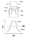
磁気抵抗素子を用いた磁気検出方式による検出信号について説明する。図5に示されるように、保持部107は、検出対象である突起部201に対して所定のギャップを持って配置される。そして、保持部107に対して突起部201が移動すると、突起部201の移動方向の中心で検出信号が最大となる。ギャップが大きくなると検出信号の振幅が小さくなり、ギャップが小さくなると検出信号の振幅が大きくなる。このような検出信号に対して閾値を設定することで突起部201の位置を検出することができる。
A detection signal by a magnetic detection method using a magnetoresistive element will be described. As shown in FIG. 5, the holding
なお、図5では突起部201の移動と磁気検出素子による検出信号との関係のみを示している。後述するが、検出信号は複数の磁気抵抗素子の出力によって生成する。
Note that FIG. 5 shows only the relationship between the movement of the
上記の磁気抵抗素子を用いた磁気検出方式では、磁気ベクトルを検出する磁気抵抗素子は、ギャップのずれによる精度誤差をキャンセルできるメリットがある。また、センサチップ110に発生する応力の影響を低減あるいはキャンセルできるメリットがある。よって、高精度な検出が可能である。
In the magnetic detection method using the above-mentioned magnetoresistive element, the magnetoresistive element for detecting the magnetic vector has an advantage that the accuracy error due to the gap shift can be canceled. Further, there is an advantage that the influence of stress generated in the
次に、センサチップ110及び処理回路チップ109に構成された回路構成について説明する。図6に示されるように、ポジションセンサ100とコントローラ300とがハーネス400を介して電気的に接続されている。上述のように、モールドIC部105は3本のリード113〜115を有しているので、ハーネス400は3本の配線によって構成されている。
Next, the circuit configuration of the
コントローラ300は、例えばトランスミッションコントローラ(TCU)である。コントローラ300は、電源部301、制御部302、及びグランド部303を備えている。電源部301は、ポジションセンサ100に電源電圧を供給する回路部である。制御部302は、ポジションセンサ100から入力する出力信号に応じて予め決められた制御を行う回路部である。グランド部303はポジションセンサ100のグランド電圧を設定する回路部である。なお、コントローラ300は、電子制御装置(ECU)として構成されていても良い。
The
ポジションセンサ100は、検出部119及び信号処理部120を備えている。検出部119は、センサチップ110に設けられている。信号処理部120は、処理回路チップ109に設けられている。検出部119及び信号処理部120は、コントローラ300から供給される電源電圧及びグランド電圧に基づいて動作する。
The
検出部119は、第1磁気抵抗素子121及び第2磁気抵抗素子122を有している。第1磁気抵抗素子121は、突起部201の位置に対応した第1検出信号を出力するように構成されている。第2磁気抵抗素子122は、突起部201の位置に対応した第2検出信号を出力するように構成されている。
The
各磁気抵抗素子121、122は、突起部201の移動に伴って抵抗値が変化する第1磁気抵抗素子対、第2磁気抵抗素子対、及び第3磁気抵抗素子対の3つの素子対を有している。
Each of the
突起部201の移動方向において、第2磁気抵抗素子対が第1磁気抵抗素子対と第3磁気抵抗素子対との間に位置するように各々が配置されている。つまり、第2磁気抵抗素子対が第1磁気抵抗素子対と第3磁気抵抗素子対とに挟まれるように配置されている。そして、第2磁気抵抗素子対には磁石106の中心軸に沿ったバイアス磁界が印加される。一方、第1磁気抵抗素子対及び第3磁気抵抗素子対には磁石106の端部を巻き込むバイアス磁界が印加される。
In the moving direction of the
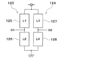
各磁気抵抗素子対は、電源とグランドとの間に2つの抵抗部が直列接続されたハーフブリッジ回路として構成されている。具体的には、図7に示されるように、第1磁気抵抗素子対は、第1磁気抵抗素子121の一部を構成する第1ハーフブリッジ回路123と、第2磁気抵抗素子122の一部を構成する第2ハーフブリッジ回路124と、によって構成されている。
Each pair of magnetoresistive elements is configured as a half bridge circuit in which two resistance sections are connected in series between a power source and a ground. Specifically, as shown in FIG. 7, the first magnetoresistive element pair includes a first half-
第1ハーフブリッジ回路123は、2つの抵抗部125、126(L1、L2)が直列接続されて構成されている。そして、各抵抗部125、126は、突起部201の移動に伴って2つの抵抗部125、126が磁界の影響を受けたときに抵抗値が変化する。したがって、第1ハーフブリッジ回路123は、当該抵抗値の変化に基づいて、2つの抵抗部125、126の中点の電圧G1を波形信号として出力する。この電圧G1は、2重系の第1系統の信号の1つである。
The first
第2ハーフブリッジ回路124は、2つの抵抗部127、128(L3、L4)が直列接続されている。そして、上記と同様に、第2ハーフブリッジ回路124は、各抵抗部127、128の抵抗値の変化に基づいて、2つの抵抗部127、128の中点の電圧G2を波形信号として出力する。この電圧G2は、2重系の第2系統の信号の1つである。
In the second
また、図8に示されるように、各ハーフブリッジ回路123、124は、配線パターンのバランスの中心が一致するように、センサチップ110の一面129に配置されている。なお、センサチップ110の一面129に配置されている場合とは、センサチップ110の一面129に直接配置されている場合だけでなく、一面129に形成された保護膜等の上に配置された場合も含まれる。
Further, as shown in FIG. 8, the
本実施形態では、第2ハーフブリッジ回路124の配線パターンは、センサチップ110の一面129において、第1ハーフブリッジ回路123の配線パターンを挟んだレイアウトである。具体的には、第1ハーフブリッジ回路123の各抵抗部125、126が隣り合うようにレイアウトされている。また、各抵抗部125、126の配線パターンは、例えば四角形の領域の中に形成されていると共に、配線の直線部分が図8の斜線に沿うように線対称に形成されている。これにより、第1ハーフブリッジ回路123の配線パターンのバランスの中心は、図8のP1となる。
In the present embodiment, the wiring pattern of the second
一方、第2ハーフブリッジ回路124の各抵抗部127、128は離れて位置するようにレイアウトされている。そして、抵抗部127と抵抗部128とに第1ハーフブリッジ回路123の各抵抗部125、126が挟まれている。各抵抗部127、128の配線パターンは、四角形の領域の中に形成されていると共に、配線の直線部分が図8の斜線に沿うように線対称に形成されている。これにより、第2ハーフブリッジ回路124の配線パターンのバランスの中心は、図8のP2となる。
On the other hand, the
つまり、センサチップ110の一面129の面内における第1ハーフブリッジ回路123の配線パターンのバランスの中心が、センサチップ110の一面129の面内における第2ハーフブリッジ回路124の配線パターンのバランスの中心と一致している。ここで、バランスの中心とは、レイアウトの中心、面積の重心、あるいは配線パターンの重心等のように、各抵抗部125、126や各抵抗部127、128のバランスが釣り合う位置である。したがって、第2ハーフブリッジ回路124のように、各抵抗部127、128が離れていても、各抵抗部127、128の位置とバランスの中心位置は関連しない。
That is, the center of the balance of the wiring patterns of the first
上記の構成によると、第1ハーフブリッジ回路123の各抵抗部125、126が受ける磁界方向変化の平均が電圧G1の変化となる。この電圧G1の変化は、第1ハーフブリッジ回路123の配線パターンのバランスの中心の磁界方向変化を反映した信号となる。同様に、第2ハーフブリッジ回路124の各抵抗部127、128が受ける磁界方向変化の平均が電圧G2の変化となる。この電圧G2の変化は、第2ハーフブリッジ回路124の配線パターンのバランスの中心の磁界方向変化を反映した信号となる。
According to the above configuration, the average of the changes in the magnetic field direction received by the
そして、第1磁気抵抗素子対は、突起部201の移動に伴って磁界の影響を受けたときの各抵抗部125、126及び各抵抗部127、128の抵抗値の変化を検出する。また、第1磁気抵抗素子対は、当該抵抗値の変化に基づいて、各ハーフブリッジ回路123、124の中点の電圧G1、G2を波形信号としてそれぞれ出力する。図9に示されるように、第1ハーフブリッジ回路123が出力する信号G1と、第2ハーフブリッジ回路124が出力する信号G2と、が全く同じ波形信号となる。すなわち、2重系の第1系統と第2系統との間に信号G1、G2のズレが全くない。
Then, the first magnetoresistive element pair detects a change in the resistance value of each of the
第2磁気抵抗素子対及び第3磁気抵抗素子対も上記と同様に2系統のハーフブリッジ回路123、124によって構成されている。すなわち、第2磁気抵抗素子対も、第1ハーフブリッジ回路123及び第2ハーフブリッジ回路124によって構成されている。第3磁気抵抗素子対も同じである。つまり、第1磁気抵抗素子121は、3つの素子対を有し、各素子対を構成する3つの第1ハーフブリッジ回路123を有している。第2磁気抵抗素子122についても同様に、3つの素子対を有し、各素子対を構成する3つの第2ハーフブリッジ回路124を有している。なお、図9ではセンサチップ110に第1磁気抵抗素子対のみが示されているが、実際には3つの素子対がセンサチップ110に設けられている。
Similarly to the above, the second magnetoresistive element pair and the third magnetoresistive element pair are also composed of two systems of
また、各磁気抵抗素子121、122は、第1〜第4オペアンプを備えている。各オペアンプは、磁気抵抗素子121、122毎に設けられている。
Further, each of the
第1磁気抵抗素子121について、第1磁気抵抗素子対の第1ハーフブリッジ回路123の中点電位をV1、第2磁気抵抗素子対の第1ハーフブリッジ回路123の中点電位をV2、第3磁気抵抗素子対の第1ハーフブリッジ回路123の中点電位をV3と定義する。
Regarding the first
第1オペアンプは、V1−V2を演算してその結果をR1として出力するように構成された差動増幅器である。また、第2オペアンプは、V2−V3を演算してその結果をR2として出力するように構成された差動増幅器である。 The first operational amplifier is a differential amplifier configured to calculate V1-V2 and output the result as R1. The second operational amplifier is a differential amplifier configured to calculate V2-V3 and output the result as R2.
第3オペアンプは、V1−V3を演算してその結果をS1として出力するように構成された差動増幅器である。例えば、信号S1は、シャフト200の突起部201の移動方向中心で振幅が最大となり、突起部201から離れた位置で振幅が最小となる波形の信号である。
The third operational amplifier is a differential amplifier configured to calculate V1-V3 and output the result as S1. For example, the signal S1 is a signal having a waveform in which the amplitude becomes maximum at the center of the moving direction of the
第4オペアンプは、第1オペアンプからR1(=V1−V2)を入力すると共に第2オペアンプからR2(=V2−V3)を入力し、R2−R1を演算してその結果をS2(=(V2−V3)−(V1−V2))として出力するように構成された差動増幅器である。このS2の信号は、シャフト200の突起部201の凹凸構造に対応した波形の信号である。例えば、信号S2は、シャフト200の突起部201の凹から凸に切り替わる一方のエッジ部分で振幅が最大となり、凸から凹に切り替わる他方のエッジ部分で振幅が最小となる波形の信号である。この信号S2は、信号S1に対して位相差を持った波形の信号である。第1磁気抵抗素子121は、信号S1及び信号S2を第1検出信号として信号処理部120に出力する。
The fourth operational amplifier inputs R1 (=V1-V2) from the first operational amplifier and R2 (=V2-V3) from the second operational amplifier, calculates R2-R1 and outputs the result to S2(=(V2 -V3)-(V1-V2)). The signal of S2 is a signal having a waveform corresponding to the uneven structure of the
第2磁気抵抗素子122についても上記と同様に、信号S1(=V1−V3)及び信号S2(=(V2−V3)−(V1−V2))をそれぞれ生成及び取得する。第2磁気抵抗素子122は、信号S1及び信号S2を第2検出信号として信号処理部120に出力する。
Similarly to the above, the
なお、各オペアンプは信号処理部120に設けられていても良い。すなわち、各検出信号は、信号処理部120によって取得されるように構成されていても良い。
Note that each operational amplifier may be provided in the
図6の信号処理部120は、検出部119から入力される信号を処理する回路部である。信号処理部120は、第1処理部130、第2処理部131、故障判定部132、及び出力回路部133を備えている。
The
第1処理部130は、第1磁気抵抗素子121から第1検出信号を入力し、第1検出信号に基づいて突起部201の位置を特定する。第2処理部131は、第2磁気抵抗素子122から第2検出信号を入力し、第2検出信号に基づいて突起部201の位置を特定する。このため、各処理部130、131は、検出信号に対して閾値を有している。
The first processing unit 130 receives the first detection signal from the first
そして、各処理部130、131は、検出信号である信号S1、S2と閾値とを比較する。各処理部130、131は、信号S1、S2が閾値よりも大きい場合をHiと判定し、信号S1、S2が閾値よりも小さい場合をLoと判定する。また、各処理部130、131は、信号S1、S2のHi/Loの組み合わせから、各磁気抵抗素子121、122がシャフト200のどの範囲を検出したのかを判定する。
Then, the
具体的には、図10に示されるように、信号S1がLo、信号S2がHiの場合、各磁気抵抗素子121、122はシャフト200のうち突起部201よりも図面左側の範囲を検出したことになる。つまり、各処理部130、131は、シャフト200の位置を特定したことになる。当該範囲の位置を特定した場合のシャフト200の状態を「状態A」とする。
Specifically, as shown in FIG. 10, when the signal S1 is Lo and the signal S2 is Hi, the
同様に、信号S1がHiの場合、各磁気抵抗素子121、122はシャフト200のうち突起部201の範囲を検出したことになる。この場合、信号S2のHi/Loは問わない。したがって、当該範囲の位置を特定した場合のシャフト200の状態を「状態B」とする。
Similarly, when the signal S1 is Hi, each of the
さらに、信号S1がLo、信号S2がLoの場合、各磁気抵抗素子121、122はシャフト200のうち突起部201よりも図面右側の範囲を検出したことになる。当該範囲の位置を特定した場合のシャフト200の状態を「状態C」とする。このように、各処理部130、131は、シャフト200の移動方向に沿った複数の範囲のいずれかの範囲の位置としてシャフト200の位置を特定する。
Further, when the signal S1 is Lo and the signal S2 is Lo, each of the
ここで、第1磁気抵抗素子121及び第1処理部130が第1系統を構成する。また、第2磁気抵抗素子122及び第2処理部131が第2系統を構成する。
Here, the first
なお、各処理部130、131は、複数の範囲にそれぞれ設定された離散的な値のうち特定した位置の範囲に対応した値の信号を故障判定部132に出力しても良い。離散的な値の信号は、例えば、電圧値が異なる電圧信号や、パルス幅が異なるパルス信号である。
Each of the
故障判定部132は、第1処理部130によって特定された位置と第2処理部131によって特定された位置とが一致するか否かを判定する回路部である。各処理部130、131によって特定された位置は、上記の状態A〜Cの種類である。したがって、故障判定部132は、各処理部130、131で特定された状態が一致するか否かを判定する。故障判定部132は、故障判定の結果を出力回路部133に出力する。
The failure determination unit 132 is a circuit unit that determines whether or not the position specified by the first processing unit 130 and the position specified by the
出力回路部133は、故障判定部132の判定結果に基づいて、コントローラ300に出力する信号を制御する回路部である。出力回路部133は、故障判定部132による判定が一致する場合は当該一致する位置に対応した位置信号を出力端子115に出力する。一方、出力回路部133は、故障判定部132による判定が不一致の場合は故障に対応した故障信号を出力端子115に出力する。以上が、本実施形態に係るポジションセンサ100の構成である。
The
ここで、比較例として、図11に示されるように、各系統が別々のセンサチップ110に設けられる構成がある。この構成では、一方のセンサチップ110に第1系統の第1ハーフブリッジ回路123が設けられる。第1ハーフブリッジ回路123の配線パターンのバランスの中心は、図11のP1となる。また、他方のセンサチップ110に第2系統の第2ハーフブリッジ回路124が設けられる。第2ハーフブリッジ回路124の配線パターンのバランスの中心は、図11のP2となる。なお、等価回路は図7と同じである。
Here, as a comparative example, as shown in FIG. 11, there is a configuration in which each system is provided in a
このように、各ハーフブリッジ回路123、124の配線パターンのバランスの中心が一致していない場合、図12に示されるように、各ハーフブリッジ回路123、124の電圧G1、G2に位相差が生じてしまう。
Thus, when the centers of the balance of the wiring patterns of the
別の比較例として、図13に示されるように、1つのセンサチップ110に各ハーフブリッジ回路123、124が設けられる場合もある。しかし、第1ハーフブリッジ回路123の各抵抗部125、126が隣同士にレイアウトされ、第2ハーフブリッジ回路124の各抵抗部127、128が隣同士にレイアウトされているので、各ハーフブリッジ回路123、124の配線パターンのバランスの中心が一致しない。したがって、この場合も、図14に示されるように、各ハーフブリッジ回路123、124の電圧G1、G2に位相差が生じてしまう。
As another comparative example, as shown in FIG. 13, one
図11〜図14に示された比較例では、信号の系統間誤差が発生し、系統間で位置検出誤差が発生する。このため、2重系でありながら、同じ位置を検出できない。 In the comparative example shown in FIGS. 11 to 14, an inter-system error of a signal occurs and a position detection error occurs between the systems. For this reason, the same position cannot be detected even though it is a dual system.
このような比較例に対し、本実施形態では各ハーフブリッジ回路123、124の配線パターンのバランスの中心が互いに一致しているので、各磁気抵抗素子121、122がシャフト200から受ける磁界の変化の平均が一致する。このため、各系統で同一の検出信号を生成することができる。したがって、検出部119が2重系に構成されていたとしても、検出位置の系統間誤差を無くすことができる。このように、検出信号の系統間誤差は発生せず、系統間で位置検出誤差は発生しないので、2重系の各系統で同じ位置を検出することができる。
In contrast to such a comparative example, in the present embodiment, since the center of the balance of the wiring patterns of the
変形例として、図15に示されるように、第1ハーフブリッジ回路123の各抵抗部125、126は、配線の直線部分が図15の斜線に沿うように同じ向きに形成されていても良い。第2ハーフブリッジ回路124の各抵抗部127、128についても同様である。
As a modified example, as shown in FIG. 15, the
変形例として、図16に示されるように、第1ハーフブリッジ回路123は電流源134によって動作する構成でも良い。この場合、第1ハーフブリッジ回路123の両端電圧G1が出力される。第2ハーフブリッジ回路124についても同様である。
As a modified example, as shown in FIG. 16, the first
変形例として、図17に示されるように、第1ハーフブリッジ回路123は4つの抵抗部125、126、135、136(L1〜L4)の直列接続として構成され、第2ハーフブリッジ回路124は4つの抵抗部127、128、137、138(L5〜L8)の直列接続として構成されていても良い。この場合、第1ハーフブリッジ回路123は、抵抗部126と抵抗部135との接続部の電圧G1を出力する。第2ハーフブリッジ回路124は、抵抗部128と抵抗部137との接続部の電圧G2を出力する。
As a modified example, as shown in FIG. 17, the first half-
この場合、図18に示されるように、第1ハーフブリッジ回路123の各抵抗部125、126、135、136は、十字状に配置される。例えば、抵抗部125(L1)の対角位置に抵抗部126(L2)が配置される。同様に、抵抗部135(L3)の対角位置に抵抗部136(L4)が配置される。これにより、抵抗部125、126の隣に抵抗部135、136が位置する。また、配線パターンの向きも十字状になっている。そして、4つの抵抗部125、126、135、136の配線パターンのバランスの中心は、図18のP1となる。
In this case, as shown in FIG. 18, the
一方、第2ハーフブリッジ回路124の各抵抗部127、128、137、138は、上記と同様に十字状に配置されるが、抵抗部127及び抵抗部138と抵抗部137と抵抗部128とが離れて位置するようにレイアウトされている。そして、4つの抵抗部127、128、137、138の配線パターンのバランスの中心は、図18のP2となり、第1ハーフブリッジ回路123の配線パターンのバランスの中心と一致する。このように、各ハーフブリッジ回路123、124の配線パターンを多数の分割することで、各抵抗部125〜128、135〜138がセンサチップ110から受ける応力を緩和あるいはキャンセルすることができる。なお、各ハーフブリッジ回路123、124をいくつの抵抗部で構成するかは適宜設計すれば良い。
On the other hand, the
変形例として、図19及び図20に示されるように、各ハーフブリッジ回路123、124の配線パターンは不均一に形成されていても良い。このような場合でも、各ハーフブリッジ回路123、124の配線パターンのバランスの中心が一致している。配線パターンが不均一の場合、配線パターンの面積重心を一致させるように設計すれば良い。また、図20に示されるように、一定の領域が設けられるように配線パターンが設計されることで、配線パターンの中にトランジスタ等の素子を配置することが可能になる。
As a modified example, as shown in FIGS. 19 and 20, the wiring patterns of the
変形例として、図21に示されるように、各ハーフブリッジ回路123、124の配線パターンは線対称に形成されていても良い。例えば、第1ハーフブリッジ回路123の各抵抗部125、126は広い領域に形成され、第2ハーフブリッジ回路124の各抵抗部127、128は狭い領域に形成されている。
As a modification, as shown in FIG. 21, the wiring patterns of the
変形例として、図22に示されるように、センサチップ110の一面129において、第1ハーフブリッジ回路123の配線パターンと、第2ハーフブリッジ回路124の配線パターンと、が混在して形成されていても良い。このような場合でも、各ハーフブリッジ回路123、124の配線パターンのバランスの中心が一致させることができる。
As a modified example, as shown in FIG. 22, on one
なお、本実施形態の記載と特許請求の範囲の記載との対応関係については、シャフト200が特許請求の範囲の「検出対象」に対応する。また、各磁気抵抗素子121、122が特許請求の範囲の「検出素子」に対応する。
Regarding the correspondence between the description of the present embodiment and the description of the claims, the
(第2実施形態)
本実施形態では、第1実施形態と異なる部分について説明する。図23及び図24に示されるように、第1ハーフブリッジ回路123及び第2ハーフブリッジ回路124は、センサチップ110の一面129に階層状に配置されている。本実施形態では、第1ハーフブリッジ回路123の配線パターンがセンサチップ110の一面129側に位置するように各ハーフブリッジ回路123、124の配線パターンが層状に設けられている。
(Second embodiment)
In the present embodiment, parts different from the first embodiment will be described. As shown in FIGS. 23 and 24, the first
具体的には、センサチップ110の一面129に第1ハーフブリッジ回路123の各抵抗部125、126が形成されている。センサチップ110の一面129には各抵抗部125、126を覆うように層間絶縁膜139が形成されている。また、層間絶縁膜139の上には、第2ハーフブリッジ回路124の各抵抗部127、128が形成されている。さらに、層間絶縁膜139の上には各抵抗部127、128を覆う保護膜140が形成されている。
Specifically, the
そして、抵抗部125の上に抵抗部127が位置し、抵抗部126の上に抵抗部128が位置している。このように、各ハーフブリッジ回路123、124の配線パターンが2層構造に形成されていたとしても、各ハーフブリッジ回路123、124の配線パターンのバランスの中心はセンサチップ110の一面129の面内で一致している。したがって、第1実施形態と同様の効果が得られる。
The
変形例として、第2ハーフブリッジ回路124の配線パターンがセンサチップ110の一面129側に位置するように、配線パターンが層状に設けられていても良い。
As a modified example, the wiring patterns of the second
(第3実施形態)
本実施形態では、第1、第2実施形態と異なる部分について説明する。ホール素子を用いた磁気検出方式を採用した場合、図25の平面模式図及び図26の断面模式図に示されるように、モールドIC部105は、保持部107に差し込まれて固定される。また、モールドIC部105は、リードフレーム108、ICチップ141、磁石142、及びモールド樹脂部111を有している。
(Third Embodiment)
In this embodiment, parts different from the first and second embodiments will be described. When the magnetic detection method using the Hall element is adopted, the
リードフレーム108のアイランド部112は、平面部が検出対象の移動方向に対して平行になるように配置されている。一方、各リード113〜115は、検出対象の移動方向に対して垂直になるように配置されている。グランド用のリード114がアイランド部112に直角に一体化されている。各リード113〜115の先端にはターミナル116がそれぞれ接続されている。
The
ICチップ141は、複数のホール素子と信号処理回路部とが形成されている。つまり、ホール素子を用いた磁気検出方式では1チップ構成になっている。磁石142は、アイランド部112のうちICチップ141とは反対側の面に固定されている。各リード113〜115とICチップ141とは、ワイヤ143を介して電気的に接続されている。モールド樹脂部111は、保持部107の中空部に固定される形状に成形されている。
The
ホール素子を用いた磁気検出方式による検出信号について説明する。図27に示されるように、例えば2つのホール素子(X、Y)が磁石142の上方に配置されている場合、保持部107に対して突起部201が移動すると、各ホール素子(X、Y)の位置に対応して各検出信号が最大となる。ギャップと検出信号の振幅との関係は磁気抵抗素子を用いた磁気検出方式と同じである。各検出信号に対して閾値を設定することで突起部201の位置を検出することができる。
A detection signal by the magnetic detection method using the Hall element will be described. As shown in FIG. 27, for example, when two Hall elements (X, Y) are arranged above the
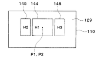
検出素子としてホール素子を採用した場合、図28に示されるように、3つのホール素子144〜146(H1〜H3)で2重系を構成することができる。ホール素子144が第1系統の信号を出力する。また、ホール素子144は、例えば四角形の領域の中に形成されている。これにより、ホール素子144のバランスの中心は、図28のP1となる。ホール素子144の出力h1を第1系統の信号G3とする。
When a Hall element is used as the detection element, as shown in FIG. 28, a double system can be configured with three
一方、ホール素子145、146が第2系統の信号を出力する。各ホール素子145、146は離れて位置するようにレイアウトされている。そして、各ホール素子145、146に第1系統のホール素子144が挟まれている。各ホール素子145、146は、四角形の領域の中に形成されている。これにより、各ホール素子145、146のバランスの中心は、図28のP2となる。ホール素子145の出力h2とホール素子146の出力h3との和(h2+h3)を第2系統の信号G4とする。
On the other hand, the
上記の構成によると、第1実施形態と同様に、図29に示されるように、第1系統の信号G3と第2系統の信号G4とが全く同じ波形信号となる。このように、ホール素子144〜146を用いても、2重系の第1系統と第2系統との間に信号G3、G4のズレが全くない。
According to the above configuration, as in the first embodiment, as shown in FIG. 29, the first system signal G3 and the second system signal G4 have exactly the same waveform signal. Thus, even if the
そして、図28に示されたホール素子144〜146を1つの検出素子とすると、図30に示されるように、3つの検出素子147〜149がそれぞれ2重系を構成している。この場合、検出素子147の出力をV4、検出素子148の出力をV5、検出素子149の出力をV6とすると、検出部119は、信号S3(=V5)と、信号S4(=V4−V6)と、を生成し、検出信号として信号処理部120に出力する。2重系であるので、検出部119は、第1系統の信号S3、S4を第1検出信号とし、第2系統の信号S3、S4を第2検出信号として信号処理部120に出力する。図30では1つの系統を示している。そして、第1実施形態の図10の場合と同様に、状態判定が行われる。
Then, assuming that the
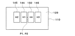
変形例として、図31に示されるように、4つのホール素子144〜146、150(H1〜H4)で2重系が構成されても良い。この場合の各ホール素子144〜146、150の配置は図8と同じである。
As a modification, as shown in FIG. 31, four
なお、本実施形態の記載と特許請求の範囲の記載との対応関係については、第1系統を構成するホール素子144、150が特許請求の範囲の「第1検出素子」に対応し、第2系統を構成するホール素子145、146が特許請求の範囲の「第2検出素子」に対応する。
Regarding the correspondence relationship between the description of the present embodiment and the description of the claims, the
(他の実施形態)
上記各実施形態で示されたポジションセンサ100の構成は一例であり、上記で示した構成に限定されることなく、本発明を実現できる他の構成とすることもできる。例えば、ポジションセンサ100の用途は車両用に限られず、可動部品の位置を検出するものとして産業用ロボットや製造設備等にも広く利用できる。
(Other embodiments)
The configuration of the
110 センサチップ
119 検出部
121、122 磁気抵抗素子
123、124 ハーフブリッジ回路
129 一面
144〜146、150 ホール素子
110
Claims (3)
前記検出部から入力される信号を処理する信号処理部(120)と、
を備え、
前記第1検出素子は、第1ハーフブリッジ回路(123)を構成し、検出対象(200)から受ける磁界の変化に基づいて、前記検出対象の位置に対応した第1検出信号を出力し、
前記第2検出素子は、第2ハーフブリッジ回路(124)を構成し、前記検出対象から受ける磁界の変化に基づいて、前記検出対象の位置に対応した第2検出信号を出力し、
さらに、前記一面の面内における前記第1検出素子のバランスの中心が、前記一面の面内における前記第2検出素子のバランスの中心と一致しており、
前記一面において、前記第1ハーフブリッジ回路の配線パターンと、前記第2ハーフブリッジ回路の配線パターンと、が同一領域内に混在して形成されているポジションセンサ。 A sensor chip (110) having one surface (129), first detection elements (121, 144, 150) provided on the sensor chip, and second detection elements (122, 145, 146) provided on the sensor chip. ) And a detection unit (119) having
A signal processing unit (120) for processing a signal input from the detection unit;
Equipped with
The first detection element constitutes a first half bridge circuit (123), and outputs a first detection signal corresponding to the position of the detection target based on a change in a magnetic field received from the detection target (200),
The second detection element constitutes a second half bridge circuit (124), and outputs a second detection signal corresponding to the position of the detection target based on a change in the magnetic field received from the detection target,
Further, the center of balance of the first detection element in the plane of the one surface matches the center of balance of the second detection element in the plane of the one surface ,
A position sensor in which the wiring pattern of the first half-bridge circuit and the wiring pattern of the second half-bridge circuit are formed in a mixed manner in the same area on the one surface .
前記検出部から入力される信号を処理する信号処理部(120)と、
を備え、
前記第1検出素子は、第1ハーフブリッジ回路(123)を構成し、検出対象(200)から受ける磁界の変化に基づいて、前記検出対象の位置に対応した第1検出信号を出力し、
前記第2検出素子は、第2ハーフブリッジ回路(124)を構成し、前記検出対象から受ける磁界の変化に基づいて、前記検出対象の位置に対応した第2検出信号を出力し、
さらに、前記一面の面内における前記第1検出素子のバランスの中心が、前記一面の面内における前記第2検出素子のバランスの中心と一致しており、
前記第1ハーフブリッジ回路及び前記第2ハーフブリッジ回路は、前記センサチップの前記一面の垂直方向に階層状に配置され、前記第1ハーフブリッジ回路及び前記第2ハーフブリッジ回路のうちのいずれか一方の配線パターンが前記センサチップの前記一面側に位置するように前記各ハーフブリッジ回路の配線パターンが層状に設けられているポジションセンサ。 A sensor chip (110) having one surface (129), first detection elements (121, 144, 150) provided on the sensor chip, and second detection elements (122, 145, 146) provided on the sensor chip. ) And a detection unit (119) having
A signal processing unit (120) for processing a signal input from the detection unit;
Equipped with
The first detection element constitutes a first half bridge circuit (123), and outputs a first detection signal corresponding to the position of the detection target based on a change in a magnetic field received from the detection target (200),
The second detection element constitutes a second half bridge circuit (124), and outputs a second detection signal corresponding to the position of the detection target based on a change in the magnetic field received from the detection target,
Furthermore, the center of balance of the first detection element in the plane of the one surface matches the center of balance of the second detection element in the plane of the one surface,
The first half-bridge circuit and the second half-bridge circuit are arranged in a hierarchy in a vertical direction of the one surface of the sensor chip , and one of the first half-bridge circuit and the second half-bridge circuit is arranged. The position sensor in which the wiring patterns of the respective half bridge circuits are provided in layers so that the wiring pattern is located on the one surface side of the sensor chip.
Priority Applications (5)
| Application Number | Priority Date | Filing Date | Title |
|---|---|---|---|
| JP2017118778A JP6743770B2 (en) | 2017-06-16 | 2017-06-16 | Position sensor |
| CN201880039451.2A CN110741230B (en) | 2017-06-16 | 2018-05-17 | Position sensor |
| DE112018003054.7T DE112018003054T5 (en) | 2017-06-16 | 2018-05-17 | Position sensor |
| PCT/JP2018/019060 WO2018230243A1 (en) | 2017-06-16 | 2018-05-17 | Position sensor |
| US16/697,902 US11733063B2 (en) | 2017-06-16 | 2019-11-27 | Position sensor |
Applications Claiming Priority (1)
| Application Number | Priority Date | Filing Date | Title |
|---|---|---|---|
| JP2017118778A JP6743770B2 (en) | 2017-06-16 | 2017-06-16 | Position sensor |
Publications (3)
| Publication Number | Publication Date |
|---|---|
| JP2019002836A JP2019002836A (en) | 2019-01-10 |
| JP2019002836A5 JP2019002836A5 (en) | 2019-06-20 |
| JP6743770B2 true JP6743770B2 (en) | 2020-08-19 |
Family
ID=64660839
Family Applications (1)
| Application Number | Title | Priority Date | Filing Date |
|---|---|---|---|
| JP2017118778A Active JP6743770B2 (en) | 2017-06-16 | 2017-06-16 | Position sensor |
Country Status (5)
| Country | Link |
|---|---|
| US (1) | US11733063B2 (en) |
| JP (1) | JP6743770B2 (en) |
| CN (1) | CN110741230B (en) |
| DE (1) | DE112018003054T5 (en) |
| WO (1) | WO2018230243A1 (en) |
Families Citing this family (4)
| Publication number | Priority date | Publication date | Assignee | Title |
|---|---|---|---|---|
| JP2019002469A (en) | 2017-06-14 | 2019-01-10 | 株式会社デンソー | Position sensor |
| JP6791033B2 (en) | 2017-06-16 | 2020-11-25 | 株式会社デンソー | Position sensor |
| US11686788B2 (en) | 2021-07-08 | 2023-06-27 | Tdk Corporation | Magnetic sensor device and magnetic sensor system |
| CN113418440A (en) * | 2021-08-05 | 2021-09-21 | 重庆编福科技有限公司 | Non-contact position detection method |
Family Cites Families (18)
| Publication number | Priority date | Publication date | Assignee | Title |
|---|---|---|---|---|
| US6452381B1 (en) * | 1997-11-28 | 2002-09-17 | Denso Corporation | Magnetoresistive type position detecting device |
| JP4293037B2 (en) * | 2004-04-13 | 2009-07-08 | 株式会社デンソー | Rotation detector |
| JP4466355B2 (en) | 2004-06-23 | 2010-05-26 | 株式会社デンソー | Rotation detector |
| JP2006300779A (en) | 2005-04-21 | 2006-11-02 | Denso Corp | Rotation detector |
| JP2009014454A (en) * | 2007-07-03 | 2009-01-22 | Tokai Rika Co Ltd | Position detection device |
| JP5014968B2 (en) * | 2007-12-07 | 2012-08-29 | 株式会社東海理化電機製作所 | Position sensor |
| EP2634592B1 (en) * | 2009-07-22 | 2015-01-14 | Allegro Microsystems, LLC | Circuits and methods for generating a diagnostic mode of operation in a magnetic field sensor |
| JP5249156B2 (en) | 2009-08-21 | 2013-07-31 | 株式会社東海理化電機製作所 | Sensor pattern arrangement structure of multi-system magnetic sensor and manufacturing method thereof |
| CN102298126B (en) * | 2011-01-17 | 2013-03-13 | 江苏多维科技有限公司 | Independent packaged bridge-type magnetic-field sensor |
| JP6064816B2 (en) * | 2013-07-17 | 2017-01-25 | 株式会社デンソー | Rotation sensor |
| JP2015108527A (en) | 2013-12-03 | 2015-06-11 | 株式会社東海理化電機製作所 | Magnetic sensor |
| JP2015129700A (en) | 2014-01-08 | 2015-07-16 | アルプス電気株式会社 | Magnetic field rotation detection sensor and magnetic encoder |
| US9719806B2 (en) | 2014-10-31 | 2017-08-01 | Allegro Microsystems, Llc | Magnetic field sensor for sensing a movement of a ferromagnetic target object |
| CN105890507B (en) * | 2015-01-08 | 2019-04-16 | 中国人民解放军军械工程学院 | A kind of localization method of giant magnetic impedance sensor to magnetic target in plane |
| US10012518B2 (en) * | 2016-06-08 | 2018-07-03 | Allegro Microsystems, Llc | Magnetic field sensor for sensing a proximity of an object |
| JP2019002469A (en) | 2017-06-14 | 2019-01-10 | 株式会社デンソー | Position sensor |
| JP6787260B2 (en) | 2017-06-14 | 2020-11-18 | 株式会社デンソー | Position sensor |
| JP6791033B2 (en) | 2017-06-16 | 2020-11-25 | 株式会社デンソー | Position sensor |
-
2017
- 2017-06-16 JP JP2017118778A patent/JP6743770B2/en active Active
-
2018
- 2018-05-17 CN CN201880039451.2A patent/CN110741230B/en active Active
- 2018-05-17 WO PCT/JP2018/019060 patent/WO2018230243A1/en active Application Filing
- 2018-05-17 DE DE112018003054.7T patent/DE112018003054T5/en active Pending
-
2019
- 2019-11-27 US US16/697,902 patent/US11733063B2/en active Active
Also Published As
| Publication number | Publication date |
|---|---|
| CN110741230B (en) | 2023-01-17 |
| CN110741230A (en) | 2020-01-31 |
| WO2018230243A1 (en) | 2018-12-20 |
| DE112018003054T5 (en) | 2020-03-05 |
| JP2019002836A (en) | 2019-01-10 |
| US20200096368A1 (en) | 2020-03-26 |
| US11733063B2 (en) | 2023-08-22 |
Similar Documents
| Publication | Publication Date | Title |
|---|---|---|
| JP6743770B2 (en) | Position sensor | |
| JP6033529B2 (en) | Detection device and current sensor | |
| US9297635B2 (en) | Magnetic sensor system including two detection circuits | |
| CN110741231B (en) | Position sensor | |
| WO2018230087A1 (en) | Position sensor | |
| CN107561312A (en) | For determining magnetic sensor device and method of the magnetic assembly around the direction of rotation of rotary shaft | |
| US20200072593A1 (en) | Position sensor | |
| WO2013171977A1 (en) | Bridge circuit and magnetic sensor comprising same | |
| JP2015179043A (en) | current sensor | |
| US10921388B2 (en) | Magnetic sensor with three detection units | |
| WO2023053792A1 (en) | Electric current sensor, method for correcting same, and method for correcting plurality of electric current sensors | |
| JP7119633B2 (en) | magnetic sensor | |
| JP5128416B2 (en) | Magnetic sensor device | |
| WO2014147996A1 (en) | Current sensor | |
| WO2021084801A1 (en) | Current sensor | |
| JP7043888B2 (en) | Linear position sensor | |
| US11047926B2 (en) | Magnetic sensor | |
| JP2016115240A (en) | Multiplication circuit and power sensor including the same | |
| JP7225694B2 (en) | magnetic sensor | |
| WO2021140724A1 (en) | Position detection device | |
| US9869730B2 (en) | Magnetic detection apparatus | |
| WO2019167440A1 (en) | Linear position sensor |
Legal Events
| Date | Code | Title | Description |
|---|---|---|---|
| A521 | Request for written amendment filed |
Free format text: JAPANESE INTERMEDIATE CODE: A523 Effective date: 20190520 |
|
| A621 | Written request for application examination |
Free format text: JAPANESE INTERMEDIATE CODE: A621 Effective date: 20190711 |
|
| A131 | Notification of reasons for refusal |
Free format text: JAPANESE INTERMEDIATE CODE: A131 Effective date: 20200421 |
|
| A521 | Request for written amendment filed |
Free format text: JAPANESE INTERMEDIATE CODE: A523 Effective date: 20200519 |
|
| TRDD | Decision of grant or rejection written | ||
| A01 | Written decision to grant a patent or to grant a registration (utility model) |
Free format text: JAPANESE INTERMEDIATE CODE: A01 Effective date: 20200630 |
|
| A61 | First payment of annual fees (during grant procedure) |
Free format text: JAPANESE INTERMEDIATE CODE: A61 Effective date: 20200713 |
|
| R151 | Written notification of patent or utility model registration |
Ref document number: 6743770 Country of ref document: JP Free format text: JAPANESE INTERMEDIATE CODE: R151 |
|
| R250 | Receipt of annual fees |
Free format text: JAPANESE INTERMEDIATE CODE: R250 |
|
| R250 | Receipt of annual fees |
Free format text: JAPANESE INTERMEDIATE CODE: R250 |