EP3190401B1 - Inspection device and inspection method - Google Patents
Inspection device and inspection method Download PDFInfo
- Publication number
- EP3190401B1 EP3190401B1 EP15838785.2A EP15838785A EP3190401B1 EP 3190401 B1 EP3190401 B1 EP 3190401B1 EP 15838785 A EP15838785 A EP 15838785A EP 3190401 B1 EP3190401 B1 EP 3190401B1
- Authority
- EP
- European Patent Office
- Prior art keywords
- area
- image
- picked
- defect candidate
- light source
- Prior art date
- Legal status (The legal status is an assumption and is not a legal conclusion. Google has not performed a legal analysis and makes no representation as to the accuracy of the status listed.)
- Active
Links
- 238000007689 inspection Methods 0.000 title claims description 53
- 238000000034 method Methods 0.000 title claims description 18
- 230000007547 defect Effects 0.000 claims description 214
- 238000001514 detection method Methods 0.000 claims description 20
- 230000001678 irradiating effect Effects 0.000 claims description 15
- 238000003384 imaging method Methods 0.000 description 5
- 239000002184 metal Substances 0.000 description 5
- 230000003287 optical effect Effects 0.000 description 5
- 238000001914 filtration Methods 0.000 description 4
- 229910000679 solder Inorganic materials 0.000 description 4
- 238000005266 casting Methods 0.000 description 2
- 239000002131 composite material Substances 0.000 description 2
- 238000010586 diagram Methods 0.000 description 2
- 238000011156 evaluation Methods 0.000 description 2
- 238000005242 forging Methods 0.000 description 2
- 238000005286 illumination Methods 0.000 description 2
- 238000004519 manufacturing process Methods 0.000 description 2
- 238000005422 blasting Methods 0.000 description 1
- 230000000295 complement effect Effects 0.000 description 1
- 230000002950 deficient Effects 0.000 description 1
- 230000005484 gravity Effects 0.000 description 1
- 239000000463 material Substances 0.000 description 1
- 229910044991 metal oxide Inorganic materials 0.000 description 1
- 150000004706 metal oxides Chemical class 0.000 description 1
- 238000012986 modification Methods 0.000 description 1
- 230000004048 modification Effects 0.000 description 1
- 239000004065 semiconductor Substances 0.000 description 1
- 238000004381 surface treatment Methods 0.000 description 1
- 238000011179 visual inspection Methods 0.000 description 1
Images


Classifications
-
- G—PHYSICS
- G01—MEASURING; TESTING
- G01N—INVESTIGATING OR ANALYSING MATERIALS BY DETERMINING THEIR CHEMICAL OR PHYSICAL PROPERTIES
- G01N21/00—Investigating or analysing materials by the use of optical means, i.e. using sub-millimetre waves, infrared, visible or ultraviolet light
- G01N21/84—Systems specially adapted for particular applications
- G01N21/88—Investigating the presence of flaws or contamination
- G01N21/95—Investigating the presence of flaws or contamination characterised by the material or shape of the object to be examined
-
- G—PHYSICS
- G01—MEASURING; TESTING
- G01N—INVESTIGATING OR ANALYSING MATERIALS BY DETERMINING THEIR CHEMICAL OR PHYSICAL PROPERTIES
- G01N21/00—Investigating or analysing materials by the use of optical means, i.e. using sub-millimetre waves, infrared, visible or ultraviolet light
- G01N21/84—Systems specially adapted for particular applications
- G01N21/88—Investigating the presence of flaws or contamination
- G01N21/8806—Specially adapted optical and illumination features
-
- G—PHYSICS
- G01—MEASURING; TESTING
- G01N—INVESTIGATING OR ANALYSING MATERIALS BY DETERMINING THEIR CHEMICAL OR PHYSICAL PROPERTIES
- G01N21/00—Investigating or analysing materials by the use of optical means, i.e. using sub-millimetre waves, infrared, visible or ultraviolet light
- G01N21/84—Systems specially adapted for particular applications
- G01N21/88—Investigating the presence of flaws or contamination
- G01N21/8851—Scan or image signal processing specially adapted therefor, e.g. for scan signal adjustment, for detecting different kinds of defects, for compensating for structures, markings, edges
-
- G—PHYSICS
- G01—MEASURING; TESTING
- G01N—INVESTIGATING OR ANALYSING MATERIALS BY DETERMINING THEIR CHEMICAL OR PHYSICAL PROPERTIES
- G01N21/00—Investigating or analysing materials by the use of optical means, i.e. using sub-millimetre waves, infrared, visible or ultraviolet light
- G01N21/84—Systems specially adapted for particular applications
- G01N21/88—Investigating the presence of flaws or contamination
- G01N21/95—Investigating the presence of flaws or contamination characterised by the material or shape of the object to be examined
- G01N21/956—Inspecting patterns on the surface of objects
- G01N21/95607—Inspecting patterns on the surface of objects using a comparative method
-
- G—PHYSICS
- G01—MEASURING; TESTING
- G01N—INVESTIGATING OR ANALYSING MATERIALS BY DETERMINING THEIR CHEMICAL OR PHYSICAL PROPERTIES
- G01N21/00—Investigating or analysing materials by the use of optical means, i.e. using sub-millimetre waves, infrared, visible or ultraviolet light
- G01N21/84—Systems specially adapted for particular applications
- G01N21/88—Investigating the presence of flaws or contamination
- G01N21/95—Investigating the presence of flaws or contamination characterised by the material or shape of the object to be examined
- G01N21/956—Inspecting patterns on the surface of objects
- G01N21/95684—Patterns showing highly reflecting parts, e.g. metallic elements
-
- G—PHYSICS
- G06—COMPUTING; CALCULATING OR COUNTING
- G06T—IMAGE DATA PROCESSING OR GENERATION, IN GENERAL
- G06T7/00—Image analysis
- G06T7/0002—Inspection of images, e.g. flaw detection
- G06T7/0004—Industrial image inspection
- G06T7/001—Industrial image inspection using an image reference approach
-
- G—PHYSICS
- G01—MEASURING; TESTING
- G01N—INVESTIGATING OR ANALYSING MATERIALS BY DETERMINING THEIR CHEMICAL OR PHYSICAL PROPERTIES
- G01N21/00—Investigating or analysing materials by the use of optical means, i.e. using sub-millimetre waves, infrared, visible or ultraviolet light
- G01N21/84—Systems specially adapted for particular applications
- G01N21/88—Investigating the presence of flaws or contamination
- G01N21/8806—Specially adapted optical and illumination features
- G01N2021/8812—Diffuse illumination, e.g. "sky"
- G01N2021/8816—Diffuse illumination, e.g. "sky" by using multiple sources, e.g. LEDs
-
- G—PHYSICS
- G01—MEASURING; TESTING
- G01N—INVESTIGATING OR ANALYSING MATERIALS BY DETERMINING THEIR CHEMICAL OR PHYSICAL PROPERTIES
- G01N21/00—Investigating or analysing materials by the use of optical means, i.e. using sub-millimetre waves, infrared, visible or ultraviolet light
- G01N21/84—Systems specially adapted for particular applications
- G01N21/88—Investigating the presence of flaws or contamination
- G01N21/8851—Scan or image signal processing specially adapted therefor, e.g. for scan signal adjustment, for detecting different kinds of defects, for compensating for structures, markings, edges
- G01N2021/8854—Grading and classifying of flaws
- G01N2021/8867—Grading and classifying of flaws using sequentially two or more inspection runs, e.g. coarse and fine, or detecting then analysing
-
- G—PHYSICS
- G01—MEASURING; TESTING
- G01N—INVESTIGATING OR ANALYSING MATERIALS BY DETERMINING THEIR CHEMICAL OR PHYSICAL PROPERTIES
- G01N21/00—Investigating or analysing materials by the use of optical means, i.e. using sub-millimetre waves, infrared, visible or ultraviolet light
- G01N21/84—Systems specially adapted for particular applications
- G01N21/88—Investigating the presence of flaws or contamination
- G01N21/8851—Scan or image signal processing specially adapted therefor, e.g. for scan signal adjustment, for detecting different kinds of defects, for compensating for structures, markings, edges
- G01N2021/8887—Scan or image signal processing specially adapted therefor, e.g. for scan signal adjustment, for detecting different kinds of defects, for compensating for structures, markings, edges based on image processing techniques
-
- G—PHYSICS
- G01—MEASURING; TESTING
- G01N—INVESTIGATING OR ANALYSING MATERIALS BY DETERMINING THEIR CHEMICAL OR PHYSICAL PROPERTIES
- G01N2201/00—Features of devices classified in G01N21/00
- G01N2201/06—Illumination; Optics
- G01N2201/062—LED's
-
- G—PHYSICS
- G06—COMPUTING; CALCULATING OR COUNTING
- G06T—IMAGE DATA PROCESSING OR GENERATION, IN GENERAL
- G06T2207/00—Indexing scheme for image analysis or image enhancement
- G06T2207/10—Image acquisition modality
- G06T2207/10141—Special mode during image acquisition
- G06T2207/10152—Varying illumination
Definitions
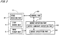
- the inspection apparatus further includes a control part sequentially using each of the plurality of light source parts as the first lighting part, to cause the image pickup part to acquire a plurality of first picked-up images, and in the inspection apparatus, the defect candidate detection part compares the plurality of first picked-up images with a plurality of first reference images corresponding to the plurality of first picked-up images, respectively, to generate a plurality of first defect candidate images each representing a first defect candidate area, and the defect specifying part specifies an overlapping area in the first defect candidate area represented by each first defect candidate image and the second defect candidate area, as a defect area in the object area. More preferably, the number of the plurality of light source parts is not less than 3.
Applications Claiming Priority (2)
| Application Number | Priority Date | Filing Date | Title |
|---|---|---|---|
| JP2014181054A JP6370177B2 (ja) | 2014-09-05 | 2014-09-05 | 検査装置および検査方法 |
| PCT/JP2015/062872 WO2016035381A1 (ja) | 2014-09-05 | 2015-04-28 | 検査装置および検査方法 |
Publications (3)
| Publication Number | Publication Date |
|---|---|
| EP3190401A1 EP3190401A1 (en) | 2017-07-12 |
| EP3190401A4 EP3190401A4 (en) | 2018-05-09 |
| EP3190401B1 true EP3190401B1 (en) | 2021-11-24 |
Family
ID=55439455
Family Applications (1)
| Application Number | Title | Priority Date | Filing Date |
|---|---|---|---|
| EP15838785.2A Active EP3190401B1 (en) | 2014-09-05 | 2015-04-28 | Inspection device and inspection method |
Country Status (7)
| Country | Link |
|---|---|
| US (1) | US10705029B2 (zh) |
| EP (1) | EP3190401B1 (zh) |
| JP (1) | JP6370177B2 (zh) |
| KR (1) | KR101931456B1 (zh) |
| CN (1) | CN106796179B (zh) |
| TW (1) | TWI580951B (zh) |
| WO (1) | WO2016035381A1 (zh) |
Families Citing this family (51)
| Publication number | Priority date | Publication date | Assignee | Title |
|---|---|---|---|---|
| US10268906B2 (en) | 2014-10-24 | 2019-04-23 | Magik Eye Inc. | Distance sensor with directional projection beams |
| EP3295119A4 (en) | 2015-05-10 | 2019-04-10 | Magik Eye Inc. | DISTANCE SENSOR |
| US10488192B2 (en) * | 2015-05-10 | 2019-11-26 | Magik Eye Inc. | Distance sensor projecting parallel patterns |
| US10448551B2 (en) * | 2015-05-25 | 2019-10-15 | Fuji Corporation | Component mounter |
| US10068326B2 (en) * | 2016-03-18 | 2018-09-04 | Siemens Energy, Inc. | System and method for enhancing visual inspection of an object |
| JP6917757B2 (ja) * | 2016-06-15 | 2021-08-11 | 株式会社Screenホールディングス | 外観検査装置、表面処理システム、外観検査方法、プログラム、および投射材交換判断方法 |
| JP6832650B2 (ja) * | 2016-08-18 | 2021-02-24 | 株式会社Screenホールディングス | 検査装置および検査方法 |
| DE102016011497B4 (de) * | 2016-09-21 | 2019-01-24 | Mühlbauer Gmbh & Co. Kg | Optische Untersuchungseinrichtung und optisches Untersuchungsverfahren mit sichtbarem und infrarotem Licht für Halbleiterbauteile |
| JP6499139B2 (ja) * | 2016-10-14 | 2019-04-10 | 矢崎総業株式会社 | 検査装置 |
| US10337860B2 (en) | 2016-12-07 | 2019-07-02 | Magik Eye Inc. | Distance sensor including adjustable focus imaging sensor |
| JP2018159650A (ja) | 2017-03-23 | 2018-10-11 | 株式会社Screenホールディングス | 照明装置、照明方法および撮像装置 |
| KR20200012838A (ko) * | 2017-05-26 | 2020-02-05 | 신토고교 가부시키가이샤 | 검사 장치 및 주조 시스템 |
| JP6679538B2 (ja) | 2017-06-05 | 2020-04-15 | 株式会社Screenホールディングス | 検査装置および検査方法 |
| JP7254324B2 (ja) * | 2017-06-05 | 2023-04-10 | 学校法人梅村学園 | 画像検査システムの性能調整のための検査用画像を生成する画像生成装置及び画像生成方法 |
| JP2020537237A (ja) | 2017-10-08 | 2020-12-17 | マジック アイ インコーポレイテッド | 縦グリッドパターンを使用した距離測定 |
| JP2020537242A (ja) * | 2017-10-08 | 2020-12-17 | マジック アイ インコーポレイテッド | 複数の可動センサを含むセンサシステムの校正 |
| US10679076B2 (en) | 2017-10-22 | 2020-06-09 | Magik Eye Inc. | Adjusting the projection system of a distance sensor to optimize a beam layout |
| CN108132264A (zh) * | 2017-12-19 | 2018-06-08 | 江苏伊莱尔电力科技有限公司 | 一种滤波器成品缺陷检测方法法 |
| CN109961455B (zh) * | 2017-12-22 | 2022-03-04 | 杭州萤石软件有限公司 | 一种目标检测方法及装置 |
| WO2019138930A1 (ja) * | 2018-01-15 | 2019-07-18 | 株式会社Screenホールディングス | 錠剤検査方法および錠剤検査装置 |
| JP7083646B2 (ja) * | 2018-01-15 | 2022-06-13 | 株式会社Screenホールディングス | 錠剤検査方法および錠剤検査装置 |
| JP7113627B2 (ja) | 2018-02-05 | 2022-08-05 | 株式会社Screenホールディングス | 画像取得装置、画像取得方法および検査装置 |
| JP7170400B2 (ja) * | 2018-02-14 | 2022-11-14 | 株式会社Screenホールディングス | 検査装置、検査方法、錠剤印刷装置および錠剤印刷方法 |
| JP6598898B2 (ja) * | 2018-02-27 | 2019-10-30 | 株式会社Screenホールディングス | 芯ズレ検出装置および芯ズレ検出方法 |
| JP7073785B2 (ja) * | 2018-03-05 | 2022-05-24 | オムロン株式会社 | 画像検査装置、画像検査方法及び画像検査プログラム |
| EP3769121A4 (en) | 2018-03-20 | 2021-12-29 | Magik Eye Inc. | Distance measurement using projection patterns of varying densities |
| US10931883B2 (en) | 2018-03-20 | 2021-02-23 | Magik Eye Inc. | Adjusting camera exposure for three-dimensional depth sensing and two-dimensional imaging |
| JP7076280B2 (ja) * | 2018-04-27 | 2022-05-27 | 日立造船株式会社 | 測定方法および測定装置 |
| WO2019236563A1 (en) | 2018-06-06 | 2019-12-12 | Magik Eye Inc. | Distance measurement using high density projection patterns |
| JP7188930B2 (ja) | 2018-07-27 | 2022-12-13 | 株式会社Screenホールディングス | 刻印検査装置、刻印検査方法および物品検査装置 |
| CN108896566A (zh) * | 2018-07-27 | 2018-11-27 | 佛山市坦斯盯科技有限公司 | 一种aoi相机及光源模组 |
| KR102112053B1 (ko) * | 2018-08-01 | 2020-05-18 | 주식회사 뷰온 | 이미지 센서를 이용한 표면결함 검사장치 및 검사방법 |
| WO2020033169A1 (en) * | 2018-08-07 | 2020-02-13 | Magik Eye Inc. | Baffles for three-dimensional sensors having spherical fields of view |
| JP7223840B2 (ja) * | 2018-09-20 | 2023-02-16 | シーメンス・ヘルスケア・ダイアグノスティックス・インコーポレイテッド | ビジョンベース検査システムの光学構成要素の自律診断検証のためのシステム、方法、および装置 |
| JP7386400B2 (ja) * | 2018-10-25 | 2023-11-27 | パナソニックIpマネジメント株式会社 | 照明制御装置、照明制御システム、及び照明制御方法 |
| JP6956063B2 (ja) * | 2018-12-07 | 2021-10-27 | ファナック株式会社 | 加工品の表面損傷検査システム |
| EP3911920A4 (en) | 2019-01-20 | 2022-10-19 | Magik Eye Inc. | THREE-DIMENSIONAL SENSOR INCLUDING A BANDPASS FILTER WITH MULTIPLE PASSBANDS |
| US11474209B2 (en) | 2019-03-25 | 2022-10-18 | Magik Eye Inc. | Distance measurement using high density projection patterns |
| CN114073075A (zh) | 2019-05-12 | 2022-02-18 | 魔眼公司 | 将三维深度图数据映射到二维图像上 |
| KR20220043219A (ko) * | 2019-09-13 | 2022-04-05 | 코니카 미놀타 가부시키가이샤 | 표면 결함 판별 장치, 외관 검사 장치 및 프로그램 |
| JP7236612B2 (ja) * | 2019-09-27 | 2023-03-10 | パナソニックIpマネジメント株式会社 | 検査方法、プログラム、及び、検査システム |
| WO2021113135A1 (en) | 2019-12-01 | 2021-06-10 | Magik Eye Inc. | Enhancing triangulation-based three-dimensional distance measurements with time of flight information |
| JP6755603B1 (ja) * | 2019-12-25 | 2020-09-16 | 上野精機株式会社 | 電子部品の処理装置 |
| CN114830190A (zh) | 2019-12-29 | 2022-07-29 | 魔眼公司 | 将三维坐标与二维特征点相关联 |
| EP4097681A4 (en) | 2020-01-05 | 2024-05-15 | Magik Eye Inc | TRANSFER OF THE COORDINATE SYSTEM OF A THREE-DIMENSIONAL CAMERA TO THE IMPACT POINT OF A TWO-DIMENSIONAL CAMERA |
| JP7038163B2 (ja) | 2020-05-18 | 2022-03-17 | 本田技研工業株式会社 | 外観検査システム |
| CN111879789A (zh) * | 2020-07-15 | 2020-11-03 | 深圳科瑞技术股份有限公司 | 金属表面缺陷检测方法及系统 |
| CN111812341A (zh) * | 2020-07-22 | 2020-10-23 | 英华达(上海)科技有限公司 | 自动化设备检测系统和检测自动化设备内部运作的方法 |
| DE102020210484A1 (de) * | 2020-08-18 | 2022-02-24 | Magna Steyr Fahrzeugtechnik Ag & Co Kg | Verfahren zum Prüfen einer Konservierungsschicht |
| JP2023043509A (ja) * | 2021-09-16 | 2023-03-29 | アピックヤマダ株式会社 | 外観検査装置及び外観検査方法 |
| CN115356261A (zh) * | 2022-07-29 | 2022-11-18 | 燕山大学 | 一种汽车球笼防尘罩的缺陷检测系统及方法 |
Family Cites Families (25)
| Publication number | Priority date | Publication date | Assignee | Title |
|---|---|---|---|---|
| JPH03123808A (ja) * | 1989-10-06 | 1991-05-27 | Sumitomo Electric Ind Ltd | 表面不良検出装置 |
| JPH0678856U (ja) * | 1993-04-09 | 1994-11-04 | 株式会社ロゼフテクノロジー | 照明装置 |
| US5917588A (en) * | 1996-11-04 | 1999-06-29 | Kla-Tencor Corporation | Automated specimen inspection system for and method of distinguishing features or anomalies under either bright field or dark field illumination |
| JPH11108637A (ja) * | 1997-10-03 | 1999-04-23 | Dakku Engineering Kk | 品質検査装置 |
| JP3120767B2 (ja) * | 1998-01-16 | 2000-12-25 | 日本電気株式会社 | 外観検査装置、外観検査方法及び外観検査プログラムを記録した記録媒体 |
| US6198529B1 (en) * | 1999-04-30 | 2001-03-06 | International Business Machines Corporation | Automated inspection system for metallic surfaces |
| US6788404B2 (en) * | 2002-07-17 | 2004-09-07 | Kla-Tencor Technologies Corporation | Inspection system with multiple illumination sources |
| JP2005017234A (ja) | 2003-06-27 | 2005-01-20 | Sony Corp | 外観検査方法、外観検査装置及び電子回路基板の製造装置 |
| JP2005214720A (ja) * | 2004-01-28 | 2005-08-11 | Fuji Photo Film Co Ltd | 表面検査装置及び方法 |
| DE202004011811U1 (de) * | 2004-07-28 | 2005-12-08 | Byk-Gardner Gmbh | Vorrichtung zur goniometrischen Untersuchung optischer Oberflächeneigenschaften |
| JP2007240432A (ja) * | 2006-03-10 | 2007-09-20 | Omron Corp | 欠陥検査装置および欠陥検査方法 |
| US20090116727A1 (en) * | 2006-05-02 | 2009-05-07 | Accretech Usa, Inc. | Apparatus and Method for Wafer Edge Defects Detection |
| KR100755372B1 (ko) * | 2006-08-25 | 2007-09-04 | 삼성전자주식회사 | 웨이퍼 검사방법 |
| JP2009162573A (ja) | 2007-12-28 | 2009-07-23 | Ricoh Elemex Corp | 形状認識装置 |
| JP5159373B2 (ja) * | 2008-03-06 | 2013-03-06 | オリンパス株式会社 | 基板検査方法 |
| JP5622338B2 (ja) * | 2008-12-12 | 2014-11-12 | アズビル株式会社 | 半導体デバイス製造過程における異物とキズ痕との判別検査方法 |
| JP2010151479A (ja) * | 2008-12-24 | 2010-07-08 | Ushio Inc | 配線パターン検査装置 |
| SG164292A1 (en) | 2009-01-13 | 2010-09-29 | Semiconductor Technologies & Instruments Pte | System and method for inspecting a wafer |
| SG163442A1 (en) * | 2009-01-13 | 2010-08-30 | Semiconductor Technologies & Instruments | System and method for inspecting a wafer |
| US8532364B2 (en) * | 2009-02-18 | 2013-09-10 | Texas Instruments Deutschland Gmbh | Apparatus and method for detecting defects in wafer manufacturing |
| KR101108672B1 (ko) | 2009-05-12 | 2012-01-25 | (주)제이티 | 반도체소자 비전검사장치 및 그 방법 |
| CN102822666A (zh) * | 2009-11-30 | 2012-12-12 | 株式会社尼康 | 检查装置、三维形状测定装置、构造物的制造方法 |
| KR101324015B1 (ko) * | 2011-08-18 | 2013-10-31 | 바슬러 비전 테크놀로지스 에이지 | 유리기판 표면 불량 검사 장치 및 검사 방법 |
| US9235885B2 (en) | 2013-01-31 | 2016-01-12 | Applied Materials Israel Ltd | System, a method and a computer program product for patch-based defect detection |
| TWI491871B (zh) * | 2013-07-05 | 2015-07-11 | Machvision Inc | 用於光學檢測的照明系統及使用其之檢測系統、檢測方法 |
-
2014
- 2014-09-05 JP JP2014181054A patent/JP6370177B2/ja active Active
-
2015
- 2015-04-28 US US15/507,950 patent/US10705029B2/en active Active
- 2015-04-28 WO PCT/JP2015/062872 patent/WO2016035381A1/ja active Application Filing
- 2015-04-28 EP EP15838785.2A patent/EP3190401B1/en active Active
- 2015-04-28 CN CN201580047339.XA patent/CN106796179B/zh active Active
- 2015-04-28 KR KR1020177006857A patent/KR101931456B1/ko active IP Right Grant
- 2015-06-08 TW TW104118474A patent/TWI580951B/zh not_active IP Right Cessation
Also Published As
| Publication number | Publication date |
|---|---|
| KR20170043569A (ko) | 2017-04-21 |
| TWI580951B (zh) | 2017-05-01 |
| JP2016057075A (ja) | 2016-04-21 |
| TW201610421A (zh) | 2016-03-16 |
| CN106796179A (zh) | 2017-05-31 |
| JP6370177B2 (ja) | 2018-08-08 |
| CN106796179B (zh) | 2020-02-21 |
| WO2016035381A1 (ja) | 2016-03-10 |
| EP3190401A4 (en) | 2018-05-09 |
| US20170307544A1 (en) | 2017-10-26 |
| US10705029B2 (en) | 2020-07-07 |
| EP3190401A1 (en) | 2017-07-12 |
| KR101931456B1 (ko) | 2018-12-20 |
Similar Documents
| Publication | Publication Date | Title |
|---|---|---|
| EP3190401B1 (en) | Inspection device and inspection method | |
| EP3203217B1 (en) | Inspection device and inspection method | |
| US20220084183A1 (en) | Defect detection device, defect detection method, and program | |
| EP3401672B1 (en) | Flaw detection device and flaw detection method | |
| JP2015068668A (ja) | 外観検査装置 | |
| JP2007183225A (ja) | 光照射装置、面形状検査システム、および面形状検査方法 | |
| JP6812118B2 (ja) | 欠陥検出装置、欠陥検出方法およびプログラム | |
| EP3447725B1 (en) | Apparatus for inspecting appearance of article and method for inspecting appearance of article using same | |
| US11074684B2 (en) | Inspection apparatus and inspection method | |
| JP6811540B2 (ja) | 欠陥検出装置、欠陥検出方法およびプログラム | |
| JP5603181B2 (ja) | 凹部の検査方法と凹部の検査装置 | |
| JP2017146248A (ja) | 欠陥検出装置、欠陥検出方法およびプログラム |
Legal Events
| Date | Code | Title | Description |
|---|---|---|---|
| STAA | Information on the status of an ep patent application or granted ep patent |
Free format text: STATUS: THE INTERNATIONAL PUBLICATION HAS BEEN MADE |
|
| PUAI | Public reference made under article 153(3) epc to a published international application that has entered the european phase |
Free format text: ORIGINAL CODE: 0009012 |
|
| STAA | Information on the status of an ep patent application or granted ep patent |
Free format text: STATUS: REQUEST FOR EXAMINATION WAS MADE |
|
| 17P | Request for examination filed |
Effective date: 20170201 |
|
| AK | Designated contracting states |
Kind code of ref document: A1 Designated state(s): AL AT BE BG CH CY CZ DE DK EE ES FI FR GB GR HR HU IE IS IT LI LT LU LV MC MK MT NL NO PL PT RO RS SE SI SK SM TR |
|
| AX | Request for extension of the european patent |
Extension state: BA ME |
|
| DAV | Request for validation of the european patent (deleted) | ||
| DAX | Request for extension of the european patent (deleted) | ||
| RIC1 | Information provided on ipc code assigned before grant |
Ipc: G01N 21/95 20060101ALI20180329BHEP Ipc: G01N 21/88 20060101AFI20180329BHEP Ipc: G06T 7/00 20170101ALI20180329BHEP Ipc: G01N 21/956 20060101ALI20180329BHEP |
|
| A4 | Supplementary search report drawn up and despatched |
Effective date: 20180410 |
|
| GRAP | Despatch of communication of intention to grant a patent |
Free format text: ORIGINAL CODE: EPIDOSNIGR1 |
|
| STAA | Information on the status of an ep patent application or granted ep patent |
Free format text: STATUS: GRANT OF PATENT IS INTENDED |
|
| INTG | Intention to grant announced |
Effective date: 20210824 |
|
| GRAA | (expected) grant |
Free format text: ORIGINAL CODE: 0009210 |
|
| STAA | Information on the status of an ep patent application or granted ep patent |
Free format text: STATUS: THE PATENT HAS BEEN GRANTED |
|
| GRAS | Grant fee paid |
Free format text: ORIGINAL CODE: EPIDOSNIGR3 |
|
| AK | Designated contracting states |
Kind code of ref document: B1 Designated state(s): AL AT BE BG CH CY CZ DE DK EE ES FI FR GB GR HR HU IE IS IT LI LT LU LV MC MK MT NL NO PL PT RO RS SE SI SK SM TR |
|
| REG | Reference to a national code |
Ref country code: GB Ref legal event code: FG4D |
|
| REG | Reference to a national code |
Ref country code: AT Ref legal event code: REF Ref document number: 1450224 Country of ref document: AT Kind code of ref document: T Effective date: 20211215 |
|
| REG | Reference to a national code |
Ref country code: DE Ref legal event code: R096 Ref document number: 602015075285 Country of ref document: DE |
|
| REG | Reference to a national code |
Ref country code: IE Ref legal event code: FG4D |
|
| REG | Reference to a national code |
Ref country code: LT Ref legal event code: MG9D |
|
| REG | Reference to a national code |
Ref country code: NL Ref legal event code: MP Effective date: 20211124 |
|
| REG | Reference to a national code |
Ref country code: AT Ref legal event code: MK05 Ref document number: 1450224 Country of ref document: AT Kind code of ref document: T Effective date: 20211124 |
|
| PG25 | Lapsed in a contracting state [announced via postgrant information from national office to epo] |
Ref country code: RS Free format text: LAPSE BECAUSE OF FAILURE TO SUBMIT A TRANSLATION OF THE DESCRIPTION OR TO PAY THE FEE WITHIN THE PRESCRIBED TIME-LIMIT Effective date: 20211124 Ref country code: LT Free format text: LAPSE BECAUSE OF FAILURE TO SUBMIT A TRANSLATION OF THE DESCRIPTION OR TO PAY THE FEE WITHIN THE PRESCRIBED TIME-LIMIT Effective date: 20211124 Ref country code: FI Free format text: LAPSE BECAUSE OF FAILURE TO SUBMIT A TRANSLATION OF THE DESCRIPTION OR TO PAY THE FEE WITHIN THE PRESCRIBED TIME-LIMIT Effective date: 20211124 Ref country code: BG Free format text: LAPSE BECAUSE OF FAILURE TO SUBMIT A TRANSLATION OF THE DESCRIPTION OR TO PAY THE FEE WITHIN THE PRESCRIBED TIME-LIMIT Effective date: 20220224 Ref country code: AT Free format text: LAPSE BECAUSE OF FAILURE TO SUBMIT A TRANSLATION OF THE DESCRIPTION OR TO PAY THE FEE WITHIN THE PRESCRIBED TIME-LIMIT Effective date: 20211124 |
|
| PGFP | Annual fee paid to national office [announced via postgrant information from national office to epo] |
Ref country code: GB Payment date: 20220310 Year of fee payment: 8 |
|
| PG25 | Lapsed in a contracting state [announced via postgrant information from national office to epo] |
Ref country code: IS Free format text: LAPSE BECAUSE OF FAILURE TO SUBMIT A TRANSLATION OF THE DESCRIPTION OR TO PAY THE FEE WITHIN THE PRESCRIBED TIME-LIMIT Effective date: 20220324 Ref country code: SE Free format text: LAPSE BECAUSE OF FAILURE TO SUBMIT A TRANSLATION OF THE DESCRIPTION OR TO PAY THE FEE WITHIN THE PRESCRIBED TIME-LIMIT Effective date: 20211124 Ref country code: PT Free format text: LAPSE BECAUSE OF FAILURE TO SUBMIT A TRANSLATION OF THE DESCRIPTION OR TO PAY THE FEE WITHIN THE PRESCRIBED TIME-LIMIT Effective date: 20220324 Ref country code: PL Free format text: LAPSE BECAUSE OF FAILURE TO SUBMIT A TRANSLATION OF THE DESCRIPTION OR TO PAY THE FEE WITHIN THE PRESCRIBED TIME-LIMIT Effective date: 20211124 Ref country code: NO Free format text: LAPSE BECAUSE OF FAILURE TO SUBMIT A TRANSLATION OF THE DESCRIPTION OR TO PAY THE FEE WITHIN THE PRESCRIBED TIME-LIMIT Effective date: 20220224 Ref country code: NL Free format text: LAPSE BECAUSE OF FAILURE TO SUBMIT A TRANSLATION OF THE DESCRIPTION OR TO PAY THE FEE WITHIN THE PRESCRIBED TIME-LIMIT Effective date: 20211124 Ref country code: LV Free format text: LAPSE BECAUSE OF FAILURE TO SUBMIT A TRANSLATION OF THE DESCRIPTION OR TO PAY THE FEE WITHIN THE PRESCRIBED TIME-LIMIT Effective date: 20211124 Ref country code: HR Free format text: LAPSE BECAUSE OF FAILURE TO SUBMIT A TRANSLATION OF THE DESCRIPTION OR TO PAY THE FEE WITHIN THE PRESCRIBED TIME-LIMIT Effective date: 20211124 Ref country code: GR Free format text: LAPSE BECAUSE OF FAILURE TO SUBMIT A TRANSLATION OF THE DESCRIPTION OR TO PAY THE FEE WITHIN THE PRESCRIBED TIME-LIMIT Effective date: 20220225 Ref country code: ES Free format text: LAPSE BECAUSE OF FAILURE TO SUBMIT A TRANSLATION OF THE DESCRIPTION OR TO PAY THE FEE WITHIN THE PRESCRIBED TIME-LIMIT Effective date: 20211124 |
|
| PGFP | Annual fee paid to national office [announced via postgrant information from national office to epo] |
Ref country code: FR Payment date: 20220308 Year of fee payment: 8 |
|
| PG25 | Lapsed in a contracting state [announced via postgrant information from national office to epo] |
Ref country code: SM Free format text: LAPSE BECAUSE OF FAILURE TO SUBMIT A TRANSLATION OF THE DESCRIPTION OR TO PAY THE FEE WITHIN THE PRESCRIBED TIME-LIMIT Effective date: 20211124 Ref country code: SK Free format text: LAPSE BECAUSE OF FAILURE TO SUBMIT A TRANSLATION OF THE DESCRIPTION OR TO PAY THE FEE WITHIN THE PRESCRIBED TIME-LIMIT Effective date: 20211124 Ref country code: RO Free format text: LAPSE BECAUSE OF FAILURE TO SUBMIT A TRANSLATION OF THE DESCRIPTION OR TO PAY THE FEE WITHIN THE PRESCRIBED TIME-LIMIT Effective date: 20211124 Ref country code: EE Free format text: LAPSE BECAUSE OF FAILURE TO SUBMIT A TRANSLATION OF THE DESCRIPTION OR TO PAY THE FEE WITHIN THE PRESCRIBED TIME-LIMIT Effective date: 20211124 Ref country code: DK Free format text: LAPSE BECAUSE OF FAILURE TO SUBMIT A TRANSLATION OF THE DESCRIPTION OR TO PAY THE FEE WITHIN THE PRESCRIBED TIME-LIMIT Effective date: 20211124 Ref country code: CZ Free format text: LAPSE BECAUSE OF FAILURE TO SUBMIT A TRANSLATION OF THE DESCRIPTION OR TO PAY THE FEE WITHIN THE PRESCRIBED TIME-LIMIT Effective date: 20211124 |
|
| REG | Reference to a national code |
Ref country code: DE Ref legal event code: R097 Ref document number: 602015075285 Country of ref document: DE |
|
| PLBE | No opposition filed within time limit |
Free format text: ORIGINAL CODE: 0009261 |
|
| STAA | Information on the status of an ep patent application or granted ep patent |
Free format text: STATUS: NO OPPOSITION FILED WITHIN TIME LIMIT |
|
| PG25 | Lapsed in a contracting state [announced via postgrant information from national office to epo] |
Ref country code: AL Free format text: LAPSE BECAUSE OF FAILURE TO SUBMIT A TRANSLATION OF THE DESCRIPTION OR TO PAY THE FEE WITHIN THE PRESCRIBED TIME-LIMIT Effective date: 20211124 |
|
| 26N | No opposition filed |
Effective date: 20220825 |
|
| PG25 | Lapsed in a contracting state [announced via postgrant information from national office to epo] |
Ref country code: SI Free format text: LAPSE BECAUSE OF FAILURE TO SUBMIT A TRANSLATION OF THE DESCRIPTION OR TO PAY THE FEE WITHIN THE PRESCRIBED TIME-LIMIT Effective date: 20211124 |
|
| REG | Reference to a national code |
Ref country code: CH Ref legal event code: PL |
|
| REG | Reference to a national code |
Ref country code: BE Ref legal event code: MM Effective date: 20220430 |
|
| PG25 | Lapsed in a contracting state [announced via postgrant information from national office to epo] |
Ref country code: MC Free format text: LAPSE BECAUSE OF FAILURE TO SUBMIT A TRANSLATION OF THE DESCRIPTION OR TO PAY THE FEE WITHIN THE PRESCRIBED TIME-LIMIT Effective date: 20211124 Ref country code: LU Free format text: LAPSE BECAUSE OF NON-PAYMENT OF DUE FEES Effective date: 20220428 Ref country code: LI Free format text: LAPSE BECAUSE OF NON-PAYMENT OF DUE FEES Effective date: 20220430 Ref country code: CH Free format text: LAPSE BECAUSE OF NON-PAYMENT OF DUE FEES Effective date: 20220430 |
|
| PG25 | Lapsed in a contracting state [announced via postgrant information from national office to epo] |
Ref country code: BE Free format text: LAPSE BECAUSE OF NON-PAYMENT OF DUE FEES Effective date: 20220430 |
|
| PG25 | Lapsed in a contracting state [announced via postgrant information from national office to epo] |
Ref country code: IE Free format text: LAPSE BECAUSE OF NON-PAYMENT OF DUE FEES Effective date: 20220428 |
|
| PG25 | Lapsed in a contracting state [announced via postgrant information from national office to epo] |
Ref country code: IT Free format text: LAPSE BECAUSE OF FAILURE TO SUBMIT A TRANSLATION OF THE DESCRIPTION OR TO PAY THE FEE WITHIN THE PRESCRIBED TIME-LIMIT Effective date: 20211124 |
|
| P01 | Opt-out of the competence of the unified patent court (upc) registered |
Effective date: 20230515 |
|
| PGFP | Annual fee paid to national office [announced via postgrant information from national office to epo] |
Ref country code: DE Payment date: 20230228 Year of fee payment: 9 |
|
| GBPC | Gb: european patent ceased through non-payment of renewal fee |
Effective date: 20230428 |
|
| PG25 | Lapsed in a contracting state [announced via postgrant information from national office to epo] |
Ref country code: GB Free format text: LAPSE BECAUSE OF NON-PAYMENT OF DUE FEES Effective date: 20230428 |
|
| PG25 | Lapsed in a contracting state [announced via postgrant information from national office to epo] |
Ref country code: GB Free format text: LAPSE BECAUSE OF NON-PAYMENT OF DUE FEES Effective date: 20230428 Ref country code: FR Free format text: LAPSE BECAUSE OF NON-PAYMENT OF DUE FEES Effective date: 20230430 |
|
| PG25 | Lapsed in a contracting state [announced via postgrant information from national office to epo] |
Ref country code: HU Free format text: LAPSE BECAUSE OF FAILURE TO SUBMIT A TRANSLATION OF THE DESCRIPTION OR TO PAY THE FEE WITHIN THE PRESCRIBED TIME-LIMIT; INVALID AB INITIO Effective date: 20150428 |
|
| PG25 | Lapsed in a contracting state [announced via postgrant information from national office to epo] |
Ref country code: MK Free format text: LAPSE BECAUSE OF FAILURE TO SUBMIT A TRANSLATION OF THE DESCRIPTION OR TO PAY THE FEE WITHIN THE PRESCRIBED TIME-LIMIT Effective date: 20211124 Ref country code: CY Free format text: LAPSE BECAUSE OF FAILURE TO SUBMIT A TRANSLATION OF THE DESCRIPTION OR TO PAY THE FEE WITHIN THE PRESCRIBED TIME-LIMIT Effective date: 20211124 |