EP3188366A2 - Baw-vorrichtung und verfahren zur herstellung - Google Patents
Baw-vorrichtung und verfahren zur herstellung Download PDFInfo
- Publication number
- EP3188366A2 EP3188366A2 EP16199608.7A EP16199608A EP3188366A2 EP 3188366 A2 EP3188366 A2 EP 3188366A2 EP 16199608 A EP16199608 A EP 16199608A EP 3188366 A2 EP3188366 A2 EP 3188366A2
- Authority
- EP
- European Patent Office
- Prior art keywords
- electrode
- portions
- epitaxial layer
- carrier substrate
- group
- Prior art date
- Legal status (The legal status is an assumption and is not a legal conclusion. Google has not performed a legal analysis and makes no representation as to the accuracy of the status listed.)
- Granted
Links
Images

Classifications
-
- H—ELECTRICITY
- H03—ELECTRONIC CIRCUITRY
- H03H—IMPEDANCE NETWORKS, e.g. RESONANT CIRCUITS; RESONATORS
- H03H3/00—Apparatus or processes specially adapted for the manufacture of impedance networks, resonating circuits, resonators
- H03H3/007—Apparatus or processes specially adapted for the manufacture of impedance networks, resonating circuits, resonators for the manufacture of electromechanical resonators or networks
- H03H3/02—Apparatus or processes specially adapted for the manufacture of impedance networks, resonating circuits, resonators for the manufacture of electromechanical resonators or networks for the manufacture of piezoelectric or electrostrictive resonators or networks
- H03H3/04—Apparatus or processes specially adapted for the manufacture of impedance networks, resonating circuits, resonators for the manufacture of electromechanical resonators or networks for the manufacture of piezoelectric or electrostrictive resonators or networks for obtaining desired frequency or temperature coefficient
-
- H—ELECTRICITY
- H03—ELECTRONIC CIRCUITRY
- H03H—IMPEDANCE NETWORKS, e.g. RESONANT CIRCUITS; RESONATORS
- H03H9/00—Networks comprising electromechanical or electro-acoustic elements; Electromechanical resonators
- H03H9/02—Details
- H03H9/05—Holders or supports
- H03H9/0538—Constructional combinations of supports or holders with electromechanical or other electronic elements
- H03H9/0542—Constructional combinations of supports or holders with electromechanical or other electronic elements consisting of a lateral arrangement
-
- H—ELECTRICITY
- H03—ELECTRONIC CIRCUITRY
- H03H—IMPEDANCE NETWORKS, e.g. RESONANT CIRCUITS; RESONATORS
- H03H9/00—Networks comprising electromechanical or electro-acoustic elements; Electromechanical resonators
- H03H9/15—Constructional features of resonators consisting of piezoelectric or electrostrictive material
- H03H9/17—Constructional features of resonators consisting of piezoelectric or electrostrictive material having a single resonator
- H03H9/171—Constructional features of resonators consisting of piezoelectric or electrostrictive material having a single resonator implemented with thin-film techniques, i.e. of the film bulk acoustic resonator [FBAR] type
- H03H9/172—Means for mounting on a substrate, i.e. means constituting the material interface confining the waves to a volume
- H03H9/174—Membranes
-
- H—ELECTRICITY
- H03—ELECTRONIC CIRCUITRY
- H03H—IMPEDANCE NETWORKS, e.g. RESONANT CIRCUITS; RESONATORS
- H03H3/00—Apparatus or processes specially adapted for the manufacture of impedance networks, resonating circuits, resonators
- H03H3/007—Apparatus or processes specially adapted for the manufacture of impedance networks, resonating circuits, resonators for the manufacture of electromechanical resonators or networks
- H03H3/02—Apparatus or processes specially adapted for the manufacture of impedance networks, resonating circuits, resonators for the manufacture of electromechanical resonators or networks for the manufacture of piezoelectric or electrostrictive resonators or networks
- H03H2003/023—Apparatus or processes specially adapted for the manufacture of impedance networks, resonating circuits, resonators for the manufacture of electromechanical resonators or networks for the manufacture of piezoelectric or electrostrictive resonators or networks the resonators or networks being of the membrane type
-
- Y—GENERAL TAGGING OF NEW TECHNOLOGICAL DEVELOPMENTS; GENERAL TAGGING OF CROSS-SECTIONAL TECHNOLOGIES SPANNING OVER SEVERAL SECTIONS OF THE IPC; TECHNICAL SUBJECTS COVERED BY FORMER USPC CROSS-REFERENCE ART COLLECTIONS [XRACs] AND DIGESTS
- Y10—TECHNICAL SUBJECTS COVERED BY FORMER USPC
- Y10T—TECHNICAL SUBJECTS COVERED BY FORMER US CLASSIFICATION
- Y10T29/00—Metal working
- Y10T29/42—Piezoelectric device making
Definitions
- This invention relates to acoustic wave devices and more particularly to Group-III nitride based bulk acoustic devices and methods for fabricating the devices.
- Acoustic wave is a form of disturbance involving material deformation. Deformation occurs when motion of individual atoms are such that the distances between the atoms changes, accompanied by internal forces to restore the distance. If the deformation is time-variant, then these internal forces and effects determine motion of each atom. This gives rise to a wave motion with each atom oscillating about its equilibrium position.
- the material is then called “elastic” and the waves generated are called “elastic waves” or “acoustic waves”.
- acoustic waves There are two types of acoustic waves: longitudinal and shear waves based on the vibration and propagation direction of atoms and the wave respectively.
- SAW surface acoustic wave
- Another type is referred to as bulk acoustic waves that propagate through a medium.
- SAW devices typically propagate onto the base of the piezoelectric material.
- SAW devices are used in high frequency components in modern communication systems due to their stability, reliability and compactness.
- SAW devices typically comprise a piezoelectric film on which two interdigitated transducers (IDT) are deposited so that high frequency AC electric fields can be converted into acoustic waves and vice versa.
- IDT interdigitated transducers
- an input signal at the first IDT is transformed to an elastic perturbation that propagates along the surface of the piezoelectric film towards the output IDT.
- an electric field is set up in each interelectrode gap and surface waves are generated with amplitudes proportional to the voltage difference between the adjacent electrodes. These generated waves are received at the output IDT and an electrical signal is generated at the output IDT corresponding to the acoustic perturbation.
- Group-III nitride acoustic devices mainly due to superior electronic and acoustic properties.
- Group-III nitrides have piezoelectric properties and Group-III nitride acoustic devices have been developed, but mainly limited to SAW devices [ Petroni et al., GaN Based Surface Acoustic Wave Filters for Wireless Communications, Superlattices and Microstructures, 36 (2004), 825-831 ; Palacios et al., Remote Collection and Measurement of Photogenerated Carriers Swept by Surface Acoustic Waves in GaN, Applied Physics Letters, Vol. 84, No. 16, 3162-3168 ].
- BAW devices are associated with waves traveling through a solid medium. Based on the choice of medium, attenuation can be low i.e. inherent propagation losses can be minimized. In addition, higher velocities can be achieved as well as higher frequencies when using thin film medium. Power handling can also be increased using BAW devices.
- One embodiment of a method for fabricating a bulk acoustic wave (BAW) device provides a growth substrate and growing an epitaxial layer on the growth substrate.
- a first electrode is deposited on the epitaxial layer.
- a carrier substrate is provided and the growth substrate, epitaxial layer and first electrode combination is flip-chip mounted on the carrier substrate.
- the growth substrate is removed and a second electrode is deposited on the epitaxial layer with the epitaxial layer sandwiched between the first and second electrodes.
- a bulk acoustic wave (BAW) device comprises first and second metal electrodes and a Group-III nitride epitaxial layer sandwiched between the first and second electrodes.
- a carrier substrate is included with the first and second electrodes and epitaxial layer on the carrier substrate.
- the present invention generally relates to bulk acoustic wave (BAW) devices and methods for fabricating bulk acoustic wave devices from the Group-III nitride material system.
- the present invention is directed to fabricating (BAW) devices having an active region made from the Group-III nitride material system, and in particular where the active region is a Group-III nitride thin film epitaxial layer.
- the epitaxial layer is grown on a growth substrate, and the substrate and its epitaxial layer is mounted to a support/carrier substrate, typically by flip-chip mounting. The substrate is then removed and the remainder of the device is processed to form the BAW device.
- the present invention is particularly applicable to methods and devices using a carrier substrate made of a material that is less expensive and easier to process compared to typical Group-III nitride growth substrates.
- the carrier substrate can be made of silicon (Si) which is less expensive and easier to process compared to silicon carbide (SiC), a Group-III nitride growth substrate, making fabrication of the entire device easier and less expensive.
- BAW devices having Group-III nitride active regions can be used for high frequency acoustic devices and exhibit superior characteristics including but not limited to excellent piezoelectric and acoustic properties. These properties provide acoustic velocities in Group-III nitride materials making them particularly applicable to high frequency devices. Group-III nitride materials are also thermally and chemically stable such that BAW devices made of these materials can be used in harsh environments. Group-III nitrides also have superior electronic, optoelectronic properties, making possible devices based on acoustic electro-optical effects. The BAW device can also provide the further advantage of reduced contamination of the active region surfaces that are covered by the BAW device electrodes.
- Electrode spacing between acoustic devices determines the frequency of operation.
- SAW surface acoustic devices
- BAW BAW devices
- the thickness of the active layer determines the frequency of operation.
- thin film epitaxial growth allows for electrode spacing closer than is allowed by current lithography techniques.
- BAW devices can be used in many different applications including, but not limited to: high frequency resonators, filters, transducers in microwave and modern communication systems; chemical and gas detection systems; specific custom broad band devices with varying membrane thickness; acoustic electro-optic devices for applications such as use of acoustic waves to diffract beams of light similar to a diffraction grating; and bio sensing applications.
- first, second, left, right, etc. may be used herein to describe various elements, components, regions, layers and/or sections, these elements, components, regions, layers and/or sections should not be limited by these terms. These terms are only used to distinguish one element, component, region, layer or section from another region, layer or section. Thus, for example, a first element, component, region, layer or section discussed below could be termed a second element, component, region, layer or section without departing from the teachings of the present invention.
- Embodiments of the invention are described herein with reference to cross-sectional view illustrations that are schematic illustrations of idealized embodiments of the invention. As such, variations from the shapes of the illustrations as a result, for example, of manufacturing techniques and/or tolerances are expected. Embodiments of the invention should not be construed as limited to the particular shapes of the regions illustrated herein but are to include deviations in shapes that result, for example, from manufacturing. A region illustrated or described as square or rectangular will typically have rounded or curved features due to normal manufacturing tolerances. Thus, the regions illustrated in the figures are schematic in nature and their shapes are not intended to illustrate the precise shape of a region of a device and are not intended to limit the scope of the invention.
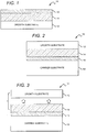
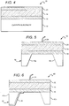
- FIGs. 1 through 5 show one embodiment of a BAW device 10 according to the present invention at different steps in one fabrication method according to the present invention.
- the BAW device 10 is shown as a single device, it is understood that typical fabrication processes occur at the wafer level with the devices being separated using known separation processes following wafer level processing.
- the BAW device 10 is shown herein as a single device to simplify the description herein, but it is understood that the invention herein is not limited to single device fabrication.
- the BAW device 10 comprises a growth substrate 12, that can be made of many different materials.
- the growth substrate 12 can be semi-insulating silicon carbide (SiC) such as, for example, a 4H polytype of silicon carbide.
- SiC silicon carbide
- Other silicon carbide candidate polytypes include the 3C, 6H, and 15R polytypes.
- the term "semi-insulating" is used descriptively rather than in an absolute sense.
- the silicon carbide bulk crystal has a resistivity equal to or higher than about 1x 10 5 ⁇ -cm at room temperature.
- SiC substrates are manufactured by, for example, Cree, Inc., of Durham, N.C., the assignee of the present invention, and methods for producing such materials are described, for example, in US Patent Nos. Re. 34,861 ; 4,946,547 ; 5,200,022 ; and 6,218,680 , the contents of which are incorporated herein by reference in their entirety.
- techniques for epitaxial growth of Group III nitrides have been described in, for example, US Patent Nos. 5,210,051 ; 5,393,993 ; 5,523,589 ; and 5,592,501 , the contents of which are also incorporated herein by reference in their entirety.
- silicon carbide may be used as a substrate material
- embodiments of the present invention may utilize other suitable substrate materials. These materials include sapphire, aluminum nitride, aluminum gallium nitride, gallium nitride, silicon, GaAs, ZnO, InP and the like, or any other material or combination of materials capable of supporting growth of a Group-III nitride material.
- An epitaxial layer 14 is grown on the substrate 12 that will serve as the active region for the device 10.
- the layer 14 can be fabricated using known methods such as growth in metalorganic chemical vapor deposition (MOCVD) reactor using known source gasses and typical temperature ranges.
- MOCVD metalorganic chemical vapor deposition
- the epitaxial layer can be made from many different material systems with the preferred being the Group-III nitride material system, and the layer 14 being single crystal Group-III nitride.
- Group III nitride refers to those semiconducting compounds formed between nitrogen and the elements in Group III of the periodic table, usually aluminum (Al), gallium (Ga), and/or indium (In).
- the term also refers to ternary and quaternary compounds, such as AlGaN and AlInGaN.
- the Group III elements can combine with nitrogen to form binary (e.g., GaN), ternary (e.g., AlGaN and AlInN), and quaternary (e.g., AlInGaN) compounds. These compounds all have empirical formulas in which one mole of nitrogen is combined with a total of one mole of the Group III elements. Accordingly, formulas such as Al x Ga 1-x N, where 0 ⁇ x ⁇ 1, are often used to describe them.
- the epitaxial layer 14 can have different thicknesses depending on the desired frequency of operation, with thinner layers being used for higher frequency operation.
- the epitaxial layer has a thickness in the range of approximately 0.01 to 0.4 microns.
- a preferred thickness is in the range of approximately 0.1 to 0.2 microns.
- the epitaxial layer can also comprise more than one layer of Group-III nitride material with the different layers having different compositions.
- a first metal electrode 16 can be deposited on the epitaxial layer 14 using known methods such as sputtering.
- the first metal electrode 16 can comprise typical semiconductor metallization materials such as nickel, gold, platinum, aluminum (Ni/Au/Pt/Al) or combinations thereof.
- the first metal electrode 16 can also have many different thicknesses with a suitable range being approximately 100 angstroms to a few microns. It is understood that in other embodiments according to the present invention, the first electrode 16 can instead be deposited on the carrier wafer (shown in FIG. 2 and described below).
- the growth substrate 12 and epitaxial layer 14 combination can then be mounted to the carrier wafer, on the first electrode 16.
- the first metal electrode 16 is shown as a metal layer, but it is understood that the first metal electrode can be of various geometries such as interdigitated fingers.
- the substrate 12, epitaxial layer 14 and first electrode 16 combination can be flip-chip mounted to a carrier substrate (wafer) 18.
- a carrier substrate wafer
- Many different mounting methods can be used, with a preferred method being wafer bonding accomplished using solder, epoxy, polyamides and polymers for direct bonding.
- the wafer bonding can also be accomplished using anodic bonding.
- the carrier wafer can comprise many different materials of different thicknesses selected to provide structural support.
- the carrier substrate 18 can be electrically conductive and can also be used to integrate additional electronics. Some of the materials that can be used for the carrier substrate 18 include silicon (Si), germanium (Ge), zinc oxide (ZnO), silicon carbide (SiC) and glass.
- the carrier substrate comprises a material such as Ge that has good thermal conductivity to allow heat to conduct away from the epitaxial layer 14 during operation.
- the growth substrate 12 is removed using removal processes such as grinding, laser ablation, and wet or dry etching. Removal of the substrate 12 leaves a single crystal Group-III nitride layer 14 bonded to the carrier substrate 18, with the first metal electrode 16 sandwiched between the epitaxial layer 14 and the carrier substrate 18.
- the epitaxial layer 14 can also be thinned or further processed, such as by etching or grinding, after removal of the growth substrate 12. This can allow for additional control of the epitaxial layer 14 thickness.
- a second metal electrode 20 can be deposited on the exposed surface of the epitaxial layer 14 with the epitaxial layer 14 sandwiched between the first and second electrodes 16, 20. Similar to the first metal electrode 16, the second metal electrode 20 can be deposited using known semiconductor metallization techniques and can comprise typical semiconductor metallization materials such as nickel, gold, platinum, aluminum (Ni/Au/Pt/Al) or combinations thereof, and can also comprise an IDT. The second metal electrode 20 can also have many different thicknesses, with a suitable range of thicknesses being 100 angstroms to a few microns. For embodiments having an electrically conductive carrier substrate 18 electrical contact can be made to the device 10 at the carrier substrate 18 and second metal electrode 20. In one embodiment the second metal electrode 20 can be contacted by a wire bond while the carrier substrate 18 can be contacted directly to the devices mounted surface, such as a printed circuit board (PCB).
- PCB printed circuit board
- the backside of the device 10, and in particular the carrier substrate 18, can be further processed as desired.
- the carrier substrate 18 can be processed using different etch techniques wet etching, plasma etching or laser micromachining to remove a section of the carrier substrate 18 to the first metal electrode 16, resulting in first and second carrier substrate portions 18a, 18b. This allows for different contacting arrangements to the first and second metal electrodes 16, 20.
- the carrier substrate 18 can be made of an electrically conductive material so that an electrical signal can be applied to the first metal electrode 16, through either of the carrier substrate portions 18a, 18b.
- the first carrier substrate 18a can have a contact 22 at its bottom surface, or in other locations and an electrical signal applied to the contact 22 would be conducted to the first electrode 16.
- the second electrode 20 can be contacted in many different ways, such as by a wire bond 24.
- FIG. 6 shows another embodiment of a BAW device 40 according to the present invention having many of the same or similar features as the BAW device shown in FIG. 5 .
- the same reference numerals are used with the understanding that the description of the features above applies to BAW device 40 herein.
- the BAW device 40 comprises an epitaxial layer 14, first electrode 16 and second electrode 20.
- the BAW device 40 has a carrier substrate 42.
- the carrier substrate 42 and its first and second portions 42a, 42b can be electrically insulating or do not efficiently conduct electricity.
- an electrical signal cannot be applied to first electrode 16 through the carrier substrate portions 42a, 42b.
- the BAW device 40 is provided with a conductive layer 44 that can run from the bottom surface of one or both portions 42a, 42b, and in this case runs from the bottom surface of the first portion 42a.
- the conductive layer 44 continues to the second electrode 20 so that an electrical signal applied to the conductive layer 44 is conducted to the fist electrode 16.
- the conductive layer 44 can also comprise typical semiconductor metallization materials applied using known processes as described above, and can comprise a continuous layer or a plurality of conductive paths.
- the second electrode 20 can be contacted using different arrangements, such as a wire bond 24. It is understood that although this conductive layer in this embodiment is shown as being used with carrier substrates that are electrically insulating or do not efficiently conduct electricity, this arrangement can be used with embodiments having an electrically conductive carrier substrate.
- FIG. 7 shows still another embodiment of a BAW device 60 according to the present invention having an epitaxial layer 14, second electrode 20, and carrier substrate 18.
- a first electrode 61 is also included, but in this embodiment it is divided into separate left and right first electrode portions 62, 64.
- a conductive via 66 is also included through the epitaxial layer 14 providing an electrically conductive path between the electrode portion 64 and the second electrode 20.
- the second electrode 61 can be etched into the separation portions 62, 64 following processing of the carrier substrate 12, and the conductive vias 66 can be formed through the epitaxial layer 14 through etching of a pathway through the epitaxial layer 14 and then filling of the pathway during deposition of the first or second electrodes. It is understood that these features can also be formed using other known processes.
- the BAW device 60 can also comprise first and second contacts 68, 70 each of which is at the bottom of a respective one of the portion of the carrier substrate 18.
- the carrier substrate 18 can efficiently conduct electricity, and an electrical signal applied across the contacts 68, 70 is conducted to the epitaxial layer 14.
- the electrical signal applied to the first contact 68 is conducted through the carrier substrate first portion 18a, to the first electrode left portion 62, and to the epitaxial layer 14.
- the electrical signal applied to the second contact is conducted through the carrier substrate second portion 18b, through the second electrode right portion 64, through the conductive vias 66 and to the first electrode 16.
- This arrangement allows for contacting the BAW device without wire bonding and is particularly applicable to surface mount applications. It is understood that the BAW device 60 can also be used with conductive layer and wire bond arrangements as well.
- FIG. 8 shows another embodiment of a BAW device 100 having an epitaxial layer 102, first electrode 104, second electrode 106, and carrier substrate 108.
- the BAW device 100 further comprises integrated devices 110 to the epitaxial layer that can comprise many different devices including but not limited to light emitting diodes (LEDs), laser diodes, detectors, sensors, field effect transistors (FETs), high electron mobility transistors (HEMTs), etc.
- the devices 110 can be interconnected in many different ways such as by conductive traces, and the devices 110 can be formed in the epitaxial layer during growth of the epitaxial layer, or can be formed on the epitaxial layer following removal of the substrate.
- FIG. 8 shows another embodiment of a BAW device 100 having an epitaxial layer 102, first electrode 104, second electrode 106, and carrier substrate 108.
- the BAW device 100 further comprises integrated devices 110 to the epitaxial layer that can comprise many different devices including but not limited to light emitting diodes (LEDs), laser diodes, detectors,
- FIG. 9 shows another embodiment of a BAW device 120 having an epitaxial layer 122, first electrode 124, second electrode 126, and carrier substrate 128, with similar integrated devices 122 formed integral to the carrier substrate 128.
- the epitaxial layer 102 or carrier substrate can comprise other integral advanced features such as acoustic reflectors.
Landscapes
- Physics & Mathematics (AREA)
- Acoustics & Sound (AREA)
- Engineering & Computer Science (AREA)
- Manufacturing & Machinery (AREA)
- Piezo-Electric Or Mechanical Vibrators, Or Delay Or Filter Circuits (AREA)
Applications Claiming Priority (2)
| Application Number | Priority Date | Filing Date | Title |
|---|---|---|---|
| US11/803,449 US7982363B2 (en) | 2007-05-14 | 2007-05-14 | Bulk acoustic device and method for fabricating |
| EP08251672.5A EP1993205B1 (de) | 2007-05-14 | 2008-05-13 | Volumenwellenresonator und Verfahren zu seiner Herstellung |
Related Parent Applications (1)
| Application Number | Title | Priority Date | Filing Date |
|---|---|---|---|
| EP08251672.5A Division EP1993205B1 (de) | 2007-05-14 | 2008-05-13 | Volumenwellenresonator und Verfahren zu seiner Herstellung |
Publications (3)
| Publication Number | Publication Date |
|---|---|
| EP3188366A2 true EP3188366A2 (de) | 2017-07-05 |
| EP3188366A3 EP3188366A3 (de) | 2017-10-04 |
| EP3188366B1 EP3188366B1 (de) | 2020-08-26 |
Family
ID=39720347
Family Applications (2)
| Application Number | Title | Priority Date | Filing Date |
|---|---|---|---|
| EP16199608.7A Active EP3188366B1 (de) | 2007-05-14 | 2008-05-13 | Baw-vorrichtung und verfahren zur herstellung |
| EP08251672.5A Active EP1993205B1 (de) | 2007-05-14 | 2008-05-13 | Volumenwellenresonator und Verfahren zu seiner Herstellung |
Family Applications After (1)
| Application Number | Title | Priority Date | Filing Date |
|---|---|---|---|
| EP08251672.5A Active EP1993205B1 (de) | 2007-05-14 | 2008-05-13 | Volumenwellenresonator und Verfahren zu seiner Herstellung |
Country Status (3)
| Country | Link |
|---|---|
| US (1) | US7982363B2 (de) |
| EP (2) | EP3188366B1 (de) |
| JP (2) | JP4991626B2 (de) |
Cited By (1)
| Publication number | Priority date | Publication date | Assignee | Title |
|---|---|---|---|---|
| CN109103080A (zh) * | 2018-08-14 | 2018-12-28 | 济南晶正电子科技有限公司 | 一种带电极的反向台面超薄晶片及其制备方法 |
Families Citing this family (65)
| Publication number | Priority date | Publication date | Assignee | Title |
|---|---|---|---|---|
| TW201034186A (en) * | 2009-03-10 | 2010-09-16 | Univ Chang Gung | High electron mobility field-effect transistor device |
| FR2951336B1 (fr) | 2009-10-09 | 2017-02-10 | Commissariat Energie Atomique | Dispositif a ondes acoustiques comprenant un filtre a ondes de surface et un filtre a ondes de volume et procede de fabrication |
| US9537465B1 (en) | 2014-06-06 | 2017-01-03 | Akoustis, Inc. | Acoustic resonator device with single crystal piezo material and capacitor on a bulk substrate |
| US9673384B2 (en) | 2014-06-06 | 2017-06-06 | Akoustis, Inc. | Resonance circuit with a single crystal capacitor dielectric material |
| CN106575957B (zh) * | 2014-06-06 | 2019-12-17 | 阿库斯蒂斯有限公司 | 配置有晶体声谐振器设备的集成电路 |
| US9571061B2 (en) | 2014-06-06 | 2017-02-14 | Akoustis, Inc. | Integrated circuit configured with two or more single crystal acoustic resonator devices |
| US9805966B2 (en) | 2014-07-25 | 2017-10-31 | Akoustis, Inc. | Wafer scale packaging |
| US9912314B2 (en) | 2014-07-25 | 2018-03-06 | Akoustics, Inc. | Single crystal acoustic resonator and bulk acoustic wave filter |
| US9716581B2 (en) | 2014-07-31 | 2017-07-25 | Akoustis, Inc. | Mobile communication device configured with a single crystal piezo resonator structure |
| US9917568B2 (en) | 2014-08-26 | 2018-03-13 | Akoustis, Inc. | Membrane substrate structure for single crystal acoustic resonator device |
| US10700665B2 (en) * | 2015-12-04 | 2020-06-30 | Intel Corporation | Film bulk acoustic resonator (FBAR) devices for high frequency RF filters |
| FR3045678B1 (fr) * | 2015-12-22 | 2017-12-22 | Soitec Silicon On Insulator | Procede de fabrication d'une couche piezoelectrique monocristalline et dispositif microelectronique, photonique ou optique comprenant une telle couche |
| FR3045677B1 (fr) | 2015-12-22 | 2019-07-19 | Soitec | Procede de fabrication d'une couche monocristalline, notamment piezoelectrique |
| JP6699927B2 (ja) * | 2016-03-03 | 2020-05-27 | 株式会社ディスコ | Bawデバイス及びbawデバイスの製造方法 |
| US11677372B2 (en) | 2016-03-11 | 2023-06-13 | Akoustis, Inc. | Piezoelectric acoustic resonator with dielectric protective layer manufactured with piezoelectric thin film transfer process |
| US10523180B2 (en) | 2016-03-11 | 2019-12-31 | Akoustis, Inc. | Method and structure for single crystal acoustic resonator devices using thermal recrystallization |
| US10979026B2 (en) | 2016-03-11 | 2021-04-13 | Akoustis, Inc. | 5.5 GHz Wi-fi 5G coexistence acoustic wave resonator RF filter circuit |
| US11689186B2 (en) | 2016-03-11 | 2023-06-27 | Akoustis, Inc. | 5.5 GHz Wi-Fi 5G coexistence acoustic wave resonator RF filter circuit |
| US11558023B2 (en) | 2016-03-11 | 2023-01-17 | Akoustis, Inc. | Method for fabricating an acoustic resonator device |
| US11316496B2 (en) | 2016-03-11 | 2022-04-26 | Akoustis, Inc. | Method and structure for high performance resonance circuit with single crystal piezoelectric capacitor dielectric material |
| US11736177B2 (en) | 2016-03-11 | 2023-08-22 | Akoustis Inc. | Front end modules for 5.6 GHz and 6.6 GHz Wi-Fi acoustic wave resonator RF filter circuits |
| US10581398B2 (en) | 2016-03-11 | 2020-03-03 | Akoustis, Inc. | Method of manufacture for single crystal acoustic resonator devices using micro-vias |
| US11394451B2 (en) | 2016-03-11 | 2022-07-19 | Akoustis, Inc. | Front end module for 6.1 GHz Wi-Fi acoustic wave resonator RF filter circuit |
| US11476825B2 (en) | 2016-03-11 | 2022-10-18 | Akoustis, Inc. | 5.5 GHz Wi-Fi coexistence acoustic wave resonator RF filter circuit |
| US11184079B2 (en) | 2016-03-11 | 2021-11-23 | Akoustis, Inc. | Front end module for 5.5 GHz Wi-Fi acoustic wave resonator RF filter circuit |
| US10217930B1 (en) | 2016-03-11 | 2019-02-26 | Akoustis, Inc. | Method of manufacture for single crystal acoustic resonator devices using micro-vias |
| US10979022B2 (en) | 2016-03-11 | 2021-04-13 | Akoustis, Inc. | 5.2 GHz Wi-Fi acoustic wave resonator RF filter circuit |
| US11451213B2 (en) | 2016-03-11 | 2022-09-20 | Akoustis, Inc. | 5G n79 Wi-Fi acoustic triplexer circuit |
| US11581866B2 (en) | 2016-03-11 | 2023-02-14 | Akoustis, Inc. | RF acoustic wave resonators integrated with high electron mobility transistors including a shared piezoelectric/buffer layer and methods of forming the same |
| US10615773B2 (en) | 2017-09-11 | 2020-04-07 | Akoustis, Inc. | Wireless communication infrastructure system configured with a single crystal piezo resonator and filter structure |
| US11683021B2 (en) | 2016-03-11 | 2023-06-20 | Akoustis, Inc. | 4.5G 3.55-3.7 GHz band bulk acoustic wave resonator RF filter circuit |
| US20210257993A1 (en) | 2016-03-11 | 2021-08-19 | Akoustis, Inc. | Acoustic wave resonator rf filter circuit device |
| US11832521B2 (en) | 2017-10-16 | 2023-11-28 | Akoustis, Inc. | Methods of forming group III-nitride single crystal piezoelectric thin films using ordered deposition and stress neutral template layers |
| US11411168B2 (en) | 2017-10-16 | 2022-08-09 | Akoustis, Inc. | Methods of forming group III piezoelectric thin films via sputtering |
| US10355659B2 (en) | 2016-03-11 | 2019-07-16 | Akoustis, Inc. | Piezoelectric acoustic resonator manufactured with piezoelectric thin film transfer process |
| US11356071B2 (en) | 2016-03-11 | 2022-06-07 | Akoustis, Inc. | Piezoelectric acoustic resonator with improved TCF manufactured with piezoelectric thin film transfer process |
| US10979025B2 (en) | 2016-03-11 | 2021-04-13 | Akoustis, Inc. | 5G band n79 acoustic wave resonator RF filter circuit |
| US11070184B2 (en) | 2016-03-11 | 2021-07-20 | Akoustis, Inc. | Piezoelectric acoustic resonator manufactured with piezoelectric thin film transfer process |
| US10979024B2 (en) | 2016-03-11 | 2021-04-13 | Akoustis, Inc. | 5.2 GHz Wi-Fi coexistence acoustic wave resonator RF filter circuit |
| US10673513B2 (en) | 2016-03-11 | 2020-06-02 | Akoustis, Inc. | Front end module for 5.2 GHz Wi-Fi acoustic wave resonator RF filter circuit |
| US11418169B2 (en) | 2016-03-11 | 2022-08-16 | Akoustis, Inc. | 5G n41 2.6 GHz band acoustic wave resonator RF filter circuit |
| US10985732B2 (en) | 2016-03-11 | 2021-04-20 | Akoustis, Inc. | 5.6 GHz Wi-Fi acoustic wave resonator RF filter circuit |
| US11177868B2 (en) | 2016-03-11 | 2021-11-16 | Akoustis, Inc. | Front end module for 6.5 GHz Wi-Fi acoustic wave resonator RF filter circuit |
| US10979023B2 (en) | 2016-03-11 | 2021-04-13 | Akoustis, Inc. | 5.9 GHz c-V2X and DSRC acoustic wave resonator RF filter circuit |
| US11424728B2 (en) | 2016-03-11 | 2022-08-23 | Akoustis, Inc. | Piezoelectric acoustic resonator manufactured with piezoelectric thin film transfer process |
| US11063576B2 (en) | 2016-03-11 | 2021-07-13 | Akoustis, Inc. | Front end module for 5.6 GHz Wi-Fi acoustic wave resonator RF filter circuit |
| US11411169B2 (en) | 2017-10-16 | 2022-08-09 | Akoustis, Inc. | Methods of forming group III piezoelectric thin films via removal of portions of first sputtered material |
| US11895920B2 (en) | 2016-08-15 | 2024-02-06 | Akoustis, Inc. | Methods of forming group III piezoelectric thin films via removal of portions of first sputtered material |
| WO2018063299A1 (en) * | 2016-09-30 | 2018-04-05 | Intel Corporation | Rf filters and resonators of crystalline iii-n films |
| US10110188B2 (en) | 2016-11-02 | 2018-10-23 | Akoustis, Inc. | Structure and method of manufacture for acoustic resonator or filter devices using improved fabrication conditions and perimeter structure modifications |
| US10431580B1 (en) | 2017-01-12 | 2019-10-01 | Akoustis, Inc. | Monolithic single chip integrated radio frequency front end module configured with single crystal acoustic filter devices |
| US10411181B2 (en) * | 2017-05-30 | 2019-09-10 | Metis Design Corporation | Electrical via providing electrode pair access on a single side of a device |
| US20210234527A1 (en) * | 2017-09-22 | 2021-07-29 | Anhui Anuki Technologies Co., Ltd. | Manufacturing Method for Piezoelectric Resonator and Piezoelectric Resonator |
| US11856858B2 (en) | 2017-10-16 | 2023-12-26 | Akoustis, Inc. | Methods of forming doped crystalline piezoelectric thin films via MOCVD and related doped crystalline piezoelectric thin films |
| US11557716B2 (en) | 2018-02-20 | 2023-01-17 | Akoustis, Inc. | Method and structure of single crystal electronic devices with enhanced strain interface regions by impurity introduction |
| WO2020046995A1 (en) | 2018-08-27 | 2020-03-05 | Akoustis, Inc. | High power bulk acoustic wave resonator filter devices |
| CN109995340B (zh) * | 2019-03-13 | 2022-03-15 | 电子科技大学 | 一种空腔型体声波谐振器及其制备方法 |
| US11618968B2 (en) | 2020-02-07 | 2023-04-04 | Akoustis, Inc. | Apparatus including horizontal flow reactor with a central injector column having separate conduits for low-vapor pressure metalorganic precursors and other precursors for formation of piezoelectric layers on wafers |
| US12102010B2 (en) | 2020-03-05 | 2024-09-24 | Akoustis, Inc. | Methods of forming films including scandium at low temperatures using chemical vapor deposition to provide piezoelectric resonator devices and/or high electron mobility transistor devices |
| US11496108B2 (en) | 2020-08-17 | 2022-11-08 | Akoustis, Inc. | RF BAW resonator filter architecture for 6.5GHz Wi-Fi 6E coexistence and other ultra-wideband applications |
| CN111933786A (zh) * | 2020-08-17 | 2020-11-13 | 东莞传晟光电有限公司 | 热释电传感器的感应元及其制造方法、热释电传感器 |
| US12255637B2 (en) | 2021-01-18 | 2025-03-18 | Akoustis, Inc. | 5.1-7.1GHz Wi-Fi6E coexistence acoustic wave resonator RF diplexer circuit |
| US11901880B2 (en) | 2021-01-18 | 2024-02-13 | Akoustis, Inc. | 5 and 6 GHz Wi-Fi coexistence acoustic wave resonator RF diplexer circuit |
| CN116246951B (zh) * | 2023-01-18 | 2025-12-30 | 浙江芯科半导体有限公司 | 一种从生长基板上剥离GaN外延层的方法 |
| JP7871965B1 (ja) * | 2025-06-12 | 2026-06-09 | 三菱電機株式会社 | 半導体装置および高周波モジュール |
Family Cites Families (31)
| Publication number | Priority date | Publication date | Assignee | Title |
|---|---|---|---|---|
| US4866005A (en) | 1987-10-26 | 1989-09-12 | North Carolina State University | Sublimation of silicon carbide to produce large, device quality single crystals of silicon carbide |
| US4946547A (en) | 1989-10-13 | 1990-08-07 | Cree Research, Inc. | Method of preparing silicon carbide surfaces for crystal growth |
| US5210051A (en) | 1990-03-27 | 1993-05-11 | Cree Research, Inc. | High efficiency light emitting diodes from bipolar gallium nitride |
| US5200022A (en) | 1990-10-03 | 1993-04-06 | Cree Research, Inc. | Method of improving mechanically prepared substrate surfaces of alpha silicon carbide for deposition of beta silicon carbide thereon and resulting product |
| US5393993A (en) | 1993-12-13 | 1995-02-28 | Cree Research, Inc. | Buffer structure between silicon carbide and gallium nitride and resulting semiconductor devices |
| US5523589A (en) | 1994-09-20 | 1996-06-04 | Cree Research, Inc. | Vertical geometry light emitting diode with group III nitride active layer and extended lifetime |
| US5592501A (en) | 1994-09-20 | 1997-01-07 | Cree Research, Inc. | Low-strain laser structures with group III nitride active layers |
| JPH10308640A (ja) * | 1997-05-07 | 1998-11-17 | Matsushita Electric Ind Co Ltd | 圧電デバイスの製造方法 |
| US6218680B1 (en) | 1999-05-18 | 2001-04-17 | Cree, Inc. | Semi-insulating silicon carbide without vanadium domination |
| TW540173B (en) * | 2002-05-03 | 2003-07-01 | Asia Pacific Microsystems Inc | Bulk acoustic device having integrated fine-tuning and trimming devices |
| US7112860B2 (en) | 2003-03-03 | 2006-09-26 | Cree, Inc. | Integrated nitride-based acoustic wave devices and methods of fabricating integrated nitride-based acoustic wave devices |
| JP2004320127A (ja) * | 2003-04-11 | 2004-11-11 | Tdk Corp | 薄膜圧電共振子の製造方法、薄膜圧電共振子の製造装置、薄膜圧電共振子および電子部品 |
| KR100485702B1 (ko) * | 2003-05-29 | 2005-04-28 | 삼성전자주식회사 | 지지대를 갖는 박막 벌크 음향 공진기 및 그 제조방법 |
| JP4679810B2 (ja) * | 2003-08-27 | 2011-05-11 | 日本碍子株式会社 | エピタキシャル基板、半導体積層構造、エピタキシャル基板の製造方法、およびエピタキシャル基板表面におけるピット発生抑制方法 |
| US6946928B2 (en) * | 2003-10-30 | 2005-09-20 | Agilent Technologies, Inc. | Thin-film acoustically-coupled transformer |
| JP2005176333A (ja) * | 2003-11-18 | 2005-06-30 | Matsushita Electric Ind Co Ltd | 音響共振器装置、フィルタ装置、音響共振器装置の製造方法および通信機器 |
| US7323805B2 (en) | 2004-01-28 | 2008-01-29 | Kabushiki Kaisha Toshiba | Piezoelectric thin film device and method for manufacturing the same |
| JP2005303573A (ja) * | 2004-04-09 | 2005-10-27 | Toshiba Corp | 薄膜圧電共振器及びその製造方法 |
| JP4077805B2 (ja) * | 2004-04-23 | 2008-04-23 | 松下電器産業株式会社 | 共振器の製造方法 |
| JP4280198B2 (ja) * | 2004-04-30 | 2009-06-17 | 株式会社東芝 | 薄膜圧電共振器 |
| JP4712450B2 (ja) * | 2004-06-29 | 2011-06-29 | 日本碍子株式会社 | AlN結晶の表面平坦性改善方法 |
| JP2006024995A (ja) * | 2004-07-06 | 2006-01-26 | Matsushita Electric Ind Co Ltd | 共振器の製造方法 |
| DE102004037818B4 (de) * | 2004-08-04 | 2022-02-17 | Snaptrack, Inc. | Filteranordnung mit zwei Volumenwellenresonatoren |
| JP4078562B2 (ja) * | 2004-08-23 | 2008-04-23 | セイコーエプソン株式会社 | 圧電薄膜共振子の製造方法、圧電薄膜共振子、周波数フィルタ、発振器の製造方法、発振器、電子回路、および電子機器 |
| JP4016983B2 (ja) * | 2004-12-07 | 2007-12-05 | 株式会社村田製作所 | 圧電薄膜共振子およびその製造方法 |
| JP2006191304A (ja) | 2005-01-05 | 2006-07-20 | Matsushita Electric Ind Co Ltd | 圧電共振器及びその製造方法 |
| KR100631217B1 (ko) * | 2005-07-27 | 2006-10-04 | 삼성전자주식회사 | 박막 벌크 음향 공진기 및 표면 음향파 공진기가 집적된인티그레이티드 필터 및 그 제작 방법 |
| JP2007059470A (ja) * | 2005-08-22 | 2007-03-08 | Sony Corp | 半導体装置およびその製造方法 |
| JP4707503B2 (ja) * | 2005-08-25 | 2011-06-22 | パナソニック株式会社 | 薄膜バルク音響共振器 |
| JP2007067624A (ja) * | 2005-08-30 | 2007-03-15 | Seiko Epson Corp | 圧電薄膜振動子 |
| JP2007088819A (ja) * | 2005-09-22 | 2007-04-05 | Seiko Epson Corp | 圧電薄膜振動子 |
-
2007
- 2007-05-14 US US11/803,449 patent/US7982363B2/en active Active
-
2008
- 2008-05-13 EP EP16199608.7A patent/EP3188366B1/de active Active
- 2008-05-13 EP EP08251672.5A patent/EP1993205B1/de active Active
- 2008-05-14 JP JP2008126609A patent/JP4991626B2/ja active Active
-
2012
- 2012-05-02 JP JP2012105274A patent/JP5684193B2/ja active Active
Non-Patent Citations (3)
| Title |
|---|
| DUBOIS, THIN FILM BULK ACOUSTIC WAVE RESONATORS: A TECHNOLOGY OVERVIEW, 2 July 2003 (2003-07-02) |
| PALACIOS ET AL.: "Remote Collection and Measurement of Photogenerated Carriers Swept by Surface Acoustic Waves in GaN", APPLIED PHYSICS LETTERS, vol. 84, no. 16, pages 3162 - 3168 |
| PETRONI ET AL.: "GaN Based Surface Acoustic Wave Filters for Wireless Communications", SUPERLATTICES AND MICROSTRUCTURES, vol. 36, 2004, pages 825 - 831, XP004655584, DOI: doi:10.1016/j.spmi.2004.09.038 |
Cited By (1)
| Publication number | Priority date | Publication date | Assignee | Title |
|---|---|---|---|---|
| CN109103080A (zh) * | 2018-08-14 | 2018-12-28 | 济南晶正电子科技有限公司 | 一种带电极的反向台面超薄晶片及其制备方法 |
Also Published As
| Publication number | Publication date |
|---|---|
| US7982363B2 (en) | 2011-07-19 |
| EP3188366A3 (de) | 2017-10-04 |
| JP4991626B2 (ja) | 2012-08-01 |
| JP5684193B2 (ja) | 2015-03-11 |
| JP2012199934A (ja) | 2012-10-18 |
| US20080284541A1 (en) | 2008-11-20 |
| EP1993205B1 (de) | 2016-12-21 |
| EP1993205A1 (de) | 2008-11-19 |
| JP2008283689A (ja) | 2008-11-20 |
| EP3188366B1 (de) | 2020-08-26 |
Similar Documents
| Publication | Publication Date | Title |
|---|---|---|
| EP1993205B1 (de) | Volumenwellenresonator und Verfahren zu seiner Herstellung | |
| CN205195673U (zh) | 晶圆级封装装置 | |
| US11831295B2 (en) | Multifunctional integrated acoustic devices and systems using epitaxial materials | |
| US9837598B2 (en) | Piezoelectric bulk wave device, and method of manufacturing the piezoelectric bulk wave device | |
| US20190288667A1 (en) | Elastic wave device | |
| KR20020020850A (ko) | 음향 공진기 배치 처리 방법 | |
| TWI735913B (zh) | 電極界定共振器 | |
| US20150287905A1 (en) | Piezoelectric member, acoustic wave apparatus, and piezoelectric member manufacturing method | |
| KR102591286B1 (ko) | 전극 정의 공진기 | |
| JP2006060385A (ja) | 共振器及びそれを用いるフィルタ | |
| CN112204879B (zh) | 电可调表面声波谐振器 | |
| US12068735B2 (en) | Acoustic wave device and manufacturing method thereof | |
| US9530956B2 (en) | Piezoelectric bulk wave device, and method of manufacturing the piezoelectric bulk wave device | |
| CN106575957A (zh) | 配置有晶体声谐振器设备的集成电路 | |
| US6300706B1 (en) | Compound semiconductor monolithic frequency sources and actuators | |
| US7164222B2 (en) | Film bulk acoustic resonator (FBAR) with high thermal conductivity | |
| TWI810698B (zh) | 電極界定未懸掛之聲波共振器 | |
| JP2025075530A (ja) | 弾性波共振器および集積回路 | |
| US11784627B2 (en) | Lamb wave resonator and method of fabricating the same | |
| Neculoiu et al. | Microwave FBAR structures fabricated using micromachined GaN membranes | |
| Ren et al. | Pop-down FBAR structure for thermal stability without sacrificing coupling | |
| WO2021083898A1 (en) | Baw resonator arrangement with resonators having different resonance frequencies and manufacturing method | |
| US12445104B2 (en) | FBAR filter with trap rich layer | |
| WO2009088883A2 (en) | Low-defect-density crystalline structure and method for making same | |
| Muller et al. | GHz FBAR and SAW resonators manufactured on GaN/Si |
Legal Events
| Date | Code | Title | Description |
|---|---|---|---|
| PUAI | Public reference made under article 153(3) epc to a published international application that has entered the european phase |
Free format text: ORIGINAL CODE: 0009012 |
|
| STAA | Information on the status of an ep patent application or granted ep patent |
Free format text: STATUS: THE APPLICATION HAS BEEN PUBLISHED |
|
| AC | Divisional application: reference to earlier application |
Ref document number: 1993205 Country of ref document: EP Kind code of ref document: P |
|
| AK | Designated contracting states |
Kind code of ref document: A2 Designated state(s): DE FR GB |
|
| PUAL | Search report despatched |
Free format text: ORIGINAL CODE: 0009013 |
|
| AK | Designated contracting states |
Kind code of ref document: A3 Designated state(s): DE FR GB |
|
| RIC1 | Information provided on ipc code assigned before grant |
Ipc: H03H 9/17 20060101ALI20170828BHEP Ipc: H03H 3/02 20060101AFI20170828BHEP Ipc: H03H 3/04 20060101ALI20170828BHEP Ipc: H03H 9/05 20060101ALI20170828BHEP |
|
| STAA | Information on the status of an ep patent application or granted ep patent |
Free format text: STATUS: REQUEST FOR EXAMINATION WAS MADE |
|
| 17P | Request for examination filed |
Effective date: 20180404 |
|
| RBV | Designated contracting states (corrected) |
Designated state(s): DE FR GB |
|
| STAA | Information on the status of an ep patent application or granted ep patent |
Free format text: STATUS: EXAMINATION IS IN PROGRESS |
|
| 17Q | First examination report despatched |
Effective date: 20181126 |
|
| GRAP | Despatch of communication of intention to grant a patent |
Free format text: ORIGINAL CODE: EPIDOSNIGR1 |
|
| STAA | Information on the status of an ep patent application or granted ep patent |
Free format text: STATUS: GRANT OF PATENT IS INTENDED |
|
| INTG | Intention to grant announced |
Effective date: 20200313 |
|
| GRAS | Grant fee paid |
Free format text: ORIGINAL CODE: EPIDOSNIGR3 |
|
| GRAA | (expected) grant |
Free format text: ORIGINAL CODE: 0009210 |
|
| STAA | Information on the status of an ep patent application or granted ep patent |
Free format text: STATUS: THE PATENT HAS BEEN GRANTED |
|
| AC | Divisional application: reference to earlier application |
Ref document number: 1993205 Country of ref document: EP Kind code of ref document: P |
|
| AK | Designated contracting states |
Kind code of ref document: B1 Designated state(s): DE FR GB |
|
| REG | Reference to a national code |
Ref country code: GB Ref legal event code: FG4D |
|
| REG | Reference to a national code |
Ref country code: DE Ref legal event code: R096 Ref document number: 602008063193 Country of ref document: DE |
|
| REG | Reference to a national code |
Ref country code: DE Ref legal event code: R097 Ref document number: 602008063193 Country of ref document: DE |
|
| PLBE | No opposition filed within time limit |
Free format text: ORIGINAL CODE: 0009261 |
|
| STAA | Information on the status of an ep patent application or granted ep patent |
Free format text: STATUS: NO OPPOSITION FILED WITHIN TIME LIMIT |
|
| 26N | No opposition filed |
Effective date: 20210527 |
|
| GBPC | Gb: european patent ceased through non-payment of renewal fee |
Effective date: 20210513 |
|
| PG25 | Lapsed in a contracting state [announced via postgrant information from national office to epo] |
Ref country code: GB Free format text: LAPSE BECAUSE OF NON-PAYMENT OF DUE FEES Effective date: 20210513 |
|
| PG25 | Lapsed in a contracting state [announced via postgrant information from national office to epo] |
Ref country code: FR Free format text: LAPSE BECAUSE OF NON-PAYMENT OF DUE FEES Effective date: 20210531 |
|
| REG | Reference to a national code |
Ref country code: DE Ref legal event code: R081 Ref document number: 602008063193 Country of ref document: DE Owner name: WOLFSPEED, INC., DURHAM, US Free format text: FORMER OWNER: CREE, INC., DURHAM, N.C., US Ref country code: DE Ref legal event code: R081 Ref document number: 602008063193 Country of ref document: DE Owner name: MACOM TECHNOLOGY SOLUTIONS HOLDINGS, INC., LOW, US Free format text: FORMER OWNER: CREE, INC., DURHAM, N.C., US |
|
| REG | Reference to a national code |
Ref country code: DE Ref legal event code: R081 Ref document number: 602008063193 Country of ref document: DE Owner name: MACOM TECHNOLOGY SOLUTIONS HOLDINGS, INC., LOW, US Free format text: FORMER OWNER: WOLFSPEED, INC., DURHAM, NC, US |
|
| PGFP | Annual fee paid to national office [announced via postgrant information from national office to epo] |
Ref country code: DE Payment date: 20260522 Year of fee payment: 19 |