EP3186888B1 - Circuits, methods, and systems with optimized operation of double-base bipolar junction transistors - Google Patents
Circuits, methods, and systems with optimized operation of double-base bipolar junction transistors Download PDFInfo
- Publication number
- EP3186888B1 EP3186888B1 EP15857050.7A EP15857050A EP3186888B1 EP 3186888 B1 EP3186888 B1 EP 3186888B1 EP 15857050 A EP15857050 A EP 15857050A EP 3186888 B1 EP3186888 B1 EP 3186888B1
- Authority
- EP
- European Patent Office
- Prior art keywords
- base
- voltage
- collector
- emitter
- region
- Prior art date
- Legal status (The legal status is an assumption and is not a legal conclusion. Google has not performed a legal analysis and makes no representation as to the accuracy of the status listed.)
- Active
Links
Images


Classifications
-
- H—ELECTRICITY
- H02—GENERATION; CONVERSION OR DISTRIBUTION OF ELECTRIC POWER
- H02M—APPARATUS FOR CONVERSION BETWEEN AC AND AC, BETWEEN AC AND DC, OR BETWEEN DC AND DC, AND FOR USE WITH MAINS OR SIMILAR POWER SUPPLY SYSTEMS; CONVERSION OF DC OR AC INPUT POWER INTO SURGE OUTPUT POWER; CONTROL OR REGULATION THEREOF
- H02M1/00—Details of apparatus for conversion
- H02M1/08—Circuits specially adapted for the generation of control voltages for semiconductor devices incorporated in static converters
-
- H—ELECTRICITY
- H03—ELECTRONIC CIRCUITRY
- H03K—PULSE TECHNIQUE
- H03K17/00—Electronic switching or gating, i.e. not by contact-making and –breaking
- H03K17/06—Modifications for ensuring a fully conducting state
-
- H—ELECTRICITY
- H02—GENERATION; CONVERSION OR DISTRIBUTION OF ELECTRIC POWER
- H02M—APPARATUS FOR CONVERSION BETWEEN AC AND AC, BETWEEN AC AND DC, OR BETWEEN DC AND DC, AND FOR USE WITH MAINS OR SIMILAR POWER SUPPLY SYSTEMS; CONVERSION OF DC OR AC INPUT POWER INTO SURGE OUTPUT POWER; CONTROL OR REGULATION THEREOF
- H02M7/00—Conversion of AC power input into DC power output; Conversion of DC power input into AC power output
- H02M7/02—Conversion of AC power input into DC power output without possibility of reversal
- H02M7/04—Conversion of AC power input into DC power output without possibility of reversal by static converters
- H02M7/12—Conversion of AC power input into DC power output without possibility of reversal by static converters using discharge tubes with control electrode or semiconductor devices with control electrode
- H02M7/21—Conversion of AC power input into DC power output without possibility of reversal by static converters using discharge tubes with control electrode or semiconductor devices with control electrode using devices of a triode or transistor type requiring continuous application of a control signal
- H02M7/217—Conversion of AC power input into DC power output without possibility of reversal by static converters using discharge tubes with control electrode or semiconductor devices with control electrode using devices of a triode or transistor type requiring continuous application of a control signal using semiconductor devices only
- H02M7/219—Conversion of AC power input into DC power output without possibility of reversal by static converters using discharge tubes with control electrode or semiconductor devices with control electrode using devices of a triode or transistor type requiring continuous application of a control signal using semiconductor devices only in a bridge configuration
-
- H—ELECTRICITY
- H03—ELECTRONIC CIRCUITRY
- H03K—PULSE TECHNIQUE
- H03K17/00—Electronic switching or gating, i.e. not by contact-making and –breaking
- H03K17/51—Electronic switching or gating, i.e. not by contact-making and –breaking characterised by the components used
- H03K17/56—Electronic switching or gating, i.e. not by contact-making and –breaking characterised by the components used by the use, as active elements, of semiconductor devices
- H03K17/60—Electronic switching or gating, i.e. not by contact-making and –breaking characterised by the components used by the use, as active elements, of semiconductor devices the devices being bipolar transistors
- H03K17/602—Electronic switching or gating, i.e. not by contact-making and –breaking characterised by the components used by the use, as active elements, of semiconductor devices the devices being bipolar transistors in integrated circuits
-
- H—ELECTRICITY
- H03—ELECTRONIC CIRCUITRY
- H03K—PULSE TECHNIQUE
- H03K17/00—Electronic switching or gating, i.e. not by contact-making and –breaking
- H03K17/51—Electronic switching or gating, i.e. not by contact-making and –breaking characterised by the components used
- H03K17/56—Electronic switching or gating, i.e. not by contact-making and –breaking characterised by the components used by the use, as active elements, of semiconductor devices
- H03K17/60—Electronic switching or gating, i.e. not by contact-making and –breaking characterised by the components used by the use, as active elements, of semiconductor devices the devices being bipolar transistors
- H03K17/66—Switching arrangements for passing the current in either direction at will; Switching arrangements for reversing the current at will
-
- H—ELECTRICITY
- H03—ELECTRONIC CIRCUITRY
- H03K—PULSE TECHNIQUE
- H03K17/00—Electronic switching or gating, i.e. not by contact-making and –breaking
- H03K17/51—Electronic switching or gating, i.e. not by contact-making and –breaking characterised by the components used
- H03K17/56—Electronic switching or gating, i.e. not by contact-making and –breaking characterised by the components used by the use, as active elements, of semiconductor devices
- H03K17/687—Electronic switching or gating, i.e. not by contact-making and –breaking characterised by the components used by the use, as active elements, of semiconductor devices the devices being field-effect transistors
-
- H—ELECTRICITY
- H10—SEMICONDUCTOR DEVICES; ELECTRIC SOLID-STATE DEVICES NOT OTHERWISE PROVIDED FOR
- H10D—INORGANIC ELECTRIC SEMICONDUCTOR DEVICES
- H10D18/00—Thyristors
- H10D18/80—Bidirectional devices, e.g. triacs
-
- H—ELECTRICITY
- H10—SEMICONDUCTOR DEVICES; ELECTRIC SOLID-STATE DEVICES NOT OTHERWISE PROVIDED FOR
- H10D—INORGANIC ELECTRIC SEMICONDUCTOR DEVICES
- H10D62/00—Semiconductor bodies, or regions thereof, of devices having potential barriers
- H10D62/10—Shapes, relative sizes or dispositions of the regions of the semiconductor bodies; Shapes of the semiconductor bodies
- H10D62/113—Isolations within a component, i.e. internal isolations
- H10D62/115—Dielectric isolations, e.g. air gaps
-
- H—ELECTRICITY
- H10—SEMICONDUCTOR DEVICES; ELECTRIC SOLID-STATE DEVICES NOT OTHERWISE PROVIDED FOR
- H10D—INORGANIC ELECTRIC SEMICONDUCTOR DEVICES
- H10D62/00—Semiconductor bodies, or regions thereof, of devices having potential barriers
- H10D62/10—Shapes, relative sizes or dispositions of the regions of the semiconductor bodies; Shapes of the semiconductor bodies
- H10D62/13—Semiconductor regions connected to electrodes carrying current to be rectified, amplified or switched, e.g. source or drain regions
- H10D62/133—Emitter regions of BJTs
-
- H—ELECTRICITY
- H10—SEMICONDUCTOR DEVICES; ELECTRIC SOLID-STATE DEVICES NOT OTHERWISE PROVIDED FOR
- H10D—INORGANIC ELECTRIC SEMICONDUCTOR DEVICES
- H10D62/00—Semiconductor bodies, or regions thereof, of devices having potential barriers
- H10D62/10—Shapes, relative sizes or dispositions of the regions of the semiconductor bodies; Shapes of the semiconductor bodies
- H10D62/13—Semiconductor regions connected to electrodes carrying current to be rectified, amplified or switched, e.g. source or drain regions
- H10D62/137—Collector regions of BJTs
-
- H—ELECTRICITY
- H10—SEMICONDUCTOR DEVICES; ELECTRIC SOLID-STATE DEVICES NOT OTHERWISE PROVIDED FOR
- H10D—INORGANIC ELECTRIC SEMICONDUCTOR DEVICES
- H10D62/00—Semiconductor bodies, or regions thereof, of devices having potential barriers
- H10D62/10—Shapes, relative sizes or dispositions of the regions of the semiconductor bodies; Shapes of the semiconductor bodies
- H10D62/17—Semiconductor regions connected to electrodes not carrying current to be rectified, amplified or switched, e.g. channel regions
- H10D62/177—Base regions of bipolar transistors, e.g. BJTs or IGBTs
-
- H—ELECTRICITY
- H10—SEMICONDUCTOR DEVICES; ELECTRIC SOLID-STATE DEVICES NOT OTHERWISE PROVIDED FOR
- H10D—INORGANIC ELECTRIC SEMICONDUCTOR DEVICES
- H10D62/00—Semiconductor bodies, or regions thereof, of devices having potential barriers
- H10D62/10—Shapes, relative sizes or dispositions of the regions of the semiconductor bodies; Shapes of the semiconductor bodies
- H10D62/17—Semiconductor regions connected to electrodes not carrying current to be rectified, amplified or switched, e.g. channel regions
- H10D62/393—Body regions of DMOS transistors or IGBTs
-
- H—ELECTRICITY
- H10—SEMICONDUCTOR DEVICES; ELECTRIC SOLID-STATE DEVICES NOT OTHERWISE PROVIDED FOR
- H10D—INORGANIC ELECTRIC SEMICONDUCTOR DEVICES
- H10D8/00—Diodes
- H10D8/60—Schottky-barrier diodes
-
- H—ELECTRICITY
- H10—SEMICONDUCTOR DEVICES; ELECTRIC SOLID-STATE DEVICES NOT OTHERWISE PROVIDED FOR
- H10D—INORGANIC ELECTRIC SEMICONDUCTOR DEVICES
- H10D84/00—Integrated devices formed in or on semiconductor substrates that comprise only semiconducting layers, e.g. on Si wafers or on GaAs-on-Si wafers
- H10D84/101—Integrated devices comprising main components and built-in components, e.g. IGBT having built-in freewheel diode
- H10D84/121—BJTs having built-in components
-
- H—ELECTRICITY
- H10—SEMICONDUCTOR DEVICES; ELECTRIC SOLID-STATE DEVICES NOT OTHERWISE PROVIDED FOR
- H10D—INORGANIC ELECTRIC SEMICONDUCTOR DEVICES
- H10D84/00—Integrated devices formed in or on semiconductor substrates that comprise only semiconducting layers, e.g. on Si wafers or on GaAs-on-Si wafers
- H10D84/101—Integrated devices comprising main components and built-in components, e.g. IGBT having built-in freewheel diode
- H10D84/131—Thyristors having built-in components
- H10D84/135—Thyristors having built-in components the built-in components being diodes
- H10D84/136—Thyristors having built-in components the built-in components being diodes in anti-parallel configurations, e.g. reverse current thyristor [RCT]
-
- H—ELECTRICITY
- H02—GENERATION; CONVERSION OR DISTRIBUTION OF ELECTRIC POWER
- H02M—APPARATUS FOR CONVERSION BETWEEN AC AND AC, BETWEEN AC AND DC, OR BETWEEN DC AND DC, AND FOR USE WITH MAINS OR SIMILAR POWER SUPPLY SYSTEMS; CONVERSION OF DC OR AC INPUT POWER INTO SURGE OUTPUT POWER; CONTROL OR REGULATION THEREOF
- H02M7/00—Conversion of AC power input into DC power output; Conversion of DC power input into AC power output
- H02M7/02—Conversion of AC power input into DC power output without possibility of reversal
- H02M7/04—Conversion of AC power input into DC power output without possibility of reversal by static converters
- H02M7/12—Conversion of AC power input into DC power output without possibility of reversal by static converters using discharge tubes with control electrode or semiconductor devices with control electrode
- H02M7/21—Conversion of AC power input into DC power output without possibility of reversal by static converters using discharge tubes with control electrode or semiconductor devices with control electrode using devices of a triode or transistor type requiring continuous application of a control signal
- H02M7/217—Conversion of AC power input into DC power output without possibility of reversal by static converters using discharge tubes with control electrode or semiconductor devices with control electrode using devices of a triode or transistor type requiring continuous application of a control signal using semiconductor devices only
- H02M7/219—Conversion of AC power input into DC power output without possibility of reversal by static converters using discharge tubes with control electrode or semiconductor devices with control electrode using devices of a triode or transistor type requiring continuous application of a control signal using semiconductor devices only in a bridge configuration
- H02M7/2195—Conversion of AC power input into DC power output without possibility of reversal by static converters using discharge tubes with control electrode or semiconductor devices with control electrode using devices of a triode or transistor type requiring continuous application of a control signal using semiconductor devices only in a bridge configuration the switches being synchronously commutated at the same frequency of the AC input voltage
-
- H—ELECTRICITY
- H03—ELECTRONIC CIRCUITRY
- H03K—PULSE TECHNIQUE
- H03K2217/00—Indexing scheme related to electronic switching or gating, i.e. not by contact-making or -breaking covered by H03K17/00
- H03K2217/0054—Gating switches, e.g. pass gates
-
- H—ELECTRICITY
- H10—SEMICONDUCTOR DEVICES; ELECTRIC SOLID-STATE DEVICES NOT OTHERWISE PROVIDED FOR
- H10D—INORGANIC ELECTRIC SEMICONDUCTOR DEVICES
- H10D10/00—Bipolar junction transistors [BJT]
- H10D10/01—Manufacture or treatment
- H10D10/051—Manufacture or treatment of vertical BJTs
-
- H—ELECTRICITY
- H10—SEMICONDUCTOR DEVICES; ELECTRIC SOLID-STATE DEVICES NOT OTHERWISE PROVIDED FOR
- H10D—INORGANIC ELECTRIC SEMICONDUCTOR DEVICES
- H10D10/00—Bipolar junction transistors [BJT]
- H10D10/40—Vertical BJTs
-
- H—ELECTRICITY
- H10—SEMICONDUCTOR DEVICES; ELECTRIC SOLID-STATE DEVICES NOT OTHERWISE PROVIDED FOR
- H10D—INORGANIC ELECTRIC SEMICONDUCTOR DEVICES
- H10D10/00—Bipolar junction transistors [BJT]
- H10D10/60—Lateral BJTs
-
- H—ELECTRICITY
- H10—SEMICONDUCTOR DEVICES; ELECTRIC SOLID-STATE DEVICES NOT OTHERWISE PROVIDED FOR
- H10D—INORGANIC ELECTRIC SEMICONDUCTOR DEVICES
- H10D88/00—Three-dimensional [3D] integrated devices
- H10D88/101—Three-dimensional [3D] integrated devices comprising components on opposite major surfaces of semiconductor substrates
Definitions
- the present application relates to power switching methods, and particularly to circuits and methods for operation of bipolar power switching transistors which have two distinct and independent base connections.
- B-TRANs Bidirectional bipolar transistor with two base terminals. Such transistors are referred to as "B-TRANs.”
- the transistor preferably uses the bulk of a semiconductor die as a base region, and has two emitter/collector regions on opposite faces of the die. Two distinct base contact regions are also provided - one on each face of the die. Thus, for example, with a p-type semiconductor die, each face would include an n+ emitter/collector region and a p-type base contact region. Isolation trenches and peripheral field-limiting rings are preferably also included, but in essence this is a four-terminal three-layer device.
- FIG. 6 An example of this published structure is generally illustrated in Figure 6 .
- both faces of a semiconductor die 610 carry emitter/collector regions 622 which form a junction with the bulk substrate 610.
- Base contact regions 632 are also present on both faces.
- This example shows an npn structure, so the emitter/collector regions 622 are n-type, and the base contact regions 632 are p-type.
- a shallow n+ contact doping 624 provides ohmic contact from separate terminals EC1 and EC2 (on the two opposite faces of the semiconductor die, in this example) to regions 622
- a shallow p+ contact doping 634 provides ohmic contact from separate terminals B1 and B2 (on the two opposite faces of the die) to regions 632.
- dielectric-filled trenches 640 provide lateral separation between base contact regions 632 and emitter/collector regions 622. (Note that a p-type diffused region may be added to reduce the series resistance between the emitter-to-base junction and the base contact.) B-TRANs can provide significantly better efficiency than is conventionally available for existing static transfer switches; for example, a 1200V B-TRAN has an expected system efficiency of 99.9%.
- Application US 2014-0375287 also describes some surprising aspects of operation of this kind of device. Notably: 1) when the device is turned on, it is preferably first operated merely as a diode, and base drive is then applied to reduce the on-state voltage drop. 2) Base drive is preferably applied to the base nearest whichever emitter/collector region will be acting as the collector (as determined by the external voltage seen at the device terminals). This is very different from typical bipolar transistor operation, where the base contact is (typically) closely connected to the emitter-base junction. 3) A two-stage turnoff sequence is preferably used.
- the transistor In the first stage of turnoff, the transistor is brought out of full bipolar conduction, but still is connected to operate as a diode; in the final state of turnoff diode conduction is blocked too. 4) In the off state, base-emitter voltage (on each side) is limited by an external low-voltage diode which parallels that base-emitter junction. This prevents either of the base-emitter junctions from getting anywhere close to forward bias, and avoids the degradation of breakdown voltage which can occur otherwise.
- the B-TRAN is a fully symmetric device, there is no difference between the two emitter/collector regions.
- the externally applied voltage will determine which side is (instantaneously) acting as the emitter, and which is acting as the collector.
- the two base contact terminals are accordingly referred as the "e-base” and "c-base", where the c-base terminal is on the side of the device which happens to be the collector side at a given moment.
- Figures 3A-3F (taken from published application 2014-0375287 ) show an example of the operating sequence as disclosed in that application.
- Figure 3A shows a sample equivalent circuit for one exemplary NPN BTRAN.
- Body diodes 312A and 312B can correspond to e.g. the upper and lower P-N junctions, respectively. In, for example, the sample embodiment of Figure 1A , these can correspond to the junctions between emitter/collector regions 104A and base regions 102A.
- Switches 314A and 314B can short respective base terminals 108A and 108B to respective emitter/collector terminals 106A and 106B.
- a BTRAN can have six phases of operation in each direction, as follows.
- steps 1-6 can, when modified appropriately, used to operate the device in the opposite direction.
- steps 1-6 can also be modified to operate a PNP BTRAN (e.g. by inverting all relevant polarities).
- the present invention is a system for power switching as defined in Claim 1 of the appended claims. Also provided is a method for power switching as defined in Claim 5. Details of certain embodiments are set out in the dependent claims.
- the present application teaches, among other innovations, methods and circuits for operating a B-TRAN, and modules and systems incorporating some or all of these innovations.
- the present inventor has discovered, surprisingly, that when a B-TRAN is being operated in full-ON transistor mode (i.e. with low voltage drop and high current flow) the collector-side base contact (i.e. the "c-base”) has a high impedance, up to the point where the current flow on the c-base starts to increase significantly. At that point the transistor is already operating with a very low voltage drop, and increased c-base current will degrade gain without much improvement in voltage drop.
- the preferred base drive circuit operates as a voltage-source drive to the c-base (i.e. to the base contact on whichever side of the device is operating as the collector at a given moment).
- the preferred implementation of the drive circuit is operated by control signals to also provide diode-mode turn-on and pre-turnoff operation.
- two separate subcircuits are used, on each of the bases, for drive in different modes: one subcircuit provides an adjustable voltage for c-base drive in full-ON transistor mode, and the other subcircuit clamps one or both bases to the corresponding emitter/collector regions in diode-on mode or in pre-turnoff mode.
- power for the base drive circuit is provided by a self-synchronizing rectifier circuit.
- the base drive voltage used to drive the c-base region (on the collector side) is varied while the base current at that terminal is monitored, so that no more base current than necessary is applied. This avoids reduced gain, and solves the difficult challenge of optimizing base drive in a B-TRAN.
- B-TRANs novel bidirectional bipolar transistors known as "B-TRANs.”
- the operating cycle of a B-TRAN includes, in succession, a "diode turn-on” (or “diode-ON”) state, a low-V ce or “transistor-ON” state, a “pre-turnoff state, and an "active OFF” state.
- the B-TRAN also has a "passive-OFF” state, which keeps its blocking voltage high when normal operation is not happening.
- the present application describes improvements in the operation of these devices.
- One area of improvement has been in the fully ON state (the "transistor-ON" state).
- An important advantage of the B-TRAN is its low voltage drop V CE when fully on. However, it is desirable to maintain a high value for device gain. It is also desirable to keep the device's switching speed and reverse recovery fast. These improvements have been achieved by a better understanding of the device's behavior in the fully ON state.
- NPN B-TRAN NPN B-TRAN
- the physical base is provided by the bulk of the p-type semiconductor die, and the base contact regions are p-type (with p+ contact doping).
- the two emitter/collector regions are n+, and whichever emitter/collector region sees a more positive external voltage will be the collector side. (The principles of operation are the same for PNP B-TRAN devices, with opposite polarity; in such devices the side which sees the more negative external voltage will be the collector side.)
- the base contact region on the collector side will be referred to as the "c-base,” and the other base contact region (on the emitter side) will be referred to as the “e-base.” These base contact regions are not physically different, but behave very differently when an externally applied voltage is present.
- the fully ON state is reached by applying elevated drive voltage to the c-base.
- This provides a low on-state voltage drop with good gain, without reducing the breakdown voltage.
- Device gain is measured as beta, i.e. the ratio of emitter current to base current, but the behavior of the transistor under c-base drive is very different from that of other power bipolar junction transistors.
- Figure 4 shows a partial device model, with a table of values for c-base bias V CB and corresponding voltage drop V CE across the external terminals.
- the collector/emitter terminal at the top of the figure is assumed to be the collector (i.e. connected to the more positive external voltage), so the base contact which is shown connected to the variable voltage source is the c-base.
- Figure 5 shows how the base current I CB on the c-base varies with c-base bias V CB under operating conditions. It should be noted that current I CB is nearly flat over a wide range of values for V CB .
- the e-base In the transistor-on state, the e-base is essentially at a constant voltage - it varies only about 0.1 V from a low drive to a high drive condition.
- the c-base in contrast, is a nearly constant current drive, even as the voltage is varied from 0 V above the collector to about 0.6V above the collector.
- V CE instead of the c-base current changing with c-base voltage, V CE changes.
- a c-base bias of 0V c-base shorted to collector
- Vce is nominally 0.9 V over a large range of current density.
- Raising the c-base bias to 0.1 V above the collector does not change the gain, but it lowers Vce by nominally 0.1 V.
- Raising c-base bias to 0.6V drops Vce to about 0.2 or 0.3 V.
- the differential impedance, in terms of di/dv, of the c-base itself is high.
- the c-base drive current changes very little with c-base to collector voltage V CB over a wide range of values, until V CB gets close to forward biasing the collector/base junction (over 0.6V at 25C in silicon). That is why a voltage-source-type drive is needed.
- C-base current I CB changes with emitter current, increasing with increased emitter current even when V CB remains constant, but not much with changing V CB (up until a value of V CB where I CB begins to increase undesirably).
- the impedance of the e-base is very low, as it keeps a nearly constant voltage while the c-base current is varied.
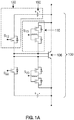
- Figure 1A shows a first example of a complete switch 100, including an NPN B-TRAN transistor 106 as well as diode-mode drive circuitry 110 and transistor-mode drive circuitry 130.
- the half at the top of the page will be assumed to be the collector side, i.e. to be seeing the positive side of the applied voltage.
- Figure 1C shows an example of waveforms during the operation of the circuit of Figure 1A .
- the gate of NMOS S12 is low, and the gate of NMOS S13 is high. This enables the diode-turn-on mode described e.g. in published application US2014-0375287 .
- NMOS transistors S22 and S23 remain off.
- the current I T across the emitter/collector terminals turns on quickly, and voltage V CE across the emitter/collector terminals, which is assumed to have been ramping up under external drive, is brought down to approximately a diode drop (plus some ohmic drop, for a total of about 0.8V in silicon).
- S12 is turned on while S13 is turned off.
- S12 is connected to a variable-voltage source 190, which is derived from the collector terminal as described below.
- This voltage at the c-base drives the transistor into its low-voltage-drop state, where the voltage drop V CE is 0.3V or less. This phase continues for as long as drive current is needed.
- switch S12 is turned off, and switches S13 and S23 are both turned on. This immediately bumps the voltage drop up to a diode drop, but the device current I T remains at a level determined by emitter current density. If this current is not enough to clamp the voltage of the external load, the applied voltage will increase as shown.
- switch S13 is turned off, but switch S23 remains on. This cuts off device current I T , and the voltage on the device goes up to whatever is dictated by the external connections.
- switch S23 was never turned on during this sequence. This switch would be turned on to achieve the transistor-on mode when the external voltage has reversed (so that the emitter/collector terminal node at the top of the page is then the emitter side rather than the collector side).
- FIG 2 shows one sample embodiment of a variable-voltage self-synchronous rectifier, which can be advantageously used in the sample embodiment of Figure 1A .
- a variable-voltage supply 210 (which in the example shown is a simple buck converter) provides an adjustable supply voltage to oscillator 220.
- Oscillator 220 drives a first winding 232 of a transformer 230.
- a first secondary winding 234 provides complementary outputs A and B, which are synchronous with the transitions of oscillator 220, plus the phase shift due to coupling through the transformer 230.
- Another secondary winding 236 provides a higher-current and lower-voltage waveform, corresponding to the output of oscillator 220 (with voltage shifted).
- the output of the two secondary windings is synchronous, so that the control signals A and B can be used to drive the synchronous inverter 240.
- the control signals A and B are preferably scaled to provide appropriate gate voltages for the four transistors of the synchronous inverter, e.g. 5V.
- a 24V DC supply has been efficiently translated into a very-low-voltage DC output whose voltage can be varied.
- the voltage applied to the c-base terminal can be adjusted.
- the bias on the c-base terminal is optimized by adjusting it to the point where base current is no longer constant.
- the c-base contact is high impedance, meaning that the current I CB going into the c-base is nominally constant, when the device is on, until V CB gets close to forward biasing the base-collector junction.
- V CE is well below a diode drop (nominally 0.2V), and I CB starts increasing rapidly with small additional increases in V CB , as shown below.
- V CB is dynamically varied, or "dithered", to find the Optimal Operating Point.
- the Optimal Operating Point should fall where I CB has increased some small but measurable amount above the flat portion of the I CB /V CB curve. This is done by finding a V CB where the slope of the curve is some optimal value.
- V CB 0 V.
- a baseline value for I CB can be found in diode mode, and then a target value is calculated, e.g. by increasing the baseline current value by 10% or 20% or 30%.
- Voltage V CB is then increased in small steps, e.g. in 1% increments, until the measured collector current reaches the target value.
- two limit values can be calculated, and the control voltage V CB ramped back down when the upper limit value for I CB is reached during operation.
- this dithering process can be repeated at short intervals when the transistor is in the ON state for long periods of time.
- Figure 1B shows an example of a more complete base drive circuit. This is slightly different from the drive circuit of Figure 1A in that antiparallel diodes are connected with the body diodes in two of the MOS transistors in the diode-mode drive circuitry 110. Moreover, Figure 1B also shows the JFET plus Schottky branches which form the passive-off protection circuitry 120.
- a B-TRAN is in the "active off-state" when the e-base (base on emitter side) is shorted to the emitter, and the c-base (base on the collector side) is open.
- the collector is the anode (high voltage side)
- the emitter is the cathode (low voltage side).
- the B-TRAN is also off when both bases are open, but due to the high gain of the B-TRAN in this state, the breakdown voltage is low.
- the series combination of a normally-OFF JFET and a Schottky diode attached between each base on its respective emitter/collector, as previously disclosed, will significantly increase the blocking voltage in this "passive off-state".
- the JFETs are turned off during normal operation.
- B-TRAN turn-on is to simultaneously, from the active off-state and blocking forward voltage, open the e-base to emitter short while shorting the c-base to the collector. This immediately introduces charge carriers into the highest field region of the depletion zone around the collector/base junction, so as to achieve very fast, forward biased turn-on for hard switching, very similar to IGBT turn-on.
- the e-base is disconnected from the emitter, and connected to a current or voltage source of sufficient voltage to inject charge carriers into the base region. This method is likely slower, since the charge carriers go into the base just below the depletion zone. Also, it is known that carrier injection into the e-base results in inferior gain relative to carrier injection into the c-base.
- Vce is more than a diode drop.
- turn-on goes to the second stage of increased charge injection into the c-base via a voltage or current source.
- the amount of increased charge injection determines how much V CE is reduced below a diode drop. Injection into the e-base will also reduce V CE , but the gain is much lower than with c-base injection.
- Turn-off can be achieved by any of several methods.
- the most advantageous method is a two-step process.
- the first step the c-base is disconnected from the carrier injection power supply and shorted to the collector, while the previously open e-base is shorted to the emitter. This results in a large current flow between each base and its emitter/collector, which rapidly removes charge carriers from the drift region. This in turn results in a rising Vce as the resistivity of the drift region increases.
- the connection between the c-base and the collector is opened, after which Vce increases rapidly as the depletion region forms around the collector/base junction.
- turn-off can be achieved by simply opening the c-base and shorting the e-base to the emitter, but this will result in higher turn-off losses since the drift region (base) will have a high level of charge carriers at the start of depletion zone formation.
- turn-off can be achieved by simply opening the c-base and leaving the e-base open, but this will result in the highest turn-off losses and also a low breakdown voltage.
- the base drive uses only N-channel MOSFETs to drive the B-TRANs. This makes advantageous use of low MOSFET output voltage (less than 0.7V).
- the input is most preferably variable voltage, which, with current sensing, can be used to determine the optimum base drive voltage.
- Another sample embodiment can support higher voltages, but uses both N-channel and P-channel MOSFETs.
- the present application teaches, among other innovations, methods and circuits for operating a B-TRAN (double-base bidirectional bipolar junction transistor).
- a base drive circuit is described which provides high-impedance drive to the base contact region on whichever side of the device is operating as the collector (at a given moment).
- the B-TRAN unlike other bipolar junction transistors, is controlled by applied voltage rather than applied current.
- the preferred implementation of the drive circuit is operated by control signals to provide diode-mode turn-on and pre-turnoff operation, as well as a hard ON state with a low voltage drop (the "transistor-ON" state).
- an adjustable low voltage for the gate drive circuit is provided by a self-synchronizing rectifier circuit.
- the base drive voltage used to drive the c-base region (on the collector side) is varied while the base current at that terminal is monitored, so that no more base current than necessary is applied. This solves the difficult challenge of optimizing base drive in a B-TRAN.
- a system for power switching comprising: a bidirectional bipolar transistor which has two first-conductivity-type emitter/collector regions separated by a bulk second-conductivity-type base region, and two distinct second-conductivity-type base contact regions which connect to the bulk base region in mutually separate locations; and first and second transistor-mode drive circuits, separately connected to the first and second base contact regions respectively; wherein each drive circuit is configured, as a voltage source, to selectably apply an adjustable voltage between the corresponding base contact region and the emitter/collector region which is nearest to that base contact region; and first and second diode-mode drive circuits, separately connected to the first and second base contact regions respectively; wherein each drive circuit is configured to selectably connect the corresponding base contact region to the emitter/collector region which is nearest to that base contact region.
- a system for power switching comprising: a bidirectional bipolar transistor which has two first-conductivity-type emitter/collector regions separated by a bulk second-conductivity-type base region, and two distinct second-conductivity-type base contact regions which connect to the bulk base region in mutually separate locations; and a pair of transistor-mode drive circuits, separately connected to the first and second base contact regions respectively, wherein each transistor-mode drive circuit is a voltage-mode drive circuit; and a pair of diode-mode drive circuits, separately connected to the first and second base contact regions respectively; wherein each diode-mode drive circuit is configured to selectably connect the corresponding base contact region to the emitter/collector region which is nearest to that base contact region.
- a system for power switching comprising: a bidirectional bipolar transistor which has two first-conductivity-type emitter/collector regions separated by a bulk second-conductivity-type base region, and two distinct second-conductivity-type base contact regions which connect to the bulk base region in mutually separate locations; and a pair of transistor-mode drive circuits, separately connected to the first and second base contact regions respectively; wherein each drive circuit is configured, as a voltage source, to selectably apply an adjustable voltage at a selectable value between the corresponding base contact region and the emitter/collector region which is nearest to that base contact region.
- a method for power switching comprising: driving a bidirectional bipolar transistor which has two first-conductivity-type emitter/collector regions in distinct locations separated by a bulk second-conductivity-type base region, and two distinct second-conductivity-type base contact regions which connect to the bulk base region in mutually separate locations, by in a transistor-ON mode, when minimal voltage drop is desired, using one of a pair of first drive circuits to supply a selected adjustable voltage to the one of the base contact regions which is closest to whichever of the emitter/collector regions is positioned to act as the collector, as defined by externally applied voltage polarity; and in a diode-ON mode, when a diode drop across the device is acceptable, using one of a pair of second drive circuits to clamp one of the base contact regions to the respectively nearest one of the emitter/collector regions; and in a preturnoff mode, using both of the pair of second drive circuits to clamp each of the base contact regions to the respectively nearest
- a method for power switching comprising: driving a bidirectional bipolar transistor which has two first-conductivity-type emitter/collector regions in distinct locations separated by a bulk second-conductivity-type base region, and two distinct second-conductivity-type base contact regions which connect to the bulk base region in mutually separate locations, by in a transistor-ON mode, when minimal voltage drop is desired, using one of a pair of first drive circuits to supply a selected adjustable voltage to the one of the base contact regions which is closest to whichever of the emitter/collector regions is positioned to act as the collector, as defined by externally applied voltage polarity; and in a diode-ON mode, when a diode drop across the device is acceptable, using one of a pair of second drive circuits to clamp one of the base contact regions to the respectively nearest one of the emitter/collector regions.
- a method for power switching comprising: driving a bidirectional bipolar transistor which has two first-conductivity-type emitter/collector regions in distinct locations separated by a bulk second-conductivity-type base region, and two distinct second-conductivity-type base contact regions which connect to the bulk base region in mutually separate locations, by in a transistor-ON mode, when minimal voltage drop is desired, using one of a pair of first drive circuits to supply a selected adjustable voltage to the one of the base contact regions which is closest to whichever of the emitter/collector regions is positioned to act as the collector, as defined by externally applied voltage polarity.
- a method of providing a variable-voltage low-voltage output comprising the actions of: a) providing an adjustable voltage to supply an oscillator; b) using the oscillator to apply an AC waveform to a primary winding of a transformer; c) at one secondary winding of the transformer, generating complementary control signals; and d) using the complementary control signals to operate a synchronous rectifier which is connected to another secondary winding of the same transformer, to thereby provide a low-voltage output.
- a variable-voltage low-voltage power circuit comprising: an adjustable voltage supply circuit, connected to provide an adjustable voltage; an oscillator circuit, connected to receive the adjustable voltage as a supply voltage, and connected to drive a primary winding of a transformer with an AC waveform; a first secondary winding of the transformer, connected to output complementary control signals; and a second secondary winding of the transformer, having fewer turns than the first secondary winding; and a synchronous rectifier, including at least four transistors which are gated by the complementary control signals and are connected in a bridge configuration, which is connected to rectify the output of the secondary winding; wherein the output of the second secondary winding, after rectification by the synchronous rectifier, provides a substantially DC output which is smaller than a diode drop.
- a method of operating a bidirectional bipolar transistor which has first and second first-conductivity-type emitter/collector regions in distinct locations separated by a bulk second-conductivity-type base region, and also has two distinct second-conductivity-type base contact regions which connect to the bulk base region in mutually separate locations, in respective proximity to first and second emitter/collector regions but not to each other, comprising the actions of: a) when low on-state resistance is desired, applying a base drive voltage to whichever of the base contact regions is then on the collector side of the device; and b) varying the base drive voltage while monitoring base current, to thereby find a target base drive voltage where base current begins to increase with base drive voltage; and operating the transistor at approximately the target base drive voltage.
- a system for power switching comprising: a bidirectional bipolar transistor which has two first-conductivity-type emitter/collector regions separated by a bulk second-conductivity-type base region, and two distinct second-conductivity-type base contact regions which connect to the bulk base region in mutually separate locations; and a pair of transistor-mode drive circuits, separately connected to the first and second base contact regions respectively; wherein, during the transistor-ON state where low voltage drop is desired, one of the drive circuits, as determined by external voltage polarity, is configured to apply an adjustable voltage to a selected one of base contact regions, and dither the adjustable voltage, to thereby find an operating point voltage where the current at the selected base contact begins to increase with applied voltage, and then keep the adjustable voltage at approximately the operating point voltage.
- the main embodiments described above use NPN B-TRAN transistors.
- PNP B-TRAN transistors with appropriate inversion of voltages.
- teachings here can be applied to B-TRAN devices of various sizes, depending on what blocking voltage and current capacity are required.
- a single control module can optionally be connected to apply the appropriate control signals to each of the B-TRANs' drive circuits.
- a single B-TRAN drive circuit can optionally be used to drive multiple B-TRANs in parallel. This is not practical with other bipolar junction transistors.
Landscapes
- Engineering & Computer Science (AREA)
- Power Engineering (AREA)
- Microelectronics & Electronic Packaging (AREA)
- Power Conversion In General (AREA)
- Bipolar Integrated Circuits (AREA)
- Bipolar Transistors (AREA)
- Electronic Switches (AREA)
Applications Claiming Priority (8)
| Application Number | Priority Date | Filing Date | Title |
|---|---|---|---|
| US201462076320P | 2014-11-06 | 2014-11-06 | |
| US201562100301P | 2015-01-06 | 2015-01-06 | |
| US201562130470P | 2015-03-09 | 2015-03-09 | |
| US201562162907P | 2015-05-18 | 2015-05-18 | |
| US201562182878P | 2015-06-22 | 2015-06-22 | |
| US201562185543P | 2015-06-26 | 2015-06-26 | |
| US201562194167P | 2015-07-17 | 2015-07-17 | |
| PCT/US2015/059623 WO2016073957A1 (en) | 2014-11-06 | 2015-11-06 | Circuits, methods, and systems with optimized operation of double-base bipolar junction transistors |
Publications (3)
| Publication Number | Publication Date |
|---|---|
| EP3186888A1 EP3186888A1 (en) | 2017-07-05 |
| EP3186888A4 EP3186888A4 (en) | 2018-01-17 |
| EP3186888B1 true EP3186888B1 (en) | 2021-05-05 |
Family
ID=55909934
Family Applications (1)
| Application Number | Title | Priority Date | Filing Date |
|---|---|---|---|
| EP15857050.7A Active EP3186888B1 (en) | 2014-11-06 | 2015-11-06 | Circuits, methods, and systems with optimized operation of double-base bipolar junction transistors |
Country Status (7)
| Country | Link |
|---|---|
| US (4) | US20160204714A1 (https=) |
| EP (1) | EP3186888B1 (https=) |
| JP (1) | JP6659685B2 (https=) |
| KR (1) | KR102450784B1 (https=) |
| CN (1) | CN107371382B (https=) |
| GB (1) | GB2536586B (https=) |
| WO (1) | WO2016073957A1 (https=) |
Cited By (1)
| Publication number | Priority date | Publication date | Assignee | Title |
|---|---|---|---|---|
| WO2024123521A1 (en) * | 2022-12-08 | 2024-06-13 | Ideal Power Inc. | Bidirectional bipolar junction transistor devices from bonded wide and thick wafers |
Families Citing this family (18)
| Publication number | Priority date | Publication date | Assignee | Title |
|---|---|---|---|---|
| US9729144B2 (en) * | 2013-07-31 | 2017-08-08 | Schneider Electric Solar Inverters Usa, Inc. | Isolated uni-polar transistor gate drive |
| US11637016B2 (en) | 2013-12-11 | 2023-04-25 | Ideal Power Inc. | Systems and methods for bidirectional device fabrication |
| US11069797B2 (en) | 2016-05-25 | 2021-07-20 | Ideal Power Inc. | Ruggedized symmetrically bidirectional bipolar power transistor |
| US11135936B2 (en) | 2019-03-06 | 2021-10-05 | Fermata, LLC | Methods for using temperature data to protect electric vehicle battery health during use of bidirectional charger |
| US11335674B2 (en) | 2019-06-27 | 2022-05-17 | Globalfoundries U.S. Inc. | Diode triggered silicon controlled rectifier (SCR) with hybrid diodes |
| US11958372B2 (en) | 2019-11-26 | 2024-04-16 | Fermata Energy Llc | Device for bi-directional power conversion and charging for use with electric vehicles |
| US11430881B2 (en) * | 2020-03-05 | 2022-08-30 | Globalfoundries U.S. Inc. | Diode triggered compact silicon controlled rectifier |
| US11411557B2 (en) | 2020-05-18 | 2022-08-09 | Ideal Power Inc. | Method and system of operating a bi-directional double-base bipolar junction transistor (B-TRAN) |
| US11496129B2 (en) | 2020-06-08 | 2022-11-08 | Ideal Power Inc. | Method and system of current sharing among bidirectional double-base bipolar junction transistors |
| US11777018B2 (en) | 2020-11-19 | 2023-10-03 | Ideal Power Inc. | Layout to reduce current crowding at endpoints |
| JP7605320B2 (ja) * | 2020-12-10 | 2024-12-24 | アイディール パワー インコーポレイテッド | 双方向ダブルベースバイポーラ接合トランジスタ(b-tran)を動作させる方法及びシステム |
| WO2023018769A1 (en) | 2021-08-10 | 2023-02-16 | Ideal Power Inc. | System and method for bi-directional trench power switches |
| CN119156703A (zh) | 2022-05-25 | 2024-12-17 | 理想能量有限公司 | 用于双面双向结型晶体管的双面冷却封装 |
| US12507486B2 (en) | 2022-09-15 | 2025-12-23 | Globalfoundries U.S. Inc. | Vertically integrated SCR structure with SOI-based raised trigger element |
| JPWO2025022733A1 (https=) * | 2023-07-25 | 2025-01-30 | ||
| US12506475B2 (en) | 2023-08-30 | 2025-12-23 | Ideal Power Inc. | Hybrid switch circuit with bidirectional double-base bipolar junction transistors |
| US12388442B2 (en) | 2023-12-06 | 2025-08-12 | Ideal Power Inc. | Unidirectional hybrid switch circuit |
| US12506476B2 (en) | 2024-02-21 | 2025-12-23 | Ideal Power Inc. | Methods and systems of operating a double-sided double-base bipolar junction transistor |
Family Cites Families (64)
| Publication number | Priority date | Publication date | Assignee | Title |
|---|---|---|---|---|
| US3476993A (en) | 1959-09-08 | 1969-11-04 | Gen Electric | Five layer and junction bridging terminal switching device |
| DE2231777A1 (de) | 1971-08-27 | 1973-03-08 | Halbleiterwerk Frankfurt Oder | Symmetrisch schaltendes mehrschichtenbauelement und verfahren zu seiner herstellung |
| US3996601A (en) | 1974-07-15 | 1976-12-07 | Hutson Jerald L | Shorting structure for multilayer semiconductor switching devices |
| CH609714A5 (en) | 1974-07-15 | 1979-03-15 | Agfa Gevaert Ag | Process for the production of a hydrophilic surface on silicone rubber mouldings |
| US4131902A (en) | 1977-09-30 | 1978-12-26 | Westinghouse Electric Corp. | Novel bipolar transistor with a dual-dielectric tunnel emitter |
| US4816892A (en) | 1982-02-03 | 1989-03-28 | General Electric Company | Semiconductor device having turn-on and turn-off capabilities |
| JPS58218168A (ja) | 1982-06-14 | 1983-12-19 | Toshiba Corp | 双方向トランジスタ |
| CA1200322A (en) | 1982-12-13 | 1986-02-04 | General Electric Company | Bidirectional insulated-gate rectifier structures and method of operation |
| JPH0821713B2 (ja) | 1987-02-26 | 1996-03-04 | 株式会社東芝 | 導電変調型mosfet |
| JP2703240B2 (ja) | 1987-12-03 | 1998-01-26 | 株式会社東芝 | 導電変調型mosfet |
| ATE93654T1 (de) | 1988-04-22 | 1993-09-15 | Asea Brown Boveri | Abschaltbares leistungshalbleiterbauelement. |
| FR2635930B1 (fr) * | 1988-08-31 | 1990-11-23 | Sgs Thomson Microelectronics | Commutateur bidirectionnel monolithique a transistors mos de puissance |
| EP0394859A1 (de) * | 1989-04-28 | 1990-10-31 | Asea Brown Boveri Ag | Bidirektionals, abschaltbares Halbeiterbauelement |
| CH678245A5 (https=) | 1989-06-07 | 1991-08-15 | Asea Brown Boveri | |
| JPH03147378A (ja) | 1989-11-02 | 1991-06-24 | Nec Corp | ソリッド・ステート・リレー |
| EP0438700A1 (de) | 1990-01-25 | 1991-07-31 | Asea Brown Boveri Ag | Abschaltbares, MOS-gesteuertes Leistungshalbleiter-Bauelement sowie Verfahren zu dessen Herstellung |
| JP3352840B2 (ja) * | 1994-03-14 | 2002-12-03 | 株式会社東芝 | 逆並列接続型双方向性半導体スイッチ |
| US5852559A (en) | 1996-09-24 | 1998-12-22 | Allen Bradley Company, Llc | Power application circuits utilizing bidirectional insulated gate bipolar transistor |
| US5793064A (en) | 1996-09-24 | 1998-08-11 | Allen Bradley Company, Llc | Bidirectional lateral insulated gate bipolar transistor |
| US5910664A (en) | 1996-11-05 | 1999-06-08 | International Rectifier Corporation | Emitter-switched transistor structures |
| SE9901410D0 (sv) | 1999-04-21 | 1999-04-21 | Abb Research Ltd | Abipolar transistor |
| JP2001069754A (ja) * | 1999-08-27 | 2001-03-16 | Fujitsu Ltd | 同期整流回路 |
| US6961253B1 (en) * | 1999-10-08 | 2005-11-01 | Lambda Electronics | Drive circuits for synchronous rectifiers |
| JP4635304B2 (ja) | 2000-07-12 | 2011-02-23 | 富士電機システムズ株式会社 | 双方向超接合半導体素子およびその製造方法 |
| EP1353385B1 (en) | 2001-01-19 | 2014-09-24 | Mitsubishi Denki Kabushiki Kaisha | Semiconductor device |
| US6674658B2 (en) * | 2001-02-09 | 2004-01-06 | Netpower Technologies, Inc. | Power converter including circuits for improved operational control of synchronous rectifiers therein |
| JP2003164152A (ja) * | 2001-11-26 | 2003-06-06 | Tdk Corp | スイッチング電源装置 |
| GB2380604B (en) | 2001-06-01 | 2005-02-09 | Fuji Electric Co Ltd | Semiconductor switch |
| FR2830127B1 (fr) | 2001-09-21 | 2004-12-24 | St Microelectronics Sa | Commutateur monolithique bidirectionnel vertical a commande en tension |
| US6856520B2 (en) | 2002-05-20 | 2005-02-15 | The United States Of America As Represented By The Secretary Of The Navy | Double sided IGBT phase leg architecture and clocking method for reduced turn on loss |
| CA2427039C (en) * | 2003-04-29 | 2013-08-13 | Kinectrics Inc. | High speed bi-directional solid state switch |
| US7279731B1 (en) * | 2006-05-15 | 2007-10-09 | Udt Sensors, Inc. | Edge illuminated photodiodes |
| JP2004342718A (ja) | 2003-05-14 | 2004-12-02 | Toshiba Corp | 半導体装置及びコンバータ |
| US7064069B2 (en) | 2003-10-21 | 2006-06-20 | Micron Technology, Inc. | Substrate thinning including planarization |
| DE102004005384B4 (de) | 2004-02-03 | 2006-10-26 | De Doncker, Rik W., Prof. Dr. ir. | Bidirektionales, MOS-gesteuertes Halbleiterbauelement, Verfahren zu seinem Betreiben, Verfahren zu seiner Herstellung und seine Verwendung |
| JP4791704B2 (ja) | 2004-04-28 | 2011-10-12 | 三菱電機株式会社 | 逆導通型半導体素子とその製造方法 |
| US7129144B2 (en) * | 2004-04-30 | 2006-10-31 | Lite-On Semiconductor Corp. | Overvoltage protection device and manufacturing process for the same |
| GB0417749D0 (en) | 2004-08-10 | 2004-09-08 | Eco Semiconductors Ltd | Improved bipolar MOSFET devices and methods for their use |
| JP5011681B2 (ja) | 2004-12-02 | 2012-08-29 | 日産自動車株式会社 | 半導体装置 |
| KR100677816B1 (ko) | 2005-03-28 | 2007-02-02 | 산요덴키가부시키가이샤 | 능동 소자 및 스위치 회로 장치 |
| US20060261346A1 (en) | 2005-05-18 | 2006-11-23 | Sei-Hyung Ryu | High voltage silicon carbide devices having bi-directional blocking capabilities and methods of fabricating the same |
| DE102005047101B3 (de) | 2005-09-30 | 2007-01-04 | Infineon Technologies Austria Ag | Halbleiterschalteranordnung und Ansteuerverfahren |
| JP4695961B2 (ja) * | 2005-10-20 | 2011-06-08 | パナソニック株式会社 | 高耐圧半導体スイッチング素子及びそれを用いたスイッチング電源装置 |
| US7354809B2 (en) | 2006-02-13 | 2008-04-08 | Wisconsin Alumi Research Foundation | Method for double-sided processing of thin film transistors |
| US8796750B2 (en) * | 2006-05-15 | 2014-08-05 | Osi Optoelectronics, Inc. | Edge illuminated photodiodes |
| JP4471967B2 (ja) | 2006-12-28 | 2010-06-02 | 株式会社ルネサステクノロジ | 双方向スイッチモジュール |
| JP5251102B2 (ja) | 2007-12-10 | 2013-07-31 | 株式会社デンソー | 半導体装置 |
| JP4912353B2 (ja) | 2008-05-16 | 2012-04-11 | 三菱電機株式会社 | 電力用半導体装置およびその製造方法 |
| JP5245157B2 (ja) | 2008-06-03 | 2013-07-24 | 独立行政法人産業技術総合研究所 | 半導体双方向スイッチング装置 |
| US8163624B2 (en) | 2008-07-30 | 2012-04-24 | Bowman Ronald R | Discrete semiconductor device and method of forming sealed trench junction termination |
| JP2010088259A (ja) * | 2008-10-02 | 2010-04-15 | Shindengen Electric Mfg Co Ltd | スイッチング電源装置およびスイッチング電源装置の制御方法 |
| CN102714465A (zh) * | 2009-06-29 | 2012-10-03 | 理想能量转换器有限公司 | 带有旁路能量转移电抗的消弧开关的功率转移器件、方法和系统 |
| KR101031217B1 (ko) * | 2009-10-21 | 2011-04-27 | 주식회사 오리엔트전자 | 고정 시비율로 동작하는 llc 공진 컨버터를 사용한 2단 방식 절연형 양방향 dc/dc 전력변환기 |
| FR2953995B1 (fr) | 2009-11-24 | 2012-02-10 | St Microelectronics Tours Sas | Interrupteur de puissance bidirectionnel commandable a la fermeture et a l'ouverture |
| US8576583B2 (en) | 2010-09-17 | 2013-11-05 | Fairchild Semiconductor Corporation | Sampled charge control for resonant converter |
| US8735289B2 (en) * | 2010-11-29 | 2014-05-27 | Infineon Technologies Ag | Method of contacting a doping region in a semiconductor substrate |
| JP5754543B2 (ja) | 2012-03-16 | 2015-07-29 | 富士電機株式会社 | 半導体装置 |
| JP2015529442A (ja) * | 2012-08-17 | 2015-10-05 | アドバンスド チャージング テクノロジーズ, エルエルシーAdvanced Charging Technologies,Llc | 電力デバイス |
| US8963253B2 (en) * | 2012-10-23 | 2015-02-24 | Macronix International Co., Ltd. | Bi-directional bipolar junction transistor for high voltage electrostatic discharge protection |
| JP5680050B2 (ja) * | 2012-12-19 | 2015-03-04 | オムロンオートモーティブエレクトロニクス株式会社 | 充電装置 |
| GB2524699C (en) * | 2013-02-07 | 2018-11-14 | Wood John | A bipolar junction transistor structure |
| US9082648B2 (en) | 2013-02-27 | 2015-07-14 | Pakal Technologies Llc | Vertical insulated-gate turn-off device having a planar gate |
| EP3116028B1 (en) * | 2013-06-24 | 2021-03-24 | Ideal Power Inc. | Systems, circuits, devices, and methods with bidirectional bipolar transistors |
| US9490704B2 (en) * | 2014-02-12 | 2016-11-08 | Delta Electronics, Inc. | System and methods for controlling secondary side switches in resonant power converters |
-
2015
- 2015-11-06 EP EP15857050.7A patent/EP3186888B1/en active Active
- 2015-11-06 US US14/935,336 patent/US20160204714A1/en not_active Abandoned
- 2015-11-06 KR KR1020177011835A patent/KR102450784B1/ko active Active
- 2015-11-06 GB GB1610455.6A patent/GB2536586B/en active Active
- 2015-11-06 WO PCT/US2015/059623 patent/WO2016073957A1/en not_active Ceased
- 2015-11-06 US US14/935,344 patent/US9444449B2/en active Active
- 2015-11-06 JP JP2017524461A patent/JP6659685B2/ja active Active
- 2015-11-06 CN CN201580059244.XA patent/CN107371382B/zh active Active
- 2015-11-06 US US14/935,349 patent/US9660551B2/en active Active
-
2016
- 2016-08-10 US US15/233,306 patent/US9742395B2/en active Active
Cited By (2)
| Publication number | Priority date | Publication date | Assignee | Title |
|---|---|---|---|---|
| WO2024123521A1 (en) * | 2022-12-08 | 2024-06-13 | Ideal Power Inc. | Bidirectional bipolar junction transistor devices from bonded wide and thick wafers |
| GB2638100A (en) * | 2022-12-08 | 2025-08-13 | Ideal Power Inc | Bidirectional bipolar junction transistor devices from bonded wide and thick wafers |
Also Published As
| Publication number | Publication date |
|---|---|
| US20160173083A1 (en) | 2016-06-16 |
| JP6659685B2 (ja) | 2020-03-04 |
| US9660551B2 (en) | 2017-05-23 |
| US20160204779A1 (en) | 2016-07-14 |
| EP3186888A4 (en) | 2018-01-17 |
| WO2016073957A1 (en) | 2016-05-12 |
| US20160204714A1 (en) | 2016-07-14 |
| KR20170078658A (ko) | 2017-07-07 |
| KR102450784B1 (ko) | 2022-10-05 |
| JP2018502542A (ja) | 2018-01-25 |
| GB2536586A (en) | 2016-09-21 |
| EP3186888A1 (en) | 2017-07-05 |
| CN107371382B (zh) | 2020-03-10 |
| GB2536586B (en) | 2018-02-28 |
| GB201610455D0 (en) | 2016-07-27 |
| CN107371382A (zh) | 2017-11-21 |
| US20170126225A1 (en) | 2017-05-04 |
| US9742395B2 (en) | 2017-08-22 |
| US9444449B2 (en) | 2016-09-13 |
Similar Documents
| Publication | Publication Date | Title |
|---|---|---|
| EP3186888B1 (en) | Circuits, methods, and systems with optimized operation of double-base bipolar junction transistors | |
| US10211283B2 (en) | Operation of double-base bipolar transistors with additional timing phases at switching transitions | |
| US10497699B2 (en) | Double-base-connected bipolar transistors with passive components preventing accidental turn-on | |
| US9742385B2 (en) | Bidirectional semiconductor switch with passive turnoff | |
| US4870555A (en) | High-efficiency DC-to-DC power supply with synchronous rectification | |
| EP2427912B1 (en) | Wide bandgap bipolar turn-off thyristor having non-negative temperature coefficient and related control circuits | |
| EP2816729A1 (en) | Depletion mode group III-V transistor with high voltage group IV enable switch | |
| US9799731B2 (en) | Multi-level inverters using sequenced drive of double-base bidirectional bipolar transistors | |
| US10547250B2 (en) | Rectifier device | |
| KR102178107B1 (ko) | 프리휠링 SiC 다이오드를 갖는 RC-IGBT | |
| WO2016112395A1 (en) | Thin-substrate double-base high-voltage bipolar transistors | |
| EP3350914B1 (en) | Operation of double-base bipolar transistors with additional timing phases at switching transitions | |
| US11271547B2 (en) | Gate drive circuit, drive device, semiconductor device, and gate drive method | |
| GB2575810A (en) | Power semiconductor device |
Legal Events
| Date | Code | Title | Description |
|---|---|---|---|
| STAA | Information on the status of an ep patent application or granted ep patent |
Free format text: STATUS: THE INTERNATIONAL PUBLICATION HAS BEEN MADE |
|
| PUAI | Public reference made under article 153(3) epc to a published international application that has entered the european phase |
Free format text: ORIGINAL CODE: 0009012 |
|
| STAA | Information on the status of an ep patent application or granted ep patent |
Free format text: STATUS: REQUEST FOR EXAMINATION WAS MADE |
|
| 17P | Request for examination filed |
Effective date: 20170331 |
|
| AK | Designated contracting states |
Kind code of ref document: A1 Designated state(s): AL AT BE BG CH CY CZ DE DK EE ES FI FR GB GR HR HU IE IS IT LI LT LU LV MC MK MT NL NO PL PT RO RS SE SI SK SM TR |
|
| AX | Request for extension of the european patent |
Extension state: BA ME |
|
| A4 | Supplementary search report drawn up and despatched |
Effective date: 20171214 |
|
| RIC1 | Information provided on ipc code assigned before grant |
Ipc: H02M 3/158 20060101ALI20171208BHEP Ipc: H03K 17/66 20060101AFI20171208BHEP Ipc: H03K 17/687 20060101ALI20171208BHEP |
|
| DAV | Request for validation of the european patent (deleted) | ||
| DAX | Request for extension of the european patent (deleted) | ||
| STAA | Information on the status of an ep patent application or granted ep patent |
Free format text: STATUS: EXAMINATION IS IN PROGRESS |
|
| 17Q | First examination report despatched |
Effective date: 20191111 |
|
| GRAP | Despatch of communication of intention to grant a patent |
Free format text: ORIGINAL CODE: EPIDOSNIGR1 |
|
| STAA | Information on the status of an ep patent application or granted ep patent |
Free format text: STATUS: GRANT OF PATENT IS INTENDED |
|
| INTG | Intention to grant announced |
Effective date: 20210122 |
|
| GRAS | Grant fee paid |
Free format text: ORIGINAL CODE: EPIDOSNIGR3 |
|
| GRAA | (expected) grant |
Free format text: ORIGINAL CODE: 0009210 |
|
| STAA | Information on the status of an ep patent application or granted ep patent |
Free format text: STATUS: THE PATENT HAS BEEN GRANTED |
|
| AK | Designated contracting states |
Kind code of ref document: B1 Designated state(s): AL AT BE BG CH CY CZ DE DK EE ES FI FR GR HR HU IE IS IT LI LT LU LV MC MK MT NL NO PL PT RO RS SE SI SK SM TR |
|
| RBV | Designated contracting states (corrected) |
Designated state(s): AL AT BE BG CH CY CZ DE DK EE ES FI FR GR HR HU IE IS IT LI LT LU LV MC MK MT NL NO PL PT RO RS SE SI SK SM TR |
|
| REG | Reference to a national code |
Ref country code: CH Ref legal event code: EP |
|
| REG | Reference to a national code |
Ref country code: AT Ref legal event code: REF Ref document number: 1391109 Country of ref document: AT Kind code of ref document: T Effective date: 20210515 |
|
| REG | Reference to a national code |
Ref country code: DE Ref legal event code: R096 Ref document number: 602015069108 Country of ref document: DE |
|
| REG | Reference to a national code |
Ref country code: IE Ref legal event code: FG4D |
|
| REG | Reference to a national code |
Ref country code: NL Ref legal event code: FP |
|
| REG | Reference to a national code |
Ref country code: LT Ref legal event code: MG9D |
|
| REG | Reference to a national code |
Ref country code: AT Ref legal event code: MK05 Ref document number: 1391109 Country of ref document: AT Kind code of ref document: T Effective date: 20210505 |
|
| PG25 | Lapsed in a contracting state [announced via postgrant information from national office to epo] |
Ref country code: LT Free format text: LAPSE BECAUSE OF FAILURE TO SUBMIT A TRANSLATION OF THE DESCRIPTION OR TO PAY THE FEE WITHIN THE PRESCRIBED TIME-LIMIT Effective date: 20210505 Ref country code: FI Free format text: LAPSE BECAUSE OF FAILURE TO SUBMIT A TRANSLATION OF THE DESCRIPTION OR TO PAY THE FEE WITHIN THE PRESCRIBED TIME-LIMIT Effective date: 20210505 Ref country code: AT Free format text: LAPSE BECAUSE OF FAILURE TO SUBMIT A TRANSLATION OF THE DESCRIPTION OR TO PAY THE FEE WITHIN THE PRESCRIBED TIME-LIMIT Effective date: 20210505 Ref country code: BG Free format text: LAPSE BECAUSE OF FAILURE TO SUBMIT A TRANSLATION OF THE DESCRIPTION OR TO PAY THE FEE WITHIN THE PRESCRIBED TIME-LIMIT Effective date: 20210805 Ref country code: HR Free format text: LAPSE BECAUSE OF FAILURE TO SUBMIT A TRANSLATION OF THE DESCRIPTION OR TO PAY THE FEE WITHIN THE PRESCRIBED TIME-LIMIT Effective date: 20210505 |
|
| PG25 | Lapsed in a contracting state [announced via postgrant information from national office to epo] |
Ref country code: LV Free format text: LAPSE BECAUSE OF FAILURE TO SUBMIT A TRANSLATION OF THE DESCRIPTION OR TO PAY THE FEE WITHIN THE PRESCRIBED TIME-LIMIT Effective date: 20210505 Ref country code: GR Free format text: LAPSE BECAUSE OF FAILURE TO SUBMIT A TRANSLATION OF THE DESCRIPTION OR TO PAY THE FEE WITHIN THE PRESCRIBED TIME-LIMIT Effective date: 20210806 Ref country code: IS Free format text: LAPSE BECAUSE OF FAILURE TO SUBMIT A TRANSLATION OF THE DESCRIPTION OR TO PAY THE FEE WITHIN THE PRESCRIBED TIME-LIMIT Effective date: 20210905 Ref country code: SE Free format text: LAPSE BECAUSE OF FAILURE TO SUBMIT A TRANSLATION OF THE DESCRIPTION OR TO PAY THE FEE WITHIN THE PRESCRIBED TIME-LIMIT Effective date: 20210505 Ref country code: RS Free format text: LAPSE BECAUSE OF FAILURE TO SUBMIT A TRANSLATION OF THE DESCRIPTION OR TO PAY THE FEE WITHIN THE PRESCRIBED TIME-LIMIT Effective date: 20210505 Ref country code: NO Free format text: LAPSE BECAUSE OF FAILURE TO SUBMIT A TRANSLATION OF THE DESCRIPTION OR TO PAY THE FEE WITHIN THE PRESCRIBED TIME-LIMIT Effective date: 20210805 Ref country code: PL Free format text: LAPSE BECAUSE OF FAILURE TO SUBMIT A TRANSLATION OF THE DESCRIPTION OR TO PAY THE FEE WITHIN THE PRESCRIBED TIME-LIMIT Effective date: 20210505 Ref country code: PT Free format text: LAPSE BECAUSE OF FAILURE TO SUBMIT A TRANSLATION OF THE DESCRIPTION OR TO PAY THE FEE WITHIN THE PRESCRIBED TIME-LIMIT Effective date: 20210906 |
|
| PG25 | Lapsed in a contracting state [announced via postgrant information from national office to epo] |
Ref country code: RO Free format text: LAPSE BECAUSE OF FAILURE TO SUBMIT A TRANSLATION OF THE DESCRIPTION OR TO PAY THE FEE WITHIN THE PRESCRIBED TIME-LIMIT Effective date: 20210505 Ref country code: ES Free format text: LAPSE BECAUSE OF FAILURE TO SUBMIT A TRANSLATION OF THE DESCRIPTION OR TO PAY THE FEE WITHIN THE PRESCRIBED TIME-LIMIT Effective date: 20210505 Ref country code: SK Free format text: LAPSE BECAUSE OF FAILURE TO SUBMIT A TRANSLATION OF THE DESCRIPTION OR TO PAY THE FEE WITHIN THE PRESCRIBED TIME-LIMIT Effective date: 20210505 Ref country code: SM Free format text: LAPSE BECAUSE OF FAILURE TO SUBMIT A TRANSLATION OF THE DESCRIPTION OR TO PAY THE FEE WITHIN THE PRESCRIBED TIME-LIMIT Effective date: 20210505 Ref country code: DK Free format text: LAPSE BECAUSE OF FAILURE TO SUBMIT A TRANSLATION OF THE DESCRIPTION OR TO PAY THE FEE WITHIN THE PRESCRIBED TIME-LIMIT Effective date: 20210505 Ref country code: CZ Free format text: LAPSE BECAUSE OF FAILURE TO SUBMIT A TRANSLATION OF THE DESCRIPTION OR TO PAY THE FEE WITHIN THE PRESCRIBED TIME-LIMIT Effective date: 20210505 Ref country code: EE Free format text: LAPSE BECAUSE OF FAILURE TO SUBMIT A TRANSLATION OF THE DESCRIPTION OR TO PAY THE FEE WITHIN THE PRESCRIBED TIME-LIMIT Effective date: 20210505 |
|
| REG | Reference to a national code |
Ref country code: DE Ref legal event code: R097 Ref document number: 602015069108 Country of ref document: DE |
|
| PLBE | No opposition filed within time limit |
Free format text: ORIGINAL CODE: 0009261 |
|
| STAA | Information on the status of an ep patent application or granted ep patent |
Free format text: STATUS: NO OPPOSITION FILED WITHIN TIME LIMIT |
|
| 26N | No opposition filed |
Effective date: 20220208 |
|
| PG25 | Lapsed in a contracting state [announced via postgrant information from national office to epo] |
Ref country code: IS Free format text: LAPSE BECAUSE OF FAILURE TO SUBMIT A TRANSLATION OF THE DESCRIPTION OR TO PAY THE FEE WITHIN THE PRESCRIBED TIME-LIMIT Effective date: 20210905 Ref country code: AL Free format text: LAPSE BECAUSE OF FAILURE TO SUBMIT A TRANSLATION OF THE DESCRIPTION OR TO PAY THE FEE WITHIN THE PRESCRIBED TIME-LIMIT Effective date: 20210505 |
|
| PG25 | Lapsed in a contracting state [announced via postgrant information from national office to epo] |
Ref country code: MC Free format text: LAPSE BECAUSE OF FAILURE TO SUBMIT A TRANSLATION OF THE DESCRIPTION OR TO PAY THE FEE WITHIN THE PRESCRIBED TIME-LIMIT Effective date: 20210505 |
|
| PG25 | Lapsed in a contracting state [announced via postgrant information from national office to epo] |
Ref country code: LU Free format text: LAPSE BECAUSE OF NON-PAYMENT OF DUE FEES Effective date: 20211106 Ref country code: BE Free format text: LAPSE BECAUSE OF NON-PAYMENT OF DUE FEES Effective date: 20211130 |
|
| REG | Reference to a national code |
Ref country code: BE Ref legal event code: MM Effective date: 20211130 |
|
| PG25 | Lapsed in a contracting state [announced via postgrant information from national office to epo] |
Ref country code: IE Free format text: LAPSE BECAUSE OF NON-PAYMENT OF DUE FEES Effective date: 20211106 |
|
| PG25 | Lapsed in a contracting state [announced via postgrant information from national office to epo] |
Ref country code: HU Free format text: LAPSE BECAUSE OF FAILURE TO SUBMIT A TRANSLATION OF THE DESCRIPTION OR TO PAY THE FEE WITHIN THE PRESCRIBED TIME-LIMIT; INVALID AB INITIO Effective date: 20151106 |
|
| P01 | Opt-out of the competence of the unified patent court (upc) registered |
Effective date: 20230515 |
|
| PG25 | Lapsed in a contracting state [announced via postgrant information from national office to epo] |
Ref country code: CY Free format text: LAPSE BECAUSE OF FAILURE TO SUBMIT A TRANSLATION OF THE DESCRIPTION OR TO PAY THE FEE WITHIN THE PRESCRIBED TIME-LIMIT Effective date: 20210505 |
|
| PG25 | Lapsed in a contracting state [announced via postgrant information from national office to epo] |
Ref country code: MK Free format text: LAPSE BECAUSE OF FAILURE TO SUBMIT A TRANSLATION OF THE DESCRIPTION OR TO PAY THE FEE WITHIN THE PRESCRIBED TIME-LIMIT Effective date: 20210505 |
|
| PG25 | Lapsed in a contracting state [announced via postgrant information from national office to epo] |
Ref country code: MT Free format text: LAPSE BECAUSE OF FAILURE TO SUBMIT A TRANSLATION OF THE DESCRIPTION OR TO PAY THE FEE WITHIN THE PRESCRIBED TIME-LIMIT Effective date: 20210505 |
|
| REG | Reference to a national code |
Ref country code: CH Ref legal event code: U11 Free format text: ST27 STATUS EVENT CODE: U-0-0-U10-U11 (AS PROVIDED BY THE NATIONAL OFFICE) Effective date: 20251201 |
|
| PG25 | Lapsed in a contracting state [announced via postgrant information from national office to epo] |
Ref country code: TR Free format text: LAPSE BECAUSE OF FAILURE TO SUBMIT A TRANSLATION OF THE DESCRIPTION OR TO PAY THE FEE WITHIN THE PRESCRIBED TIME-LIMIT Effective date: 20210505 |
|
| PGFP | Annual fee paid to national office [announced via postgrant information from national office to epo] |
Ref country code: NL Payment date: 20251126 Year of fee payment: 11 |
|
| PGFP | Annual fee paid to national office [announced via postgrant information from national office to epo] |
Ref country code: DE Payment date: 20251128 Year of fee payment: 11 |
|
| PGFP | Annual fee paid to national office [announced via postgrant information from national office to epo] |
Ref country code: IT Payment date: 20251119 Year of fee payment: 11 |
|
| PGFP | Annual fee paid to national office [announced via postgrant information from national office to epo] |
Ref country code: FR Payment date: 20251125 Year of fee payment: 11 |
|
| PGFP | Annual fee paid to national office [announced via postgrant information from national office to epo] |
Ref country code: CH Payment date: 20251201 Year of fee payment: 11 |