EP3174173A2 - Récepteur de puissance sans fil et son procédé de fabrication - Google Patents
Récepteur de puissance sans fil et son procédé de fabrication Download PDFInfo
- Publication number
- EP3174173A2 EP3174173A2 EP16206292.1A EP16206292A EP3174173A2 EP 3174173 A2 EP3174173 A2 EP 3174173A2 EP 16206292 A EP16206292 A EP 16206292A EP 3174173 A2 EP3174173 A2 EP 3174173A2
- Authority
- EP
- European Patent Office
- Prior art keywords
- connection terminal
- wireless power
- power receiver
- magnetic substrate
- coil unit
- Prior art date
- Legal status (The legal status is an assumption and is not a legal conclusion. Google has not performed a legal analysis and makes no representation as to the accuracy of the status listed.)
- Granted
Links
- 238000004519 manufacturing process Methods 0.000 title description 25
- 239000000758 substrate Substances 0.000 claims abstract description 154
- 238000004891 communication Methods 0.000 claims description 60
- 239000010410 layer Substances 0.000 claims description 26
- 239000012790 adhesive layer Substances 0.000 claims description 24
- 230000001681 protective effect Effects 0.000 claims description 23
- 229910000679 solder Inorganic materials 0.000 claims description 23
- 230000009975 flexible effect Effects 0.000 claims description 6
- 229920001721 polyimide Polymers 0.000 claims description 2
- 238000000034 method Methods 0.000 description 45
- 239000004020 conductor Substances 0.000 description 38
- 230000005540 biological transmission Effects 0.000 description 32
- 239000010408 film Substances 0.000 description 22
- 229910052751 metal Inorganic materials 0.000 description 16
- 239000002184 metal Substances 0.000 description 16
- 230000005674 electromagnetic induction Effects 0.000 description 12
- 239000000843 powder Substances 0.000 description 12
- 238000012546 transfer Methods 0.000 description 9
- 238000005516 engineering process Methods 0.000 description 8
- 238000005530 etching Methods 0.000 description 8
- 230000002093 peripheral effect Effects 0.000 description 8
- 229910045601 alloy Inorganic materials 0.000 description 7
- 239000000956 alloy Substances 0.000 description 7
- 238000010030 laminating Methods 0.000 description 7
- 229920002120 photoresistant polymer Polymers 0.000 description 7
- 238000004804 winding Methods 0.000 description 7
- 229910052802 copper Inorganic materials 0.000 description 6
- 239000010949 copper Substances 0.000 description 6
- 229910000702 sendust Inorganic materials 0.000 description 6
- RYGMFSIKBFXOCR-UHFFFAOYSA-N Copper Chemical compound [Cu] RYGMFSIKBFXOCR-UHFFFAOYSA-N 0.000 description 5
- 238000009826 distribution Methods 0.000 description 4
- 230000005855 radiation Effects 0.000 description 4
- 229920005989 resin Polymers 0.000 description 4
- 239000011347 resin Substances 0.000 description 4
- 238000005476 soldering Methods 0.000 description 4
- 229920001187 thermosetting polymer Polymers 0.000 description 4
- 239000004698 Polyethylene Substances 0.000 description 3
- 239000011248 coating agent Substances 0.000 description 3
- 238000000576 coating method Methods 0.000 description 3
- 238000011161 development Methods 0.000 description 3
- 238000009499 grossing Methods 0.000 description 3
- 238000012986 modification Methods 0.000 description 3
- 230000004048 modification Effects 0.000 description 3
- 238000007747 plating Methods 0.000 description 3
- -1 polyethylene Polymers 0.000 description 3
- 229920000573 polyethylene Polymers 0.000 description 3
- 229920005992 thermoplastic resin Polymers 0.000 description 3
- VYPSYNLAJGMNEJ-UHFFFAOYSA-N Silicium dioxide Chemical compound O=[Si]=O VYPSYNLAJGMNEJ-UHFFFAOYSA-N 0.000 description 2
- 239000000919 ceramic Substances 0.000 description 2
- 230000000694 effects Effects 0.000 description 2
- 230000001678 irradiating effect Effects 0.000 description 2
- 239000000463 material Substances 0.000 description 2
- 239000007769 metal material Substances 0.000 description 2
- 239000000203 mixture Substances 0.000 description 2
- 239000002245 particle Substances 0.000 description 2
- 238000000059 patterning Methods 0.000 description 2
- 229910000889 permalloy Inorganic materials 0.000 description 2
- 238000012545 processing Methods 0.000 description 2
- 229910052709 silver Inorganic materials 0.000 description 2
- 229910052596 spinel Inorganic materials 0.000 description 2
- 239000011029 spinel Substances 0.000 description 2
- 229910000838 Al alloy Inorganic materials 0.000 description 1
- 229910001018 Cast iron Inorganic materials 0.000 description 1
- 229910000881 Cu alloy Inorganic materials 0.000 description 1
- 239000000853 adhesive Substances 0.000 description 1
- 230000001070 adhesive effect Effects 0.000 description 1
- 229910052782 aluminium Inorganic materials 0.000 description 1
- 230000001413 cellular effect Effects 0.000 description 1
- 229910052681 coesite Inorganic materials 0.000 description 1
- 238000001816 cooling Methods 0.000 description 1
- 239000006071 cream Substances 0.000 description 1
- 229910052906 cristobalite Inorganic materials 0.000 description 1
- 230000003247 decreasing effect Effects 0.000 description 1
- 230000003292 diminished effect Effects 0.000 description 1
- 238000001312 dry etching Methods 0.000 description 1
- 238000007772 electroless plating Methods 0.000 description 1
- 230000008020 evaporation Effects 0.000 description 1
- 238000001704 evaporation Methods 0.000 description 1
- 239000011888 foil Substances 0.000 description 1
- 229910052737 gold Inorganic materials 0.000 description 1
- 230000006698 induction Effects 0.000 description 1
- 238000007641 inkjet printing Methods 0.000 description 1
- 238000005468 ion implantation Methods 0.000 description 1
- 229910052742 iron Inorganic materials 0.000 description 1
- XEEYBQQBJWHFJM-UHFFFAOYSA-N iron Substances [Fe] XEEYBQQBJWHFJM-UHFFFAOYSA-N 0.000 description 1
- 238000002844 melting Methods 0.000 description 1
- 230000008018 melting Effects 0.000 description 1
- 229910052759 nickel Inorganic materials 0.000 description 1
- 229910052763 palladium Inorganic materials 0.000 description 1
- 238000007650 screen-printing Methods 0.000 description 1
- 239000000377 silicon dioxide Substances 0.000 description 1
- 235000012239 silicon dioxide Nutrition 0.000 description 1
- 239000004332 silver Substances 0.000 description 1
- 238000004544 sputter deposition Methods 0.000 description 1
- 229910052682 stishovite Inorganic materials 0.000 description 1
- 239000000126 substance Substances 0.000 description 1
- 239000010409 thin film Substances 0.000 description 1
- 229910052718 tin Inorganic materials 0.000 description 1
- 229910052905 tridymite Inorganic materials 0.000 description 1
- 238000001039 wet etching Methods 0.000 description 1
Images


Classifications
-
- H02J5/005—
-
- H—ELECTRICITY
- H02—GENERATION; CONVERSION OR DISTRIBUTION OF ELECTRIC POWER
- H02J—CIRCUIT ARRANGEMENTS OR SYSTEMS FOR SUPPLYING OR DISTRIBUTING ELECTRIC POWER; SYSTEMS FOR STORING ELECTRIC ENERGY
- H02J50/00—Circuit arrangements or systems for wireless supply or distribution of electric power
- H02J50/005—Mechanical details of housing or structure aiming to accommodate the power transfer means, e.g. mechanical integration of coils, antennas or transducers into emitting or receiving devices
-
- B—PERFORMING OPERATIONS; TRANSPORTING
- B60—VEHICLES IN GENERAL
- B60L—PROPULSION OF ELECTRICALLY-PROPELLED VEHICLES; SUPPLYING ELECTRIC POWER FOR AUXILIARY EQUIPMENT OF ELECTRICALLY-PROPELLED VEHICLES; ELECTRODYNAMIC BRAKE SYSTEMS FOR VEHICLES IN GENERAL; MAGNETIC SUSPENSION OR LEVITATION FOR VEHICLES; MONITORING OPERATING VARIABLES OF ELECTRICALLY-PROPELLED VEHICLES; ELECTRIC SAFETY DEVICES FOR ELECTRICALLY-PROPELLED VEHICLES
- B60L53/00—Methods of charging batteries, specially adapted for electric vehicles; Charging stations or on-board charging equipment therefor; Exchange of energy storage elements in electric vehicles
- B60L53/10—Methods of charging batteries, specially adapted for electric vehicles; Charging stations or on-board charging equipment therefor; Exchange of energy storage elements in electric vehicles characterised by the energy transfer between the charging station and the vehicle
- B60L53/12—Inductive energy transfer
-
- G—PHYSICS
- G06—COMPUTING; CALCULATING OR COUNTING
- G06K—GRAPHICAL DATA READING; PRESENTATION OF DATA; RECORD CARRIERS; HANDLING RECORD CARRIERS
- G06K19/00—Record carriers for use with machines and with at least a part designed to carry digital markings
- G06K19/06—Record carriers for use with machines and with at least a part designed to carry digital markings characterised by the kind of the digital marking, e.g. shape, nature, code
- G06K19/067—Record carriers with conductive marks, printed circuits or semiconductor circuit elements, e.g. credit or identity cards also with resonating or responding marks without active components
- G06K19/07—Record carriers with conductive marks, printed circuits or semiconductor circuit elements, e.g. credit or identity cards also with resonating or responding marks without active components with integrated circuit chips
- G06K19/0723—Record carriers with conductive marks, printed circuits or semiconductor circuit elements, e.g. credit or identity cards also with resonating or responding marks without active components with integrated circuit chips the record carrier comprising an arrangement for non-contact communication, e.g. wireless communication circuits on transponder cards, non-contact smart cards or RFIDs
-
- H—ELECTRICITY
- H01—ELECTRIC ELEMENTS
- H01F—MAGNETS; INDUCTANCES; TRANSFORMERS; SELECTION OF MATERIALS FOR THEIR MAGNETIC PROPERTIES
- H01F27/00—Details of transformers or inductances, in general
- H01F27/28—Coils; Windings; Conductive connections
- H01F27/2804—Printed windings
-
- H—ELECTRICITY
- H01—ELECTRIC ELEMENTS
- H01F—MAGNETS; INDUCTANCES; TRANSFORMERS; SELECTION OF MATERIALS FOR THEIR MAGNETIC PROPERTIES
- H01F27/00—Details of transformers or inductances, in general
- H01F27/28—Coils; Windings; Conductive connections
- H01F27/29—Terminals; Tapping arrangements for signal inductances
-
- H—ELECTRICITY
- H01—ELECTRIC ELEMENTS
- H01F—MAGNETS; INDUCTANCES; TRANSFORMERS; SELECTION OF MATERIALS FOR THEIR MAGNETIC PROPERTIES
- H01F27/00—Details of transformers or inductances, in general
- H01F27/34—Special means for preventing or reducing unwanted electric or magnetic effects, e.g. no-load losses, reactive currents, harmonics, oscillations, leakage fields
- H01F27/36—Electric or magnetic shields or screens
- H01F27/366—Electric or magnetic shields or screens made of ferromagnetic material
-
- H—ELECTRICITY
- H01—ELECTRIC ELEMENTS
- H01F—MAGNETS; INDUCTANCES; TRANSFORMERS; SELECTION OF MATERIALS FOR THEIR MAGNETIC PROPERTIES
- H01F38/00—Adaptations of transformers or inductances for specific applications or functions
- H01F38/14—Inductive couplings
-
- H—ELECTRICITY
- H01—ELECTRIC ELEMENTS
- H01F—MAGNETS; INDUCTANCES; TRANSFORMERS; SELECTION OF MATERIALS FOR THEIR MAGNETIC PROPERTIES
- H01F41/00—Apparatus or processes specially adapted for manufacturing or assembling magnets, inductances or transformers; Apparatus or processes specially adapted for manufacturing materials characterised by their magnetic properties
- H01F41/14—Apparatus or processes specially adapted for manufacturing or assembling magnets, inductances or transformers; Apparatus or processes specially adapted for manufacturing materials characterised by their magnetic properties for applying magnetic films to substrates
-
- H—ELECTRICITY
- H02—GENERATION; CONVERSION OR DISTRIBUTION OF ELECTRIC POWER
- H02J—CIRCUIT ARRANGEMENTS OR SYSTEMS FOR SUPPLYING OR DISTRIBUTING ELECTRIC POWER; SYSTEMS FOR STORING ELECTRIC ENERGY
- H02J50/00—Circuit arrangements or systems for wireless supply or distribution of electric power
- H02J50/10—Circuit arrangements or systems for wireless supply or distribution of electric power using inductive coupling
- H02J50/12—Circuit arrangements or systems for wireless supply or distribution of electric power using inductive coupling of the resonant type
-
- H—ELECTRICITY
- H02—GENERATION; CONVERSION OR DISTRIBUTION OF ELECTRIC POWER
- H02J—CIRCUIT ARRANGEMENTS OR SYSTEMS FOR SUPPLYING OR DISTRIBUTING ELECTRIC POWER; SYSTEMS FOR STORING ELECTRIC ENERGY
- H02J50/00—Circuit arrangements or systems for wireless supply or distribution of electric power
- H02J50/70—Circuit arrangements or systems for wireless supply or distribution of electric power involving the reduction of electric, magnetic or electromagnetic leakage fields
-
- H02J7/025—
-
- H—ELECTRICITY
- H04—ELECTRIC COMMUNICATION TECHNIQUE
- H04B—TRANSMISSION
- H04B5/00—Near-field transmission systems, e.g. inductive or capacitive transmission systems
- H04B5/20—Near-field transmission systems, e.g. inductive or capacitive transmission systems characterised by the transmission technique; characterised by the transmission medium
- H04B5/24—Inductive coupling
- H04B5/26—Inductive coupling using coils
-
- H—ELECTRICITY
- H04—ELECTRIC COMMUNICATION TECHNIQUE
- H04B—TRANSMISSION
- H04B5/00—Near-field transmission systems, e.g. inductive or capacitive transmission systems
- H04B5/70—Near-field transmission systems, e.g. inductive or capacitive transmission systems specially adapted for specific purposes
- H04B5/79—Near-field transmission systems, e.g. inductive or capacitive transmission systems specially adapted for specific purposes for data transfer in combination with power transfer
-
- H—ELECTRICITY
- H04—ELECTRIC COMMUNICATION TECHNIQUE
- H04W—WIRELESS COMMUNICATION NETWORKS
- H04W4/00—Services specially adapted for wireless communication networks; Facilities therefor
- H04W4/80—Services using short range communication, e.g. near-field communication [NFC], radio-frequency identification [RFID] or low energy communication
-
- Y—GENERAL TAGGING OF NEW TECHNOLOGICAL DEVELOPMENTS; GENERAL TAGGING OF CROSS-SECTIONAL TECHNOLOGIES SPANNING OVER SEVERAL SECTIONS OF THE IPC; TECHNICAL SUBJECTS COVERED BY FORMER USPC CROSS-REFERENCE ART COLLECTIONS [XRACs] AND DIGESTS
- Y02—TECHNOLOGIES OR APPLICATIONS FOR MITIGATION OR ADAPTATION AGAINST CLIMATE CHANGE
- Y02T—CLIMATE CHANGE MITIGATION TECHNOLOGIES RELATED TO TRANSPORTATION
- Y02T10/00—Road transport of goods or passengers
- Y02T10/60—Other road transportation technologies with climate change mitigation effect
- Y02T10/70—Energy storage systems for electromobility, e.g. batteries
-
- Y—GENERAL TAGGING OF NEW TECHNOLOGICAL DEVELOPMENTS; GENERAL TAGGING OF CROSS-SECTIONAL TECHNOLOGIES SPANNING OVER SEVERAL SECTIONS OF THE IPC; TECHNICAL SUBJECTS COVERED BY FORMER USPC CROSS-REFERENCE ART COLLECTIONS [XRACs] AND DIGESTS
- Y02—TECHNOLOGIES OR APPLICATIONS FOR MITIGATION OR ADAPTATION AGAINST CLIMATE CHANGE
- Y02T—CLIMATE CHANGE MITIGATION TECHNOLOGIES RELATED TO TRANSPORTATION
- Y02T10/00—Road transport of goods or passengers
- Y02T10/60—Other road transportation technologies with climate change mitigation effect
- Y02T10/7072—Electromobility specific charging systems or methods for batteries, ultracapacitors, supercapacitors or double-layer capacitors
-
- Y—GENERAL TAGGING OF NEW TECHNOLOGICAL DEVELOPMENTS; GENERAL TAGGING OF CROSS-SECTIONAL TECHNOLOGIES SPANNING OVER SEVERAL SECTIONS OF THE IPC; TECHNICAL SUBJECTS COVERED BY FORMER USPC CROSS-REFERENCE ART COLLECTIONS [XRACs] AND DIGESTS
- Y02—TECHNOLOGIES OR APPLICATIONS FOR MITIGATION OR ADAPTATION AGAINST CLIMATE CHANGE
- Y02T—CLIMATE CHANGE MITIGATION TECHNOLOGIES RELATED TO TRANSPORTATION
- Y02T90/00—Enabling technologies or technologies with a potential or indirect contribution to GHG emissions mitigation
- Y02T90/10—Technologies relating to charging of electric vehicles
- Y02T90/12—Electric charging stations
-
- Y—GENERAL TAGGING OF NEW TECHNOLOGICAL DEVELOPMENTS; GENERAL TAGGING OF CROSS-SECTIONAL TECHNOLOGIES SPANNING OVER SEVERAL SECTIONS OF THE IPC; TECHNICAL SUBJECTS COVERED BY FORMER USPC CROSS-REFERENCE ART COLLECTIONS [XRACs] AND DIGESTS
- Y02—TECHNOLOGIES OR APPLICATIONS FOR MITIGATION OR ADAPTATION AGAINST CLIMATE CHANGE
- Y02T—CLIMATE CHANGE MITIGATION TECHNOLOGIES RELATED TO TRANSPORTATION
- Y02T90/00—Enabling technologies or technologies with a potential or indirect contribution to GHG emissions mitigation
- Y02T90/10—Technologies relating to charging of electric vehicles
- Y02T90/14—Plug-in electric vehicles
-
- Y—GENERAL TAGGING OF NEW TECHNOLOGICAL DEVELOPMENTS; GENERAL TAGGING OF CROSS-SECTIONAL TECHNOLOGIES SPANNING OVER SEVERAL SECTIONS OF THE IPC; TECHNICAL SUBJECTS COVERED BY FORMER USPC CROSS-REFERENCE ART COLLECTIONS [XRACs] AND DIGESTS
- Y02—TECHNOLOGIES OR APPLICATIONS FOR MITIGATION OR ADAPTATION AGAINST CLIMATE CHANGE
- Y02T—CLIMATE CHANGE MITIGATION TECHNOLOGIES RELATED TO TRANSPORTATION
- Y02T90/00—Enabling technologies or technologies with a potential or indirect contribution to GHG emissions mitigation
- Y02T90/10—Technologies relating to charging of electric vehicles
- Y02T90/16—Information or communication technologies improving the operation of electric vehicles
-
- Y—GENERAL TAGGING OF NEW TECHNOLOGICAL DEVELOPMENTS; GENERAL TAGGING OF CROSS-SECTIONAL TECHNOLOGIES SPANNING OVER SEVERAL SECTIONS OF THE IPC; TECHNICAL SUBJECTS COVERED BY FORMER USPC CROSS-REFERENCE ART COLLECTIONS [XRACs] AND DIGESTS
- Y10—TECHNICAL SUBJECTS COVERED BY FORMER USPC
- Y10T—TECHNICAL SUBJECTS COVERED BY FORMER US CLASSIFICATION
- Y10T29/00—Metal working
- Y10T29/49—Method of mechanical manufacture
- Y10T29/49002—Electrical device making
- Y10T29/4902—Electromagnet, transformer or inductor
Definitions
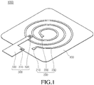
- the magnetic substrate 100 changes the direction of the magnetic field transferred from the transmission side in the lateral direction such that the magnetic field can be more concentrated onto the coil unit 200.
- the first connection terminal 310 of the connecting unit 300 may be connected to the first connection terminal 210 of the coil unit 200 and the second connection terminal 320 of the connecting unit 300 may be connected to the second connection terminal 220 of the coil unit 200.
- the terminal may include a typical mobile phone, such as a cellular phone, a PCS (personal communication service) phone, a GSM phone, a CDMA-2000 phone, or a WCDMA phone, a PMP (portable multimedia player), a PDA (personal digital assistant), a smart phone, or an MBS (mobile broadcast system) phone, but the embodiment is not limited thereto.
- a typical mobile phone such as a cellular phone, a PCS (personal communication service) phone, a GSM phone, a CDMA-2000 phone, or a WCDMA phone, a PMP (portable multimedia player), a PDA (personal digital assistant), a smart phone, or an MBS (mobile broadcast system) phone, but the embodiment is not limited thereto.
- Various devices can be used as the terminal if they can wirelessly receive the power.
- the structure of the wireless power receiver 1000 may be essentially identical to the structure of the wireless power receiver 1000 described with reference to FIGS. 1 to 3 .
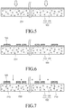
- the structure shown in FIG. 6 is immersed in an etchant so that portions of the conductor 201 where the mask 500 is not positioned may be etched.
- the conductor 201 may have a predetermined conductive pattern.
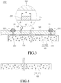
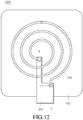
- FIG. 9 is a sectional view taken along line A-A' of the connecting unit 300 of the wireless power receiver 1000 shown in FIG. 2 according to the second embodiment.
- the magnetic substrate 100, the coil unit 200, and the connecting unit 300 are identical to those described with reference to FIG. 1 .
- the wireless power receiver 1000 may include a magnetic substrate 100, a coil unit 200, a connecting unit 300 and a short-range communication antenna 600.
- the first connection terminal 610 and the second connection terminal 620 of the short-range communication antenna 600 are connected to the connecting unit 300.
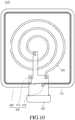
- the short-range communication antenna 600 may be arranged at an outer peripheral portion of the coil unit 200. According to one embodiment, when the coil unit 200 is disposed at the center of the magnetic substrate 100, the short-range communication antenna 600 may be arranged along the outer peripheral portion of the magnetic substrate 100 to surround the coil unit 200.
- the short-range communication antenna 600 may have a rectangular configuration by winding one conductive line several times, but the embodiment is not limited thereto.
- the method of forming the short-range communication antenna 600 on the magnetic substrate 100 may be identical to the method described with reference to FIG. 4 .
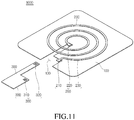
- FIG. 11 is a perspective view illustrating the wireless power receiver 1000 according to the fourth embodiment.
- the wireless power receiver 1000 includes a magnetic substrate 100, a coil unit 200 and a connecting unit 300.
- the connecting unit 300 has a thickness equal to or smaller than a thickness of the magnetic substrate 100.
- the connecting unit 300 may be implemented as a flexible printed circuit board (FPCB).
- the wireless power receiver 1000 can wirelessly receive power from the transmission side using resonance.
- the magnetic substrate 100 can absorb some of the magnetic field received from the transmission side and leaked to the outside to dissipate the magnetic field as heat. If the amount of the magnetic field leaked to the outside is reduced, the bad influence of the magnetic field exerted on the human body can be reduced.
- the support 120 may include thermosetting resin or thermoplastic resin and support the magnetic substrate 100.
- the magnetic substrate 100 may be prepared in the form of a sheet and may have a flexible property.
- the coil unit 200 may be disposed inside the magnetic substrate 100.
- the coil unit 200 may be buried inside the magnetic substrate 100.
- the magnetic substrate 100 may include a pattern groove and the coil unit 200 may be disposed in the pattern groove.
- the pattern groove may be formed as a conductive pattern similar to the coil unit 200.
- a process for manufacturing the wireless power receiver 1000 by disposing the coil unit 200 and the connecting unit 300 in the magnetic substrate 100 will be described later with reference to FIGS. 17 to 21 .
- the first and second connection terminals 210 and 220 of the coil unit 200 are necessary for connection with the connecting unit 300.
- the first connection terminal 310 of the connecting unit 300 may be connected to the first connection terminal 210 of the coil unit 200 and the second connection terminal 320 of the connecting unit 300 may be connected to the second connection terminal 220 of the coil unit 200.
- the printed circuit board 330 may include a wiring layer and the wiring layer may include a wireless power receiving circuit, which will be described later.
- the connecting unit 300 connects the wireless power receiving circuit (not shown) with the coil unit 200 to transfer the power received from the coil unit 200 to a load (not shown) through the wireless power receiver circuit.
- the wireless power receiver circuit may include a rectifier circuit (not shown) for converting AC power into DC power and a smoothing circuit for transferring the DC power to the load after removing ripple components from the DC power.
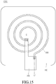
- FIGS. 15 and 16 show the detailed structure of the wireless power receiver 1000 according to the fifth embodiment when the coil unit 200 is connected to the connecting unit 300.
- the via hole can be formed by using a laser.
- the laser may include a UV laser or a CO 2 laser.
- FIG. 16 is a sectional view of the wireless power receiver 1000 in which the magnetic substrate 100 and the coil unit 200 are connected to the connecting unit 300.
- FIGS. 17 to 21 are views for explaining a method of manufacturing the wireless power receiver 1000 according to the fifth embodiment.
- the magnetic substrate 100 is prepared.
- the magnetic substrate 100 may be produced by coating metal powder of sendust alloys, such as Al, Fe and SiO2, on polyethylene rubber and then forming an oxide layer on a surface of the polyethylene rubber.
- the mold 1 may have the shape corresponding to the shape of the coil unit 200.
- the mold 1 can be manufactured by using an aluminum alloy, a copper alloy or a cast iron.
- the heat temperature and pressure may vary depending on the distribution and concentration of the metal powder. That is, if the distribution of the metal powder is not uniform, the higher temperature and pressure may be applied. In contrast, if the distribution of the metal powder is uniform, the lower temperature and pressure may be applied. In addition, if the concentration of the metal powder is low, the lower temperature and pressure may be applied as compared with the case in which the concentration of the metal powder is high. Further, the heat temperature and pressure may vary depending on the composition of the metal powder, that is, depending on the alloy constituting the metal powder.
- laser may be irradiated, instead of applying heat and pressure using the mold 1, to form the pattern groove in the magnetic substrate 100 to receive the coil unit 200.
- the pattern groove can be formed by using an excimer laser that irradiates the laser beam having a wavelength band of ultraviolet ray.
- the excimer laser may include a KrF excimer laser (central wavelength 248 nm) or an ArF excimer laser (central wavelength 193 nm).
- the mold 1 is separated from the magnetic substrate 100 so that the magnetic substrate 100 is formed with the pattern groove 140.
- first connection terminal 210 of the coil unit 200 is connected to the first connection terminal 310 of the connecting unit 300 through the solder 10 and the second connection terminal 220 of the coil unit 200 is connected to the second connection terminal 320 of the connecting unit 300 through the solder 20.
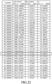
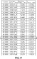
- the inductance of the coil unit 200 is increased by 352.42 um from about 9986.92 um to about 10339.34 um and the resistance of the coil unit 200 is reduced by 0.057 ⁇ from 0.910 ⁇ to 0.853 ⁇ . That is, the Q value is increased corresponding to the increment of the inductance and the reduction of the resistance.
- FIG. 24 is an H-field for illustrating a radiation pattern of a magnetic field when the coil unit is disposed on a top surface of the magnetic substrate according to the first embodiment
- FIG. 25 is an H-field for illustrating a radiation pattern of a magnetic field when the coil unit is disposed in the pattern groove formed in the magnetic substrate according to the fifth embodiment.
- a greater amount of magnetic fields is radiated from the outer peripheral portion of the coil unit 200 when the coil unit 200 is disposed in the pattern groove formed in the magnetic substrate 100 as compared with the case in which the coil unit 200 is disposed on the top surface of the magnetic substrate 100. This is because the magnetic field directed to the outside is changed in the lateral direction of the coil unit 200 due to the coil unit 200 buried in the magnetic substrate 100.
- a greater amount of magnetic fields is radiated at the inner portion of the coil unit 200 when the coil unit 200 is disposed in the pattern groove formed in the magnetic substrate 100 as compared with the case in which the coil unit 200 is disposed on the top surface of the magnetic substrate 100. This is also because the magnetic field directed to the outside is changed in the lateral direction of the coil unit 200 due to the coil unit 200 buried in the magnetic substrate 100.
- the wireless power receiver 1000 may further include a short-range communication antenna 600.
- the short-range communication antenna 600 can make near field communication with a reader.
- the short-range communication antenna 600 may serve as an antenna that transceives information in cooperation with the reader.
- the short-range communication antenna 600 may be arranged at an outer peripheral portion of the coil unit 200. According to one embodiment, when the coil unit 200 is disposed at the center of the magnetic substrate 100, the short-range communication antenna 600 may be arranged along the outer peripheral portion of the magnetic substrate 100 to surround the coil unit 200.
- the short-range communication antenna 600 may have a rectangular configuration by winding one conductive line several times, but the embodiment is not limited thereto.
- the short-range communication antenna 600 may be formed as a conductive pattern for example a conductive layer.
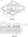
- FIG. 27 is a perspective view showing the assembled state of the elements of the wireless power receiver 1000 shown in FIG. 26 , in which some elements are omitted.
- the magnetic substrate 100 can change the direction of the magnetic field transferred from the transmission side.
- the magnetic substrate 100 changes the direction of the magnetic field transferred to the coil unit 200 from the transmission side to reduce the amount of the magnetic field leaked to the outside.
- the magnetic substrate 100 may have the electromagnetic wave shielding effect.
- the magnetic substrate 100 changes the direction of the magnetic field transferred from the transmission side in the lateral direction such that the magnetic field can be more concentrated onto the coil unit 200.
- the magnetic substrate 100 can absorb some of the magnetic field transferred to the coil unit 200 from the transmission side and leaked to the outside to dissipate the magnetic field as heat. If the amount of the magnetic field leaked to the outside is reduced, the bad influence of the magnetic field exerted on the human body can be reduced.
- the magnetic substrate 100 may include a magnet 110 and a support 120.
- the support 120 may include thermosetting resin or thermoplastic resin and support the magnetic substrate 100.
- the magnetic substrate 100 may be prepared in the form of a sheet and may have a flexible property.
- a receiving space 130 is formed at a predetermined area of the magnet substrate 100.
- the receiving space 130 has a structure the same as that of the connecting unit 300.
- the connecting unit 300 is disposed in the receiving space 130 and connected to the coil unit 200.
- the connecting unit 300 connects a receiver circuit (not shown) with the coil unit 200 to transfer the power received from the coil unit 200 to a load (not shown) through the receiver circuit.
- the connecting unit 300 may include a wiring layer and the wiring layer may include the wireless power receiving circuit.
- the wireless power receiving circuit may include a rectifier circuit for rectifying the power received from the coil unit 200, a smoothing circuit for removing noise signals, and a main IC chip for performing the operation to wirelessly receive the power.
- the receiver circuit can transfer the signal received from the short-range communication antenna 600 to an short-range communication signal processing unit (not shown).
- the connecting unit 300 is disposed in the receiving space 130 of the magnetic substrate 100 and connected to the coil unit 200.
- FIG. 27 shows the connecting unit 300 disposed in the receiving space 130 of the magnetic substrate 100.
- the connecting unit 300 may have the shape corresponding to the shape of the receiving space 130 and may be disposed in the receiving space 130. Since the connecting unit 300 is disposed in the receiving space 130 of the magnetic substrate 100, the thickness of the wireless power receiver 1000 can be remarkably reduced as much as the thickness of the connecting unit 300. Thus, the thickness of the electronic device, such as a portable terminal, equipped with the wireless power receiver 1000 can be remarkably reduced.
- the connecting unit 300 may include a flexible printed circuit board (FPCB), a tape substrate (TS) or a lead frame (LF). If the tape substrate is used as the connecting unit 300, the thickness of the connecting unit 300 can be reduced, so that the overall size of the wireless power receiver 1000 can be reduced.
- FPCB flexible printed circuit board
- TS tape substrate
- LF lead frame
- the wiring layer included in the connecting unit 300 can be protected from the heat, external moisture or impact and the mass production can be realized.
- the short-range communication antenna 600 can make near field communication with a reader.
- the short-range communication antenna 600 may serve as an antenna that transceives information in cooperation with the reader.
- the NFC signal processing unit (not shown) can process the signal transferred to the short-range communication antenna 600 through the connecting unit 300.
- the short-range communication antenna 600 may be arranged at an outer peripheral portion of the coil unit 200. Referring to FIG. 27 , when the coil unit 200 is disposed at the magnetic substrate 100, the short-range communication antenna 600 may be arranged along the outer peripheral portion of the magnetic substrate 100 to surround the coil unit 200.
- the short-range communication antenna 600 may have a rectangular configuration by winding one conductive line several times, but the embodiment is not limited thereto.
- the second dual-side adhesive layer 720 adheres the protective film 800 to the release paper layer 730, which will be described later in detail.
- the coil unit 200 may be disposed on the magnetic substrate 100 and may have a spiral structure, but the embodiment is not limited thereto.
- the conductor 201 may be formed by using an alloy including copper.
- the copper is in the form of roll annealed copper or electrodeposited copper.
- the conductor 201 may have various thicknesses depending on the specification of a product. According to one embodiment, the conductor 201 may have the thickness of 100 ⁇ m, but the embodiment is not limited thereto.
- the adhesive layer 700 is used to reinforce the adhesive strength between the conductor 201 and the protective film 800.
- the adhesive layer 700 may include thermosetting resin, but the embodiment is not limited thereto.
- the adhesive layer may have the thickness of 17 ⁇ m, but the embodiment is not limited thereto.
- the conductor 201 is formed on the protective film 800 by the adhesive layer 700.
- the laminating process can be used to form the conductor 201 on the protective film 800.
- the laminating process refers to the process to bond heterogeneous materials with each other by applying predetermined heat and pressure.
- a photoresist film 900 is attached onto the top surface of the conductor 201.
- the photoresist film 900 is used for etching the conductor 201 to form a predetermined conductive pattern in the conductor 201.
- a UV exposure type film or an LDI exposure type film may be used as the photoresist film 900.
- a photoresist coating solution can be coated on the top surface of the conductor 201 without using the photoresist film 900.
- the mask pattern 910 may be formed on the top surface of the conductor 201 corresponding to the position of the conductive pattern.
- the mask pattern 910 may be formed in the regions corresponding to the coil unit 200 and the short-range communication antenna 600.
- the conductor 201 exposed through the mask pattern 910 may be etched.
- the soldering process is performed to connect the coil unit 200 and the short-range communication antenna 600 to the connecting unit 300.
- the soldering process includes the reflow process, but the embodiment is not limited thereto.
- the reflow process refers to the process for bonding the coil unit 230 and the short-range communication antenna 600 with the connecting unit 300 by melting solder cream using high-temperature heat to ensure the stable electrical connection between the connecting unit 300 and the coil unit 230/NFC antenna 600.
- the first connection terminal 310 of the connecting unit 300 may be connected to the first connection terminal 210 of the coil unit 200 by a solder 30, the second connection terminal 320 of the connecting unit 300 may be connected to the second connection terminal 220 of the coil unit 200 by the solder 30, the third connection terminal 340 of the connecting unit 300 may be connected to the first connection terminal 610 of the short-range communication antenna 600 by the solder 30 and the fourth connection terminal 350 of the connecting unit 300 may be connected to the second connection terminal 620 of the short-range communication antenna 600.
- the thickness of the wireless power receiver 1000 can be remarkably reduced as much as the thickness of the connecting unit 300.
- the thickness of the electronic device, such as a portable terminal, equipped with the wireless power receiver 1000 can be remarkably reduced.
- the coil 230/short-range communication antenna 600 and the magnetic substrate 100 may be adhered with each other by the first dual-side adhesive layer 710.
- the magnetic substrate 100 may have the thickness in the range of 100 ⁇ m to 800 ⁇ m, but the embodiment is not limited thereto.
- the first dual-side adhesive layer 710 may have the thickness in the range of 10 ⁇ m to 50 ⁇ m, but the embodiment is not limited thereto.
Landscapes
- Engineering & Computer Science (AREA)
- Power Engineering (AREA)
- Computer Networks & Wireless Communication (AREA)
- Signal Processing (AREA)
- Physics & Mathematics (AREA)
- Computer Hardware Design (AREA)
- Microelectronics & Electronic Packaging (AREA)
- General Physics & Mathematics (AREA)
- Theoretical Computer Science (AREA)
- Manufacturing & Machinery (AREA)
- Electromagnetism (AREA)
- Transportation (AREA)
- Mechanical Engineering (AREA)
- Coils Or Transformers For Communication (AREA)
- Near-Field Transmission Systems (AREA)
- Parts Printed On Printed Circuit Boards (AREA)
- Manufacturing Cores, Coils, And Magnets (AREA)
- Charge And Discharge Circuits For Batteries Or The Like (AREA)
Applications Claiming Priority (3)
| Application Number | Priority Date | Filing Date | Title |
|---|---|---|---|
| KR20120029987 | 2012-03-23 | ||
| KR20120079004 | 2012-07-19 | ||
| EP12190583.0A EP2642632B1 (fr) | 2012-03-23 | 2012-10-30 | Récepteur de puissance sans fil et son procédé de fabrication |
Related Parent Applications (2)
| Application Number | Title | Priority Date | Filing Date |
|---|---|---|---|
| EP12190583.0A Division-Into EP2642632B1 (fr) | 2012-03-23 | 2012-10-30 | Récepteur de puissance sans fil et son procédé de fabrication |
| EP12190583.0A Division EP2642632B1 (fr) | 2012-03-23 | 2012-10-30 | Récepteur de puissance sans fil et son procédé de fabrication |
Publications (3)
| Publication Number | Publication Date |
|---|---|
| EP3174173A2 true EP3174173A2 (fr) | 2017-05-31 |
| EP3174173A3 EP3174173A3 (fr) | 2017-09-06 |
| EP3174173B1 EP3174173B1 (fr) | 2021-03-03 |
Family
ID=47598569
Family Applications (3)
| Application Number | Title | Priority Date | Filing Date |
|---|---|---|---|
| EP12190583.0A Active EP2642632B1 (fr) | 2012-03-23 | 2012-10-30 | Récepteur de puissance sans fil et son procédé de fabrication |
| EP16206292.1A Active EP3174173B1 (fr) | 2012-03-23 | 2012-10-30 | Récepteur de puissance sans fil et son procédé de fabrication |
| EP17157643.2A Active EP3193423B1 (fr) | 2012-03-23 | 2012-10-30 | Récepteur de puissance sans fil et son procédé de fabrication |
Family Applications Before (1)
| Application Number | Title | Priority Date | Filing Date |
|---|---|---|---|
| EP12190583.0A Active EP2642632B1 (fr) | 2012-03-23 | 2012-10-30 | Récepteur de puissance sans fil et son procédé de fabrication |
Family Applications After (1)
| Application Number | Title | Priority Date | Filing Date |
|---|---|---|---|
| EP17157643.2A Active EP3193423B1 (fr) | 2012-03-23 | 2012-10-30 | Récepteur de puissance sans fil et son procédé de fabrication |
Country Status (6)
| Country | Link |
|---|---|
| US (4) | US9806565B2 (fr) |
| EP (3) | EP2642632B1 (fr) |
| JP (4) | JP5805609B2 (fr) |
| KR (1) | KR101417388B1 (fr) |
| CN (2) | CN104638778B (fr) |
| TW (3) | TWI459418B (fr) |
Families Citing this family (61)
| Publication number | Priority date | Publication date | Assignee | Title |
|---|---|---|---|---|
| US11329511B2 (en) | 2006-06-01 | 2022-05-10 | Mojo Mobility Inc. | Power source, charging system, and inductive receiver for mobile devices |
| WO2013141658A1 (fr) * | 2012-03-23 | 2013-09-26 | 엘지이노텍 주식회사 | Ensemble antenne et son procédé de fabrication |
| TWI459418B (zh) * | 2012-03-23 | 2014-11-01 | Lg伊諾特股份有限公司 | 無線功率接收器以及包含有其之可攜式終端裝置 |
| JP2013214909A (ja) * | 2012-04-03 | 2013-10-17 | Denso Corp | 車両用携帯機 |
| CN109067014B (zh) * | 2012-09-05 | 2022-04-15 | 瑞萨电子株式会社 | 非接触充电装置 |
| KR102019080B1 (ko) * | 2012-12-13 | 2019-11-04 | 엘지이노텍 주식회사 | 무선전력 수신장치 및 그의 제조 방법 |
| KR101452093B1 (ko) * | 2013-03-13 | 2014-10-16 | 삼성전기주식회사 | 박막 코일, 이를 포함하는 차폐 부재 및 이를 구비하는 무접점 전력 전송 장치 |
| JP6395304B2 (ja) | 2013-11-13 | 2018-09-26 | ローム株式会社 | 半導体装置および半導体モジュール |
| KR20160096085A (ko) * | 2013-12-10 | 2016-08-12 | 쥬코쿠 덴료쿠 가부시키 가이샤 | 송전 장치, 급전 시스템 |
| KR20150089754A (ko) * | 2014-01-28 | 2015-08-05 | 엘지이노텍 주식회사 | 무선 전력 수신 장치 및 단말기 |
| JP2015144160A (ja) * | 2014-01-31 | 2015-08-06 | デクセリアルズ株式会社 | アンテナ装置、非接触電力伝送用アンテナユニット、電子機器 |
| JP2015149405A (ja) * | 2014-02-06 | 2015-08-20 | デクセリアルズ株式会社 | アンテナ装置、非接触電力伝送用アンテナユニット、及び電子機器 |
| CN104078759A (zh) * | 2014-06-27 | 2014-10-01 | 南通富士通微电子股份有限公司 | 射频识别天线的形成方法 |
| US9520648B2 (en) * | 2014-07-23 | 2016-12-13 | Mediatek Inc. | Polygon near field communication antenna |
| KR102152653B1 (ko) * | 2014-08-18 | 2020-09-08 | 엘지이노텍 주식회사 | 무선 전력 수신 장치 |
| KR102118352B1 (ko) * | 2015-01-07 | 2020-06-04 | 삼성전자주식회사 | 무선 전력 수신기 |
| WO2016111554A1 (fr) | 2015-01-07 | 2016-07-14 | Samsung Electronics Co., Ltd. | Récepteur d'énergie sans fil |
| CN105633565A (zh) * | 2015-01-14 | 2016-06-01 | 宇龙计算机通信科技(深圳)有限公司 | Nfc天线的制造方法、用于移动终端的电池盖及移动终端 |
| KR20160089168A (ko) * | 2015-01-19 | 2016-07-27 | 주식회사 아모센스 | 안테나 장치, 그의 제조 방법 및 그를 구비한 전자기기 |
| KR20170005670A (ko) | 2015-07-06 | 2017-01-16 | 엘지이노텍 주식회사 | 무선 충전과 nfc 통신을 위한 무선 안테나 및 이를 적용한 무선 단말기 |
| CN106488654A (zh) * | 2015-08-27 | 2017-03-08 | 全亿大科技(佛山)有限公司 | 线圈载板的制造方法 |
| KR101899476B1 (ko) * | 2015-10-21 | 2018-09-18 | 주식회사 이엠따블유 | 무선 충전 모듈 및 이를 구비하는 모바일 단말기 |
| KR20170050656A (ko) * | 2015-10-30 | 2017-05-11 | 삼성전자주식회사 | 무선 전력 수신기 및 그 제어 방법 |
| KR102030704B1 (ko) * | 2015-11-05 | 2019-10-10 | 주식회사 아모텍 | 콤보형 안테나 모듈 |
| CN105304312B (zh) * | 2015-11-25 | 2017-11-21 | 上海安费诺永亿通讯电子有限公司 | 一种无线充电线圈的制作方法及无线充电线圈 |
| KR101804410B1 (ko) | 2015-12-17 | 2017-12-04 | 엘지이노텍 주식회사 | 무선 전력 송신기를 위한 송신 코일 모듈 |
| KR102484849B1 (ko) * | 2015-12-18 | 2023-01-05 | 주식회사 위츠 | 코일 조립체 |
| KR102527794B1 (ko) * | 2016-02-04 | 2023-05-03 | 삼성전자주식회사 | 코일을 포함하는 전자 장치 |
| KR102579117B1 (ko) * | 2016-02-05 | 2023-09-15 | 삼성전자주식회사 | 무선 충전 장치 |
| CN105813183B (zh) * | 2016-04-20 | 2019-03-26 | 深圳市速腾聚创科技有限公司 | 一种带能量传输的无线通信系统 |
| KR102560030B1 (ko) | 2016-05-27 | 2023-07-26 | 삼성전자주식회사 | 무선 전력 수신기 및 그 방법 |
| KR20190038587A (ko) * | 2016-08-26 | 2019-04-08 | 누커런트, 인코포레이티드 | 무선 커넥터 시스템 |
| KR20180042578A (ko) * | 2016-10-18 | 2018-04-26 | 엘지이노텍 주식회사 | 무선전력 송신 장치 |
| KR101862690B1 (ko) * | 2016-10-20 | 2018-07-05 | 한국철도기술연구원 | 무선전력전송용 인쇄회로기판 타입 코일 |
| KR101897879B1 (ko) * | 2016-12-29 | 2018-09-13 | 주식회사 켐트로닉스 | 무선충전기용 tx 코일 구조체 |
| CN106887325B (zh) * | 2017-02-20 | 2018-08-21 | 北京博瑞莱智能科技集团有限公司 | 调容变压器低压箔绕线圈加工工艺 |
| CN110383959B (zh) * | 2017-03-08 | 2023-03-24 | 住友电工印刷电路株式会社 | 柔性印刷电路板 |
| KR102542787B1 (ko) | 2017-03-17 | 2023-06-14 | 이피션트 파워 컨버젼 코퍼레이션 | 대면적 확장 가능한 고 공진 무선 전력 코일 |
| US11177680B2 (en) * | 2017-04-04 | 2021-11-16 | Intel Corporation | Field shaper for a wireless power transmitter |
| CN107492440A (zh) * | 2017-09-20 | 2017-12-19 | 成都瑞德星无线技术有限公司 | 一种具有电磁屏蔽效能的无线电能传输装置 |
| TWI740091B (zh) * | 2018-01-12 | 2021-09-21 | 乾坤科技股份有限公司 | 電子裝置及其製作方法 |
| US11011461B2 (en) * | 2018-02-12 | 2021-05-18 | Qualcomm Incorporated | Perpendicular inductors integrated in a substrate |
| JP7063668B2 (ja) * | 2018-03-22 | 2022-05-09 | ホシデン株式会社 | コイル、無接点給電ユニット、及びコイルの製造方法 |
| CN111566889B (zh) * | 2018-05-25 | 2024-02-02 | Oppo广东移动通信有限公司 | 无线充电接收装置及移动终端 |
| EP3786988A4 (fr) * | 2018-06-11 | 2021-09-01 | Guangdong Oppo Mobile Telecommunications Corp., Ltd. | Bobine de charge sans fil, ensemble de charge sans fil et dispositif électronique |
| CN108806967B (zh) * | 2018-06-12 | 2020-08-25 | 上海安费诺永亿通讯电子有限公司 | 一种无线充电线圈的制作方法及结构 |
| JP2019220908A (ja) * | 2018-06-22 | 2019-12-26 | アズビル株式会社 | 電子機器およびnfcアンテナ |
| CN109088162B (zh) * | 2018-08-17 | 2024-02-20 | 深圳市嘉姆特科技有限公司 | 散热及辐射兼用无线通信天线结构 |
| JP7175988B2 (ja) * | 2018-08-29 | 2022-11-21 | 新電元工業株式会社 | コイル装置 |
| KR102127207B1 (ko) * | 2018-09-05 | 2020-06-29 | 주식회사 지유니슨 | 플렉서블 코일 및 그 제조 방법 |
| US10855111B2 (en) * | 2018-12-07 | 2020-12-01 | Ming Chung TSANG | Wireless charging coil apparatus |
| US11387678B2 (en) * | 2019-09-27 | 2022-07-12 | Apple Inc. | Stacked resonant structures for wireless power systems |
| CN110838617A (zh) * | 2019-11-13 | 2020-02-25 | 铜川煜力机械制造有限公司 | 一种应力天线、制备方法及应用 |
| KR20210115262A (ko) * | 2020-03-12 | 2021-09-27 | 엘지이노텍 주식회사 | 손떨림 보정을 위한 코일 기판 및 이를 포함하는 카메라 모듈 |
| CN112039560B (zh) * | 2020-08-28 | 2022-07-26 | 武汉天马微电子有限公司 | 一种穿戴显示模组和穿戴显示装置 |
| KR20220036756A (ko) * | 2020-09-16 | 2022-03-23 | 삼성전자주식회사 | 코일 안테나를 포함하는 전자 장치 |
| KR20220055762A (ko) * | 2020-10-27 | 2022-05-04 | 쓰리엠 이노베이티브 프로퍼티즈 캄파니 | 코일 및 이를 포함하는 전력 시스템 |
| JP7016200B1 (ja) * | 2020-10-30 | 2022-02-04 | 株式会社フェニックスソリューション | ゴム製品用rfidタグ及びゴム製品用rfidタグの製造方法 |
| CN112735769B (zh) * | 2020-12-23 | 2022-07-15 | 上海安费诺永亿通讯电子有限公司 | 一种铝fpc型线圈结构及其制造方法 |
| JP2022117331A (ja) * | 2021-01-29 | 2022-08-10 | ブラザー工業株式会社 | インクジェットプリンタ |
| CN214672190U (zh) * | 2021-02-03 | 2021-11-09 | 华为技术有限公司 | 线圈模组、线圈封装结构及无线充电装置 |
Family Cites Families (180)
| Publication number | Priority date | Publication date | Assignee | Title |
|---|---|---|---|---|
| JPS5678415U (fr) | 1979-11-14 | 1981-06-25 | ||
| JPS6169811A (ja) | 1984-09-12 | 1986-04-10 | Mitsubishi Chem Ind Ltd | 安定剤を含有する高分子量3メチルブテン−1重合体 |
| JPS6169811U (fr) * | 1984-10-12 | 1986-05-13 | ||
| US4947180A (en) * | 1989-06-14 | 1990-08-07 | Terk Technologies Corporation | FM antenna |
| JPH0451115U (fr) | 1990-08-31 | 1992-04-30 | ||
| JPH0479408U (fr) * | 1990-11-22 | 1992-07-10 | ||
| JPH06267746A (ja) | 1993-03-09 | 1994-09-22 | Murata Mfg Co Ltd | ノイズ除去部品 |
| JPH0774038A (ja) | 1993-09-02 | 1995-03-17 | Tdk Corp | ロータリートランスの製造方法 |
| JPH0879976A (ja) | 1994-09-07 | 1996-03-22 | Tdk Corp | 非接触型充電器 |
| US5574470A (en) | 1994-09-30 | 1996-11-12 | Palomar Technologies Corporation | Radio frequency identification transponder apparatus and method |
| JPH10282232A (ja) | 1997-03-31 | 1998-10-23 | Toshiba Corp | 無線通信システム |
| JPH11103531A (ja) * | 1997-09-29 | 1999-04-13 | Nec Mori Energy Kk | 非接触充電装置 |
| JPH11175676A (ja) | 1997-12-12 | 1999-07-02 | Hitachi Maxell Ltd | 非接触式icカード |
| JP2001027687A (ja) | 1999-07-14 | 2001-01-30 | Ishikawajima Harima Heavy Ind Co Ltd | ベント管ベローズ点検装置 |
| FR2800518B1 (fr) * | 1999-10-28 | 2007-02-23 | A S K | Antenne de couplage a inductance elevee |
| FR2814574B1 (fr) | 2000-09-22 | 2003-11-28 | Gemplus Card Int | Etiquette electronique sans contact pour produit a surface conductrice |
| JP2002299138A (ja) * | 2001-04-02 | 2002-10-11 | Kawasaki Steel Corp | 非接触充電器用平面磁気素子 |
| US7463154B2 (en) | 2001-04-30 | 2008-12-09 | Neology, Inc. | Selective metal removal process for metallized retro-reflective and holographic films and radio frequency devices made therewith |
| EP1315234A1 (fr) | 2001-11-26 | 2003-05-28 | Eta SA Fabriques d'Ebauches | Antenne de réception d'ondes VHF logée dans un bracelet de dispositif électronique portable |
| JP3815337B2 (ja) | 2002-01-28 | 2006-08-30 | 株式会社デンソーウェーブ | 非接触式icカード |
| JP3919100B2 (ja) | 2002-10-29 | 2007-05-23 | ソニー・エリクソン・モバイルコミュニケーションズ株式会社 | 携帯通信端末 |
| KR20040063286A (ko) | 2003-01-06 | 2004-07-14 | 미창테크 주식회사 | 에나멜 코일 안테나 및 그 제조 방법 |
| JP3870921B2 (ja) * | 2003-04-01 | 2007-01-24 | セイコーエプソン株式会社 | 非接触識別タグ |
| US8026819B2 (en) | 2005-10-02 | 2011-09-27 | Visible Assets, Inc. | Radio tag and system |
| JP2004364199A (ja) | 2003-06-06 | 2004-12-24 | Sony Corp | アンテナモジュール及びこれを備えた携帯型通信端末 |
| JP4170165B2 (ja) | 2003-06-30 | 2008-10-22 | Tdk株式会社 | 反応性イオンエッチング用のマスク材料、マスク及びドライエッチング方法 |
| JP2005080023A (ja) | 2003-09-01 | 2005-03-24 | Sony Corp | 磁芯部材、アンテナモジュール及びこれを備えた携帯型通信端末 |
| KR100998039B1 (ko) | 2003-10-01 | 2010-12-03 | 삼성테크윈 주식회사 | 기판 제조 방법 및 이를 이용하여 제조된 스마트 라벨 |
| JP2005117354A (ja) | 2003-10-08 | 2005-04-28 | Nec Saitama Ltd | 携帯電話機及びそれに用いる電池パック並びに接続コネクタ |
| US7006051B2 (en) | 2003-12-02 | 2006-02-28 | Frc Components Products Inc. | Horizontally polarized omni-directional antenna |
| JP3834033B2 (ja) | 2003-12-24 | 2006-10-18 | 株式会社東芝 | 無線カード |
| US7791440B2 (en) | 2004-06-09 | 2010-09-07 | Agency For Science, Technology And Research | Microfabricated system for magnetic field generation and focusing |
| KR20050120481A (ko) | 2004-06-19 | 2005-12-22 | 삼성테크윈 주식회사 | 전자 무선 인식 장치 및 전자 무선 인식 장치의 제조방법 |
| JP4852829B2 (ja) | 2004-07-28 | 2012-01-11 | セイコーエプソン株式会社 | 非接触電力伝送装置 |
| WO2006011656A1 (fr) | 2004-07-28 | 2006-02-02 | Matsushita Electric Industrial Co., Ltd. | Appareil d'antenne |
| KR20040072581A (ko) | 2004-07-29 | 2004-08-18 | (주)제이씨 프로텍 | 전자기파 증폭중계기 및 이를 이용한 무선전력변환장치 |
| JP2006050265A (ja) * | 2004-08-04 | 2006-02-16 | Sony Corp | アンテナモジュール用磁芯部材、アンテナモジュールおよびこれを備えた携帯情報端末 |
| US20070007661A1 (en) | 2005-06-09 | 2007-01-11 | Burgess Lester E | Hybrid conductive coating method for electrical bridging connection of RFID die chip to composite antenna |
| US7685706B2 (en) | 2005-07-08 | 2010-03-30 | Semiconductor Energy Laboratory Co., Ltd | Method of manufacturing a semiconductor device |
| CN2888666Y (zh) | 2005-11-14 | 2007-04-11 | 北京握奇数据系统有限公司 | 供插入式智能卡非接触界面使用的天线组件 |
| KR101052981B1 (ko) | 2006-03-24 | 2011-07-29 | 도시바 마테리알 가부시키가이샤 | 비접촉형의 수전 장치와 그것을 이용한 전자 기기 및 비접촉 충전 장치 |
| US7923719B2 (en) | 2006-04-28 | 2011-04-12 | Semiconductor Energy Laboratory Co., Ltd. | Semiconductor memory device wherein wiring contact is made through an opening in an organic compound layer |
| JP2007311407A (ja) | 2006-05-16 | 2007-11-29 | Dainippon Printing Co Ltd | Icチップ、回路形成済ウエハ、および非接触通信部材 |
| US7948208B2 (en) | 2006-06-01 | 2011-05-24 | Mojo Mobility, Inc. | Power source, charging system, and inductive receiver for mobile devices |
| JP2008027015A (ja) * | 2006-07-19 | 2008-02-07 | Dainippon Printing Co Ltd | 非接触icカード |
| JP4466689B2 (ja) | 2006-08-31 | 2010-05-26 | 株式会社カシオ日立モバイルコミュニケーションズ | アンテナ及び携帯電子機器 |
| JP5052079B2 (ja) | 2006-09-08 | 2012-10-17 | 株式会社半導体エネルギー研究所 | センサ装置及びそれを有する容器類 |
| US7971339B2 (en) | 2006-09-26 | 2011-07-05 | Hid Global Gmbh | Method and apparatus for making a radio frequency inlay |
| FR2908541B1 (fr) | 2006-11-06 | 2009-01-16 | Id3S Identification Solutions | Dispositif d'identification par radiofrequence et procede de realisation d'un tel dispositif |
| JP4422712B2 (ja) | 2006-11-21 | 2010-02-24 | 株式会社スマート | 共振器付フィールド改善システム |
| JP2008135589A (ja) | 2006-11-29 | 2008-06-12 | Asuka Electron Kk | 電力伝送用コイル |
| JP4404088B2 (ja) | 2006-11-30 | 2010-01-27 | Tdk株式会社 | コイル部品 |
| WO2008070524A2 (fr) | 2006-12-01 | 2008-06-12 | Tti Ellebeau, Inc. | Systèmes, dispositifs et procédés permettant d'alimenter et/ou de contrôler des dispositifs, par exemple des dispositifs d'application transdermique |
| JP4947637B2 (ja) | 2007-01-09 | 2012-06-06 | ソニーモバイルコミュニケーションズ株式会社 | 無接点電力伝送コイル、携帯端末及び端末充電装置 |
| KR100867405B1 (ko) | 2007-02-09 | 2008-11-06 | (주)애니쿼터스 | Rfid 리더기의 무선 주파수를 이용한 이동 통신 단말기배터리 충전 장치 |
| KR100900476B1 (ko) | 2007-02-16 | 2009-06-03 | 삼성전자주식회사 | 이동통신 단말기 및 그것의 배터리 충전 방법 |
| JP4412402B2 (ja) * | 2007-02-20 | 2010-02-10 | セイコーエプソン株式会社 | コイルユニット及び電子機器 |
| US8022801B2 (en) * | 2007-02-20 | 2011-09-20 | Seiko Epson Corporation | Coil unit and electronic instrument |
| JP2008205215A (ja) | 2007-02-20 | 2008-09-04 | Seiko Epson Corp | 積層コイルユニット並びにそれを用いた電子機器及び充電器 |
| JP2008210861A (ja) | 2007-02-23 | 2008-09-11 | Yonezawa Densen Kk | 防磁シート付きコイル |
| US8009101B2 (en) | 2007-04-06 | 2011-08-30 | Murata Manufacturing Co., Ltd. | Wireless IC device |
| JP5121307B2 (ja) | 2007-05-28 | 2013-01-16 | ソニーモバイルコミュニケーションズ株式会社 | 無接点電力伝送コイルユニット、携帯端末、送電装置、及び、無接点電力伝送システム |
| TW200905703A (en) | 2007-07-27 | 2009-02-01 | Delta Electronics Inc | Magnetic device and manufacturing method thereof |
| US8078226B2 (en) | 2007-08-29 | 2011-12-13 | Mxtran, Inc. | Multiple interface card in a mobile phone |
| JP2009065388A (ja) * | 2007-09-05 | 2009-03-26 | Toshiba Corp | 無線装置及びアンテナ装置 |
| KR100928119B1 (ko) | 2007-10-30 | 2009-11-24 | 삼성에스디아이 주식회사 | 인쇄회로 기판과 이를 이용한 이차전지 |
| US7926728B2 (en) | 2007-10-31 | 2011-04-19 | Infineon Technologies Ag | Integrated circuit device including a contactless integrated circuit inlay |
| TWI349394B (en) * | 2007-11-01 | 2011-09-21 | Asustek Comp Inc | Antenna device |
| JP2009158598A (ja) | 2007-12-25 | 2009-07-16 | Panasonic Electric Works Co Ltd | 平面コイル及びこれを用いた非接触電力伝送機器 |
| US20110050164A1 (en) | 2008-05-07 | 2011-03-03 | Afshin Partovi | System and methods for inductive charging, and improvements and uses thereof |
| US20120248981A1 (en) * | 2008-09-27 | 2012-10-04 | Aristeidis Karalis | Multi-resonator wireless energy transfer for lighting |
| US8487480B1 (en) * | 2008-09-27 | 2013-07-16 | Witricity Corporation | Wireless energy transfer resonator kit |
| US8624546B2 (en) * | 2008-12-12 | 2014-01-07 | Hanrim Postech Co., Ltd. | Non-contact power reception apparatus and jig for fabricating core for non-contact power reception apparatus |
| US8739402B2 (en) | 2008-12-17 | 2014-06-03 | Microconnections Sas | Method of manufacture of IC contactless communication devices |
| US8188933B2 (en) | 2008-12-17 | 2012-05-29 | Panasonic Corporation | Antenna unit and mobile terminal therewith |
| US9312924B2 (en) | 2009-02-10 | 2016-04-12 | Qualcomm Incorporated | Systems and methods relating to multi-dimensional wireless charging |
| JP5316638B2 (ja) | 2009-03-13 | 2013-10-16 | 株式会社村田製作所 | アンテナ装置 |
| US20100265041A1 (en) * | 2009-04-16 | 2010-10-21 | Powerid Ltd. | Rfid transponder |
| EP2433347B1 (fr) | 2009-05-20 | 2013-10-23 | Koninklijke Philips N.V. | Dispositif électronique comprenant bobine inductive de reception avec couche-écran ultra-mince et procédé |
| KR101079679B1 (ko) | 2009-06-03 | 2011-11-04 | 동양미래대학 산학협력단 | 비접촉 전원 충전장치 |
| US20100308187A1 (en) | 2009-06-04 | 2010-12-09 | Pi-Fen Lin | Integrated magnetic device and a magnetic board thereof |
| CN101924398A (zh) | 2009-06-11 | 2010-12-22 | 陈重佑 | 电子锁的非接触式充电装置 |
| JP4788850B2 (ja) | 2009-07-03 | 2011-10-05 | 株式会社村田製作所 | アンテナモジュール |
| US20110032685A1 (en) * | 2009-08-07 | 2011-02-10 | Sony Corporation | Interposer, module, and electronics device including the same |
| JP2011066627A (ja) | 2009-09-16 | 2011-03-31 | Smart:Kk | Nfcセンサアンテナ |
| JP2011097534A (ja) | 2009-11-02 | 2011-05-12 | Tokai Rika Co Ltd | クレードルの態様自動変更装置 |
| KR101086828B1 (ko) | 2009-11-30 | 2011-11-25 | 엘지이노텍 주식회사 | 매립형 인쇄회로기판, 다층 인쇄회로기판 및 이들의 제조방법 |
| KR101538835B1 (ko) | 2010-01-25 | 2015-07-22 | 아사히 가라스 가부시키가이샤 | 적층체의 제조 방법 및 적층체 |
| US8648757B2 (en) | 2010-04-30 | 2014-02-11 | Raytheon Company | End-loaded topology for D-plane polarization improvement |
| US20110285494A1 (en) | 2010-05-24 | 2011-11-24 | Samsung Electro-Mechanics Co., Ltd. | Multilayer type inductor |
| JP5841132B2 (ja) | 2010-05-28 | 2016-01-13 | コーニンクレッカ フィリップス エヌ ヴェKoninklijke Philips N.V. | モジュラ電力送信システムに用いられる送信器モジュール |
| US8195236B2 (en) | 2010-06-16 | 2012-06-05 | On Track Innovations Ltd. | Retrofit contactless smart SIM functionality in mobile communicators |
| JP5501114B2 (ja) | 2010-06-25 | 2014-05-21 | 東洋アルミニウム株式会社 | Icカード・タグ用アンテナ回路構成体とその製造方法 |
| JP2012010533A (ja) | 2010-06-28 | 2012-01-12 | Murata Mfg Co Ltd | 電力伝送システム、該電力伝送システムの給電装置及び携帯機器 |
| JP5511071B2 (ja) | 2010-07-07 | 2014-06-04 | Necトーキン株式会社 | アンテナモジュール及び非接触電力伝送装置 |
| KR101134625B1 (ko) * | 2010-07-16 | 2012-04-09 | 주식회사 한림포스텍 | 무선 전력 통신용 코어 어셈블리와 그를 구비하는 무선 전력 통신용 전력 공급 장치, 그리고 무선 전력 통신용 코어 어셈블리 제조 방법 |
| KR101395256B1 (ko) | 2010-07-23 | 2014-05-16 | 한국전자통신연구원 | 무선 전력 전송 장치 및 그 제작 방법 |
| US9633304B2 (en) | 2010-08-12 | 2017-04-25 | Féinics Amatech Teoranta | Booster antenna configurations and methods |
| KR101675002B1 (ko) | 2010-08-17 | 2016-11-23 | 삼성전자주식회사 | 내장형 안테나 장치 및 안테나 성능 향상 방법 |
| KR101441453B1 (ko) | 2010-08-25 | 2014-09-18 | 한국전자통신연구원 | 무선 에너지 전송을 위한 자기 공진체에서 전기장 및 복사전력 감소 장치 및 그 방법 |
| JP5162648B2 (ja) | 2010-12-01 | 2013-03-13 | デクセリアルズ株式会社 | アンテナ装置、及び、通信装置 |
| WO2012077413A1 (fr) * | 2010-12-08 | 2012-06-14 | 太陽誘電株式会社 | Inducteur de puce multicouche et procédé de production de celui-ci |
| US9077209B2 (en) * | 2011-01-20 | 2015-07-07 | Panasonic Intellectual Property Management Co., Ltd. | Power generation system, power generating module, module fixing device and method for installing power generation system |
| JP4850975B1 (ja) | 2011-02-15 | 2012-01-11 | パナソニック株式会社 | 送受信装置 |
| US20120218068A1 (en) | 2011-02-28 | 2012-08-30 | Equos Research Co., Ltd. | Antenna |
| JP2012178959A (ja) | 2011-02-28 | 2012-09-13 | Equos Research Co Ltd | アンテナ |
| WO2012121724A1 (fr) | 2011-03-09 | 2012-09-13 | Hewlett-Packard Development Company, L.P. | Bobine de puissance plate pour applications de charge sans fil |
| JP5874181B2 (ja) | 2011-03-14 | 2016-03-02 | 株式会社村田製作所 | コイルモジュールおよび非接触電力伝送システム |
| ITTO20110295A1 (it) | 2011-04-01 | 2012-10-02 | St Microelectronics Srl | Dispositivo ad induttore integrato ad elevato valore di induttanza, in particolare per l'uso come antenna in un sistema di identificazione a radiofrequenza |
| US20120274148A1 (en) | 2011-04-27 | 2012-11-01 | Samsung Electro-Mechanics Co., Ltd. | Contactless power transmission device and electronic device having the same |
| WO2012150293A1 (fr) | 2011-05-03 | 2012-11-08 | Scholz Peter-Dominik | Système et procédé destinés à la transmission d'énergie sans contact au moyen d'une matrice de bobines d'émission planaires dont le couplage est réduit au minimum |
| EP2712053A4 (fr) * | 2011-06-14 | 2014-11-05 | Panasonic Corp | Appareil de communication |
| US9559421B2 (en) | 2011-07-22 | 2017-01-31 | Hitachi Metals, Ltd. | Antenna |
| CN202120299U (zh) | 2011-07-25 | 2012-01-18 | 速码波科技股份有限公司 | 具有天线的用户识别模块 |
| KR101276650B1 (ko) | 2011-08-04 | 2013-06-19 | 주식회사 이엠따블유 | 무선 충전 겸용 안테나 장치 |
| KR101874641B1 (ko) | 2011-08-08 | 2018-07-05 | 삼성전자주식회사 | 동일 평면에 무선충전 코일과 안테나 소자를 구비하는 휴대용 단말기 |
| CN102427158A (zh) | 2011-08-11 | 2012-04-25 | 瑞声声学科技(深圳)有限公司 | 射频识别天线的制作方法 |
| KR20130024757A (ko) | 2011-08-29 | 2013-03-08 | 주식회사 케이더파워 | 이종 충전 방식을 가진 무선 충전 시스템 |
| KR20130028302A (ko) | 2011-09-09 | 2013-03-19 | 김보경 | 활선 전력케이블 절연상태 감시장치 및 방법 |
| KR101355698B1 (ko) | 2011-09-09 | 2014-01-28 | 주식회사 세기종합환경 | 유체 정화 장치 |
| WO2013035821A1 (fr) | 2011-09-09 | 2013-03-14 | 株式会社村田製作所 | Dispositif d'antenne et dispositif sans fil |
| TWM424550U (en) | 2011-10-13 | 2012-03-11 | Tdk Taiwan Corp | Induction module commonly-used for near-field communication and wireless charging |
| EP2775632A4 (fr) | 2011-11-02 | 2015-07-01 | Panasonic Corp | Bobine pour communication sans fil sans contact, bobine de transmission, terminal sans fil mobile |
| KR101327081B1 (ko) | 2011-11-04 | 2013-11-07 | 엘지이노텍 주식회사 | 무선전력 수신장치 및 그 제어 방법 |
| US10235543B2 (en) | 2011-12-13 | 2019-03-19 | Infineon Technologies Ag | Booster antenna structure for a chip card |
| KR101399023B1 (ko) | 2011-12-21 | 2014-05-27 | 주식회사 아모센스 | 무선 충전기용 자기장 차폐시트 및 그의 제조방법과 이를 이용한 무선충전기용 수신장치 |
| KR20130081620A (ko) | 2012-01-09 | 2013-07-17 | 주식회사 케이더파워 | 무선 충전 시스템용 수신기 |
| KR101986169B1 (ko) | 2012-01-10 | 2019-09-30 | 엘지전자 주식회사 | 이동 단말기 |
| JP2013169122A (ja) | 2012-02-17 | 2013-08-29 | Panasonic Corp | 非接触充電モジュール及びそれを備えた携帯端末 |
| JP5464307B2 (ja) | 2012-02-24 | 2014-04-09 | 株式会社村田製作所 | アンテナ装置および無線通信装置 |
| KR101163574B1 (ko) | 2012-03-13 | 2012-07-06 | 주식회사 나노맥 | 무선인식 및 무선충전 겸용 전자파흡수체와 이를 포함하는 무선인식 및 무선충전 겸용 무선안테나, 그것의 제조방법 |
| KR101449254B1 (ko) | 2013-03-15 | 2014-10-08 | 엘지이노텍 주식회사 | 안테나 어셈블리 및 그의 제조 방법 |
| KR101196552B1 (ko) | 2012-03-23 | 2012-11-01 | (주) 씨아이디티 | 무접점충전시스템용 수신부의 2차 코일 |
| TWI459418B (zh) | 2012-03-23 | 2014-11-01 | Lg伊諾特股份有限公司 | 無線功率接收器以及包含有其之可攜式終端裝置 |
| WO2013141658A1 (fr) | 2012-03-23 | 2013-09-26 | 엘지이노텍 주식회사 | Ensemble antenne et son procédé de fabrication |
| KR101339486B1 (ko) | 2012-03-29 | 2013-12-10 | 삼성전기주식회사 | 박막 코일 및 이를 구비하는 전자 기기 |
| KR101580518B1 (ko) | 2012-04-05 | 2015-12-28 | 엘지전자 주식회사 | 안테나 및 이를 구비한 이동 단말기 |
| US20130271328A1 (en) * | 2012-04-16 | 2013-10-17 | Joshua G. Nickel | Impedance Reference Structures for Radio-Frequency Test Systems |
| MY166333A (en) | 2012-04-30 | 2018-06-25 | Telekom Malaysia Berhad | A tunable coil antenna |
| CN102709686A (zh) | 2012-05-14 | 2012-10-03 | 中兴通讯股份有限公司 | 一种天线模块和移动终端设备 |
| KR101177302B1 (ko) | 2012-05-30 | 2012-08-30 | 주식회사 나노맥 | 전자파흡수시트를 포함하는 무선인식 및 무선충전 겸용 무선안테나, 그것의 제조방법 |
| KR20130134759A (ko) | 2012-05-31 | 2013-12-10 | 엘에스전선 주식회사 | 이중 모드 안테나용 인쇄 회로 기판, 이중 모드 안테나 및 이를 이용한 사용자 단말 |
| WO2013183552A1 (fr) | 2012-06-04 | 2013-12-12 | 株式会社村田製作所 | Dispositif d'antenne et dispositif de terminal de communication |
| JP5757345B2 (ja) | 2012-06-04 | 2015-07-29 | 株式会社村田製作所 | 無線通信装置 |
| CN104871366B (zh) | 2012-07-18 | 2018-03-16 | 阿莫技术有限公司 | 用于便携式终端的天线模块及含该天线模块的便携式终端 |
| KR20140089192A (ko) | 2013-01-04 | 2014-07-14 | 엘지이노텍 주식회사 | 무선 전력 수신 장치의 안테나용 연자성 시트, 연자성 플레이트 및 연자성 소결체 |
| JP2014154777A (ja) * | 2013-02-12 | 2014-08-25 | Toshiba Corp | 接続装置 |
| KR101703842B1 (ko) | 2013-03-05 | 2017-02-08 | 주식회사 아모센스 | 자기장 및 전자파 차폐용 복합시트 및 이를 구비하는 안테나 모듈 |
| KR102017621B1 (ko) | 2013-03-12 | 2019-10-21 | 주식회사 위츠 | 무선 충전용 코일 기판 및 이를 구비하는 전자 기기 |
| US9515513B2 (en) | 2013-05-13 | 2016-12-06 | Sony Corporation | Mobile device and combo coil module |
| KR102017669B1 (ko) | 2013-08-29 | 2019-10-21 | 주식회사 위츠 | 무선 전력 전송용 코일형 유닛, 무선 전력 전송장치, 전자기기 및 무선전력 전송용 코일형 유닛의 제조방법 |
| EP2869596B1 (fr) | 2013-11-01 | 2017-09-27 | Innochips Technology Co., Ltd. | Dispositif complexe et dispositif électronique doté de celui-ci |
| US9450303B2 (en) | 2013-11-18 | 2016-09-20 | Inpaq Technology Co., Ltd. | Antenna structure |
| US9490656B2 (en) | 2013-11-25 | 2016-11-08 | A.K. Stamping Company, Inc. | Method of making a wireless charging coil |
| JP2015144160A (ja) | 2014-01-31 | 2015-08-06 | デクセリアルズ株式会社 | アンテナ装置、非接触電力伝送用アンテナユニット、電子機器 |
| KR101762778B1 (ko) | 2014-03-04 | 2017-07-28 | 엘지이노텍 주식회사 | 무선 충전 및 통신 기판 그리고 무선 충전 및 통신 장치 |
| US9313610B2 (en) | 2014-03-28 | 2016-04-12 | Intel Corporation | On demand customization of mobile computing devices |
| JP6233504B2 (ja) | 2014-03-28 | 2017-11-22 | 株式会社村田製作所 | アンテナ装置および電子機器 |
| US9276642B2 (en) | 2014-06-26 | 2016-03-01 | Google Technology Holdings LLC | Computing device having multiple co-located antennas |
| KR102148847B1 (ko) | 2014-09-29 | 2020-08-27 | 엘지이노텍 주식회사 | 수신 안테나 및 이를 포함하는 무선 전력 수신 장치 |
| TWI618325B (zh) | 2014-10-29 | 2018-03-11 | 台灣東電化股份有限公司 | 無線充電及近場通訊雙線圈印刷電路板結構 |
| DE102015115574A1 (de) | 2014-11-13 | 2016-05-19 | Samsung Electronics Co., Ltd. | Nahfeldkommunikations-Chip, der in eine tragbare elektronische Vorrichtung eingebettet ist, und tragbare elektronische Vorrichtung |
| KR102276841B1 (ko) | 2015-01-14 | 2021-07-14 | 삼성전자주식회사 | 안테나 장치 및 그 제어 방법 |
| KR101609733B1 (ko) | 2015-02-02 | 2016-04-06 | 주식회사 아이티엠반도체 | 안테나 모듈 패키지, 안테나 모듈 패키지 회로, 이를 포함하는 배터리 팩 및 이를 포함하는 모바일 장치 |
| KR101594380B1 (ko) | 2015-03-04 | 2016-02-16 | 엘지전자 주식회사 | 이동 단말기 및 코일 안테나 모듈 |
| KR20160136806A (ko) | 2015-05-21 | 2016-11-30 | 삼성전자주식회사 | 전자 장치 및 그의 무선 통신 수행 방법 |
| US9991744B2 (en) | 2015-07-03 | 2018-06-05 | Samsung Electro-Mechanics Co., Ltd. | Wireless power receiving device and apparatus including the same |
| US10063100B2 (en) | 2015-08-07 | 2018-08-28 | Nucurrent, Inc. | Electrical system incorporating a single structure multimode antenna for wireless power transmission using magnetic field coupling |
| US9941743B2 (en) | 2015-08-07 | 2018-04-10 | Nucurrent, Inc. | Single structure multi mode antenna having a unitary body construction for wireless power transmission using magnetic field coupling |
| US9960629B2 (en) | 2015-08-07 | 2018-05-01 | Nucurrent, Inc. | Method of operating a single structure multi mode antenna for wireless power transmission using magnetic field coupling |
| US9941729B2 (en) | 2015-08-07 | 2018-04-10 | Nucurrent, Inc. | Single layer multi mode antenna for wireless power transmission using magnetic field coupling |
| US9948129B2 (en) | 2015-08-07 | 2018-04-17 | Nucurrent, Inc. | Single structure multi mode antenna for wireless power transmission using magnetic field coupling having an internal switch circuit |
| US10985465B2 (en) | 2015-08-19 | 2021-04-20 | Nucurrent, Inc. | Multi-mode wireless antenna configurations |
| KR101926594B1 (ko) | 2015-08-20 | 2018-12-10 | 주식회사 아모텍 | 무선충전형 안테나유닛 및 이를 포함하는 무선전력 충전모듈 |
| US9825484B2 (en) | 2015-08-25 | 2017-11-21 | Motorola Mobility Llc | Multiple coil structure for supporting multiple types of wireless charging and near field communications |
| KR102406686B1 (ko) | 2015-11-10 | 2022-06-08 | 삼성전자주식회사 | 안테나 장치 및 그를 구비하는 전자 장치 |
| EP3247049A1 (fr) | 2016-05-17 | 2017-11-22 | Nxp B.V. | Structure d'antenne sans fil |
| US10593452B2 (en) | 2016-05-31 | 2020-03-17 | Skc Co., Ltd. | Magnetic sheet and antenna device comprising same |
| US10003120B2 (en) | 2016-09-02 | 2018-06-19 | AQ Corporation | Smartphone antenna in flexible PCB |
| KR102605856B1 (ko) | 2017-01-03 | 2023-11-24 | 주식회사 위츠 | 안테나 장치 및 이를 구비하는 휴대 단말기 |
-
2012
- 2012-10-29 TW TW101139912A patent/TWI459418B/zh not_active IP Right Cessation
- 2012-10-29 TW TW103130766A patent/TWI604480B/zh not_active IP Right Cessation
- 2012-10-29 TW TW106104427A patent/TWI613686B/zh not_active IP Right Cessation
- 2012-10-29 US US13/663,012 patent/US9806565B2/en active Active
- 2012-10-30 EP EP12190583.0A patent/EP2642632B1/fr active Active
- 2012-10-30 JP JP2012238615A patent/JP5805609B2/ja active Active
- 2012-10-30 EP EP16206292.1A patent/EP3174173B1/fr active Active
- 2012-10-30 EP EP17157643.2A patent/EP3193423B1/fr active Active
- 2012-11-02 CN CN201510084340.1A patent/CN104638778B/zh not_active Expired - Fee Related
- 2012-11-02 KR KR1020120123375A patent/KR101417388B1/ko active IP Right Grant
- 2012-11-02 CN CN201210432342.1A patent/CN103326473B/zh not_active Expired - Fee Related
-
2015
- 2015-09-01 JP JP2015172306A patent/JP6348468B2/ja active Active
-
2016
- 2016-11-23 US US15/360,425 patent/US10270291B2/en active Active
-
2017
- 2017-02-10 US US15/430,173 patent/US10277071B2/en active Active
- 2017-06-27 JP JP2017125112A patent/JP6462780B2/ja active Active
-
2018
- 2018-12-27 JP JP2018243847A patent/JP2019091901A/ja active Pending
-
2019
- 2019-01-31 US US16/264,360 patent/US10804740B2/en active Active
Non-Patent Citations (1)
| Title |
|---|
| None |
Also Published As
Similar Documents
| Publication | Publication Date | Title |
|---|---|---|
| US10804740B2 (en) | Wireless power receiver and method of manufacturing the same | |
| US10673141B2 (en) | Antenna assembly and method for manufacturing same | |
| KR101814229B1 (ko) | 무선전력 수신기. | |
| EP2744119B1 (fr) | Récepteur de puissance sans fil et son procédé de fabrication | |
| KR101449254B1 (ko) | 안테나 어셈블리 및 그의 제조 방법 | |
| KR101470131B1 (ko) | 안테나 어셈블리 및 그의 제조 방법 | |
| KR101886355B1 (ko) | 안테나 어셈블리 및 그의 제조 방법 | |
| KR102063640B1 (ko) | 안테나 어셈블리 및 그의 제조 방법 | |
| KR101439012B1 (ko) | 안테나 어셈블리 및 그의 제조 방법 |
Legal Events
| Date | Code | Title | Description |
|---|---|---|---|
| PUAI | Public reference made under article 153(3) epc to a published international application that has entered the european phase |
Free format text: ORIGINAL CODE: 0009012 |
|
| STAA | Information on the status of an ep patent application or granted ep patent |
Free format text: STATUS: THE APPLICATION HAS BEEN PUBLISHED |
|
| AC | Divisional application: reference to earlier application |
Ref document number: 2642632 Country of ref document: EP Kind code of ref document: P |
|
| AK | Designated contracting states |
Kind code of ref document: A2 Designated state(s): AL AT BE BG CH CY CZ DE DK EE ES FI FR GB GR HR HU IE IS IT LI LT LU LV MC MK MT NL NO PL PT RO RS SE SI SK SM TR |
|
| PUAL | Search report despatched |
Free format text: ORIGINAL CODE: 0009013 |
|
| AK | Designated contracting states |
Kind code of ref document: A3 Designated state(s): AL AT BE BG CH CY CZ DE DK EE ES FI FR GB GR HR HU IE IS IT LI LT LU LV MC MK MT NL NO PL PT RO RS SE SI SK SM TR |
|
| RIC1 | Information provided on ipc code assigned before grant |
Ipc: H02J 5/00 20160101AFI20170802BHEP Ipc: H01Q 1/24 20060101ALI20170802BHEP Ipc: H01Q 7/00 20060101ALI20170802BHEP Ipc: H01Q 1/38 20060101ALI20170802BHEP |
|
| STAA | Information on the status of an ep patent application or granted ep patent |
Free format text: STATUS: REQUEST FOR EXAMINATION WAS MADE |
|
| 17P | Request for examination filed |
Effective date: 20180223 |
|
| RBV | Designated contracting states (corrected) |
Designated state(s): AL AT BE BG CH CY CZ DE DK EE ES FI FR GB GR HR HU IE IS IT LI LT LU LV MC MK MT NL NO PL PT RO RS SE SI SK SM TR |
|
| STAA | Information on the status of an ep patent application or granted ep patent |
Free format text: STATUS: EXAMINATION IS IN PROGRESS |
|
| 17Q | First examination report despatched |
Effective date: 20190218 |
|
| GRAP | Despatch of communication of intention to grant a patent |
Free format text: ORIGINAL CODE: EPIDOSNIGR1 |
|
| STAA | Information on the status of an ep patent application or granted ep patent |
Free format text: STATUS: GRANT OF PATENT IS INTENDED |
|
| INTG | Intention to grant announced |
Effective date: 20200911 |
|
| GRAS | Grant fee paid |
Free format text: ORIGINAL CODE: EPIDOSNIGR3 |
|
| STAA | Information on the status of an ep patent application or granted ep patent |
Free format text: STATUS: GRANT OF PATENT IS INTENDED |
|
| GRAA | (expected) grant |
Free format text: ORIGINAL CODE: 0009210 |
|
| STAA | Information on the status of an ep patent application or granted ep patent |
Free format text: STATUS: THE PATENT HAS BEEN GRANTED |
|
| AC | Divisional application: reference to earlier application |
Ref document number: 2642632 Country of ref document: EP Kind code of ref document: P |
|
| AK | Designated contracting states |
Kind code of ref document: B1 Designated state(s): AL AT BE BG CH CY CZ DE DK EE ES FI FR GB GR HR HU IE IS IT LI LT LU LV MC MK MT NL NO PL PT RO RS SE SI SK SM TR |
|
| REG | Reference to a national code |
Ref country code: GB Ref legal event code: FG4D |
|
| REG | Reference to a national code |
Ref country code: CH Ref legal event code: EP Ref country code: AT Ref legal event code: REF Ref document number: 1368272 Country of ref document: AT Kind code of ref document: T Effective date: 20210315 |
|
| REG | Reference to a national code |
Ref country code: DE Ref legal event code: R096 Ref document number: 602012074665 Country of ref document: DE |
|
| REG | Reference to a national code |
Ref country code: IE Ref legal event code: FG4D |
|
| REG | Reference to a national code |
Ref country code: DE Ref legal event code: R081 Ref document number: 602012074665 Country of ref document: DE Owner name: NERA INNOVATIONS LTD., IE Free format text: FORMER OWNER: LG INNOTEK CO., LTD., SEOUL, KR Ref country code: DE Ref legal event code: R081 Ref document number: 602012074665 Country of ref document: DE Owner name: SCRAMOGE TECHNOLOGY LIMITED, IE Free format text: FORMER OWNER: LG INNOTEK CO., LTD., SEOUL, KR |
|
| REG | Reference to a national code |
Ref country code: NL Ref legal event code: FP |
|
| REG | Reference to a national code |
Ref country code: LT Ref legal event code: MG9D |
|
| PG25 | Lapsed in a contracting state [announced via postgrant information from national office to epo] |
Ref country code: LT Free format text: LAPSE BECAUSE OF FAILURE TO SUBMIT A TRANSLATION OF THE DESCRIPTION OR TO PAY THE FEE WITHIN THE PRESCRIBED TIME-LIMIT Effective date: 20210303 Ref country code: BG Free format text: LAPSE BECAUSE OF FAILURE TO SUBMIT A TRANSLATION OF THE DESCRIPTION OR TO PAY THE FEE WITHIN THE PRESCRIBED TIME-LIMIT Effective date: 20210603 Ref country code: HR Free format text: LAPSE BECAUSE OF FAILURE TO SUBMIT A TRANSLATION OF THE DESCRIPTION OR TO PAY THE FEE WITHIN THE PRESCRIBED TIME-LIMIT Effective date: 20210303 Ref country code: GR Free format text: LAPSE BECAUSE OF FAILURE TO SUBMIT A TRANSLATION OF THE DESCRIPTION OR TO PAY THE FEE WITHIN THE PRESCRIBED TIME-LIMIT Effective date: 20210604 Ref country code: FI Free format text: LAPSE BECAUSE OF FAILURE TO SUBMIT A TRANSLATION OF THE DESCRIPTION OR TO PAY THE FEE WITHIN THE PRESCRIBED TIME-LIMIT Effective date: 20210303 Ref country code: NO Free format text: LAPSE BECAUSE OF FAILURE TO SUBMIT A TRANSLATION OF THE DESCRIPTION OR TO PAY THE FEE WITHIN THE PRESCRIBED TIME-LIMIT Effective date: 20210603 |
|
| REG | Reference to a national code |
Ref country code: AT Ref legal event code: MK05 Ref document number: 1368272 Country of ref document: AT Kind code of ref document: T Effective date: 20210303 |
|
| PG25 | Lapsed in a contracting state [announced via postgrant information from national office to epo] |
Ref country code: SE Free format text: LAPSE BECAUSE OF FAILURE TO SUBMIT A TRANSLATION OF THE DESCRIPTION OR TO PAY THE FEE WITHIN THE PRESCRIBED TIME-LIMIT Effective date: 20210303 Ref country code: RS Free format text: LAPSE BECAUSE OF FAILURE TO SUBMIT A TRANSLATION OF THE DESCRIPTION OR TO PAY THE FEE WITHIN THE PRESCRIBED TIME-LIMIT Effective date: 20210303 Ref country code: PL Free format text: LAPSE BECAUSE OF FAILURE TO SUBMIT A TRANSLATION OF THE DESCRIPTION OR TO PAY THE FEE WITHIN THE PRESCRIBED TIME-LIMIT Effective date: 20210303 Ref country code: LV Free format text: LAPSE BECAUSE OF FAILURE TO SUBMIT A TRANSLATION OF THE DESCRIPTION OR TO PAY THE FEE WITHIN THE PRESCRIBED TIME-LIMIT Effective date: 20210303 |
|
| PG25 | Lapsed in a contracting state [announced via postgrant information from national office to epo] |
Ref country code: SM Free format text: LAPSE BECAUSE OF FAILURE TO SUBMIT A TRANSLATION OF THE DESCRIPTION OR TO PAY THE FEE WITHIN THE PRESCRIBED TIME-LIMIT Effective date: 20210303 Ref country code: AT Free format text: LAPSE BECAUSE OF FAILURE TO SUBMIT A TRANSLATION OF THE DESCRIPTION OR TO PAY THE FEE WITHIN THE PRESCRIBED TIME-LIMIT Effective date: 20210303 Ref country code: CZ Free format text: LAPSE BECAUSE OF FAILURE TO SUBMIT A TRANSLATION OF THE DESCRIPTION OR TO PAY THE FEE WITHIN THE PRESCRIBED TIME-LIMIT Effective date: 20210303 Ref country code: EE Free format text: LAPSE BECAUSE OF FAILURE TO SUBMIT A TRANSLATION OF THE DESCRIPTION OR TO PAY THE FEE WITHIN THE PRESCRIBED TIME-LIMIT Effective date: 20210303 |
|
| PG25 | Lapsed in a contracting state [announced via postgrant information from national office to epo] |
Ref country code: IS Free format text: LAPSE BECAUSE OF FAILURE TO SUBMIT A TRANSLATION OF THE DESCRIPTION OR TO PAY THE FEE WITHIN THE PRESCRIBED TIME-LIMIT Effective date: 20210703 Ref country code: SK Free format text: LAPSE BECAUSE OF FAILURE TO SUBMIT A TRANSLATION OF THE DESCRIPTION OR TO PAY THE FEE WITHIN THE PRESCRIBED TIME-LIMIT Effective date: 20210303 Ref country code: RO Free format text: LAPSE BECAUSE OF FAILURE TO SUBMIT A TRANSLATION OF THE DESCRIPTION OR TO PAY THE FEE WITHIN THE PRESCRIBED TIME-LIMIT Effective date: 20210303 Ref country code: PT Free format text: LAPSE BECAUSE OF FAILURE TO SUBMIT A TRANSLATION OF THE DESCRIPTION OR TO PAY THE FEE WITHIN THE PRESCRIBED TIME-LIMIT Effective date: 20210705 |
|
| REG | Reference to a national code |
Ref country code: DE Ref legal event code: R097 Ref document number: 602012074665 Country of ref document: DE |
|
| PLBE | No opposition filed within time limit |
Free format text: ORIGINAL CODE: 0009261 |
|
| STAA | Information on the status of an ep patent application or granted ep patent |
Free format text: STATUS: NO OPPOSITION FILED WITHIN TIME LIMIT |
|
| PG25 | Lapsed in a contracting state [announced via postgrant information from national office to epo] |
Ref country code: DK Free format text: LAPSE BECAUSE OF FAILURE TO SUBMIT A TRANSLATION OF THE DESCRIPTION OR TO PAY THE FEE WITHIN THE PRESCRIBED TIME-LIMIT Effective date: 20210303 Ref country code: ES Free format text: LAPSE BECAUSE OF FAILURE TO SUBMIT A TRANSLATION OF THE DESCRIPTION OR TO PAY THE FEE WITHIN THE PRESCRIBED TIME-LIMIT Effective date: 20210303 Ref country code: AL Free format text: LAPSE BECAUSE OF FAILURE TO SUBMIT A TRANSLATION OF THE DESCRIPTION OR TO PAY THE FEE WITHIN THE PRESCRIBED TIME-LIMIT Effective date: 20210303 |
|
| 26N | No opposition filed |
Effective date: 20211206 |
|
| PG25 | Lapsed in a contracting state [announced via postgrant information from national office to epo] |
Ref country code: SI Free format text: LAPSE BECAUSE OF FAILURE TO SUBMIT A TRANSLATION OF THE DESCRIPTION OR TO PAY THE FEE WITHIN THE PRESCRIBED TIME-LIMIT Effective date: 20210303 |
|
| PG25 | Lapsed in a contracting state [announced via postgrant information from national office to epo] |
Ref country code: IT Free format text: LAPSE BECAUSE OF FAILURE TO SUBMIT A TRANSLATION OF THE DESCRIPTION OR TO PAY THE FEE WITHIN THE PRESCRIBED TIME-LIMIT Effective date: 20210303 |
|
| REG | Reference to a national code |
Ref country code: CH Ref legal event code: PL |
|
| PG25 | Lapsed in a contracting state [announced via postgrant information from national office to epo] |
Ref country code: IS Free format text: LAPSE BECAUSE OF FAILURE TO SUBMIT A TRANSLATION OF THE DESCRIPTION OR TO PAY THE FEE WITHIN THE PRESCRIBED TIME-LIMIT Effective date: 20210703 |
|
| REG | Reference to a national code |
Ref country code: NL Ref legal event code: MM Effective date: 20211101 |
|
| REG | Reference to a national code |
Ref country code: BE Ref legal event code: MM Effective date: 20211031 |
|
| GBPC | Gb: european patent ceased through non-payment of renewal fee |
Effective date: 20211030 |
|
| PG25 | Lapsed in a contracting state [announced via postgrant information from national office to epo] |
Ref country code: MC Free format text: LAPSE BECAUSE OF FAILURE TO SUBMIT A TRANSLATION OF THE DESCRIPTION OR TO PAY THE FEE WITHIN THE PRESCRIBED TIME-LIMIT Effective date: 20210303 |
|
| PG25 | Lapsed in a contracting state [announced via postgrant information from national office to epo] |
Ref country code: NL Free format text: LAPSE BECAUSE OF NON-PAYMENT OF DUE FEES Effective date: 20211101 Ref country code: LU Free format text: LAPSE BECAUSE OF NON-PAYMENT OF DUE FEES Effective date: 20211030 Ref country code: GB Free format text: LAPSE BECAUSE OF NON-PAYMENT OF DUE FEES Effective date: 20211030 Ref country code: BE Free format text: LAPSE BECAUSE OF NON-PAYMENT OF DUE FEES Effective date: 20211031 |
|
| PG25 | Lapsed in a contracting state [announced via postgrant information from national office to epo] |
Ref country code: LI Free format text: LAPSE BECAUSE OF NON-PAYMENT OF DUE FEES Effective date: 20211031 Ref country code: CH Free format text: LAPSE BECAUSE OF NON-PAYMENT OF DUE FEES Effective date: 20211031 |
|
| PG25 | Lapsed in a contracting state [announced via postgrant information from national office to epo] |
Ref country code: FR Free format text: LAPSE BECAUSE OF NON-PAYMENT OF DUE FEES Effective date: 20211031 |
|
| PG25 | Lapsed in a contracting state [announced via postgrant information from national office to epo] |
Ref country code: IE Free format text: LAPSE BECAUSE OF NON-PAYMENT OF DUE FEES Effective date: 20211030 |
|
| PG25 | Lapsed in a contracting state [announced via postgrant information from national office to epo] |
Ref country code: HU Free format text: LAPSE BECAUSE OF FAILURE TO SUBMIT A TRANSLATION OF THE DESCRIPTION OR TO PAY THE FEE WITHIN THE PRESCRIBED TIME-LIMIT; INVALID AB INITIO Effective date: 20121030 Ref country code: CY Free format text: LAPSE BECAUSE OF FAILURE TO SUBMIT A TRANSLATION OF THE DESCRIPTION OR TO PAY THE FEE WITHIN THE PRESCRIBED TIME-LIMIT Effective date: 20210303 |
|
| PGFP | Annual fee paid to national office [announced via postgrant information from national office to epo] |
Ref country code: DE Payment date: 20231026 Year of fee payment: 12 |
|
| REG | Reference to a national code |
Ref country code: DE Ref legal event code: R081 Ref document number: 602012074665 Country of ref document: DE Owner name: NERA INNOVATIONS LTD., IE Free format text: FORMER OWNER: SCRAMOGE TECHNOLOGY LIMITED, DUBLIN, IE |
|
| PG25 | Lapsed in a contracting state [announced via postgrant information from national office to epo] |
Ref country code: MK Free format text: LAPSE BECAUSE OF FAILURE TO SUBMIT A TRANSLATION OF THE DESCRIPTION OR TO PAY THE FEE WITHIN THE PRESCRIBED TIME-LIMIT Effective date: 20210303 |
|
| PG25 | Lapsed in a contracting state [announced via postgrant information from national office to epo] |
Ref country code: TR Free format text: LAPSE BECAUSE OF FAILURE TO SUBMIT A TRANSLATION OF THE DESCRIPTION OR TO PAY THE FEE WITHIN THE PRESCRIBED TIME-LIMIT Effective date: 20210303 |
|
| PG25 | Lapsed in a contracting state [announced via postgrant information from national office to epo] |
Ref country code: MT Free format text: LAPSE BECAUSE OF FAILURE TO SUBMIT A TRANSLATION OF THE DESCRIPTION OR TO PAY THE FEE WITHIN THE PRESCRIBED TIME-LIMIT Effective date: 20210303 |