EP3152786B1 - Procede de texturation aleatoire d'un substrat semi-conducteur - Google Patents
Procede de texturation aleatoire d'un substrat semi-conducteur Download PDFInfo
- Publication number
- EP3152786B1 EP3152786B1 EP15732422.9A EP15732422A EP3152786B1 EP 3152786 B1 EP3152786 B1 EP 3152786B1 EP 15732422 A EP15732422 A EP 15732422A EP 3152786 B1 EP3152786 B1 EP 3152786B1
- Authority
- EP
- European Patent Office
- Prior art keywords
- substrate
- random
- etching
- mask
- cavities
- Prior art date
- Legal status (The legal status is an assumption and is not a legal conclusion. Google has not performed a legal analysis and makes no representation as to the accuracy of the status listed.)
- Active
Links
Images

Classifications
-
- H—ELECTRICITY
- H10—SEMICONDUCTOR DEVICES; ELECTRIC SOLID-STATE DEVICES NOT OTHERWISE PROVIDED FOR
- H10H—INORGANIC LIGHT-EMITTING SEMICONDUCTOR DEVICES HAVING POTENTIAL BARRIERS
- H10H20/00—Individual inorganic light-emitting semiconductor devices having potential barriers, e.g. light-emitting diodes [LED]
- H10H20/80—Constructional details
- H10H20/81—Bodies
- H10H20/819—Bodies characterised by their shape, e.g. curved or truncated substrates
- H10H20/82—Roughened surfaces, e.g. at the interface between epitaxial layers
-
- H—ELECTRICITY
- H10—SEMICONDUCTOR DEVICES; ELECTRIC SOLID-STATE DEVICES NOT OTHERWISE PROVIDED FOR
- H10F—INORGANIC SEMICONDUCTOR DEVICES SENSITIVE TO INFRARED RADIATION, LIGHT, ELECTROMAGNETIC RADIATION OF SHORTER WAVELENGTH OR CORPUSCULAR RADIATION
- H10F39/00—Integrated devices, or assemblies of multiple devices, comprising at least one element covered by group H10F30/00, e.g. radiation detectors comprising photodiode arrays
- H10F39/011—Manufacture or treatment of image sensors covered by group H10F39/12
- H10F39/014—Manufacture or treatment of image sensors covered by group H10F39/12 of CMOS image sensors
-
- H—ELECTRICITY
- H10—SEMICONDUCTOR DEVICES; ELECTRIC SOLID-STATE DEVICES NOT OTHERWISE PROVIDED FOR
- H10F—INORGANIC SEMICONDUCTOR DEVICES SENSITIVE TO INFRARED RADIATION, LIGHT, ELECTROMAGNETIC RADIATION OF SHORTER WAVELENGTH OR CORPUSCULAR RADIATION
- H10F39/00—Integrated devices, or assemblies of multiple devices, comprising at least one element covered by group H10F30/00, e.g. radiation detectors comprising photodiode arrays
- H10F39/011—Manufacture or treatment of image sensors covered by group H10F39/12
- H10F39/024—Manufacture or treatment of image sensors covered by group H10F39/12 of coatings or optical elements
-
- H—ELECTRICITY
- H10—SEMICONDUCTOR DEVICES; ELECTRIC SOLID-STATE DEVICES NOT OTHERWISE PROVIDED FOR
- H10F—INORGANIC SEMICONDUCTOR DEVICES SENSITIVE TO INFRARED RADIATION, LIGHT, ELECTROMAGNETIC RADIATION OF SHORTER WAVELENGTH OR CORPUSCULAR RADIATION
- H10F39/00—Integrated devices, or assemblies of multiple devices, comprising at least one element covered by group H10F30/00, e.g. radiation detectors comprising photodiode arrays
- H10F39/011—Manufacture or treatment of image sensors covered by group H10F39/12
- H10F39/026—Wafer-level processing
-
- H—ELECTRICITY
- H10—SEMICONDUCTOR DEVICES; ELECTRIC SOLID-STATE DEVICES NOT OTHERWISE PROVIDED FOR
- H10F—INORGANIC SEMICONDUCTOR DEVICES SENSITIVE TO INFRARED RADIATION, LIGHT, ELECTROMAGNETIC RADIATION OF SHORTER WAVELENGTH OR CORPUSCULAR RADIATION
- H10F39/00—Integrated devices, or assemblies of multiple devices, comprising at least one element covered by group H10F30/00, e.g. radiation detectors comprising photodiode arrays
- H10F39/011—Manufacture or treatment of image sensors covered by group H10F39/12
- H10F39/028—Manufacture or treatment of image sensors covered by group H10F39/12 performed after manufacture of the image sensors, e.g. annealing, gettering of impurities, short-circuit elimination or recrystallisation
-
- H—ELECTRICITY
- H10—SEMICONDUCTOR DEVICES; ELECTRIC SOLID-STATE DEVICES NOT OTHERWISE PROVIDED FOR
- H10F—INORGANIC SEMICONDUCTOR DEVICES SENSITIVE TO INFRARED RADIATION, LIGHT, ELECTROMAGNETIC RADIATION OF SHORTER WAVELENGTH OR CORPUSCULAR RADIATION
- H10F39/00—Integrated devices, or assemblies of multiple devices, comprising at least one element covered by group H10F30/00, e.g. radiation detectors comprising photodiode arrays
- H10F39/10—Integrated devices
- H10F39/12—Image sensors
- H10F39/18—Complementary metal-oxide-semiconductor [CMOS] image sensors; Photodiode array image sensors
-
- H—ELECTRICITY
- H10—SEMICONDUCTOR DEVICES; ELECTRIC SOLID-STATE DEVICES NOT OTHERWISE PROVIDED FOR
- H10F—INORGANIC SEMICONDUCTOR DEVICES SENSITIVE TO INFRARED RADIATION, LIGHT, ELECTROMAGNETIC RADIATION OF SHORTER WAVELENGTH OR CORPUSCULAR RADIATION
- H10F39/00—Integrated devices, or assemblies of multiple devices, comprising at least one element covered by group H10F30/00, e.g. radiation detectors comprising photodiode arrays
- H10F39/80—Constructional details of image sensors
-
- H—ELECTRICITY
- H10—SEMICONDUCTOR DEVICES; ELECTRIC SOLID-STATE DEVICES NOT OTHERWISE PROVIDED FOR
- H10F—INORGANIC SEMICONDUCTOR DEVICES SENSITIVE TO INFRARED RADIATION, LIGHT, ELECTROMAGNETIC RADIATION OF SHORTER WAVELENGTH OR CORPUSCULAR RADIATION
- H10F39/00—Integrated devices, or assemblies of multiple devices, comprising at least one element covered by group H10F30/00, e.g. radiation detectors comprising photodiode arrays
- H10F39/80—Constructional details of image sensors
- H10F39/805—Coatings
-
- H—ELECTRICITY
- H10—SEMICONDUCTOR DEVICES; ELECTRIC SOLID-STATE DEVICES NOT OTHERWISE PROVIDED FOR
- H10F—INORGANIC SEMICONDUCTOR DEVICES SENSITIVE TO INFRARED RADIATION, LIGHT, ELECTROMAGNETIC RADIATION OF SHORTER WAVELENGTH OR CORPUSCULAR RADIATION
- H10F39/00—Integrated devices, or assemblies of multiple devices, comprising at least one element covered by group H10F30/00, e.g. radiation detectors comprising photodiode arrays
- H10F39/80—Constructional details of image sensors
- H10F39/806—Optical elements or arrangements associated with the image sensors
-
- H—ELECTRICITY
- H10—SEMICONDUCTOR DEVICES; ELECTRIC SOLID-STATE DEVICES NOT OTHERWISE PROVIDED FOR
- H10F—INORGANIC SEMICONDUCTOR DEVICES SENSITIVE TO INFRARED RADIATION, LIGHT, ELECTROMAGNETIC RADIATION OF SHORTER WAVELENGTH OR CORPUSCULAR RADIATION
- H10F77/00—Constructional details of devices covered by this subclass
- H10F77/70—Surface textures, e.g. pyramid structures
- H10F77/703—Surface textures, e.g. pyramid structures of the semiconductor bodies, e.g. textured active layers
-
- H—ELECTRICITY
- H10—SEMICONDUCTOR DEVICES; ELECTRIC SOLID-STATE DEVICES NOT OTHERWISE PROVIDED FOR
- H10H—INORGANIC LIGHT-EMITTING SEMICONDUCTOR DEVICES HAVING POTENTIAL BARRIERS
- H10H20/00—Individual inorganic light-emitting semiconductor devices having potential barriers, e.g. light-emitting diodes [LED]
- H10H20/01—Manufacture or treatment
-
- H—ELECTRICITY
- H10—SEMICONDUCTOR DEVICES; ELECTRIC SOLID-STATE DEVICES NOT OTHERWISE PROVIDED FOR
- H10P—GENERIC PROCESSES OR APPARATUS FOR THE MANUFACTURE OR TREATMENT OF DEVICES COVERED BY CLASS H10
- H10P50/00—Etching of wafers, substrates or parts of devices
- H10P50/73—Etching of wafers, substrates or parts of devices using masks for insulating materials
-
- H—ELECTRICITY
- H10—SEMICONDUCTOR DEVICES; ELECTRIC SOLID-STATE DEVICES NOT OTHERWISE PROVIDED FOR
- H10P—GENERIC PROCESSES OR APPARATUS FOR THE MANUFACTURE OR TREATMENT OF DEVICES COVERED BY CLASS H10
- H10P76/00—Manufacture or treatment of masks on semiconductor bodies, e.g. by lithography or photolithography
- H10P76/40—Manufacture or treatment of masks on semiconductor bodies, e.g. by lithography or photolithography of masks comprising inorganic materials
- H10P76/408—Manufacture or treatment of masks on semiconductor bodies, e.g. by lithography or photolithography of masks comprising inorganic materials characterised by their sizes, orientations, dispositions, behaviours or shapes
- H10P76/4085—Manufacture or treatment of masks on semiconductor bodies, e.g. by lithography or photolithography of masks comprising inorganic materials characterised by their sizes, orientations, dispositions, behaviours or shapes characterised by the processes involved to create the masks
-
- H—ELECTRICITY
- H10—SEMICONDUCTOR DEVICES; ELECTRIC SOLID-STATE DEVICES NOT OTHERWISE PROVIDED FOR
- H10F—INORGANIC SEMICONDUCTOR DEVICES SENSITIVE TO INFRARED RADIATION, LIGHT, ELECTROMAGNETIC RADIATION OF SHORTER WAVELENGTH OR CORPUSCULAR RADIATION
- H10F39/00—Integrated devices, or assemblies of multiple devices, comprising at least one element covered by group H10F30/00, e.g. radiation detectors comprising photodiode arrays
- H10F39/80—Constructional details of image sensors
- H10F39/805—Coatings
- H10F39/8053—Colour filters
-
- H—ELECTRICITY
- H10—SEMICONDUCTOR DEVICES; ELECTRIC SOLID-STATE DEVICES NOT OTHERWISE PROVIDED FOR
- H10F—INORGANIC SEMICONDUCTOR DEVICES SENSITIVE TO INFRARED RADIATION, LIGHT, ELECTROMAGNETIC RADIATION OF SHORTER WAVELENGTH OR CORPUSCULAR RADIATION
- H10F39/00—Integrated devices, or assemblies of multiple devices, comprising at least one element covered by group H10F30/00, e.g. radiation detectors comprising photodiode arrays
- H10F39/80—Constructional details of image sensors
- H10F39/806—Optical elements or arrangements associated with the image sensors
- H10F39/8063—Microlenses
-
- Y—GENERAL TAGGING OF NEW TECHNOLOGICAL DEVELOPMENTS; GENERAL TAGGING OF CROSS-SECTIONAL TECHNOLOGIES SPANNING OVER SEVERAL SECTIONS OF THE IPC; TECHNICAL SUBJECTS COVERED BY FORMER USPC CROSS-REFERENCE ART COLLECTIONS [XRACs] AND DIGESTS
- Y02—TECHNOLOGIES OR APPLICATIONS FOR MITIGATION OR ADAPTATION AGAINST CLIMATE CHANGE
- Y02E—REDUCTION OF GREENHOUSE GAS [GHG] EMISSIONS, RELATED TO ENERGY GENERATION, TRANSMISSION OR DISTRIBUTION
- Y02E10/00—Energy generation through renewable energy sources
- Y02E10/50—Photovoltaic [PV] energy
Definitions
- the present invention relates to a method for random texturing a semiconductor substrate.
- Texturing techniques thus find various applications in the field of the manufacture of photoreceptor or photoemitter optoelectronic components, in particular imagers and photovoltaic cells, to produce anti-reflective photofunctional surfaces (receiving or emitting surfaces) which improve the performance of these components. .
- the present invention relates more particularly to the texturing of a semiconductor substrate by reactive ion etching, this technique combining chemical etching and physical etching from the same ionized gaseous composition.
- the present invention aims to obtain greater roughness, and more particularly the production of rough patterns with a depth of the order of a micrometer to a few micrometers, making it possible to improve absorption in the near infrared, and more particularly in the range of wavelengths from 1000 to 1200 nm where the majority of nocturnal imaging applications are located, such as infrared video surveillance or night vision.
- the rate of absorption offered by an ordered and homogeneous rough surface depends on the depth of the cavities which constitute it and on their period, and that the wavelength at which the grating exhibits maximum absorption depends on the period of these cavities.
- the absorption of a network of identical cavities with a period of the order of a micrometer and a depth also of the order of a micrometer is maximum near the wavelength 1000 nm.
- the request WO 2010/109692 discloses a method for roughening a substrate comprising the steps of depositing a hard mask on the substrate, performing apertures in the mask using a laser, isotropic wet etching the substrate using an acid solution through the apertures to form pits in the substrate, and then anisotropic wet etching the pits using an alkaline solution, always through the openings, to obtain cavities of inverted pyramidal shape.
- the patent application FR 2 981 196 describes a process for structuring a semiconductor substrate by etching the latter through a sacrificial layer having been previously etched by photolithography so as to form islands.
- This method makes it possible to obtain cavities of substantially homogeneous shape, having substantially identical dimensions and shapes, in particular "V” or "U” shaped, with a depth of the order of ten micrometers and down to a few tens of micrometers.
- a surface of random roughness has, compared to a surface made up of homogeneous structures, the advantage of offering low reflectivity over a wide range of wavelengths.
- a pattern of random roughness is equivalent to the sum of a set of periodic networks each composed of cavities presenting identical depths, but presenting between them variations of depths and spatial period obeying a probability law, for example a Gaussian law.
- Such a motive of random roughness has a broad absorption spectrum by combining the absorptions of each of the gratings which virtually constitute it, each grating having a maximum absorption at a wavelength different from that of the others.
- the method comprises a step of forming, on the substrate to be textured, a layer of photoresist comprising a first rough pattern composed of cavities of random shapes, depths and distributions. This pattern is obtained by a step of pre-exposure of the resin layer, followed by a step of random exposure of the latter by means of a beam of laser light, then by a step of development of the resin. insolated.
- the random exposure is implemented by means of a spatial light modulator using a matrix of micro-mirrors, associated with a laser beam diffusion element.
- the distribution of the depths of the cavities made in the resin, or “peak-valley heights”, obeys an exponential probability law and is between 0.4 and 1.6 micrometers.
- the method then comprises a step of transferring the random rough pattern onto the substrate, by reactive ion etching of the substrate through the resin layer.
- the substrate being more quickly etched than the resin due to its high reactivity to the chemical agents of the reactive gas, there is a phenomenon of "amplification" of the relief of the initial rough pattern during its transfer, the depths of the cavities obtained being increased by a factor of the order of 2.5 under the experimental conditions described by the article.
- this increase in relief does not affect the cavity depth distribution law, which remains unchanged, so that the roughness obtained on the semiconductor is itself random.
- this method has the disadvantage of being complex to implement, the exposure of a resin by means of a spatial light modulator being poorly suited to industrial manufacture of components in the microelectronics industry.
- the present invention is based on the observation that the reactive ion etching process is, by nature, an inhomogeneous process on a microscopic scale. Such a process, if controlled in an appropriate manner as described below, causes microscopic cavities of random depth and period to appear on the surface of the engraved material, equivalent to the sum of a set of periodic gratings composed each of cavities having identical depths and a constant period.
- the present invention is also based on the observation, highlighted by the aforementioned document, that the transfer to a substrate of a random rough pattern produced on a resin has the effect of increasing the depth of the pattern, without altering its random character .
- the present invention is thus based on the idea of “amplifying”, by this transfer technique, a random rough pattern obtained by exploiting the inhomogeneity property of reactive ion etching.
- the invention relates to a method for the random texturing of a photofunctional surface of a semiconductor substrate of a light-emitting or light-receiving component, as disclosed in claim 1.
- the material of the etching mask is chosen so as to present an etching speed lower than the etching speed of the substrate, with identical etching parameters, so that the random depth of the cavities of the second random rough pattern is statistically greater than the random depth of the cavities of the first random rough pattern.
- the etching speed of the substrate is at least 10 times greater than the etching speed of the mask.
- the etching mask comprises a material included in the group comprising: photosensitive resins, metals, an oxide or a silicon nitride.
- the step of transferring the first random rough pattern is continued until the etching mask disappears.
- the step of transferring the first random rough pattern is followed by a step of removing residues from the etching mask.
- the step of forming cavities in the etching mask is carried out with first reactive ion etching parameters, until the appearance of orifices reaching the substrate, and the step of transferring the first
- the random rough pattern is essentially performed with second reactive ion etch parameters chosen to slow the etch rate of the mask relative to the rate at which the mask would be etched if the first reactive ion etch parameters were maintained.
- the beginning of the step of transferring the first random rough pattern into the substrate is detected by detecting the presence of atoms of the material of the substrate in a reactive ion etching reactor.
- the etching parameters include at least one of the following parameters: the pressure of a reactive gas in an etching reactor, the voltage applied to the reactive gas ionization electrodes, and the composition of the reactive gas.
- the substrate is monocrystalline.
- Embodiments of the invention also relate to a method for manufacturing a light-emitting or light-receiving semiconductor component, comprising a step of random texturing the surface of the substrate of the component according to the method of the invention.
- the figure 1 schematically represents a preliminary step of depositing an etching mask 2 on a substrate 1 whose surface is to be textured randomly by means of the method according to the invention.
- the substrate 1 is made of a semiconductor material M1 and the etching mask of a material M2.
- the material M2 is preferably chosen so as to have a reactive ion etching rate lower than the etching rate of the material M1, with identical etching parameters.
- the etching speed of the material M1 is at least 10 times greater than that of the material M2.
- the material M1 is for example monocrystalline silicon, and the material M2 is for example a positive photoresist deposited by centrifugation.
- the etching mask 2 has a thickness E1, for example 1 micrometer. This thickness is preferably as constant as possible on the atomic scale, so that variations in this thickness do not interfere with the process of inhomogeneous etching of the mask described below.
- the random texturing process according to the invention is implemented here by means of a reactive ion etching reactor 50 with parallel electrodes, shown schematically on the picture 2 .
- the reactor 50 comprises a lower electrode 51 serving as a support for the substrate 1, an upper electrode 52, a gas inlet 53 ("inlet”), and a gas outlet 54 ("exhaust") connected to a vacuum pump (not shown) making it possible to maintain a very low pressure P in the reactor.
- a gas analyzer 55 for example a mass spectrometer, associated with a flowmeter, can be provided at the outlet of the reactor.
- the lower electrode 51 is capacitively coupled to an alternating voltage generator 56.
- the walls of the reactor 50 and the upper electrode 52 are connected to the ground of the generator 56.
- the generator 56 applies an alternating electric field to the lower electrode, oscillating for example at 13.56 Mhz, and provides an adjustable electric power, for example of the order of a hundred watts.
- a reactive gas 57 of composition C1 for example a fluorinated gas such as carbon tetrafluoride CF4, is injected into reactor 50.
- An oscillating electric field present between electrodes 51, 52, ionizes the molecules of the gas by stripping electrons from them, giving rise to an ionized gas (plasma) containing positive ions (cations) and free electrons.
- the free electrons are ejected from the gaseous mass while the cations, which are heavier and less reactive to variations in the electric field, remain initially in suspension between the electrodes.
- the electrons which reach the walls of the reactor 50 or the upper electrode 52 are evacuated by the mass of the generator 56, while those which reach the lower electrode 51 charge the latter to a negative static potential.
- the static potential difference between the electrodes 51, 52 reaches a certain threshold, the ions attracted by the negative electrode 51 are strongly accelerated by the electric field and are projected onto the surface of the substrate 1, here onto the mask 2.
- the chemical etching process is generally not very active on the mask, the etching of which is essentially ensured by physical etching.
- the operator can however control at any time the physical etching speed and the reactive etching speed by acting on etching parameters such as the concentration of the gas, the inter-electrode voltage, or the composition of the gas.
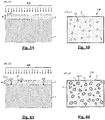
- the figures 3A and 3B are cross-sectional and top views with high magnification of part of the substrate 1 and of the etching mask 2 at an initial instant t1 of the phase P1. Since the reactive ion etching process is configured according to the method of the invention to be inhomogeneous and random, microscopic cavities 10 of random shapes, depths and distribution are seen to appear on the surface of the mask 2.
- the figures 4A and 4B are sectional and top views of the same part of the substrate and of the mask, at a final instant t2 of the phase P1. Certain cavities 10 have become orifices 11 passing through mask 2 while new cavities 10 have appeared.
- the assembly forms a random rough pattern 100 formed of cavities of random shapes, depths d1i, d1j, d1k and distribution.
- the nature and flow rate of the gases injected, the pressure in the enclosure, the RF power of the source and the bias power are closely related parameters whose respective values cause the inhomogeneity of the plasma and the etching. obtained.
- a key process parameter is the bias power applied to the substrate, ie the energy of the ions. Obtaining a roughness as shown on the Figures 4A, 4B requires acting on the bias power, by increasing this power until the desired result is obtained. It is therefore necessary to be able to control this parameter independently of the others, by choosing an appropriate reactor.
- a typical value range for bias powers is 10W-100W.
- the etching reactor used must therefore make it possible to independently control the energy of the ions (power of polarization) and the flow of ions (RF power of the source). It must also make it possible to regulate the temperature of the substrate, for example around 50° C. (this being generally obtained by the flow of a liquid between the substrate and the substrate holder), to operate at low pressure, for example a pressure less than 6.6661 Pa (50 mTorr), and to operate at high ion densities, for example greater than 10 10 cm -3 .
- the substrate etching phase P2 is initiated when the first orifices 11 appear in the etching mask 2.
- the phase P2 is preferably implemented with reactive ion etching parameters different from those of the phase P1, chosen so as to slowing the mask etching rate relative to the rate at which it would be etched if the etching parameters of the P1 phase were maintained, while maintaining the inhomogeneity of the etching process.
- phase 2 The moment when phase 2 is engaged can be detected by means of the gas analyzer 55 and the flowmeter, by detection of atoms of the material M1 of the substrate in the gas extracted from the reactor 50, here silicon atoms or derived compounds, for example silicon dioxide if the etching is done in the presence of oxygen.
- the end of phase P1 can be determined by timing, after calibration of the process.
- Phase P1 can also, in certain embodiments of the method of the invention, overlap phase P2, that is to say comprise a beginning of etching of the substrate which continues during phase P2 with parameters of different engraving.
- phases P1 and P2 can be combined and carried out without modifying the etching parameters, so that it is then not necessary to detect the end of phase P1.
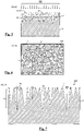
- the figure 5 is a sectional view of the aforementioned part of the substrate 1 and of the mask 2 at a time t3 occurring shortly after the start of the phase P2. Cavities 20 quickly appear in the substrate 1 by etching the latter through the holes 11 of the mask, while new cavities 10 appear in the mask 2 and others are transformed into holes 11, all with a speed etching less than that of substrate 1.
- the figure 6 is a top view of the aforementioned part of mask 2 at a later time t4 of phase P2.
- the cavities 10 created during phase 1 were mainly transformed into orifices 11 of larger opening, some of which joined to form orifices of even larger opening, through which cavities 20 were etched in the substrate, during that new cavities 10 have appeared in the mask and that others have turned into orifices 11.
- the figure 7 is a sectional view of the aforementioned part of the substrate 1 and of the mask 2 at a final or quasi-final instant t5 of the phase P2.
- the mask 2 only has a very small thickness, from one to a few atomic layers.
- the substrate 1 has a random rough pattern 200 comprising a plurality of cavities 20 of random shapes, depths and distribution.
- Phase P2 can be continued until complete disappearance of mask 2. Detection of the disappearance of the mask can be done by means of gas analyzer 55, when chemical species characteristic of material M2 are no longer detectable. Alternatively, phase P2 can be followed by a phase P3 for rinsing the substrate aimed at removing mask residues, for example rinsing with acetone when the material M2 is a resin.
- the P2 phase or if necessary the P3 phase, can be followed by a P4 phase of dopant implantation on the surface of the substrate, conventional in itself, making it possible to improve the absorption of the random rough surface in a domain wavelengths from 1200 nm to 1600 nm.
- the dopant can for example be sulfur, and be implanted for example with concentrations of the order of 10 14 to 10 16 atoms.cm ⁇ 2 .
- the etching of the substrate through the etching mask therefore has the effect of transferring the random rough pattern 100 of the mask to the substrate, to obtain the random rough pattern 200.
- the depths of the cavities 20 (or peak-valley heights) forming the rough pattern 200 denoted d2i, d2j, d2k... on the figure 7 , are a function of the initial depths of the cavities 10 formed in the mask 2 before the engagement of the phase P2, denoted d1i, d1j, dlk... on the figure 4A , with an amplification factor linked to the difference in etching speed of the substrate relative to that of the mask.
- the distribution of the depths of the cavities 20 of the pattern 200 obeys the same law of probability as the distribution of the depths of the cavities 10 of the pattern 100.
- the amplification factor of the depths of the cavities does not does not change their relative probability density.
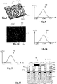
- the figure 8 shows an example of a rough pattern 100 obtained at the final instant t2 of phase P1 (appearance of the orifices 11 and start of etching of the substrate) and the figure 9 shows the probability density Pd(d1r) random depths d1r of the cavities 10 constituting this rough pattern.
- the figure 10 shows an aspect of the rough pattern 200 obtained at the end of phase P2, and the figure 11 shows the probability density Pd(d2r) of the random depths d2r of the cavities 20 of this rough pattern.
- the figures 9 and 11 show that the probability densities are identical and each take the form of a Gaussian function.
- the depths d1r of the cavities 10 are between about 0.1 micrometer and 1 micrometer. This last value is imposed here by the thickness E1 of the mask 2 and corresponds to the maximum depth of a cavity 10 which has become an orifice 11.
- the curve Pd(d1r) has a peak in the vicinity of 0.5 micrometer corresponding to the probability maximum depth of a cavity.
- the depths d2r of the cavities 20 are between approximately 0.5 micrometers and 5 micrometers.
- the curve Pd(d2r) has a peak in the vicinity of 2.5 micrometers corresponding to the maximum probability of depth of a cavity 20.
- the spatial distribution of the cavities itself obeys a law of probability
- the figure 12 shows by way of example the curve Pd(T2r) of the probability density of the random spatial period T2r of the array of cavities 20, considered here as the sum of a set of arrays of cavities of constant spatial period.
- the random spatial period T2r is between 0.1 micrometer and 3 micrometers and the Pd(T2r) function has a peak in the vicinity of a micrometer, corresponding to the highest probability of spatial period, therefore of distance between two cavities .
- the man of the art will note that the example of probability laws represented on the figures 9, 11 and 12 , here Gaussians, are purely exemplary and only reflect the experiments conducted. It is therefore not excluded that other probability laws may be obtained with variants of the method of the invention.
- such a random roughness pattern 200 has a broad absorption spectrum by combining the absorptions of each of the gratings which virtually constitute it, each grating having a maximum absorption at a wavelength different from that of the others.
- a rough pattern with the aforementioned structural features ( Fig. 9, 11, 12 ) and produced on a silicon substrate has excellent absorption of the order of 100% between 800 nm and 1000 nm, of 70 to 80% between 1000 nm and 1100 nm (infrared vision), and of the order of 20% beyond 1200 nm and up to 1600 nm, which can be improved by the P4 doping phase.
- the random texturing method according to the present invention is capable of various embodiments. It can be applied to various types of semiconductor substrates, doped or not, preferably monocrystalline, silicon, germanium, zinc sulphide (ZnS), Zinc selenide (ZnSe), and generally all monocrystals. Also, experiments could be conducted on multicrystalline substrates, to determine the applicability of the process to this type of substrate.
- the mask 2 can be in Chrome or in Aluminum. The mask is then deposited under vacuum with a thin layer technology, and can be very thin, for example 0.1 ⁇ m.
- Various types of photoresist can also be used, negative or positive.
- a positive resin mask has a typical thickness on the order of 0.5 micrometers to 2 micrometers while a negative resin mask can have a thickness of up to 8 micrometers.
- Embodiments of the method may also use a mask of silicon oxide (SiO2) or silicon nitride (Si3N4) typically 0.3 micrometers to 2 micrometers thick, formed by chemical vapor deposition.
- SiO2 silicon oxide
- Si3N4 silicon nitride
- M1 and M2 is within the reach of those skilled in the art, possibly after preliminary experiments making it possible to validate the choice envisaged.
- the reactive ion etching process can be implemented with various reactive gases, in particular fluorinated or chlorinated, such as carbon tetrafluoride (CF4) or sulfur hexafluoride (SF6), with or without oxygen, the present d oxygen resulting in the simultaneous passivation of the substrate if the latter is made of silicon.
- fluorinated or chlorinated such as carbon tetrafluoride (CF4) or sulfur hexafluoride (SF6)
- the random texturing method according to the present invention is also capable of various applications, in particular in the context of the manufacture of optoelectronic photoreceptor or photoemitter components requiring an antireflection photofunctional surface to optimize the collection or emission of photons, for example solar cells photovoltaics and image sensors.
- the figure 13 schematically represents a CMOS imager 60 produced according to a manufacturing method according to the invention including a random texturing step of the photofunctional surface of the imager. After implantation of photodiodes 61 and transistors 62 in the substrate 1 of the imager, as well as various interconnection elements not represented in a concern simplicity of the drawing, the surface 12 of the substrate 1 is subjected to a texturing process according to the invention.
- the latter After removal of the random etching mask and possible doping of the substrate, the latter is covered by a dielectric layer 63 receiving metal interconnection tracks 64 and a light mask 65, then by an RGB color filter 66 and microlenses 67 which focus incident light rays (L) on the photodiode regions 61.
Landscapes
- Drying Of Semiconductors (AREA)
- Light Receiving Elements (AREA)
Description
- La présente invention concerne un procédé de texturation aléatoire d'un substrat semi-conducteur.
- Il est connu que la texturation d'un substrat semi-conducteur, c'est-à-dire le fait de conférer au substrat une rugosité contrôlée, permet d'accroître son absorption optique dans le visible ou l'infrarouge. Les techniques de texturation trouvent ainsi diverses applications dans le domaine de la fabrication des composants optoélectroniques photorécepteurs ou photoémetteurs, notamment les imageurs et les cellules photovoltaïques, pour réaliser des surfaces photofonctionnelles (surfaces réceptrices ou émettrices) anti-réfléchissantes qui améliorent les performances de ces composants.
- La présente invention concerne plus particulièrement la texturation d'un substrat semi-conducteur par gravure ionique réactive, cette technique combinant gravure chimique et gravure physique à partir d'une même composition gazeuse ionisée.
- L'article "Silicon surface texturing by reactive ion etching" de H.F.W. Dekkers, F. Duerinckx, J. Szlufcik et J. NilS, OPTO-ELECTRONICS REVIEW 8(4), 311-3 16 (2000), décrit un procédé de texturation d'un substrat de silicium de type [111] consistant à soumettre le substrat au processus de gravure ionique réactive. Un tel procédé, souvent utilisé pour le traitement des cellules solaires, ne permet d'obtenir que des rugosités de faible amplitude, inférieure au micromètre, et une faible réduction de la réflectivité du matériau dans des longueurs d'ondes de l'ordre de 400-750 nm, soit dans le visible. De plus, le processus de gravure s'arrête spontanément lorsque la structure cristalline [111] s'est réorganisée à la surface du substrat.
- La présente invention vise l'obtention d'une plus forte rugosité, et plus particulièrement la réalisation de motifs rugueux d'une profondeur de l'ordre du micromètre à quelques micromètres, permettant d'améliorer l'absorption dans le proche infrarouge, et plus particulièrement dans le domaine des longueurs d'onde de 1000 à 1200 nm où se situe la majorité des applications d'imagerie nocturne, telles que la vidéo-surveillance infrarouge ou la vision de nuit.
- Il peut être démontré que le taux d'absorption offert par une surface rugueuse ordonnée et homogène, par exemple un réseau régulier de cavités sensiblement identiques, dépend de la profondeur des cavités qui le constituent et de leur période, et que la longueur d'onde à laquelle le réseau présente une absorption maximale dépend de la période de ces cavités. Par exemple, l'absorption d'un réseau de cavités identiques d'une période de l'ordre du micromètre et d'une profondeur également de l'ordre du micromètre est maximale au voisinage de la longueur d'onde 1000 nm.
- Pour obtenir une rugosité plus élevée que celle que permet la gravure directe d'un substrat, il est connu de faire appel à un masque de gravure.
- Par exemple, la demande
WO 2010/109692 décrit un procédé pour rendre un substrat rugueux comprenant des étapes de dépôt d'un masque dur sur le substrat, de réalisation d'ouvertures dans le masque au moyen d'un laser, de gravure humide isotrope du substrat au moyen d'une solution acide, à travers les ouvertures, pour former des cuvettes dans le substrat, puis de gravure humide anisotrope des cuvettes au moyen d'une solution alcaline, toujours à travers les ouvertures, pour l'obtention de cavités de forme pyramidale inversée. - Dans un même ordre d'idée, la demande de brevet
FR 2 981 196 - Ces divers procédés permettent certes de réaliser des cavités très profondes, mais présentent également l'inconvénient de ne permettre de réaliser que des structures régulières, ordonnées et homogènes.
- Or, il peut également être démontré qu'une surface de rugosité aléatoire présente, par rapport à une surface constituée de structures homogènes, l'avantage d'offrir une faible réflectivité sur une large gamme de longueurs d'ondes. Schématiquement, on peut en effet considérer qu'un motif de rugosité aléatoire est équivalent à la somme d'un ensemble de réseaux périodiques composés chacun de cavités présentant des profondeurs identiques, mais présentant entre eux des variations de profondeurs et de période spatiale obéissant à une loi de probabilité, par exemple une loi gaussienne. Un tel motif de rugosité aléatoire présente un large spectre d'absorption par combinaison des absorptions de chacun des réseaux qui le constituent virtuellement, chaque réseau présentant une absorption maximale à une longueur d'onde différente de celle des autres.
- Il pourrait ainsi être souhaité de prévoir un procédé permettant de fabriquer une surface rugueuse qui n'est pas "déterministe" (c'est-à-dire présentant un motif rugueux généré numériquement) et qui présente un motif rugueux aléatoire défini par une loi de probabilité.
- L'article "Statistically modified surfaces: experimental solutions for controlled scattered light" de V. Brissonneau, F. Flory, L. Escoubas, G. Berginc, J. Appl. Phys. 112, 114325 (2012), décrit un procédé permettant d'atteindre un tel objectif. Le procédé comprend une étape de formation, sur le substrat à texturer, d'une couche de résine photosensible comprenant un premier motif rugueux composé de cavités de formes, de profondeurs et de distributions aléatoires. Ce motif est obtenu par une étape de pré-insolation de la couche de résine, suivie d'une étape d'insolation aléatoire de celle-ci au moyen d'un faisceau de lumière laser, puis d'une étape de développement de la résine insolée. L'insolation aléatoire est mise en œuvre au moyen d'un modulateur spatial de lumière utilisant une matrice de micro-miroirs, associé à un élément de diffusion du faisceau laser. La distribution des profondeurs des cavités réalisées dans la résine, ou "hauteurs pics-vallées" ("peak-valley heights"), obéit à une loi de probabilité exponentielle et est comprise entre 0,4 et 1,6 micromètres.
- Le procédé comprend ensuite une étape de transfert du motif rugueux aléatoire sur le substrat, par gravure ionique réactive du substrat à travers la couche de résine. Le substrat étant plus rapidement gravé que la résine en raison de sa forte réactivité aux agents chimiques du gaz réactif, il se produit un phénomène "d'amplification" du relief du motif rugueux initial lors de son transfert, les profondeurs des cavités obtenues étant augmentées par un facteur de l'ordre de 2,5 dans les conditions expérimentales décrites par l'article. Par contre, cet accroissement du relief n'affecte pas la loi de distribution des profondeurs de cavités, qui reste inchangée, de sorte que la rugosité obtenue sur le semi-conducteur est elle-même aléatoire.
- Ce procédé présente toutefois l'inconvénient d'être complexe à mettre en œuvre, l'insolation d'une résine au moyen d'un modulateur spatial de lumière étant peu adaptée à une fabrication industrielle de composants dans l'industrie de la microélectronique.
- Ainsi, il pourrait être souhaité de prévoir un procédé de texturation aléatoire d'un substrat semi-conducteur ne nécessitant pas un modulateur spatial de lumière.
- A cet effet, la présente invention se fonde sur l'observation selon laquelle le processus de gravure ionique réactive est, par nature, un processus inhomogène à l'échelle microscopique. Un tel processus, s'il est contrôlé d'une manière appropriée telle que décrite plus loin, fait apparaître à la surface du matériau gravé des cavités microscopiques de profondeurs et de période aléatoires, équivalentes à la somme d'un ensemble de réseaux périodiques composés chacun de cavités présentant des profondeurs identiques et une période constante. La présente invention se fonde également sur l'observation, mise en évidence par le document précité, que le transfert sur un substrat d'un motif rugueux aléatoire réalisé sur une résine a pour effet d'accroître la profondeur du motif, sans altérer son caractère aléatoire. La présente invention se fonde ainsi sur l'idée "d'amplifier", par cette technique de transfert, un motif rugueux aléatoire obtenu en exploitant la propriété d'inhomogénéité de la gravure ionique réactive.
- Plus particulièrement, l'invention concerne un procédé de texturation aléatoire d'une surface photofonctionnelle d'un substrat semi-conducteur d'un composant photoémetteur ou photorécepteur, tel qu'exposé dans la revendication 1.
- Selon un mode de réalisation, le matériau du masque de gravure est choisi de manière à présenter une vitesse de gravure inférieure à la vitesse de gravure du substrat, avec des paramètres de gravure identiques, de manière que la profondeur aléatoire des cavités du second motif rugueux aléatoire soit statistiquement supérieure à la profondeur aléatoire des cavités du premier motif rugueux aléatoire.
- Selon un mode de réalisation, la vitesse de gravure du substrat est au moins 10 fois supérieure à la vitesse de gravure du masque.
- Selon un mode de réalisation, le masque de gravure comprend un matériau compris dans le groupe comprenant : les résines photosensibles, les métaux, un oxyde ou un nitrure de silicium.
- Selon un mode de réalisation, l'étape de transfert du premier motif rugueux aléatoire est poursuivie jusqu'à disparition du masque de gravure.
- Selon un mode de réalisation, l'étape de transfert du premier motif rugueux aléatoire est suivie d'une étape de retrait de résidus du masque de gravure.
- Selon un mode de réalisation, l'étape de formation de cavités dans le masque de gravure est réalisée avec des premiers paramètres de gravure ionique réactive, jusqu'à l'apparition d'orifices atteignant le substrat, et l'étape de transfert du premier motif rugueux aléatoire est essentiellement réalisée avec des seconds paramètres de gravure ionique réactive, choisis de manière à ralentir la vitesse de gravure du masque relativement à la vitesse avec laquelle le masque serait gravé si les premiers paramètres de gravure ionique réactive étaient maintenus.
- Selon un mode de réalisation, le commencement de l'étape de transfert du premier motif rugueux aléatoire dans le substrat est détecté par détection de la présence d'atomes du matériau du substrat dans un réacteur de gravure ionique réactive.
- Selon un mode de réalisation, les paramètres de gravure incluent au moins l'un des paramètres suivants : la pression d'un gaz réactif dans un réacteur de gravure, la tension appliquée à des électrodes d'ionisation du gaz réactif, et la composition du gaz réactif.
- Selon un mode de réalisation, le substrat est monocristallin.
- Des modes de réalisation de l'invention concernent également un procédé de fabrication d'un composant semi-conducteur photoémetteur ou photorécepteur, comprenant une étape de texturation aléatoire de la surface du substrat du composant selon le procédé de l'invention.
- Des modes de réalisation du procédé de l'invention seront décrits dans ce qui suit à titre non limitatif en se référant aux dessins annexés, parmi lesquels :
- la
figure 1 représente une étape préparatoire de dépôt d'un masque de gravure sur un substrat dont la surface doit être texturée aléatoirement, - la
figure 2 représente schématiquement un exemple de mise en œuvre, dans un réacteur de gravure ionique réactive, du procédé de texturation aléatoire selon l'invention, - les
figures 3A et 3B sont respectivement des vues en coupe et de dessus du substrat et du masque de gravure à un premier instant d'une première phase du procédé de texturation, - les
figures 4A et 4B sont respectivement des vues en coupe et de dessus du substrat et du masque de gravure à un second instant d'une première phase du procédé de texturation, - la
figure 5 est une vue en coupe du substrat et du masque de gravure à un premier instant d'une seconde phase du procédé de texturation, - la
figure 6 est une vue de dessus du substrat et du masque de gravure à un second instant de la seconde phase, - la
figure 7 est une vue en coupe du substrat et du masque de gravure à un troisième instant de la seconde phase, - la
figure 8 est une vue en perspective du masque de gravure au second instant de la première phase, - la
figure 9 montre un exemple de courbe de distribution des hauteurs pics-vallées d'un motif rugueux aléatoire présent sur le masque au second instant de la première phase, - la
figure 10 est une vue de dessus d'un exemple de substrat texturé aléatoirement selon le procédé de l'invention, - la
figure 11 montre une courbe de distribution des hauteurs pics-vallées d'un motif rugueux aléatoire présent à la surface du substrat de lafigure 10 , - la
figure 12 montre une courbe de distribution de la période spatiale aléatoire du motif rugueux aléatoire présent à la surface du substrat de lafigure 10 , et - la
figure 13 est une vue en coupe d'un composant optoélectronique réalisé selon un procédé de fabrication selon l'invention. - La
figure 1 représente schématiquement une étape préliminaire de dépôt d'un masque de gravure 2 sur un substrat 1 dont la surface doit être texturée aléatoirement au moyen du procédé selon l'invention. Le substrat 1 est en un matériau semi-conducteur M1 et le masque de gravure en un matériau M2. Le matériau M2 est de préférence choisi de manière à présenter une vitesse de gravure ionique réactive inférieure à la vitesse de gravure du matériau M1, avec des paramètres de gravure identiques. Dans un mode de réalisation du procédé, la vitesse de gravure du matériau M1 est au moins 10 fois supérieure à celle du matériau M2. - Le matériau M1 est par exemple du silicium monocristallin, et le matériau M2 est par exemple une résine photosensible positive déposée par centrifugation. Le masque de gravure 2 présente une épaisseur E1, par exemple 1 micromètre. Cette épaisseur, est, de préférence, la plus constante possible à l'échelle atomique, afin que des variations de cette épaisseur d'interfèrent pas avec le processus de gravure inhomogène du masque décrit plus loin.
- Le procédé de texturation aléatoire selon l'invention est mis en œuvre ici au moyen d'un réacteur 50 de gravure ionique réactive à électrodes parallèles, montré schématiquement sur la
figure 2 . Le réacteur 50 comporte une électrode inférieure 51 servant de support au substrat 1, une électrode supérieure 52, une entrée de gaz 53 ("inlet"), et une sortie de gaz 54 ("exhaust") reliée à une pompe à vide (non représentée) permettant de maintenir une très basse pression P dans le réacteur. Un analyseur de gaz 55, par exemple un spectromètre de masse, associé à un débitmètre, peut être prévu à la sortie du réacteur. L'électrode inférieure 51 est couplée capacitivement à un générateur 56 de tension alternative. Les parois du réacteur 50 et l'électrode supérieure 52 sont reliées à la masse du générateur 56. Le générateur 56 applique un champ électrique alternatif à l'électrode inférieure, oscillant par exemple à 13,56 Mhz, et fournit une puissance électrique ajustable, par exemple de l'ordre de la centaine de watts. - Le procédé de texturation aléatoire comprend deux phases:
- une phase P1 de gravure du masque de gravure 2 par gravure ionique réactive,
- une phase P2 de gravure du substrat 1 par l'intermédiaire du masque de gravure 2, également par gravure ionique réactive.
- Pour initier la phase P1, un gaz réactif 57 de composition C1, par exemple un gaz fluoré comme du tétrafluorure de carbone CF4, est injecté dans le réacteur 50. Un champ électrique oscillant, présent entre les électrodes 51, 52, ionise les molécules du gaz en leur arrachant des électrons, faisant apparaître un gaz ionisé (plasma) contenant des ions positifs (cations) et des électrons libres. Les électrons libres sont éjectés de la masse gazeuse tandis que les cations, plus lourds et moins réactifs aux variations du champ électrique, restent initialement en suspension entre les électrodes. Les électrons qui atteignent les parois du réacteur 50 ou l'électrode supérieure 52 sont évacués par la masse du générateur 56, tandis que ceux qui atteignent l'électrode inférieure 51 chargent celle-ci à un potentiel statique négatif. Lorsque la différence de potentiel statique entre les électrodes 51, 52 atteint un certain seuil, les ions attirés par l'électrode négative 51 sont fortement accélérés par le champ électrique et sont projetés à la surface du substrat 1, ici sur le masque 2.
- Ce processus de gravure est anisotrope et comporte deux composantes de processus qui agissent conjointement sur la surface bombardée par les ions :
- un processus de gravure chimique : les ions réagissent chimiquement avec la surface bombardée, généralement après avoir capturé des électrons libres au voisinage de la surface et avoir formé des radicaux,
- un processus de gravure physique (gravure plasma) lié à l'énergie cinétique des cations, qui arrachent des atomes de la surface bombardée par transfert d'énergie cinétique.
- Le processus de gravure chimique est généralement peu actif sur le masque, dont la gravure est essentiellement assurée par gravure physique. L'opérateur peut toutefois contrôler à tout moment la vitesse de gravure physique et la vitesse de gravure réactive en agissant sur des paramètres de gravure tels que la concentration du gaz, la tension inter-électrodes, ou la composition du gaz.
- Les
figures 3A et 3B sont des vues en coupe et de dessus avec un fort grossissement d'une partie du substrat 1 et du masque de gravure 2 à un instant initial t1 de la phase P1. Le processus de gravure ionique réactive étant configuré selon le procédé de l'invention pour être inhomogène et aléatoire, on voit apparaître à la surface du masque 2 des cavités microscopiques 10 de formes, profondeurs et distribution aléatoires. - Les
figures 4A et 4B sont des vues en coupe et de dessus de la même partie du substrat et du masque, à un instant final t2 de la phase P1. Certaines cavités 10 sont devenues des orifices 11 traversant le masque 2 tandis que de nouvelles cavités 10 sont apparues. L'ensemble forme un motif rugueux aléatoire 100 formé de cavités de formes, profondeurs d1i, d1j, d1k et distribution aléatoires. - Selon le procédé de l'invention, l'obtention de ce motif rugueux aléatoire formé de cavités de formes, profondeurs et distribution aléatoires, implique un contrôle du processus de gravure de manière qu'il soit parfaitement inhomogène. Cette inhomogénéité est notamment contrôlée par un ajustement des paramètres suivants :
- la température du substrat,
- le débit des gaz injectés,
- la pression dans l'enceinte du réacteur,
- le flux d'ions bombardant la surface à graver, également appelé densité d'ions, ou encore "puissance RF de la source",
- l'énergie de ces ions, ou "puissance de polarisation appliquée au substrat".
- De façon générale, la nature et le débit des gaz injectés, la pression dans l'enceinte, la puissance RF de la source et la puissance de polarisation sont des paramètres intimement liés dont les valeurs respectives provoquent l'inhomogénéité du plasma et de la gravure obtenue.
- Un paramètre clé du procédé est la puissance de polarisation appliquée au substrat, soit l'énergie des ions. L'obtention d'une rugosité telle que montrée sur les
figures 4A, 4B nécessite que l'on agisse sur la puissance de polarisation, en augmentant cette puissance jusqu'à obtention du résultat souhaité. Il faut donc pouvoir contrôler ce paramètre indépendamment des autres, par le choix d'un réacteur approprié. Une fourchette de valeurs typiques de puissances de polarisation est 10W-100W. - Le réacteur de gravure utilisé doit donc permettre de contrôler de façon indépendante l'énergie des ions (puissance de polarisation) et le flux d'ions (puissance RF de la source). Il doit permettre également de réguler la température du substrat, par exemple autour de 50°C (ceci étant généralement obtenu par écoulement d'un liquide entre le substrat et le porte-substrat), d'opérer à faible pression, par exemple une pression inférieure à 6.6661 Pa (50 mTorr), et d'opérer à des hautes densités d'ions, par exemple supérieures à 1010 cm-3.
- Il existe à cet effet deux catégories principales de réacteurs plasma dits "haute densité" pouvant être utilisés, qui diffèrent par la façon dont la puissance électrique est couplée au plasma : les réacteurs utilisant un couplage excitant des ondes progressives dit "ECR" ("Résonance Cyclotronique Electronique"), et les réacteurs à couplage inductif dits "ICP" ("Inductive Coupled Plasma"). Les réacteurs haute densité présentent l'intérêt, outre le fait d'opérer à basse pression (quelques dixièmes de Pa soit quelques mTorr), de contrôler indépendamment le flux et l'énergie des ions qui bombardent la région à graver. A cet effet, ces deux types de réacteurs utilisent deux générateurs RF:
- le premier permet la création du plasma via un couplage inductif (le plus souvent de type ICP) et donc le contrôle du flux ionique bombardant le substrat (puissance RF de la source),
- le second est couplé de manière capacitive au substrat et permet de contrôler l'énergie des ions bombardant ce dernier (puissance de polarisation). Ces deux types de générateurs RF utilisent des fréquences différentes, typiquement 12,56MHz pour le premier et 13,56MHz pour le second.
- La phase P2 de gravure du substrat est initiée lorsque les premiers orifices 11 apparaissent dans le masque de gravure 2. La phase P2 est de préférence mise en œuvre avec des paramètres de gravure ionique réactive différents de ceux de la phase P1, choisis de manière à ralentir la vitesse de gravure du masque relativement à la vitesse avec laquelle il serait gravé si les paramètres de gravure de la phase P1 étaient maintenus, tout en maintenant l'inhomogénéité du processus de gravure.
- L'instant où la phase 2 est engagée peut être détecté au moyen de l'analyseur de gaz 55 et du débitmètre, par détection d'atomes du matériau M1 du substrat dans le gaz extrait du réacteur 50, ici des atomes de silicium ou des composés dérivés, par exemple du dioxyde de silicium si la gravure est faite en présence d'oxygène. Alternativement, la fin de la phase P1 peut être déterminée par chronométrage, après étalonnage du procédé. La phase P1 peut également, dans certains modes de réalisation du procédé de l'invention, chevaucher la phase P2, c'est-à-dire comprendre un commencement de gravure du substrat qui se poursuit au cours de la phase P2 avec des paramètres de gravure différents. Également, dans d'autres modes de réalisation, les phases P1 et P2 peuvent être confondues et conduites sans modification des paramètres de gravure, de sorte qu'il n'est alors pas nécessaire de détecter la fin de la phase P1.
- La
figure 5 est une vue en coupe de la partie précitée du substrat 1 et du masque 2 à un instant t3 intervenant peu après le commencement de la phase P2. Des cavités 20 apparaissent rapidement dans le substrat 1 par gravure de celui-ci à travers les orifices 11 du masque, tandis que de nouvelles cavités 10 apparaissent dans le masque 2 et que d'autres se transforment en orifices 11, le tout avec une vitesse de gravure inférieure à celle du substrat 1. - La
figure 6 est une vue de dessus de la partie précitée du masque 2 à un instant ultérieur t4 de la phase P2. Les cavités 10 créées pendant la phase 1 ont été majoritairement transformées en orifices 11 de plus grande ouverture, dont certains se sont rejoints pour former des orifices d'encore plus grande ouverture, à travers lesquels des cavités 20 ont été gravées dans le substrat, pendant que de nouvelles cavités 10 sont apparues dans le masque et que d'autres se sont transformées en orifices 11. - La
figure 7 est une vue en coupe de la partie précitée du substrat 1 et du masque 2 à un instant t5 final ou quasi-final de la phase P2. Le masque 2 ne présente plus qu'une très faible épaisseur, d'une à quelques couches atomiques. Le substrat 1 présente un motif rugueux aléatoire 200 comportant une pluralité de cavités 20 de formes, profondeurs et distribution aléatoires. - La phase P2 peut être poursuivie jusqu'à disparition complète du masque 2. La détection de la disparition du masque peut être faite au moyen de l'analyseur de gaz 55, lorsque des espèces chimiques caractéristiques du matériau M2 ne sont plus détectables. Alternativement, la phase P2 peut être suivie d'une phase P3 de rinçage du substrat visant à retirer les résidus de masque, par exemple un rinçage à l'acétone quand le matériau M2 est une résine.
- La phase P2, ou le cas échéant la phase P3, peut être suivie d'une phase P4 d'implantation de dopant à la surface du substrat, en soi classique, permettant d'améliorer l'absorption de la surface rugueuse aléatoire dans un domaine de longueurs d'onde de 1200 nm à 1600 nm. Le dopant peut par exemple être du Soufre, et être implanté par exemple avec des concentrations de l'ordre de 1014 à 1016 atomes.cm-2.
- Comme cela a été indiqué plus haut, la gravure du substrat à travers le masque de gravure a donc pour effet de transférer sur le substrat le motif rugueux aléatoire 100 du masque, pour obtenir le motif rugueux aléatoire 200. Les profondeurs des cavités 20 (ou hauteurs pics-vallées) formant le motif rugueux 200, notées d2i, d2j, d2k... sur la
figure 7 , sont fonction des profondeurs initiales des cavités 10 formées dans le masque 2 avant l'engagement de la phase P2, notées d1i, d1j, dlk... sur lafigure 4A , avec un facteur d'amplification lié à la différence de vitesse de gravure du substrat relativement à celle du masque. - Il peut être démontré que la distribution des profondeurs des cavités 20 du motif 200 obéit à une même loi de probabilité que la distribution des profondeurs des cavités 10 du motif 100. En d'autres termes, le facteur d'amplification des profondeurs des cavités ne modifie pas leur densité de probabilité relative. Pour fixer les idées, la
figure 8 montre un exemple de motif rugueux 100 obtenu à l'instant final t2 de la phase P1 (apparition des orifices 11 et commencement de gravure du substrat) et lafigure 9 montre la densité de probabilité Pd(d1r) des profondeurs aléatoires d1r des cavités 10 constituant ce motif rugueux. Lafigure 10 montre un aspect du motif rugueux 200 obtenu au terme de la phase P2, et lafigure 11 montre la densité de probabilité Pd(d2r) des profondeurs aléatoires d2r des cavités 20 de ce motif rugueux. Lesfigures 9 et 11 montrent que les densités de probabilité sont identiques et prennent chacune la forme d'une fonction Gaussienne. Sur lafigure 9 , les profondeurs d1r des cavités 10 sont comprises entre environ 0,1 micromètre et 1 micromètre. Cette dernière valeur est imposée ici par l'épaisseur E1 du masque 2 et correspond à la profondeur maximale d'une cavité 10 devenue un orifice 11. La courbe Pd(d1r) présente un pic au voisinage de 0,5 micromètre correspondant à la probabilité maximale de profondeur d'une cavité. Sur lafigure 11 , les profondeurs d2r des cavités 20 sont comprises entre 0,5 micromètre environ et 5 micromètres. La courbe Pd(d2r) présente un pic au voisinage de 2,5 micromètres correspondant à la probabilité maximale de profondeur d'une cavité 20. L'homme de l'art notera que ces valeurs sont exemplatives et peuvent varier dans de larges proportions en fonction des matériaux M1, M2 utilisés et des paramètres de gravure retenus. - La distribution spatiale des cavités obéit elle-même à une loi de probabilité, et la
figure 12 montre à titre d'exemple la courbe Pd(T2r) de la densité de probabilité de la période spatiale aléatoire T2r du réseau de cavités 20, considéré ici comme la somme d'un ensemble de réseaux de cavités de période spatiale constante. Dans cet exemple, la période spatiale aléatoire T2r est comprise entre 0,1 micromètre et 3 micromètres et la fonction Pd(T2r) présente un pic au voisinage du micromètre, correspondant à la plus forte probabilité de période spatiale, donc de distance entre deux cavités. L'homme de l'art notera que l'exemple de lois de probabilité représentées sur lesfigures 9, 11 et 12 , ici des Gaussiennes, sont purement exemplatifs et reflètent seulement les expériences conduites. Il n'est donc pas exclu que d'autres lois de probabilité puissent être obtenues avec des variantes du procédé de l'invention. - Comme indiqué plus haut, un tel motif de rugosité aléatoire 200 présente un large spectre d'absorption par combinaison des absorptions de chacun des réseaux qui le constituent virtuellement, chaque réseau présentant une absorption maximale à une longueur d'onde différente de celle des autres. En particulier, un motif rugueux présentant les caractéristiques structurelles susmentionnées (
Fig. 9, 11, 12 ) et réalisé sur un substrat de silicium présente une excellente absorption de l'ordre de 100% entre 800 nm et 1000 nm, de 70 à 80% entre 1000 nm et 1100 nm (vision infrarouge), et de l'ordre de 20% au-delà de 1200 nm et jusqu'à 1600 nm, pouvant être améliorée par la phase de dopage P4. - Le procédé de texturation aléatoire selon la présente invention est susceptible de divers modes de réalisation. Il peut être appliqué à divers types de substrats semiconducteurs, dopés ou non, de préférence monocristallin, en silicium, germanium, sulfure de zinc (ZnS), Séléniure de Zinc (ZnSe), et de façon générale tous les monocristaux. Également, des expérimentations pourraient être conduites sur des substrats multi cristallins, pour déterminer l'applicabilité du procédé à ce type de substrat. Dans certains modes de réalisation, le masque 2 peut être en Chrome ou en Aluminium. Le masque est alors déposé sous vide avec une technologie pour couche mince, et peut être de très faible épaisseur, par exemple 0,1 µm. Divers types de résine photosensibles peuvent aussi être utilisées, négatives ou positives. Un masque en résine positive présente une épaisseur typique de l'ordre de 0,5 micromètre à 2 micromètres tandis qu'un masque en résine négative peut présenter une épaisseur jusqu'à 8 micromètres. Des modes de réalisation du procédé peuvent également utiliser un masque d'oxyde de silicium (SiO2) ou de nitrure de silicium (Si3N4) d'une épaisseur typique de 0,3 micromètre à 2 micromètres, formé par dépôt chimique en phase vapeur. De façon générale, le choix de diverses combinaisons de matériaux M1 et M2 est à la portée de l'homme de l'art, éventuellement après des expérimentations préalables permettant de valider le choix envisagé. Egalement, le processus de gravure ionique réactive peut être mis en œuvre avec divers gaz réactifs, notamment fluorés ou chlorés, comme du tétrafluorure de carbone (CF4) ou de l'hexafluorure de soufre (SF6), avec ou sans oxygène, la présente d'oxygène entraînant la passivation simultanée du substrat si celui-ci est en silicium.
- Le procédé de texturation aléatoire selon la présente invention est également susceptible de diverses applications, notamment dans le cadre de la fabrication de composants optoélectroniques photorécepteurs ou photoémetteurs nécessitant une surface photofonctionnelle antireflet pour optimiser la collecte ou l'émission de photons, par exemple les cellules solaires photovoltaïques et les capteurs d'image. A titre d'exemple, la
figure 13 représente schématiquement un imageur CMOS 60 réalisé selon un procédé de fabrication selon l'invention incluant une étape de texturation aléatoire de la surface photofonctionnelle de l'imageur. Après implantation de photodiodes 61 et de transistors 62 dans le substrat 1 de l'imageur, ainsi que divers éléments d'interconnexion non représentés dans un souci de simplicité du dessin, la surface 12 du substrat 1 est soumise à un procédé de texturation selon l'invention. Après retrait du masque de gravure aléatoire et dopage éventuel du substrat, ce dernier est recouvert par une couche diélectrique 63 recevant des pistes d'interconnexion 64 en métal et un masque de lumière 65, puis par un filtre de couleur RVB 66 et des microlentilles 67 qui focalisent des rayons lumineux incidents (L) sur les régions de photodiodes 61.
Claims (11)
- Procédé de texturation aléatoire d'une surface photofonctionnelle d'un substrat semi-conducteur (1) d'un composant photoémetteur ou photorécepteur (60), comprenant des étapes consistant à :- déposer un masque de gravure (2) sur le substrat (1),- former un premier motif rugueux aléatoire (100) dans le masque de gravure, ledit motif comprenant une pluralité de cavités (10, 11) de formes, profondeurs (dlr) et distribution aléatoires, ledit motif étant formé par gravure ionique réactive, dans un réacteur permettant un contrôle de l'énergie des ions assurant la gravure ionique réactive indépendamment du contrôle de la densité de ces ions,- transférer dans le substrat (1), par gravure ionique réactive du substrat, le premier motif rugueux aléatoire (100), pour obtenir à la surface du substrat un second motif rugueux aléatoire (200) composé de cavités (20) de formes, profondeurs (d2r) et distribution aléatoires, ce transfert continuant à graver le masque à une vitesse plus faible qu'au cours de la formation du motif rugueux,procédé comprenant une étape de réglage de l'énergie des ions consistant à augmenter l'énergie des ions jusqu'à l'obtention d'une gravure non homogène du masque de gravure et l'obtention de ladite pluralité de cavités (10, 11) de formes, profondeurs (dlr) et distribution aléatoires.
- Procédé selon la revendication 1, dans lequel le matériau (M2) du masque de gravure (2) est choisi de manière à présenter une vitesse de gravure inférieure à la vitesse de gravure du substrat, avec des paramètres de gravure identiques, de manière que la profondeur aléatoire (d2r) des cavités du second motif rugueux aléatoire (200) soit statistiquement supérieure à la profondeur aléatoire (d1r) des cavités du premier motif rugueux aléatoire.
- Procédé selon la revendication 2, dans lequel la vitesse de gravure du substrat (1) est au moins 10 fois supérieure à la vitesse de gravure du masque (2).
- Procédé selon l'une des revendications 1 à 3, dans lequel le masque de gravure comprend un matériau compris dans le groupe comprenant : les résines photosensibles, les métaux, un oxyde ou un nitrure de silicium.
- Procédé selon l'une des revendications 1 à 4, dans lequel l'étape de transfert du premier motif rugueux aléatoire est poursuivie jusqu'à disparition du masque de gravure.
- Procédé selon l'une des revendications 1 à 4, dans lequel l'étape de transfert du premier motif rugueux aléatoire est suivie d'une étape de retrait de résidus du masque de gravure.
- Procédé selon l'une des revendications 1 à 6, dans lequel- l'étape de formation de cavités (10, 11) dans le masque de gravure est réalisée avec des premiers paramètres de gravure ionique réactive, jusqu'à l'apparition d'orifices (11) atteignant le substrat, et- l'étape de transfert du premier motif rugueux aléatoire est essentiellement réalisée avec des seconds paramètres de gravure ionique réactive, choisis de manière à ralentir la vitesse de gravure du masque relativement à la vitesse avec laquelle le masque serait gravé si les premiers paramètres de gravure ionique réactive étaient maintenus.
- Procédé selon la revendication 7, dans lequel le commencement de l'étape de transfert du premier motif rugueux aléatoire dans le substrat est détecté par détection de la présence d'atomes du matériau (M1) du substrat dans un réacteur de gravure ionique réactive.
- Procédé selon la revendication 7, dans lequel les paramètres de gravure incluent au moins l'un des paramètres suivants : la pression d'un gaz réactif dans un réacteur de gravure, la tension appliquée à des électrodes d'ionisation du gaz réactif, et la composition du gaz réactif.
- Procédé selon l'une des revendications 1 à 9, dans lequel le substrat est monocristallin.
- Procédé de fabrication d'un composant semi-conducteur photoémetteur ou photorécepteur (60), comprenant une étape de texturation aléatoire de la surface du substrat du composant au moyen du procédé selon l'une des revendications 1 à 10.
Applications Claiming Priority (2)
| Application Number | Priority Date | Filing Date | Title |
|---|---|---|---|
| FR1455068A FR3022070B1 (fr) | 2014-06-04 | 2014-06-04 | Procede de texturation aleatoire d'un substrat semiconducteur |
| PCT/IB2015/054176 WO2015186064A1 (fr) | 2014-06-04 | 2015-06-02 | Procede de texturation aleatoire d'un substrat semi-conducteur |
Publications (2)
| Publication Number | Publication Date |
|---|---|
| EP3152786A1 EP3152786A1 (fr) | 2017-04-12 |
| EP3152786B1 true EP3152786B1 (fr) | 2022-05-04 |
Family
ID=51518966
Family Applications (1)
| Application Number | Title | Priority Date | Filing Date |
|---|---|---|---|
| EP15732422.9A Active EP3152786B1 (fr) | 2014-06-04 | 2015-06-02 | Procede de texturation aleatoire d'un substrat semi-conducteur |
Country Status (8)
| Country | Link |
|---|---|
| US (1) | US9941445B2 (fr) |
| EP (1) | EP3152786B1 (fr) |
| JP (1) | JP6617300B2 (fr) |
| KR (1) | KR102368258B1 (fr) |
| CA (1) | CA2953247C (fr) |
| FR (1) | FR3022070B1 (fr) |
| IL (1) | IL249360B (fr) |
| WO (1) | WO2015186064A1 (fr) |
Families Citing this family (7)
| Publication number | Priority date | Publication date | Assignee | Title |
|---|---|---|---|---|
| JPWO2018180765A1 (ja) | 2017-03-31 | 2020-02-13 | 日本電気株式会社 | テクスチャ構造の製造方法 |
| CN110622298B (zh) * | 2017-05-13 | 2023-09-22 | 应用材料公司 | 用于高质量间隙填充方案的循环可流动沉积和高密度等离子体处理处理 |
| KR101975795B1 (ko) * | 2017-12-20 | 2019-05-07 | 주식회사 한화 | 반구형 공진기 발란싱 장치 및 방법 |
| CN108365028A (zh) * | 2018-01-30 | 2018-08-03 | 北京世纪金光半导体有限公司 | 一种碳化硅器件表面制绒方法 |
| CN110137308B (zh) * | 2019-05-22 | 2021-03-26 | 中国科学院微电子研究所 | 一种红外吸收薄膜及其制备方法 |
| FR3116941A1 (fr) * | 2020-11-27 | 2022-06-03 | Commissariat A L'energie Atomique Et Aux Energies Alternatives | Procédé pour augmenter la rugosité de surface d’une couche métallique |
| US12094709B2 (en) | 2021-07-30 | 2024-09-17 | Applied Materials, Inc. | Plasma treatment process to densify oxide layers |
Citations (1)
| Publication number | Priority date | Publication date | Assignee | Title |
|---|---|---|---|---|
| WO2015043606A1 (fr) * | 2013-09-27 | 2015-04-02 | Danmarks Tekniske Universitet | Cellules solaires à base de silicium nanostructuré et procédés de production de ces cellules solaires |
Family Cites Families (29)
| Publication number | Priority date | Publication date | Assignee | Title |
|---|---|---|---|---|
| JPS5723226A (en) * | 1980-07-17 | 1982-02-06 | Nippon Telegr & Teleph Corp <Ntt> | Plasma etching device |
| JPS58140125A (ja) * | 1982-02-16 | 1983-08-19 | Matsushita Electric Ind Co Ltd | ドライエツチング方法 |
| JPH01101634A (ja) * | 1987-10-15 | 1989-04-19 | Oki Electric Ind Co Ltd | パターン形成方法 |
| JP2888258B2 (ja) * | 1990-11-30 | 1999-05-10 | 東京エレクトロン株式会社 | 基板処理装置および基板処理方法 |
| JPH05234959A (ja) * | 1991-08-16 | 1993-09-10 | Hitachi Ltd | ドライエッチング方法及びドライエッチング装置 |
| JPH06275562A (ja) * | 1993-03-24 | 1994-09-30 | Toshiba Emi Ltd | プラズマ処理装置 |
| JPH08306666A (ja) * | 1995-05-02 | 1996-11-22 | Sony Corp | ドライエッチング装置 |
| JPH1098021A (ja) * | 1996-09-19 | 1998-04-14 | Seiko Epson Corp | 半導体装置の製造方法 |
| JPH10150046A (ja) * | 1996-11-15 | 1998-06-02 | Texas Instr Japan Ltd | 半導体装置及びその製造方法 |
| JPH10223990A (ja) * | 1997-02-12 | 1998-08-21 | Hitachi Ltd | 半導体光素子の製造方法およびそれを用いた半導体光素子ならびにそれを用いた光応用システム |
| JP4167328B2 (ja) * | 1997-08-04 | 2008-10-15 | 東芝松下ディスプレイテクノロジー株式会社 | 薄膜のドライエッチング方法および薄膜半導体装置の製造方法 |
| JP2000012519A (ja) * | 1998-06-17 | 2000-01-14 | Toshiba Corp | 半導体装置の製造方法 |
| JP4258789B2 (ja) * | 1999-03-17 | 2009-04-30 | 東京エレクトロン株式会社 | ガス処理方法 |
| JP3466144B2 (ja) * | 2000-09-22 | 2003-11-10 | 士郎 酒井 | 半導体の表面を荒くする方法 |
| JP4077312B2 (ja) * | 2001-12-28 | 2008-04-16 | 株式会社東芝 | 発光素子の製造方法および発光素子 |
| US7901952B2 (en) * | 2003-05-16 | 2011-03-08 | Applied Materials, Inc. | Plasma reactor control by translating desired values of M plasma parameters to values of N chamber parameters |
| US7247218B2 (en) * | 2003-05-16 | 2007-07-24 | Applied Materials, Inc. | Plasma density, energy and etch rate measurements at bias power input and real time feedback control of plasma source and bias power |
| JP2005050917A (ja) * | 2003-07-30 | 2005-02-24 | Toshiba Corp | 半導体装置及びその製造方法 |
| KR101424824B1 (ko) * | 2005-11-18 | 2014-08-01 | 레플리서러스 그룹 에스에이에스 | 다중 층 구조 형성 방법 |
| JP2008072032A (ja) * | 2006-09-15 | 2008-03-27 | Toshiba Corp | 半導体装置の製造方法 |
| KR101283261B1 (ko) * | 2007-05-21 | 2013-07-11 | 엘지이노텍 주식회사 | 발광 소자 및 그 제조방법 |
| JP2009277979A (ja) * | 2008-05-16 | 2009-11-26 | Mitsubishi Electric Corp | 基板の粗面化方法、光起電力装置およびその製造方法 |
| JP5276926B2 (ja) * | 2008-08-25 | 2013-08-28 | ラピスセミコンダクタ株式会社 | コンタクトホール側壁の抵抗値測定方法 |
| US8652869B2 (en) | 2009-03-25 | 2014-02-18 | Mitsubishi Electric Corporation | Method for roughening substrate surface and method for manufacturing photovoltaic device |
| KR101250450B1 (ko) * | 2010-07-30 | 2013-04-08 | 광주과학기술원 | 마이크로 나노 조합구조의 제조방법 및 마이크로 나노 조합구조가 집적된 광소자의 제조방법 |
| CN103237745B (zh) * | 2010-11-01 | 2016-05-04 | 因特瓦克公司 | 在硅晶片上形成表面纹理的干法蚀刻方法 |
| US9956743B2 (en) * | 2010-12-20 | 2018-05-01 | The Regents Of The University Of California | Superhydrophobic and superoleophobic nanosurfaces |
| FR2981196B1 (fr) | 2011-10-06 | 2014-12-26 | Altis Semiconductor Snc | Procede de fabrication d'un substrat semi-conducteur structure |
| KR101942092B1 (ko) * | 2012-07-30 | 2019-01-25 | 한국전자통신연구원 | 유기발광소자 제조방법 |
-
2014
- 2014-06-04 FR FR1455068A patent/FR3022070B1/fr active Active
-
2015
- 2015-06-02 CA CA2953247A patent/CA2953247C/fr active Active
- 2015-06-02 JP JP2016571237A patent/JP6617300B2/ja active Active
- 2015-06-02 KR KR1020177000252A patent/KR102368258B1/ko active Active
- 2015-06-02 US US15/316,387 patent/US9941445B2/en active Active
- 2015-06-02 EP EP15732422.9A patent/EP3152786B1/fr active Active
- 2015-06-02 WO PCT/IB2015/054176 patent/WO2015186064A1/fr not_active Ceased
-
2016
- 2016-12-04 IL IL249360A patent/IL249360B/en unknown
Patent Citations (2)
| Publication number | Priority date | Publication date | Assignee | Title |
|---|---|---|---|---|
| WO2015043606A1 (fr) * | 2013-09-27 | 2015-04-02 | Danmarks Tekniske Universitet | Cellules solaires à base de silicium nanostructuré et procédés de production de ces cellules solaires |
| EP3050120A1 (fr) * | 2013-09-27 | 2016-08-03 | Danmarks Tekniske Universitet | Cellules solaires à base de silicium nanostructuré et procédés de production de ces cellules solaires |
Also Published As
| Publication number | Publication date |
|---|---|
| IL249360A0 (en) | 2017-02-28 |
| US9941445B2 (en) | 2018-04-10 |
| KR20170016932A (ko) | 2017-02-14 |
| CA2953247C (fr) | 2023-09-19 |
| JP6617300B2 (ja) | 2019-12-11 |
| FR3022070B1 (fr) | 2016-06-24 |
| CA2953247A1 (fr) | 2015-12-10 |
| KR102368258B1 (ko) | 2022-02-28 |
| EP3152786A1 (fr) | 2017-04-12 |
| IL249360B (en) | 2021-07-29 |
| JP2017518646A (ja) | 2017-07-06 |
| US20170141264A1 (en) | 2017-05-18 |
| WO2015186064A1 (fr) | 2015-12-10 |
| FR3022070A1 (fr) | 2015-12-11 |
Similar Documents
| Publication | Publication Date | Title |
|---|---|---|
| CA2953247C (fr) | Procede de texturation aleatoire d'un substrat semi-conducteur | |
| EP2939262B1 (fr) | Procédé microélectronique de gravure d'une couche | |
| EP2471103B1 (fr) | Procédé de texturation de la surface d'un substrat de silicium et substrat de silicium texturé pour cellule solaire | |
| FR3013503A1 (fr) | Procede de gravure selective d’un masque dispose sur un substrat silicie | |
| EP3238233B1 (fr) | Procédé de réalisation de motifs | |
| JP2017518646A5 (fr) | ||
| EP2784803A2 (fr) | Procédé de gravure autolimitant à niveaux multiples | |
| EP3249468B1 (fr) | Procédé de réalisation de motifs | |
| BE1025681B1 (fr) | Procédé de traitement d'un substrat et dispositif de circuit intégré | |
| EP3465739B1 (fr) | Procédé de formation d'un motif de guidage fonctionnalisé pour un procédé de grapho-épitaxie | |
| EP3631843B1 (fr) | Procédé de réalisation de motifs dans un substrat | |
| EP3252830B1 (fr) | Procédé de réalisation de motifs par implantations ioniques | |
| EP2160808A1 (fr) | Procede de fabrication de dispositifs de lumiere optimise par l'utilisation de materiaux artificiels | |
| EP2579321B1 (fr) | Procédé de fabrication d'un substrat semi-conducteur structuré | |
| EP3358631B1 (fr) | Formation de reliefs à la surface d'un substrat | |
| EP1735843A1 (fr) | Procede de fabrication de plaques de silicium polycristallin | |
| EP3840019B1 (fr) | Procédé de formation d'une portion poreuse dans un substrat | |
| EP2795677A1 (fr) | Procede de texturation de la surface d'un substrat de silicium, substrat structure et dispositif photovoltaïque comportant un tel substrat structure | |
| WO2000068981A1 (fr) | Procede de croissance d'une couche d'oxyde de silicium de faible epaisseur sur une surface de substrat de silicium et machine a deux reacteurs |
Legal Events
| Date | Code | Title | Description |
|---|---|---|---|
| STAA | Information on the status of an ep patent application or granted ep patent |
Free format text: STATUS: THE INTERNATIONAL PUBLICATION HAS BEEN MADE |
|
| PUAI | Public reference made under article 153(3) epc to a published international application that has entered the european phase |
Free format text: ORIGINAL CODE: 0009012 |
|
| STAA | Information on the status of an ep patent application or granted ep patent |
Free format text: STATUS: REQUEST FOR EXAMINATION WAS MADE |
|
| 17P | Request for examination filed |
Effective date: 20161201 |
|
| AK | Designated contracting states |
Kind code of ref document: A1 Designated state(s): AL AT BE BG CH CY CZ DE DK EE ES FI FR GB GR HR HU IE IS IT LI LT LU LV MC MK MT NL NO PL PT RO RS SE SI SK SM TR |
|
| AX | Request for extension of the european patent |
Extension state: BA ME |
|
| DAV | Request for validation of the european patent (deleted) | ||
| DAX | Request for extension of the european patent (deleted) | ||
| STAA | Information on the status of an ep patent application or granted ep patent |
Free format text: STATUS: EXAMINATION IS IN PROGRESS |
|
| 17Q | First examination report despatched |
Effective date: 20200218 |
|
| GRAP | Despatch of communication of intention to grant a patent |
Free format text: ORIGINAL CODE: EPIDOSNIGR1 |
|
| STAA | Information on the status of an ep patent application or granted ep patent |
Free format text: STATUS: GRANT OF PATENT IS INTENDED |
|
| INTG | Intention to grant announced |
Effective date: 20211209 |
|
| GRAS | Grant fee paid |
Free format text: ORIGINAL CODE: EPIDOSNIGR3 |
|
| GRAA | (expected) grant |
Free format text: ORIGINAL CODE: 0009210 |
|
| STAA | Information on the status of an ep patent application or granted ep patent |
Free format text: STATUS: THE PATENT HAS BEEN GRANTED |
|
| AK | Designated contracting states |
Kind code of ref document: B1 Designated state(s): AL AT BE BG CH CY CZ DE DK EE ES FI FR GB GR HR HU IE IS IT LI LT LU LV MC MK MT NL NO PL PT RO RS SE SI SK SM TR |
|
| REG | Reference to a national code |
Ref country code: GB Ref legal event code: FG4D Free format text: NOT ENGLISH |
|
| REG | Reference to a national code |
Ref country code: CH Ref legal event code: EP |
|
| REG | Reference to a national code |
Ref country code: AT Ref legal event code: REF Ref document number: 1490052 Country of ref document: AT Kind code of ref document: T Effective date: 20220515 |
|
| REG | Reference to a national code |
Ref country code: DE Ref legal event code: R096 Ref document number: 602015078678 Country of ref document: DE |
|
| REG | Reference to a national code |
Ref country code: IE Ref legal event code: FG4D Free format text: LANGUAGE OF EP DOCUMENT: FRENCH |
|
| REG | Reference to a national code |
Ref country code: FI Ref legal event code: FGE |
|
| REG | Reference to a national code |
Ref country code: NL Ref legal event code: FP |
|
| REG | Reference to a national code |
Ref country code: LT Ref legal event code: MG9D |
|
| REG | Reference to a national code |
Ref country code: AT Ref legal event code: MK05 Ref document number: 1490052 Country of ref document: AT Kind code of ref document: T Effective date: 20220504 |
|
| PG25 | Lapsed in a contracting state [announced via postgrant information from national office to epo] |
Ref country code: SE Free format text: LAPSE BECAUSE OF FAILURE TO SUBMIT A TRANSLATION OF THE DESCRIPTION OR TO PAY THE FEE WITHIN THE PRESCRIBED TIME-LIMIT Effective date: 20220504 Ref country code: PT Free format text: LAPSE BECAUSE OF FAILURE TO SUBMIT A TRANSLATION OF THE DESCRIPTION OR TO PAY THE FEE WITHIN THE PRESCRIBED TIME-LIMIT Effective date: 20220905 Ref country code: NO Free format text: LAPSE BECAUSE OF FAILURE TO SUBMIT A TRANSLATION OF THE DESCRIPTION OR TO PAY THE FEE WITHIN THE PRESCRIBED TIME-LIMIT Effective date: 20220804 Ref country code: LT Free format text: LAPSE BECAUSE OF FAILURE TO SUBMIT A TRANSLATION OF THE DESCRIPTION OR TO PAY THE FEE WITHIN THE PRESCRIBED TIME-LIMIT Effective date: 20220504 Ref country code: HR Free format text: LAPSE BECAUSE OF FAILURE TO SUBMIT A TRANSLATION OF THE DESCRIPTION OR TO PAY THE FEE WITHIN THE PRESCRIBED TIME-LIMIT Effective date: 20220504 Ref country code: ES Free format text: LAPSE BECAUSE OF FAILURE TO SUBMIT A TRANSLATION OF THE DESCRIPTION OR TO PAY THE FEE WITHIN THE PRESCRIBED TIME-LIMIT Effective date: 20220504 Ref country code: BG Free format text: LAPSE BECAUSE OF FAILURE TO SUBMIT A TRANSLATION OF THE DESCRIPTION OR TO PAY THE FEE WITHIN THE PRESCRIBED TIME-LIMIT Effective date: 20220804 Ref country code: AT Free format text: LAPSE BECAUSE OF FAILURE TO SUBMIT A TRANSLATION OF THE DESCRIPTION OR TO PAY THE FEE WITHIN THE PRESCRIBED TIME-LIMIT Effective date: 20220504 |
|
| PG25 | Lapsed in a contracting state [announced via postgrant information from national office to epo] |
Ref country code: RS Free format text: LAPSE BECAUSE OF FAILURE TO SUBMIT A TRANSLATION OF THE DESCRIPTION OR TO PAY THE FEE WITHIN THE PRESCRIBED TIME-LIMIT Effective date: 20220504 Ref country code: PL Free format text: LAPSE BECAUSE OF FAILURE TO SUBMIT A TRANSLATION OF THE DESCRIPTION OR TO PAY THE FEE WITHIN THE PRESCRIBED TIME-LIMIT Effective date: 20220504 Ref country code: LV Free format text: LAPSE BECAUSE OF FAILURE TO SUBMIT A TRANSLATION OF THE DESCRIPTION OR TO PAY THE FEE WITHIN THE PRESCRIBED TIME-LIMIT Effective date: 20220504 Ref country code: IS Free format text: LAPSE BECAUSE OF FAILURE TO SUBMIT A TRANSLATION OF THE DESCRIPTION OR TO PAY THE FEE WITHIN THE PRESCRIBED TIME-LIMIT Effective date: 20220904 |
|
| PG25 | Lapsed in a contracting state [announced via postgrant information from national office to epo] |
Ref country code: SM Free format text: LAPSE BECAUSE OF FAILURE TO SUBMIT A TRANSLATION OF THE DESCRIPTION OR TO PAY THE FEE WITHIN THE PRESCRIBED TIME-LIMIT Effective date: 20220504 Ref country code: SK Free format text: LAPSE BECAUSE OF FAILURE TO SUBMIT A TRANSLATION OF THE DESCRIPTION OR TO PAY THE FEE WITHIN THE PRESCRIBED TIME-LIMIT Effective date: 20220504 Ref country code: RO Free format text: LAPSE BECAUSE OF FAILURE TO SUBMIT A TRANSLATION OF THE DESCRIPTION OR TO PAY THE FEE WITHIN THE PRESCRIBED TIME-LIMIT Effective date: 20220504 Ref country code: EE Free format text: LAPSE BECAUSE OF FAILURE TO SUBMIT A TRANSLATION OF THE DESCRIPTION OR TO PAY THE FEE WITHIN THE PRESCRIBED TIME-LIMIT Effective date: 20220504 Ref country code: DK Free format text: LAPSE BECAUSE OF FAILURE TO SUBMIT A TRANSLATION OF THE DESCRIPTION OR TO PAY THE FEE WITHIN THE PRESCRIBED TIME-LIMIT Effective date: 20220504 Ref country code: CZ Free format text: LAPSE BECAUSE OF FAILURE TO SUBMIT A TRANSLATION OF THE DESCRIPTION OR TO PAY THE FEE WITHIN THE PRESCRIBED TIME-LIMIT Effective date: 20220504 |
|
| REG | Reference to a national code |
Ref country code: CH Ref legal event code: PL |
|
| REG | Reference to a national code |
Ref country code: DE Ref legal event code: R097 Ref document number: 602015078678 Country of ref document: DE |
|
| PG25 | Lapsed in a contracting state [announced via postgrant information from national office to epo] |
Ref country code: MC Free format text: LAPSE BECAUSE OF FAILURE TO SUBMIT A TRANSLATION OF THE DESCRIPTION OR TO PAY THE FEE WITHIN THE PRESCRIBED TIME-LIMIT Effective date: 20220504 |
|
| PLBE | No opposition filed within time limit |
Free format text: ORIGINAL CODE: 0009261 |
|
| STAA | Information on the status of an ep patent application or granted ep patent |
Free format text: STATUS: NO OPPOSITION FILED WITHIN TIME LIMIT |
|
| PG25 | Lapsed in a contracting state [announced via postgrant information from national office to epo] |
Ref country code: AL Free format text: LAPSE BECAUSE OF FAILURE TO SUBMIT A TRANSLATION OF THE DESCRIPTION OR TO PAY THE FEE WITHIN THE PRESCRIBED TIME-LIMIT Effective date: 20220504 |
|
| 26N | No opposition filed |
Effective date: 20230207 |
|
| PG25 | Lapsed in a contracting state [announced via postgrant information from national office to epo] |
Ref country code: LU Free format text: LAPSE BECAUSE OF NON-PAYMENT OF DUE FEES Effective date: 20220602 Ref country code: LI Free format text: LAPSE BECAUSE OF NON-PAYMENT OF DUE FEES Effective date: 20220630 Ref country code: IE Free format text: LAPSE BECAUSE OF NON-PAYMENT OF DUE FEES Effective date: 20220602 Ref country code: CH Free format text: LAPSE BECAUSE OF NON-PAYMENT OF DUE FEES Effective date: 20220630 |
|
| PG25 | Lapsed in a contracting state [announced via postgrant information from national office to epo] |
Ref country code: SI Free format text: LAPSE BECAUSE OF FAILURE TO SUBMIT A TRANSLATION OF THE DESCRIPTION OR TO PAY THE FEE WITHIN THE PRESCRIBED TIME-LIMIT Effective date: 20220504 |
|
| P01 | Opt-out of the competence of the unified patent court (upc) registered |
Effective date: 20230601 |
|
| PG25 | Lapsed in a contracting state [announced via postgrant information from national office to epo] |
Ref country code: HU Free format text: LAPSE BECAUSE OF FAILURE TO SUBMIT A TRANSLATION OF THE DESCRIPTION OR TO PAY THE FEE WITHIN THE PRESCRIBED TIME-LIMIT; INVALID AB INITIO Effective date: 20150602 |
|
| PG25 | Lapsed in a contracting state [announced via postgrant information from national office to epo] |
Ref country code: MK Free format text: LAPSE BECAUSE OF FAILURE TO SUBMIT A TRANSLATION OF THE DESCRIPTION OR TO PAY THE FEE WITHIN THE PRESCRIBED TIME-LIMIT Effective date: 20220504 Ref country code: CY Free format text: LAPSE BECAUSE OF FAILURE TO SUBMIT A TRANSLATION OF THE DESCRIPTION OR TO PAY THE FEE WITHIN THE PRESCRIBED TIME-LIMIT Effective date: 20220504 |
|
| PG25 | Lapsed in a contracting state [announced via postgrant information from national office to epo] |
Ref country code: TR Free format text: LAPSE BECAUSE OF FAILURE TO SUBMIT A TRANSLATION OF THE DESCRIPTION OR TO PAY THE FEE WITHIN THE PRESCRIBED TIME-LIMIT Effective date: 20220504 |
|
| PG25 | Lapsed in a contracting state [announced via postgrant information from national office to epo] |
Ref country code: MT Free format text: LAPSE BECAUSE OF FAILURE TO SUBMIT A TRANSLATION OF THE DESCRIPTION OR TO PAY THE FEE WITHIN THE PRESCRIBED TIME-LIMIT Effective date: 20220504 |
|
| PG25 | Lapsed in a contracting state [announced via postgrant information from national office to epo] |
Ref country code: BG Free format text: LAPSE BECAUSE OF FAILURE TO SUBMIT A TRANSLATION OF THE DESCRIPTION OR TO PAY THE FEE WITHIN THE PRESCRIBED TIME-LIMIT Effective date: 20220504 |
|
| REG | Reference to a national code |
Ref country code: DE Ref legal event code: R079 Ref document number: 602015078678 Country of ref document: DE Free format text: PREVIOUS MAIN CLASS: H01L0031023600 Ipc: H10F0077700000 |
|
| PG25 | Lapsed in a contracting state [announced via postgrant information from national office to epo] |
Ref country code: BG Free format text: LAPSE BECAUSE OF FAILURE TO SUBMIT A TRANSLATION OF THE DESCRIPTION OR TO PAY THE FEE WITHIN THE PRESCRIBED TIME-LIMIT Effective date: 20220504 |
|
| PG25 | Lapsed in a contracting state [announced via postgrant information from national office to epo] |
Ref country code: GR Free format text: LAPSE BECAUSE OF NON-PAYMENT OF DUE FEES Effective date: 20220504 |
|
| PG25 | Lapsed in a contracting state [announced via postgrant information from national office to epo] |
Ref country code: GR Free format text: LAPSE BECAUSE OF NON-PAYMENT OF DUE FEES Effective date: 20220504 |
|
| PGFP | Annual fee paid to national office [announced via postgrant information from national office to epo] |
Ref country code: FI Payment date: 20250626 Year of fee payment: 11 |
|
| PGFP | Annual fee paid to national office [announced via postgrant information from national office to epo] |
Ref country code: GB Payment date: 20250626 Year of fee payment: 11 |
|
| PGFP | Annual fee paid to national office [announced via postgrant information from national office to epo] |
Ref country code: NL Payment date: 20250627 Year of fee payment: 11 Ref country code: BE Payment date: 20250630 Year of fee payment: 11 |
|
| PGFP | Annual fee paid to national office [announced via postgrant information from national office to epo] |
Ref country code: FR Payment date: 20250617 Year of fee payment: 11 |
|
| PGFP | Annual fee paid to national office [announced via postgrant information from national office to epo] |
Ref country code: DE Payment date: 20250725 Year of fee payment: 11 |
|
| PGFP | Annual fee paid to national office [announced via postgrant information from national office to epo] |
Ref country code: IT Payment date: 20250626 Year of fee payment: 11 |