EP3140848B1 - Appareil et procédé d'inspection d'échantillon à l'aide d'une pluralité de faisceaux de particules chargées - Google Patents
Appareil et procédé d'inspection d'échantillon à l'aide d'une pluralité de faisceaux de particules chargées Download PDFInfo
- Publication number
- EP3140848B1 EP3140848B1 EP15726384.9A EP15726384A EP3140848B1 EP 3140848 B1 EP3140848 B1 EP 3140848B1 EP 15726384 A EP15726384 A EP 15726384A EP 3140848 B1 EP3140848 B1 EP 3140848B1
- Authority
- EP
- European Patent Office
- Prior art keywords
- sample
- charged particle
- particle beams
- primary charged
- array
- Prior art date
- Legal status (The legal status is an assumption and is not a legal conclusion. Google has not performed a legal analysis and makes no representation as to the accuracy of the status listed.)
- Active
Links
- 239000002245 particle Substances 0.000 title claims description 135
- 238000000034 method Methods 0.000 title claims description 10
- 239000000463 material Substances 0.000 claims description 51
- 230000003287 optical effect Effects 0.000 claims description 20
- 230000005540 biological transmission Effects 0.000 claims description 11
- 238000003384 imaging method Methods 0.000 claims description 4
- 238000010894 electron beam technology Methods 0.000 description 20
- 238000001514 detection method Methods 0.000 description 8
- 230000003993 interaction Effects 0.000 description 8
- 239000000470 constituent Substances 0.000 description 5
- 238000005136 cathodoluminescence Methods 0.000 description 4
- 229910019655 synthetic inorganic crystalline material Inorganic materials 0.000 description 4
- 230000000694 effects Effects 0.000 description 2
- 230000005284 excitation Effects 0.000 description 2
- 229910052751 metal Inorganic materials 0.000 description 2
- 239000002184 metal Substances 0.000 description 2
- 230000011218 segmentation Effects 0.000 description 2
- OKTJSMMVPCPJKN-UHFFFAOYSA-N Carbon Chemical compound [C] OKTJSMMVPCPJKN-UHFFFAOYSA-N 0.000 description 1
- 206010010071 Coma Diseases 0.000 description 1
- 238000010521 absorption reaction Methods 0.000 description 1
- 239000004411 aluminium Substances 0.000 description 1
- 229910052782 aluminium Inorganic materials 0.000 description 1
- XAGFODPZIPBFFR-UHFFFAOYSA-N aluminium Chemical compound [Al] XAGFODPZIPBFFR-UHFFFAOYSA-N 0.000 description 1
- 239000013078 crystal Substances 0.000 description 1
- 230000001419 dependent effect Effects 0.000 description 1
- 239000002223 garnet Substances 0.000 description 1
- 229910000204 garnet group Inorganic materials 0.000 description 1
- 229910021389 graphene Inorganic materials 0.000 description 1
- 150000002500 ions Chemical class 0.000 description 1
- 230000007246 mechanism Effects 0.000 description 1
- 238000000926 separation method Methods 0.000 description 1
- 238000004611 spectroscopical analysis Methods 0.000 description 1
- 229910052727 yttrium Inorganic materials 0.000 description 1
- 229910019901 yttrium aluminum garnet Inorganic materials 0.000 description 1
- VWQVUPCCIRVNHF-UHFFFAOYSA-N yttrium atom Chemical compound [Y] VWQVUPCCIRVNHF-UHFFFAOYSA-N 0.000 description 1
Images


Classifications
-
- H—ELECTRICITY
- H01—ELECTRIC ELEMENTS
- H01J—ELECTRIC DISCHARGE TUBES OR DISCHARGE LAMPS
- H01J37/00—Discharge tubes with provision for introducing objects or material to be exposed to the discharge, e.g. for the purpose of examination or processing thereof
- H01J37/02—Details
- H01J37/244—Detectors; Associated components or circuits therefor
-
- H—ELECTRICITY
- H01—ELECTRIC ELEMENTS
- H01J—ELECTRIC DISCHARGE TUBES OR DISCHARGE LAMPS
- H01J37/00—Discharge tubes with provision for introducing objects or material to be exposed to the discharge, e.g. for the purpose of examination or processing thereof
- H01J37/02—Details
- H01J37/04—Arrangements of electrodes and associated parts for generating or controlling the discharge, e.g. electron-optical arrangement, ion-optical arrangement
- H01J37/10—Lenses
- H01J37/14—Lenses magnetic
- H01J37/141—Electromagnetic lenses
-
- H—ELECTRICITY
- H01—ELECTRIC ELEMENTS
- H01J—ELECTRIC DISCHARGE TUBES OR DISCHARGE LAMPS
- H01J37/00—Discharge tubes with provision for introducing objects or material to be exposed to the discharge, e.g. for the purpose of examination or processing thereof
- H01J37/02—Details
- H01J37/20—Means for supporting or positioning the objects or the material; Means for adjusting diaphragms or lenses associated with the support
-
- H—ELECTRICITY
- H01—ELECTRIC ELEMENTS
- H01J—ELECTRIC DISCHARGE TUBES OR DISCHARGE LAMPS
- H01J37/00—Discharge tubes with provision for introducing objects or material to be exposed to the discharge, e.g. for the purpose of examination or processing thereof
- H01J37/02—Details
- H01J37/22—Optical or photographic arrangements associated with the tube
- H01J37/222—Image processing arrangements associated with the tube
-
- H—ELECTRICITY
- H01—ELECTRIC ELEMENTS
- H01J—ELECTRIC DISCHARGE TUBES OR DISCHARGE LAMPS
- H01J37/00—Discharge tubes with provision for introducing objects or material to be exposed to the discharge, e.g. for the purpose of examination or processing thereof
- H01J37/02—Details
- H01J37/22—Optical or photographic arrangements associated with the tube
- H01J37/224—Luminescent screens or photographic plates for imaging ; Apparatus specially adapted therefor, e.g. cameras, TV-cameras, photographic equipment, exposure control; Optical subsystems specially adapted therefor, e.g. microscopes for observing image on luminescent screen
-
- H—ELECTRICITY
- H01—ELECTRIC ELEMENTS
- H01J—ELECTRIC DISCHARGE TUBES OR DISCHARGE LAMPS
- H01J37/00—Discharge tubes with provision for introducing objects or material to be exposed to the discharge, e.g. for the purpose of examination or processing thereof
- H01J37/26—Electron or ion microscopes; Electron or ion diffraction tubes
- H01J37/28—Electron or ion microscopes; Electron or ion diffraction tubes with scanning beams
-
- H—ELECTRICITY
- H01—ELECTRIC ELEMENTS
- H01J—ELECTRIC DISCHARGE TUBES OR DISCHARGE LAMPS
- H01J2237/00—Discharge tubes exposing object to beam, e.g. for analysis treatment, etching, imaging
- H01J2237/244—Detection characterized by the detecting means
- H01J2237/2443—Scintillation detectors
-
- H—ELECTRICITY
- H01—ELECTRIC ELEMENTS
- H01J—ELECTRIC DISCHARGE TUBES OR DISCHARGE LAMPS
- H01J2237/00—Discharge tubes exposing object to beam, e.g. for analysis treatment, etching, imaging
- H01J2237/244—Detection characterized by the detecting means
- H01J2237/24455—Transmitted particle detectors
-
- H—ELECTRICITY
- H01—ELECTRIC ELEMENTS
- H01J—ELECTRIC DISCHARGE TUBES OR DISCHARGE LAMPS
- H01J2237/00—Discharge tubes exposing object to beam, e.g. for analysis treatment, etching, imaging
- H01J2237/244—Detection characterized by the detecting means
- H01J2237/24495—Signal processing, e.g. mixing of two or more signals
-
- H—ELECTRICITY
- H01—ELECTRIC ELEMENTS
- H01J—ELECTRIC DISCHARGE TUBES OR DISCHARGE LAMPS
- H01J2237/00—Discharge tubes exposing object to beam, e.g. for analysis treatment, etching, imaging
- H01J2237/26—Electron or ion microscopes
- H01J2237/28—Scanning microscopes
- H01J2237/2802—Transmission microscopes
-
- H—ELECTRICITY
- H01—ELECTRIC ELEMENTS
- H01J—ELECTRIC DISCHARGE TUBES OR DISCHARGE LAMPS
- H01J2237/00—Discharge tubes exposing object to beam, e.g. for analysis treatment, etching, imaging
- H01J2237/26—Electron or ion microscopes
- H01J2237/28—Scanning microscopes
- H01J2237/2803—Scanning microscopes characterised by the imaging method
- H01J2237/2808—Cathodoluminescence
Definitions
- the invention relates to an apparatus and a method for inspecting a thin sample.
- the invention relates to an apparatus for inspecting a sample using a plurality of charged particle beams, such as a multi-beam scanning electron microscope.
- the invention may be applied to charged particles of any type, such as electrons, positrons, ions and others.
- Such an apparatus is for example disclosed in A.Mohammadi-Gheidari and P.Kruit "Electron optics of multi-beam scanning electron microscope” Nuclear Instruments and Methods in Physics Research A 645 (2011) 60-67 .
- This publication discloses an electron microscope comprising a electron source for generating an array of primary charged particle beams, in particular an array of primary electron beams. These primary electron beams pass an objective lens which directs the electron beams from a common cross-over towards the sample and focuses the primary electron beams into an array of individual spots on the sample.
- a characteristic signal from each beam In order to form an image of the sample, it is necessary to detect a characteristic signal from each beam. In an electron microscope this can be either the secondary electron signal, or the backscatter electron signal, or the transmitted electron signal.
- Methods to detect the secondary electron signal and the backscatter electron signal have been disclosed in respectively PCT/NL2013/050416 and PCT/NL2013/050746 .
- a disadvantage of those methods is that either the detector itself, or a beam separation device needs to be placed in the path of the primary electron beams. Another disadvantage of those methods is that the excitation of the lenses for the primary beams needs to be adjusted in order to accommodate the signal electron beams. Finally, some contrast mechanisms in the sample to be inspected are better suited for transmission detection than secondary or backscattered detection.
- Coenen Toon et al "Angle resolved cathodoluminescence spectroscopy", Applied Physics Letters, American Institute of Physics, US, Vo;. 99, No. 14, 3 October 2011, pages 143103-1 to 143103-3 , describes an apparatus for focusing an electron beam to a 1-10 nm spot and for scanning said spot over a sample.
- the electron beam is used as excitation source which may yield cathodoluminescence emission from the sample.
- An optical assembly comprising a paraboloid mirror is used to project the cathodoluminescence emission onto a 2D CCD camera having 1024 x 1024 pixels.
- the invention pertains to an apparatus for inspecting a sample, wherein the apparatus comprises:
- the apparatus of the present invention is arranged to detect photons created by said focused primary charged particle beams when said primary charged particle beams impinge on the sample or after transmission of said primary charged particle beams through the sample, in stead of or in addition to detecting a secondary electron signal and/or a backscatter electron signal.
- the apparatus of the present invention is provided with a multi/pixel detector to detect the created photons from two or more focused primary charged particle beams.
- the optical assembly and/or the multi-pixel photon detector are arranged to provide a resolution which enables to distinguish a light signal created by one of said at least two adjacent focused primary charged particle beams from a light signal created by the other one of said at least two adjacent focused primary charged particle beams.
- the apparatus of the invention thus provides a new detection arrangement for individually detecting the created photons of two or more focused primary charged particle beams simultaneous.
- the optical assembly can be either arranged at a side of the sample holder which faces towards the electro-magnetic lens system, or at an opposite side of the sample holder which faces away from the electro/magnetic lens system.
- cathodoluminescence A phenomenon which causes the emission of photons due to the impact of charged particles on a material, in particular a luminescent material, is referred to as cathodoluminescence. It is noted that in case the sample comprises one or more cathodoluminescent constituents, photons are created by said focused primary charged particle beams when said primary charged particle beams impinge on the sample, in particular the cathodoluminescent constituents thereof.
- said apparatus comprises a layer of cathodoluminescent material, wherein the sample holder is arranged to position the sample between the electro-magnetic lens system and the layer of cathodoluminescent material, such that the charged particles impinge on the layer of cathodoluminescent material after transmission through said sample.
- the sample does not need to have cathodoluminescent constituents, because the photons are created by said focused primary charged particle beams when said primary charged particle beams impinge on the layer of cathodoluminescent material after transmission of said primary charged particle beams through the sample.
- the layer of cathodoluminescent material is supported by a light transmitting support plate.
- a support plate allows the use of a thin layer of cathodoluminescent material.
- a light transmitting support plate allows the created photons to travel through the support plate and allows to arrange the optical assembly and the multi-pixel photon detector at a side of the support plate facing away from the thin layer of cathodoluminescent material.
- said layer of cathodoluminescent material is covered with a charge conducting layer, preferably wherein the charge conducting layer is arranged at a side of said layer of cathodoluminescent material facing the electro-magnetic lens system.
- the charge conducting layer enables to spread and-or remove surface charge induced by the impinging charged particles.
- the charge conducting layer is conducingly connected to ground potential to lead away the surface charge.
- said sample holder is arranged to position the sample in direct contact with and/or supported by said layer of cathodoluminescent material.
- said sample holder is arranged to position the sample at a distance from said layer of cathodoluminescent material.
- said sample holder is arranged to position the sample at a distance from said layer of cathodoluminescent material.
- said optical arrangement comprises a lens system which is arranged for imaging said created photons onto the multi-pixel photon detector with an optical magnification between 5 and 500.
- the electro-magnetic lens system is arranged to project an array of separate spots on the sample surface where the focused primary charged particle beams impinge on the sample on the sample holder, wherein the pitch between the spots on the sample surface is between 0.3 and 30 micrometers.
- the beams preferably are sufficiently separated that the scattering range of the electrons in the sample or the cathodoluminescent material is smaller than the distance between the electron beams. For 5 kV electrons this scattering range is typically 300-500 nm. For higher energy electrons this is more. In this situation it is also possible to use a thin layer of cathodoluminescent material, such that the lateral scattering range in the thin layer is smaller than the distance between the focused primary charged particle beams.
- the multi-pixel photon detector is a CCD camera, a CMOS camera, an array of avalanche photo diodes or an array of photo multipliers.
- the CCD camera, CMOS camera, array of avalanche photo diodes or photo multipliers comprises an array of detector pixels is positioned such that the array of detector pixels coincides with an array of images of the individual light spots created by the individual beams of said primary charged particle beams.
- the optical assembly projects or images the individual light spots created by the individual beams of said primary charged particle beams into the array of images.
- said apparatus further comprising a system for scanning the focused primary charge particle beams over said sample holder.
- the scanning system is arranged for scanning the focused primary charge particle beams over said sample.
- said apparatus further comprises a control-and-signal-processing system for controlling the scanning system and/or the detector, and/or for creating one image per primary charged particle beam.
- said apparatus comprising a first actuating system for moving the sample holder at a constant speed in a first direction, and a second actuating system for scanning the focused primary charge particle beams over said sample holder in a second direction at least substantially perpendicular to the first direction.
- said apparatus further comprises a control-and-signal-processing system for controlling the first and second actuating system and/or the detector, and/or for creating one image per primary charged particle beam.
- said apparatus further comprises a signal processing unit for combining said individual images per primary charged particle beam into one combined image of at least a part of the sample.
- said primary charged particle beams comprises electron beams.
- said apparatus comprises a layer of cathodoluminescent material, wherein the sample holder is arranged to position the sample between the electro-magnetic lens system and the layer of cathodoluminescent material, wherein the charged particles which pass through said sample, subsequently impinge on the layer of cathodoluminescent material.
- FIG. 1 shows an example of a Multi-Beam Scanning Electron Microscope (MBSEM) of the invention.
- the MBSEM 1 comprises a multi beam charged particle generator 2 for generating an array of primary charged particle beams, in this case an array of primary electron beams 3.
- the multi beam electron generator 2 comprises at least one electron source 4 for generating a diverging electron beam 5.
- the diverging electron beam 5 is split into an array of focused primary electron beams 3 by an aperture lens array 6.
- the primary electron beams 3 are subsequently directed towards a sample 15 in a sample holder 150, as schematically indicated by the arrow P.
- the multiple images of the source 4 are positioned on the object principle plane of an accelerator lens 7.
- the accelerator lens 7 directs the primary electron beams 3 towards the optical axis 8 and creates a first common cross-over 9 of all the primary electron beams 3.
- the first common cross-over 9 is imaged by the magnetic condenser lens 10 onto a variable aperture 16 that acts as a current limiting aperture. At the variable aperture 16, a second common cross-over of all the primary electron beams 3 is created.
- the MBSEM comprises a lens system 13, 14 for directing the primary charged particle beams from the common cross-over at the variable aperture 16 towards the sample surface 15 and for focusing all primary charged particle beams 3 into an array of individual spots on the sample surface 15.
- the lens system comprises an intermediate magnetic lens 13 for imaging the variable aperture 16 onto a coma free plane of the objective lens 14, which objective lens 14 creates an array of focused primary electron beams on the sample surface 15.
- MBSEM is provided with scan coils 18 for scanning the array of focused primary electron beams over the sample surface 15.
- the MBSEM thus comprises a multi beam charged particle generator 2 for generating an array of primary charged particle beams 3, and an electro-magnetic lens system 13, 14 for directing said array of primary charged particle beams 3 into an array of separate focused primary charged particle beams at said sample 15 in the sample holder 150.
- the apparatus further comprises a multi-pixel photon detector 20 arranged for detecting photons 30, 31, 32 created by said focused primary charged particle beams 3, 3', 3" when said primary charged particle beams 3, 3', 3" impinge on the sample 15.
- the apparatus comprises an optical assembly 40 for conveying photons 30, 31 created by at least two adjacent focused primary charged particle beams 3, 3' of said array of separate focused primary charged particle beams 3, 3', 3" to distinct and/or separate pixels or to distinct and/or separate groups of pixels of the multi-pixel photon detector 20.
- photons 30, 31, 32 are created by said focused primary charged particle beams 3, 3', 3" when said primary charged particle beams 3, 3', 3" impinge on the sample 15, in particular on the cathodoluminescent constituents thereof.
- a layer of cathodoluminescent material 19 is arranged at a side of the sample 15 facing away from the electro-magnetic lens system 13, 14, such that the charged particles from the primary charged particle beams 3, 3', 3" impinge on the layer of cathodoluminescent material 19 after transmission through said sample 15.
- the sample holder 150 is arranged to position the sample 15 in direct contact with and supported by said layer of cathodoluminescent material 19.
- the sample holder 150 is arranged to position the sample 15 at a distance d from said layer of cathodoluminescent material 19.
- the apparatus comprises a multi-pixel photon detector 20 arranged for detecting photons 30, 31, 32 created by charged particle beams 23, 23', 23" when they impinge on the layer of cathodoluminescent material 19 after transmission of the primary focused charged particle beams 3, 3', 3" through sample 15.
- the apparatus also comprises an optical assembly 40 for conveying photons 30, 31 created by at least two adjacent charged particle beams 23, 23' of said array of transmitted charged particle beams 23, 23', 23" to distinct and/or separate pixels or to distinct and/or separate groups of pixels of the multi-pixel photon detector 20.
- FIG. 5 The arrangement of the sample 15 and the layer of cathodoluminescent material 19 is shown in more detail in figure 5 .
- This figure shows furthermore that the charged particles of the primary focused charged particle beams 3, 3', 3" can travel straight through the sample 15. These charged particles are also denoted as 0 th order transmitted charged particles.
- 0 th order transmitted charged particles hit the layer of cathodoluminescent material 19, photons are created from an interaction volume 190.
- photons created by these 0 th order transmitted charged particles to make an image of the sample, a bright field image is obtained.
- the charged particles of the primary focused charged particle beams 3, 3', 3" can also be scattered by the sample 15. These scattered charged particles exit the sample 15 at an angle with respect to the straight traveling 0 th order transmitted charged particles. Because of the distance d between the sample 15 and the layer of cathodoluminescent material 19, the scattered charged particles end up at a position on the layer of cathodoluminescent material 19 adjacent to the position of the 0 th order transmitted charged particles, as indicated in figure 5 . When these scattered charged particles hit the layer of cathodoluminescent material 19, photons are created from an interaction volume 191. When using the photons created by these scattered charged particles to make an image of the sample, a dark field image is obtained.
- a segmentation of the detection area of a detector 20 can be used, as for example shown in figure 6 .
- the light sensitive area's of the detector 20 is arranged a shown in figure 6 .
- a group 60, 60' of light sensitive area's also denoted as pixels, comprising:
- the detector 20 comprises a large number of pixels arranged in rows and columns, which allow to detect any pattern of generated light to be detected. From those pattern, the light generated from the individual primary focused charged particles 3, 3', 3" can be distinguished, because this light is arranged in a group of light spots.
- Each of such a group of light spots comprises a central part which originated from the interaction volume 190 of the 0 th order transmitted charged particles, see for example figure 5 . This central part may be surrounded by light spots which originated from the interaction volume 191 of the scattered charged particles.
- the signals from these various light spots within the various groups can be separated using appropriated subroutines for reading out and analysing the light signals from the pixels of the detector 20.
- pixels or groups of pixels may be allocated or assigned for example according to the pattern as shown in figure 6 .
- the central pixel or group of pixels 61, 61' is assigned for detecting light generated by the 0 th order transmitted charged particles
- the surrounding pixels or group of pixels 62, 63, 64, 65, 62', 63', 64', 65' are assigned for detecting light generated by the scattered charge particles.
- the layer of cathodoluminescent material 19 comprises Yttrium aluminium garnet (YAG, Y3Al5O12), which is a synthetic crystalline material of the garnet group.
- YAG Yttrium aluminium garnet
- a disadvantageous of a layer of YAG is that it also absorbs part of the generated light.
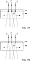
- the layer of cathodoluminescent material 19' is preferably a thin layer, preferably smaller or equal to a maximum depth of the interaction volume, which is arranged on top of and/or supported by a light transmitting support plate 200, as for example shown in figure 7A .
- the layer of cathodoluminescent material 19" is thinner than the maximum depth of the interaction volume, which is also referred to as the scattering range, as shown in figure 7B .
- the use of such a thin layer of cathodoluminescent material 19" is, that signals from higher energy charged particle beams at least substantially do not interfere.
- the layer of cathodoluminescent material 19 is covered with a charge conducting layer 300, as for example shown in figure 8 .
- This charge conducting layer 300 is preferably arranged at a side of said layer of cathodoluminescent material 19 facing the electro-magnetic lens system 13, 14, and preferably is connected to ground potential.
- the charge conducting layer 300 comprises for example a layer of ITO and/or graphene.
- the charge conducting layer 300 comprises a thin metal layer, for example having a thickness of 10 to 20 nm.
- Such a thin metal layer provides the desired charge conducting properties and in addition provides a mirror effect for the photons created in the cathodoluminescent material 19, which mirror effect can increase the part of the created photons which are directed toward the optical arrangement 40 and the detector 20.
- the optical arrangement 40 comprises a lens system 41, 42 which is arranged for imaging said created photons 30, 31 onto the multi-pixel photon detector 20.
- the optical arrangement 40 provides an optical magnification between 5 and 500.
- the apparatus further comprising a system 18 for scanning the focused primary charge particle beams over said sample, and a control-and-signal-processing system 21 for controlling the scanning system 18 and the detector 20, and for analyzing the data from the detector 20 and creating one image per primary charged particle beam.
- the apparatus further comprises a first actuating system 180 for moving the sample holder 150 at a constant speed in a first direction.
- the scanning system 18 as a second actuating system, for scanning the focused primary charged particle beams over said sample in a second direction at least substantially perpendicular to the first direction, the focused primary charged particle beams can be scanned over an area of the surface of the sample 15.
- the control-and-signal-processing system 21 is for example arranged to create one image per primary charged particle beam.
- control-and-signal-processing unit 21 is preferably arranged and/or provided with appropriate subroutines for combining said individual images per primary charged particle beam into one combined image of at least a part of the sample 15.
Landscapes
- Chemical & Material Sciences (AREA)
- Analytical Chemistry (AREA)
- Engineering & Computer Science (AREA)
- Computer Vision & Pattern Recognition (AREA)
- Physics & Mathematics (AREA)
- Electromagnetism (AREA)
- Investigating, Analyzing Materials By Fluorescence Or Luminescence (AREA)
- Analysing Materials By The Use Of Radiation (AREA)
Claims (15)
- Appareil (1) pour inspecter un échantillon (15), dans lequel l'appareil comprend :un porte-échantillon (150) pour porter l'échantillon (15),un générateur de particules chargées en faisceaux multiples (2) pour générer un réseau de faisceaux de particules chargées primaires (3),un système de lentilles électromagnétiques (7, 10, 13, 14) pour diriger ledit réseau de faisceaux de particules chargées primaires (3) dans un réseau de faisceaux de particules chargées primaires focalisés séparés (3, 3', 3") au niveau dudit porte-échantillon (150),un détecteur de photons à pixels multiples (20) agencé pour détecter des photons (30, 31, 32) créés par lesdits faisceaux de particules chargées primaires focalisés (3, 3', 3'') lorsque lesdits faisceaux de particules chargées primaires frappent l'échantillon (15) ou après la transmission desdits faisceaux de particules chargées primaires (23, 23', 23'') à travers l'échantillon, etun ensemble optique (40) pour transporter des photons (30, 31, 32) créés par au moins deux faisceaux de particules chargées primaires focalisés adjacents (3, 3', 3'') dudit réseau de faisceaux de particules chargées primaires focalisés séparés vers des pixels distincts et/ou séparés ou vers des groupes de pixels distincts et/ou séparés du détecteur de photons à pixels multiples (20).
- Appareil selon la revendication 1, dans lequel ledit appareil comprend une couche de matériau cathodoluminescent (19), dans lequel le porte-échantillon (150) est agencé pour positionner l'échantillon (15) entre le système de lentilles électromagnétiques (7, 10, 13, 14) et la couche de matériau cathodoluminescent (19), de sorte que les particules chargées frappent la couche de matériau cathodoluminescent (19) après la transmission à travers ledit échantillon (15).
- Appareil selon la revendication 2, dans lequel la couche de matériau cathodoluminescent (19', 19'') est supportée par une plaque de support transmettant la lumière (200).
- Appareil selon la revendication 2 ou 3, dans lequel ladite couche de matériau cathodoluminescent (19) est recouverte d'une couche conductrice de charge (300), de préférence dans lequel la couche conductrice de charge (300) est agencée au niveau d'un côté de ladite couche de matériau cathodoluminescent (19) faisant face au système de lentilles électromagnétiques (7, 10, 13, 14).
- Appareil selon les revendications 2, 3 ou 4, dans lequel ledit porte-échantillon (150) est agencé pour positionner l'échantillon (15) en contact direct avec et/ou supporté par ladite couche de matériau cathodoluminescent (19).
- Appareil selon les revendications 2, 3 ou 4, dans lequel ledit porte-échantillon (150) est agencé pour positionner l'échantillon (15) à distance de ladite couche de matériau cathodoluminescent (19).
- Appareil selon l'une quelconque des revendications précédentes, dans lequel ledit ensemble optique (40) comprend un système de lentilles qui est agencé pour réaliser des images desdits photons créés (30, 31, 32) sur le détecteur de photons à pixels multiples (20) avec un grossissement optique entre 5 et 500.
- Appareil selon l'une quelconque des revendications précédentes, dans lequel le système de lentilles électromagnétiques (7, 10, 13, 14) est agencé pour projeter un réseau de points séparés sur la surface d'échantillon où les faisceaux de particules chargées primaires focalisés (3, 3', 3") frappent l'échantillon (15) sur le porte-échantillon (150), dans lequel le pas entre les points sur la surface d'échantillon est entre 0,3 et 30 micromètres.
- Appareil selon l'une quelconque des revendications précédentes, dans lequel le détecteur de photons à pixels multiples (20) est une caméra CCD, une caméra CMOS, un réseau de photodiodes à avalanche ou un réseau de photomultiplicateurs.
- Appareil selon la revendication 9, dans lequel la caméra CCD, la caméra CMOS, le réseau de photodiodes à avalanche ou de photomultiplicateurs comprend un réseau de pixels de détecteur est positionné de sorte que le réseau de pixels de détecteur coïncide avec un réseau d'images des points de lumière individuels créés par les faisceaux individuels desdits faisceaux de particules chargées primaires (3, 3', 3").
- Appareil selon l'une quelconque des revendications précédentes, comprenant en outre un système pour scanner les faisceaux de particules chargées primaires focalisés (3, 3', 3'') au-dessus dudit porte-échantillon (150), et un système de commande et de traitement de signaux (21) pour créer une image par faisceau de particules chargées primaire.
- Appareil selon l'une quelconque des revendications précédentes, comprenant en outre un premier système d'actionnement pour déplacer le porte-échantillon (150) à une vitesse constante dans une première direction, et un deuxième système d'actionnement pour scanner les faisceaux de particules chargées primaires focalisés (3, 3', 3'') au-dessus dudit porte-échantillon (150) dans une deuxième direction au moins sensiblement perpendiculaire à la première direction, et un système de commande et de traitement de signaux (21) pour créer une image par faisceau de particules chargées primaire.
- Appareil selon la revendication 11 ou 12, dans lequel ledit appareil comprend en outre une unité de traitement de signaux pour combiner lesdites images individuelles par faisceau de particules chargées primaire en une image combinée d'au moins une partie de l'échantillon.
- Méthode pour inspecter un échantillon (15), utilisant un appareil (1) qui comprend :un porte-échantillon (150) qui porte l'échantillon (15),un générateur de particules chargées en faisceaux multiples (2) qui génère un réseau de faisceaux de particules chargées primaires (3),un système de lentilles électromagnétiques (7, 10, 13, 14) qui dirige ledit réseau de faisceaux de particules chargées primaires (3) dans un réseau de faisceaux de particules chargées primaires focalisés séparés (3, 3', 3'') sur ledit échantillon (15) dans ou sur le porte-échantillon (150),un détecteur de photons à pixels multiples (20) agencé pour détecter des photons (30, 31, 32) créés par lesdits faisceaux de particules chargées primaires focalisés (3, 3', 3'') lorsque lesdits faisceaux de particules chargées primaires frappent l'échantillon (15) ou après la transmission desdits faisceaux de particules chargées primaires (23, 23', 23'') à travers l'échantillon (15), etun ensemble optique (40) qui transporte les photons (30, 31, 32) créés par au moins deux faisceaux de particules chargées primaires focalisés adjacents (3, 3', 3) dudit réseau de faisceaux de particules chargées primaires focalisés séparés vers des pixels distincts et/ou séparés ou vers des groupes de pixels distincts et/ou séparés du détecteur de photons à pixels multiples (20).
- Méthode selon la revendication 14, dans laquelle ledit appareil comprend une couche de matériau cathodoluminescent (19), dans laquelle le porte-échantillon (150) est agencé pour positionner l'échantillon (15) entre le système de lentilles électromagnétiques (7, 10, 13, 14) et la couche de matériau cathodoluminescent (19), dans laquelle les particules chargées qui passent à travers ledit échantillon (15) frappent ensuite la couche de matériau cathodoluminescent (19).
Applications Claiming Priority (2)
| Application Number | Priority Date | Filing Date | Title |
|---|---|---|---|
| NL2012780A NL2012780B1 (en) | 2014-05-08 | 2014-05-08 | Apparatus and method for inspecting a sample using a plurality of charged particle beams. |
| PCT/NL2015/050271 WO2015170969A1 (fr) | 2014-05-08 | 2015-04-23 | Appareil et procédé d'inspection d'échantillon à l'aide d'une pluralité de faisceaux de particules chargées |
Publications (2)
| Publication Number | Publication Date |
|---|---|
| EP3140848A1 EP3140848A1 (fr) | 2017-03-15 |
| EP3140848B1 true EP3140848B1 (fr) | 2018-06-06 |
Family
ID=50981818
Family Applications (1)
| Application Number | Title | Priority Date | Filing Date |
|---|---|---|---|
| EP15726384.9A Active EP3140848B1 (fr) | 2014-05-08 | 2015-04-23 | Appareil et procédé d'inspection d'échantillon à l'aide d'une pluralité de faisceaux de particules chargées |
Country Status (9)
| Country | Link |
|---|---|
| US (1) | US10453649B2 (fr) |
| EP (1) | EP3140848B1 (fr) |
| JP (1) | JP2017515283A (fr) |
| KR (1) | KR102454320B1 (fr) |
| CN (1) | CN106575595B (fr) |
| IL (1) | IL248778A0 (fr) |
| NL (1) | NL2012780B1 (fr) |
| TW (1) | TW201546861A (fr) |
| WO (1) | WO2015170969A1 (fr) |
Families Citing this family (26)
| Publication number | Priority date | Publication date | Assignee | Title |
|---|---|---|---|---|
| US10903042B2 (en) * | 2014-05-08 | 2021-01-26 | Technische Universiteit Delft | Apparatus and method for inspecting a sample using a plurality of charged particle beams |
| DE102015202172B4 (de) | 2015-02-06 | 2017-01-19 | Carl Zeiss Microscopy Gmbh | Teilchenstrahlsystem und Verfahren zur teilchenoptischen Untersuchung eines Objekts |
| JP6834817B2 (ja) * | 2016-08-08 | 2021-02-24 | 株式会社ニューフレアテクノロジー | マルチビーム検査用アパーチャ、マルチビーム用ビーム検査装置、及びマルチ荷電粒子ビーム描画装置 |
| US10141156B2 (en) * | 2016-09-27 | 2018-11-27 | Kla-Tencor Corporation | Measurement of overlay and edge placement errors with an electron beam column array |
| US10453645B2 (en) * | 2016-12-01 | 2019-10-22 | Applied Materials Israel Ltd. | Method for inspecting a specimen and charged particle multi-beam device |
| WO2018145983A1 (fr) * | 2017-02-07 | 2018-08-16 | Asml Netherlands B.V. | Procédé et appareil de détection de particule chargée |
| US10245448B2 (en) * | 2017-07-21 | 2019-04-02 | Varian Medical Systems Particle Therapy Gmbh | Particle beam monitoring systems and methods |
| DE102018202428B3 (de) | 2018-02-16 | 2019-05-09 | Carl Zeiss Microscopy Gmbh | Vielstrahl-Teilchenmikroskop |
| DE102018202421B3 (de) | 2018-02-16 | 2019-07-11 | Carl Zeiss Microscopy Gmbh | Vielstrahl-Teilchenstrahlsystem |
| CN112055886A (zh) | 2018-02-27 | 2020-12-08 | 卡尔蔡司MultiSEM有限责任公司 | 带电粒子多束系统及方法 |
| JP2019164886A (ja) | 2018-03-19 | 2019-09-26 | 株式会社日立ハイテクノロジーズ | ビーム照射装置 |
| US10811215B2 (en) | 2018-05-21 | 2020-10-20 | Carl Zeiss Multisem Gmbh | Charged particle beam system |
| DE102018007455B4 (de) | 2018-09-21 | 2020-07-09 | Carl Zeiss Multisem Gmbh | Verfahren zum Detektorabgleich bei der Abbildung von Objekten mittels eines Mehrstrahl-Teilchenmikroskops, System sowie Computerprogrammprodukt |
| DE102018007652B4 (de) | 2018-09-27 | 2021-03-25 | Carl Zeiss Multisem Gmbh | Teilchenstrahl-System sowie Verfahren zur Stromregulierung von Einzel-Teilchenstrahlen |
| DE102018124044B3 (de) | 2018-09-28 | 2020-02-06 | Carl Zeiss Microscopy Gmbh | Verfahren zum Betreiben eines Vielstrahl-Teilchenstrahlmikroskops und Vielstrahl-Teilchenstrahlsystem |
| CN111477530B (zh) * | 2019-01-24 | 2023-05-05 | 卡尔蔡司MultiSEM有限责任公司 | 利用多束粒子显微镜对3d样本成像的方法 |
| TWI743626B (zh) | 2019-01-24 | 2021-10-21 | 德商卡爾蔡司多重掃描電子顯微鏡有限公司 | 包含多束粒子顯微鏡的系統、對3d樣本逐層成像之方法及電腦程式產品 |
| NL2022755B1 (en) | 2019-03-18 | 2020-09-25 | Univ Delft Tech | Method for inspecting a sample in a charged particle microscope |
| NL2022756B1 (en) | 2019-03-18 | 2020-09-25 | Delmic Ip B V | Integrated optical and charged particle inspection apparatus |
| US20200373115A1 (en) * | 2019-05-23 | 2020-11-26 | Fei Company | Multi-beam scanning electron microscope |
| NL2023249B1 (en) | 2019-06-03 | 2020-12-11 | Delmic Ip B V | Apparatus and method for detecting one or more scanning charged particle beams |
| CN110676149B (zh) * | 2019-09-30 | 2021-06-22 | 南京大学 | 一种电子显微成像系统及成像方法 |
| US11114274B2 (en) * | 2019-12-23 | 2021-09-07 | Carl Zeiss Smt Gmbh | Method and system for testing an integrated circuit |
| NL2024606B1 (en) | 2020-01-06 | 2021-09-07 | Delmic Ip B V | Method and apparatus for inspecting a sample by means of multiple charged particle beamlets |
| EP3882951A1 (fr) * | 2020-03-19 | 2021-09-22 | FEI Company | Dispositif à faisceau de particules chargées pour l'inspection d'un échantillon à l'aide d'une pluralité de faisceaux de particules chargées |
| NL2027636B1 (en) | 2021-02-24 | 2022-09-20 | Univ Delft Tech | Apparatus and method for manipulating thin film sections or ribbons of thin film sections |
Family Cites Families (17)
| Publication number | Priority date | Publication date | Assignee | Title |
|---|---|---|---|---|
| JPH1054878A (ja) | 1996-05-09 | 1998-02-24 | Hitachi Ltd | 蛍光装置およびこれを用いた撮像装置並びに検査装置 |
| JP2001308154A (ja) * | 2000-04-24 | 2001-11-02 | Nikon Corp | 電子線検査装置、電子線検査方法及びデバイス製造方法 |
| JP2003257355A (ja) | 2002-03-04 | 2003-09-12 | Nikon Corp | 走査型電子顕微鏡 |
| US7157703B2 (en) | 2002-08-30 | 2007-01-02 | Ebara Corporation | Electron beam system |
| JP2004095281A (ja) | 2002-08-30 | 2004-03-25 | Ebara Corp | 電子線装置 |
| US7385197B2 (en) | 2004-07-08 | 2008-06-10 | Ebara Corporation | Electron beam apparatus and a device manufacturing method using the same apparatus |
| JP2006066181A (ja) | 2004-08-26 | 2006-03-09 | Ebara Corp | 電子線装置及びそれを用いたデバイス製造方法 |
| EP1843126B1 (fr) | 2005-01-07 | 2009-12-09 | SII NanoTechnology Inc. | Procede et dispositif pour mesurer un echantillon de film mince |
| JP5663717B2 (ja) | 2005-09-06 | 2015-02-04 | カール ツァイス マイクロスコピー ゲーエムベーハーCarl Zeiss Microscopy Gmbh | 荷電粒子システム |
| US7504622B2 (en) * | 2006-04-03 | 2009-03-17 | Applied Materials, Israel, Ltd. | High throughput multi beam detection system and method |
| JP5101845B2 (ja) | 2006-08-21 | 2012-12-19 | エスアイアイ・ナノテクノロジー株式会社 | 集束イオンビーム装置ならびにそれを用いた試料断面作製方法および薄片試料作製方法 |
| WO2008101713A2 (fr) * | 2007-02-22 | 2008-08-28 | Applied Materials Israel Ltd. | Microscope électronique à balayage à fort rendement |
| DE102009046211B4 (de) * | 2009-10-30 | 2017-08-24 | Carl Zeiss Microscopy Gmbh | Detektionsvorrichtung und Teilchenstrahlgerät mit Detektionsvorrichtung |
| NL2009053C2 (en) | 2012-06-22 | 2013-12-24 | Univ Delft Tech | Apparatus and method for inspecting a surface of a sample. |
| JP5936484B2 (ja) | 2012-08-20 | 2016-06-22 | 株式会社日立ハイテクノロジーズ | 荷電粒子線装置及び試料観察方法 |
| NL2009696C2 (en) | 2012-10-25 | 2014-04-29 | Univ Delft Tech | Apparatus and method for inspecting a surface of a sample. |
| EP2879155B1 (fr) * | 2013-12-02 | 2018-04-25 | ICT Integrated Circuit Testing Gesellschaft für Halbleiterprüftechnik mbH | Système multifaisceau EBI à haut rendement |
-
2014
- 2014-05-08 NL NL2012780A patent/NL2012780B1/en active
-
2015
- 2015-04-23 WO PCT/NL2015/050271 patent/WO2015170969A1/fr active Application Filing
- 2015-04-23 EP EP15726384.9A patent/EP3140848B1/fr active Active
- 2015-04-23 CN CN201580036950.2A patent/CN106575595B/zh active Active
- 2015-04-23 JP JP2016566736A patent/JP2017515283A/ja active Pending
- 2015-04-23 US US15/309,748 patent/US10453649B2/en active Active
- 2015-04-23 KR KR1020167033942A patent/KR102454320B1/ko active IP Right Grant
- 2015-05-05 TW TW104114208A patent/TW201546861A/zh unknown
-
2016
- 2016-11-06 IL IL248778A patent/IL248778A0/en unknown
Non-Patent Citations (1)
| Title |
|---|
| None * |
Also Published As
| Publication number | Publication date |
|---|---|
| NL2012780B1 (en) | 2016-02-23 |
| EP3140848A1 (fr) | 2017-03-15 |
| KR20170008764A (ko) | 2017-01-24 |
| IL248778A0 (en) | 2017-01-31 |
| CN106575595B (zh) | 2018-09-25 |
| WO2015170969A1 (fr) | 2015-11-12 |
| KR102454320B1 (ko) | 2022-10-12 |
| TW201546861A (zh) | 2015-12-16 |
| JP2017515283A (ja) | 2017-06-08 |
| CN106575595A (zh) | 2017-04-19 |
| US10453649B2 (en) | 2019-10-22 |
| US20170133198A1 (en) | 2017-05-11 |
Similar Documents
| Publication | Publication Date | Title |
|---|---|---|
| EP3140848B1 (fr) | Appareil et procédé d'inspection d'échantillon à l'aide d'une pluralité de faisceaux de particules chargées | |
| US9449789B2 (en) | Apparatus and method for inspecting a surface of a sample | |
| JP5230063B2 (ja) | 電子ビーム暗視野像形成のための装置および方法 | |
| JP6268169B2 (ja) | サンプルの表面を検査する装置および方法 | |
| CN1222011C (zh) | 一种用于带电粒子束装置的物镜 | |
| JP5179176B2 (ja) | 試料表面を検査する方法、装置、及び蛍光材料の使用 | |
| US10903042B2 (en) | Apparatus and method for inspecting a sample using a plurality of charged particle beams | |
| US7205542B1 (en) | Scanning electron microscope with curved axes | |
| JP2020074331A (ja) | 電子衝撃検出器を動作させる方法 | |
| CN109411320A (zh) | 透射带电粒子显微镜中的衍射图案检测 | |
| EP1389795A2 (fr) | Système de microscopie électronique et méthode d'utilisation | |
| US7842930B2 (en) | Charged particle detector assembly, charged particle beam apparatus and method for generating an image | |
| JP4217565B2 (ja) | 電子顕微鏡用撮像装置 | |
| US9349564B2 (en) | Charged-particle lens that transmits emissions from sample | |
| NL2023249B1 (en) | Apparatus and method for detecting one or more scanning charged particle beams |
Legal Events
| Date | Code | Title | Description |
|---|---|---|---|
| STAA | Information on the status of an ep patent application or granted ep patent |
Free format text: STATUS: THE INTERNATIONAL PUBLICATION HAS BEEN MADE |
|
| PUAI | Public reference made under article 153(3) epc to a published international application that has entered the european phase |
Free format text: ORIGINAL CODE: 0009012 |
|
| STAA | Information on the status of an ep patent application or granted ep patent |
Free format text: STATUS: REQUEST FOR EXAMINATION WAS MADE |
|
| 17P | Request for examination filed |
Effective date: 20161102 |
|
| AK | Designated contracting states |
Kind code of ref document: A1 Designated state(s): AL AT BE BG CH CY CZ DE DK EE ES FI FR GB GR HR HU IE IS IT LI LT LU LV MC MK MT NL NO PL PT RO RS SE SI SK SM TR |
|
| AX | Request for extension of the european patent |
Extension state: BA ME |
|
| DAV | Request for validation of the european patent (deleted) | ||
| DAX | Request for extension of the european patent (deleted) | ||
| REG | Reference to a national code |
Ref country code: DE Ref legal event code: R079 Ref document number: 602015011937 Country of ref document: DE Free format text: PREVIOUS MAIN CLASS: H01J0037280000 Ipc: H01J0037244000 |
|
| GRAP | Despatch of communication of intention to grant a patent |
Free format text: ORIGINAL CODE: EPIDOSNIGR1 |
|
| STAA | Information on the status of an ep patent application or granted ep patent |
Free format text: STATUS: GRANT OF PATENT IS INTENDED |
|
| RIC1 | Information provided on ipc code assigned before grant |
Ipc: H01J 37/244 20060101AFI20171106BHEP Ipc: H01J 37/28 20060101ALI20171106BHEP |
|
| INTG | Intention to grant announced |
Effective date: 20171128 |
|
| GRAJ | Information related to disapproval of communication of intention to grant by the applicant or resumption of examination proceedings by the epo deleted |
Free format text: ORIGINAL CODE: EPIDOSDIGR1 |
|
| STAA | Information on the status of an ep patent application or granted ep patent |
Free format text: STATUS: REQUEST FOR EXAMINATION WAS MADE |
|
| GRAS | Grant fee paid |
Free format text: ORIGINAL CODE: EPIDOSNIGR3 |
|
| STAA | Information on the status of an ep patent application or granted ep patent |
Free format text: STATUS: GRANT OF PATENT IS INTENDED |
|
| GRAP | Despatch of communication of intention to grant a patent |
Free format text: ORIGINAL CODE: EPIDOSNIGR1 |
|
| INTC | Intention to grant announced (deleted) | ||
| GRAA | (expected) grant |
Free format text: ORIGINAL CODE: 0009210 |
|
| STAA | Information on the status of an ep patent application or granted ep patent |
Free format text: STATUS: THE PATENT HAS BEEN GRANTED |
|
| INTG | Intention to grant announced |
Effective date: 20180419 |
|
| AK | Designated contracting states |
Kind code of ref document: B1 Designated state(s): AL AT BE BG CH CY CZ DE DK EE ES FI FR GB GR HR HU IE IS IT LI LT LU LV MC MK MT NL NO PL PT RO RS SE SI SK SM TR |
|
| REG | Reference to a national code |
Ref country code: GB Ref legal event code: FG4D |
|
| REG | Reference to a national code |
Ref country code: CH Ref legal event code: EP Ref country code: AT Ref legal event code: REF Ref document number: 1006983 Country of ref document: AT Kind code of ref document: T Effective date: 20180615 |
|
| REG | Reference to a national code |
Ref country code: IE Ref legal event code: FG4D |
|
| REG | Reference to a national code |
Ref country code: DE Ref legal event code: R096 Ref document number: 602015011937 Country of ref document: DE |
|
| REG | Reference to a national code |
Ref country code: NL Ref legal event code: FP |
|
| REG | Reference to a national code |
Ref country code: LT Ref legal event code: MG4D |
|
| PG25 | Lapsed in a contracting state [announced via postgrant information from national office to epo] |
Ref country code: ES Free format text: LAPSE BECAUSE OF FAILURE TO SUBMIT A TRANSLATION OF THE DESCRIPTION OR TO PAY THE FEE WITHIN THE PRESCRIBED TIME-LIMIT Effective date: 20180606 Ref country code: LT Free format text: LAPSE BECAUSE OF FAILURE TO SUBMIT A TRANSLATION OF THE DESCRIPTION OR TO PAY THE FEE WITHIN THE PRESCRIBED TIME-LIMIT Effective date: 20180606 Ref country code: CY Free format text: LAPSE BECAUSE OF FAILURE TO SUBMIT A TRANSLATION OF THE DESCRIPTION OR TO PAY THE FEE WITHIN THE PRESCRIBED TIME-LIMIT Effective date: 20180606 Ref country code: NO Free format text: LAPSE BECAUSE OF FAILURE TO SUBMIT A TRANSLATION OF THE DESCRIPTION OR TO PAY THE FEE WITHIN THE PRESCRIBED TIME-LIMIT Effective date: 20180906 Ref country code: BG Free format text: LAPSE BECAUSE OF FAILURE TO SUBMIT A TRANSLATION OF THE DESCRIPTION OR TO PAY THE FEE WITHIN THE PRESCRIBED TIME-LIMIT Effective date: 20180906 Ref country code: SE Free format text: LAPSE BECAUSE OF FAILURE TO SUBMIT A TRANSLATION OF THE DESCRIPTION OR TO PAY THE FEE WITHIN THE PRESCRIBED TIME-LIMIT Effective date: 20180606 Ref country code: FI Free format text: LAPSE BECAUSE OF FAILURE TO SUBMIT A TRANSLATION OF THE DESCRIPTION OR TO PAY THE FEE WITHIN THE PRESCRIBED TIME-LIMIT Effective date: 20180606 |
|
| PG25 | Lapsed in a contracting state [announced via postgrant information from national office to epo] |
Ref country code: HR Free format text: LAPSE BECAUSE OF FAILURE TO SUBMIT A TRANSLATION OF THE DESCRIPTION OR TO PAY THE FEE WITHIN THE PRESCRIBED TIME-LIMIT Effective date: 20180606 Ref country code: GR Free format text: LAPSE BECAUSE OF FAILURE TO SUBMIT A TRANSLATION OF THE DESCRIPTION OR TO PAY THE FEE WITHIN THE PRESCRIBED TIME-LIMIT Effective date: 20180907 Ref country code: LV Free format text: LAPSE BECAUSE OF FAILURE TO SUBMIT A TRANSLATION OF THE DESCRIPTION OR TO PAY THE FEE WITHIN THE PRESCRIBED TIME-LIMIT Effective date: 20180606 Ref country code: RS Free format text: LAPSE BECAUSE OF FAILURE TO SUBMIT A TRANSLATION OF THE DESCRIPTION OR TO PAY THE FEE WITHIN THE PRESCRIBED TIME-LIMIT Effective date: 20180606 |
|
| REG | Reference to a national code |
Ref country code: AT Ref legal event code: MK05 Ref document number: 1006983 Country of ref document: AT Kind code of ref document: T Effective date: 20180606 |
|
| PG25 | Lapsed in a contracting state [announced via postgrant information from national office to epo] |
Ref country code: RO Free format text: LAPSE BECAUSE OF FAILURE TO SUBMIT A TRANSLATION OF THE DESCRIPTION OR TO PAY THE FEE WITHIN THE PRESCRIBED TIME-LIMIT Effective date: 20180606 Ref country code: PL Free format text: LAPSE BECAUSE OF FAILURE TO SUBMIT A TRANSLATION OF THE DESCRIPTION OR TO PAY THE FEE WITHIN THE PRESCRIBED TIME-LIMIT Effective date: 20180606 Ref country code: SK Free format text: LAPSE BECAUSE OF FAILURE TO SUBMIT A TRANSLATION OF THE DESCRIPTION OR TO PAY THE FEE WITHIN THE PRESCRIBED TIME-LIMIT Effective date: 20180606 Ref country code: AT Free format text: LAPSE BECAUSE OF FAILURE TO SUBMIT A TRANSLATION OF THE DESCRIPTION OR TO PAY THE FEE WITHIN THE PRESCRIBED TIME-LIMIT Effective date: 20180606 Ref country code: EE Free format text: LAPSE BECAUSE OF FAILURE TO SUBMIT A TRANSLATION OF THE DESCRIPTION OR TO PAY THE FEE WITHIN THE PRESCRIBED TIME-LIMIT Effective date: 20180606 Ref country code: IS Free format text: LAPSE BECAUSE OF FAILURE TO SUBMIT A TRANSLATION OF THE DESCRIPTION OR TO PAY THE FEE WITHIN THE PRESCRIBED TIME-LIMIT Effective date: 20181006 |
|
| PG25 | Lapsed in a contracting state [announced via postgrant information from national office to epo] |
Ref country code: IT Free format text: LAPSE BECAUSE OF FAILURE TO SUBMIT A TRANSLATION OF THE DESCRIPTION OR TO PAY THE FEE WITHIN THE PRESCRIBED TIME-LIMIT Effective date: 20180606 Ref country code: SM Free format text: LAPSE BECAUSE OF FAILURE TO SUBMIT A TRANSLATION OF THE DESCRIPTION OR TO PAY THE FEE WITHIN THE PRESCRIBED TIME-LIMIT Effective date: 20180606 |
|
| REG | Reference to a national code |
Ref country code: DE Ref legal event code: R097 Ref document number: 602015011937 Country of ref document: DE |
|
| PLBE | No opposition filed within time limit |
Free format text: ORIGINAL CODE: 0009261 |
|
| STAA | Information on the status of an ep patent application or granted ep patent |
Free format text: STATUS: NO OPPOSITION FILED WITHIN TIME LIMIT |
|
| 26N | No opposition filed |
Effective date: 20190307 |
|
| PG25 | Lapsed in a contracting state [announced via postgrant information from national office to epo] |
Ref country code: DK Free format text: LAPSE BECAUSE OF FAILURE TO SUBMIT A TRANSLATION OF THE DESCRIPTION OR TO PAY THE FEE WITHIN THE PRESCRIBED TIME-LIMIT Effective date: 20180606 Ref country code: SI Free format text: LAPSE BECAUSE OF FAILURE TO SUBMIT A TRANSLATION OF THE DESCRIPTION OR TO PAY THE FEE WITHIN THE PRESCRIBED TIME-LIMIT Effective date: 20180606 |
|
| PG25 | Lapsed in a contracting state [announced via postgrant information from national office to epo] |
Ref country code: AL Free format text: LAPSE BECAUSE OF FAILURE TO SUBMIT A TRANSLATION OF THE DESCRIPTION OR TO PAY THE FEE WITHIN THE PRESCRIBED TIME-LIMIT Effective date: 20180606 |
|
| REG | Reference to a national code |
Ref country code: CH Ref legal event code: PL |
|
| REG | Reference to a national code |
Ref country code: BE Ref legal event code: MM Effective date: 20190430 |
|
| PG25 | Lapsed in a contracting state [announced via postgrant information from national office to epo] |
Ref country code: MC Free format text: LAPSE BECAUSE OF FAILURE TO SUBMIT A TRANSLATION OF THE DESCRIPTION OR TO PAY THE FEE WITHIN THE PRESCRIBED TIME-LIMIT Effective date: 20180606 Ref country code: LU Free format text: LAPSE BECAUSE OF NON-PAYMENT OF DUE FEES Effective date: 20190423 |
|
| PG25 | Lapsed in a contracting state [announced via postgrant information from national office to epo] |
Ref country code: CH Free format text: LAPSE BECAUSE OF NON-PAYMENT OF DUE FEES Effective date: 20190430 Ref country code: LI Free format text: LAPSE BECAUSE OF NON-PAYMENT OF DUE FEES Effective date: 20190430 |
|
| PG25 | Lapsed in a contracting state [announced via postgrant information from national office to epo] |
Ref country code: BE Free format text: LAPSE BECAUSE OF NON-PAYMENT OF DUE FEES Effective date: 20190430 |
|
| PG25 | Lapsed in a contracting state [announced via postgrant information from national office to epo] |
Ref country code: TR Free format text: LAPSE BECAUSE OF FAILURE TO SUBMIT A TRANSLATION OF THE DESCRIPTION OR TO PAY THE FEE WITHIN THE PRESCRIBED TIME-LIMIT Effective date: 20180606 |
|
| PG25 | Lapsed in a contracting state [announced via postgrant information from national office to epo] |
Ref country code: IE Free format text: LAPSE BECAUSE OF NON-PAYMENT OF DUE FEES Effective date: 20190423 |
|
| PG25 | Lapsed in a contracting state [announced via postgrant information from national office to epo] |
Ref country code: PT Free format text: LAPSE BECAUSE OF FAILURE TO SUBMIT A TRANSLATION OF THE DESCRIPTION OR TO PAY THE FEE WITHIN THE PRESCRIBED TIME-LIMIT Effective date: 20181008 |
|
| PG25 | Lapsed in a contracting state [announced via postgrant information from national office to epo] |
Ref country code: HU Free format text: LAPSE BECAUSE OF FAILURE TO SUBMIT A TRANSLATION OF THE DESCRIPTION OR TO PAY THE FEE WITHIN THE PRESCRIBED TIME-LIMIT; INVALID AB INITIO Effective date: 20150423 Ref country code: MT Free format text: LAPSE BECAUSE OF FAILURE TO SUBMIT A TRANSLATION OF THE DESCRIPTION OR TO PAY THE FEE WITHIN THE PRESCRIBED TIME-LIMIT Effective date: 20180606 |
|
| PG25 | Lapsed in a contracting state [announced via postgrant information from national office to epo] |
Ref country code: MK Free format text: LAPSE BECAUSE OF FAILURE TO SUBMIT A TRANSLATION OF THE DESCRIPTION OR TO PAY THE FEE WITHIN THE PRESCRIBED TIME-LIMIT Effective date: 20180606 |
|
| P01 | Opt-out of the competence of the unified patent court (upc) registered |
Effective date: 20230517 |
|
| PGFP | Annual fee paid to national office [announced via postgrant information from national office to epo] |
Ref country code: FR Payment date: 20230421 Year of fee payment: 9 Ref country code: DE Payment date: 20230427 Year of fee payment: 9 Ref country code: CZ Payment date: 20230421 Year of fee payment: 9 |
|
| PGFP | Annual fee paid to national office [announced via postgrant information from national office to epo] |
Ref country code: GB Payment date: 20230418 Year of fee payment: 9 |
|
| PGFP | Annual fee paid to national office [announced via postgrant information from national office to epo] |
Ref country code: NL Payment date: 20240425 Year of fee payment: 10 |