EP3125285B1 - Pad-array-struktur auf einem substrat zur montage eines ic-chips auf einem substrat und optisches modul mit dieser pad-array-struktur - Google Patents
Pad-array-struktur auf einem substrat zur montage eines ic-chips auf einem substrat und optisches modul mit dieser pad-array-struktur Download PDFInfo
- Publication number
- EP3125285B1 EP3125285B1 EP15769376.3A EP15769376A EP3125285B1 EP 3125285 B1 EP3125285 B1 EP 3125285B1 EP 15769376 A EP15769376 A EP 15769376A EP 3125285 B1 EP3125285 B1 EP 3125285B1
- Authority
- EP
- European Patent Office
- Prior art keywords
- column
- pads
- pad
- signal
- pad array
- Prior art date
- Legal status (The legal status is an assumption and is not a legal conclusion. Google has not performed a legal analysis and makes no representation as to the accuracy of the status listed.)
- Active
Links
Images


Classifications
-
- H—ELECTRICITY
- H05—ELECTRIC TECHNIQUES NOT OTHERWISE PROVIDED FOR
- H05K—PRINTED CIRCUITS; CASINGS OR CONSTRUCTIONAL DETAILS OF ELECTRIC APPARATUS; MANUFACTURE OF ASSEMBLAGES OF ELECTRICAL COMPONENTS
- H05K1/00—Printed circuits
- H05K1/02—Details
- H05K1/11—Printed elements for providing electric connections to or between printed circuits
- H05K1/111—Pads for surface mounting, e.g. lay-out
-
- G—PHYSICS
- G02—OPTICS
- G02B—OPTICAL ELEMENTS, SYSTEMS OR APPARATUS
- G02B6/00—Light guides; Structural details of arrangements comprising light guides and other optical elements, e.g. couplings
- G02B6/10—Light guides; Structural details of arrangements comprising light guides and other optical elements, e.g. couplings of the optical waveguide type
- G02B6/12—Light guides; Structural details of arrangements comprising light guides and other optical elements, e.g. couplings of the optical waveguide type of the integrated circuit kind
- G02B6/122—Basic optical elements, e.g. light-guiding paths
-
- G—PHYSICS
- G02—OPTICS
- G02B—OPTICAL ELEMENTS, SYSTEMS OR APPARATUS
- G02B6/00—Light guides; Structural details of arrangements comprising light guides and other optical elements, e.g. couplings
- G02B6/24—Coupling light guides
- G02B6/42—Coupling light guides with opto-electronic elements
- G02B6/4201—Packages, e.g. shape, construction, internal or external details
- G02B6/4219—Mechanical fixtures for holding or positioning the elements relative to each other in the couplings; Alignment methods for the elements, e.g. measuring or observing methods especially used therefor
- G02B6/4228—Passive alignment, i.e. without a detection of the degree of coupling or the position of the elements
- G02B6/4232—Passive alignment, i.e. without a detection of the degree of coupling or the position of the elements using the surface tension of fluid solder to align the elements, e.g. solder bump techniques
-
- H—ELECTRICITY
- H05—ELECTRIC TECHNIQUES NOT OTHERWISE PROVIDED FOR
- H05K—PRINTED CIRCUITS; CASINGS OR CONSTRUCTIONAL DETAILS OF ELECTRIC APPARATUS; MANUFACTURE OF ASSEMBLAGES OF ELECTRICAL COMPONENTS
- H05K1/00—Printed circuits
- H05K1/02—Details
- H05K1/0213—Electrical arrangements not otherwise provided for
- H05K1/0216—Reduction of cross-talk, noise or electromagnetic interference
- H05K1/0218—Reduction of cross-talk, noise or electromagnetic interference by printed shielding conductors, ground planes or power plane
- H05K1/0219—Printed shielding conductors for shielding around or between signal conductors, e.g. coplanar or coaxial printed shielding conductors
-
- H—ELECTRICITY
- H05—ELECTRIC TECHNIQUES NOT OTHERWISE PROVIDED FOR
- H05K—PRINTED CIRCUITS; CASINGS OR CONSTRUCTIONAL DETAILS OF ELECTRIC APPARATUS; MANUFACTURE OF ASSEMBLAGES OF ELECTRICAL COMPONENTS
- H05K1/00—Printed circuits
- H05K1/02—Details
- H05K1/0213—Electrical arrangements not otherwise provided for
- H05K1/0237—High frequency adaptations
- H05K1/0245—Lay-out of balanced signal pairs, e.g. differential lines or twisted lines
-
- H—ELECTRICITY
- H05—ELECTRIC TECHNIQUES NOT OTHERWISE PROVIDED FOR
- H05K—PRINTED CIRCUITS; CASINGS OR CONSTRUCTIONAL DETAILS OF ELECTRIC APPARATUS; MANUFACTURE OF ASSEMBLAGES OF ELECTRICAL COMPONENTS
- H05K1/00—Printed circuits
- H05K1/18—Printed circuits structurally associated with non-printed electric components
- H05K1/181—Printed circuits structurally associated with non-printed electric components associated with surface mounted components
-
- H—ELECTRICITY
- H10—SEMICONDUCTOR DEVICES; ELECTRIC SOLID-STATE DEVICES NOT OTHERWISE PROVIDED FOR
- H10W—GENERIC PACKAGES, INTERCONNECTIONS, CONNECTORS OR OTHER CONSTRUCTIONAL DETAILS OF DEVICES COVERED BY CLASS H10
- H10W70/00—Package substrates; Interposers; Redistribution layers [RDL]
- H10W70/60—Insulating or insulated package substrates; Interposers; Redistribution layers
- H10W70/62—Insulating or insulated package substrates; Interposers; Redistribution layers characterised by their interconnections
- H10W70/65—Shapes or dispositions of interconnections
- H10W70/658—Shapes or dispositions of interconnections for devices provided for in groups H10D8/00 - H10D48/00
-
- H—ELECTRICITY
- H05—ELECTRIC TECHNIQUES NOT OTHERWISE PROVIDED FOR
- H05K—PRINTED CIRCUITS; CASINGS OR CONSTRUCTIONAL DETAILS OF ELECTRIC APPARATUS; MANUFACTURE OF ASSEMBLAGES OF ELECTRICAL COMPONENTS
- H05K1/00—Printed circuits
- H05K1/02—Details
- H05K1/0213—Electrical arrangements not otherwise provided for
- H05K1/0237—High frequency adaptations
- H05K1/0243—Printed circuits associated with mounted high frequency components
-
- H—ELECTRICITY
- H05—ELECTRIC TECHNIQUES NOT OTHERWISE PROVIDED FOR
- H05K—PRINTED CIRCUITS; CASINGS OR CONSTRUCTIONAL DETAILS OF ELECTRIC APPARATUS; MANUFACTURE OF ASSEMBLAGES OF ELECTRICAL COMPONENTS
- H05K1/00—Printed circuits
- H05K1/02—Details
- H05K1/0213—Electrical arrangements not otherwise provided for
- H05K1/0237—High frequency adaptations
- H05K1/025—Impedance arrangements, e.g. impedance matching, reduction of parasitic impedance
- H05K1/0251—Impedance arrangements, e.g. impedance matching, reduction of parasitic impedance related to vias or transitions between vias and transmission lines
-
- H—ELECTRICITY
- H05—ELECTRIC TECHNIQUES NOT OTHERWISE PROVIDED FOR
- H05K—PRINTED CIRCUITS; CASINGS OR CONSTRUCTIONAL DETAILS OF ELECTRIC APPARATUS; MANUFACTURE OF ASSEMBLAGES OF ELECTRICAL COMPONENTS
- H05K2201/00—Indexing scheme relating to printed circuits covered by H05K1/00
- H05K2201/10—Details of components or other objects attached to or integrated in a printed circuit board
- H05K2201/10007—Types of components
- H05K2201/10121—Optical component, e.g. opto-electronic component
-
- H—ELECTRICITY
- H05—ELECTRIC TECHNIQUES NOT OTHERWISE PROVIDED FOR
- H05K—PRINTED CIRCUITS; CASINGS OR CONSTRUCTIONAL DETAILS OF ELECTRIC APPARATUS; MANUFACTURE OF ASSEMBLAGES OF ELECTRICAL COMPONENTS
- H05K2201/00—Indexing scheme relating to printed circuits covered by H05K1/00
- H05K2201/10—Details of components or other objects attached to or integrated in a printed circuit board
- H05K2201/10613—Details of electrical connections of non-printed components, e.g. special leads
- H05K2201/10621—Components characterised by their electrical contacts
- H05K2201/10734—Ball grid array [BGA]; Bump grid array
-
- H—ELECTRICITY
- H05—ELECTRIC TECHNIQUES NOT OTHERWISE PROVIDED FOR
- H05K—PRINTED CIRCUITS; CASINGS OR CONSTRUCTIONAL DETAILS OF ELECTRIC APPARATUS; MANUFACTURE OF ASSEMBLAGES OF ELECTRICAL COMPONENTS
- H05K3/00—Apparatus or processes for manufacturing printed circuits
- H05K3/46—Manufacturing multilayer circuits
- H05K3/4688—Composite multilayer circuits, i.e. comprising insulating layers having different properties
-
- H—ELECTRICITY
- H10—SEMICONDUCTOR DEVICES; ELECTRIC SOLID-STATE DEVICES NOT OTHERWISE PROVIDED FOR
- H10W—GENERIC PACKAGES, INTERCONNECTIONS, CONNECTORS OR OTHER CONSTRUCTIONAL DETAILS OF DEVICES COVERED BY CLASS H10
- H10W90/00—Package configurations
- H10W90/701—Package configurations characterised by the relative positions of pads or connectors relative to package parts
- H10W90/721—Package configurations characterised by the relative positions of pads or connectors relative to package parts of bump connectors
- H10W90/724—Package configurations characterised by the relative positions of pads or connectors relative to package parts of bump connectors between a chip and a stacked insulating package substrate, interposer or RDL
-
- Y—GENERAL TAGGING OF NEW TECHNOLOGICAL DEVELOPMENTS; GENERAL TAGGING OF CROSS-SECTIONAL TECHNOLOGIES SPANNING OVER SEVERAL SECTIONS OF THE IPC; TECHNICAL SUBJECTS COVERED BY FORMER USPC CROSS-REFERENCE ART COLLECTIONS [XRACs] AND DIGESTS
- Y02—TECHNOLOGIES OR APPLICATIONS FOR MITIGATION OR ADAPTATION AGAINST CLIMATE CHANGE
- Y02P—CLIMATE CHANGE MITIGATION TECHNOLOGIES IN THE PRODUCTION OR PROCESSING OF GOODS
- Y02P70/00—Climate change mitigation technologies in the production process for final industrial or consumer products
- Y02P70/50—Manufacturing or production processes characterised by the final manufactured product
Definitions
- the present invention relates to a pad array structure on a substrate for installing an IC chip on the substrate; and, more specifically, the present invention relates to a pad array structure, specifically, a pad array structure for an IC chip on a substrate, that is characterized in relationships between ground pads and signal pads in terms of arrangement thereof in the pad array structure.
- the present invention relates to an optical module comprising a pad array structure, such as that described above, formed on a chip by means of a silicon-photonics technique.
- optical elements such as a semiconductor laser, a photodiode, or the like that performs photoelectric conversion is included as a package within the optical module, and a part of the package comprises a ceramic substrate.
- the ceramic substrate comprises a multilayer structure; and conductor patterns and ground conductors, through which signals propagate, are patterned within the substrate or on the surface of the substrate in such a manner that the conductor patterns and the ground conductors do not cross each other.
- a general factor that makes the patterning structure complicated is that a pattern for high-speed signals and a pattern for ground are placed in proximity to each other in an optical module.
- an optical module in Patent-related Document 1 Fig. 1 of Patent-related Document 1
- two lead pins for high-speed signals are arranged in proximity to each other, and lead pins for ground are arranged beside the pair of the two lead pins.
- a signal input/output part that is used for transmission of differential signals and has a GSSG (GND-SIGNAL-SIGNAL-GND) structure is shown, and it is to be connected to a conductor pad or a ground pad through vias within a multilayer substrate.
- Non-patent-related Document 1 there is another recent example of a prior-art optical module, wherein a silicon photonics technique is used for integrating and arranging a driver IC on a silicon-photonics chip, for the purposes of downsizing of a chip and reduction of electric power consumption.
- a silicon photonics technique is used for integrating and arranging a driver IC on a silicon-photonics chip, for the purposes of downsizing of a chip and reduction of electric power consumption.
- respective optical elements such as a semiconductor laser and so on are also installed on the silicon-photonics chip, increasing of the number of parts is inevitable.
- it is necessary to take into consideration when designing a pad array region for connecting with the IC on a silicon-photonics chip, the matters such that (i) the degree of freedom is very low, and (ii) crossing of electric wires has to be avoided.
- Patent-related Document 1 JP Patent Application Public Disclosure No. 2012-047823 . Furthermore US 2011/0093828 A1 describes a pin-out designation method for package-board codesign and shows the preamble of claim 1. US 6,384,341 B1 describes a multi-layer circuit board that simultaneously optimizes impedance and interference within the multi-layer circuit board and a controlled impedance connector to which it is attached.
- Non-patent-related Document 1 " Demonstration of 12.5-Gbps optical interconnections integrated with lasers, optical splitters, optical modulators and photodetectors on a single silicon substrate," OPTICS EXPRESS, Vol. 20, No. 26 (1012/12/10), B256-B263
- An object of the present invention is to realize, in a pad array arrangement structure on a substrate for installing an IC chip on the substrate, a structure that avoids using multilayered wiring on a substrate by devising arrangement of pads on a pad array region for an IC. Further, another object of the present invention is to apply the pad array arrangement structure to an optical module, especially, to a dense, multichannel optical module to which a silicon photonics technique is applied.
- the present invention is defined in claim 1. It provides a pad array structure on a substrate for installing an IC chip on the substrate. Further, it is characterized in that a first peripheral part of a pad array region comprises: plural ground pads, wherein the ground pads are arranged in a first column, with equal distances between adjacent ground pads; and plural signal pads, wherein the signal pads are arranged in a second column that is positioned at an inward side of and in parallel with the first column, with equal distances between adjacent signal pads; wherein each of the signal pads extends through a place between two adjacent ground pads in the first column and connects to an external circuit on the substrate, so that an electric signal is inputted from the external circuit to the signal pad or outputted from the signal pad to the external circuit.
- the plural signal pads are set to constitute plural pairs of differential signal pads, and each of the ground pads in the first column in the first peripheral part is arranged in a place between adjacent two pairs of the differential signal pads in the second column in the first peripheral part. Further, at least one of the ground pads in the first column in the first peripheral part is arranged in a place corresponding to a center between adjacent two pairs of the differential signal pads in the second column in the first peripheral part.
- An embodiment of the present invention provides an optical module comprising the pad array structure. Further, it is characterized in that the IC chip is installed on an opto-electric hybrid board, and that the IC chip is one of a driver IC for driving an optical device, a receiver (receiving device) IC for receiving an optical signal, and a transmitter (transmitting device) IC for transmitting an optical signal.
- the IC chip is installed on an opto-electric hybrid board, and that the IC chip is one of a driver IC for driving an optical device, a receiver (receiving device) IC for receiving an optical signal, and a transmitter (transmitting device) IC for transmitting an optical signal.
- a pad array arrangement structure formed on a substrate will be explained with reference to the figures.
- the pad array arrangement structure on a substrate is not limited to the above, and the pad array arrangement structure is similarly applicable to a receiver (a receiving device) for receiving an optical signal and a transceiver (a transmitting device) for transmitting an optical signal on an opto-electric hybrid board in an optical module.
- the pad array arrangement structure according to the present invention is also applicable to a silicon interposer having a similar pad array structure, for example. Also, note that similar reference symbols are assigned to similar components in the figures.
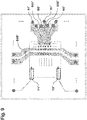
- Fig. 1 is a top view showing an example of arrangement of a pad array on an opto-electric hybrid board of an optical module and wiring relating thereto, according to the above explained prior-art technique.
- the inside of a dashed line region is a pad array region 10, and part of arrangement of various types of pads is enlarged and shown.
- the prior-art pad array arrangement it is necessary to use a multilayered wiring structure for wiring.
- an "S" column 11, a “G” column 12, a “V” column 13, and a “G” column 14 are arranged in parallel with each other in this order.
- the "S” column 11 comprises plural signal pads (S), that are arranged with equal distances therebetween, for making high frequency signals propagate through high-speed signal wires 15.
- Plural signal pads (S) are configured to constitute pairs of differential signal pads.
- the signal wire 15 is connected to an external circuit via a high-speed signal pad (not shown) formed on a substrate, so that a differential electric signal is inputted from the external circuit to the signal pad or outputted from the signal pad to the external circuit.
- the "G” column 12 is arranged to be positioned at an inward side of and in parallel with the "S" column 11, and comprises plural ground pads (G) that are arranged with equal distances therebetween.
- Each ground pad (G) is connected to a ground wire 16, and connected to a ground pad (not shown) formed on the substrate.
- the ground wire 16 is generally required to be positioned in proximity to the signal wire 15 for maintaining a characteristic impedance during propagation of a high frequency signal.
- the "V" column 13 and the "G” column 14, that are arrange in parallel with each other, comprise plural electric-power-source voltage pads and plural ground pads, respectively.
- the "G" column 14 in this example is connected to the "G" column 12 (connection is not shown).
- the line width of the ground wire 16 is made to be substantially wider than that of the signal wire 15, and the area of the ground wire 16 is thus made to be several-tens-of-times larger than that of the signal wire 15.
- the ground wire 16 overlaps a part of the signal pad arrangement section and a part of the signal wire 15, so that the wiring rule cannot be satisfied.
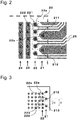
- Fig. 2 is a top view showing an example of a pad array arrangement structure on a substrate and wiring relating thereto, according to an embodiment of the present invention, wherein the structure is devised for avoiding adoption of multilayered wiring such as that shown in Fig. 1 .
- the inside of a dashed line region is a pad array region 20, and part of arrangement of various types of pads are enlarged and shown in a manner similar to that of Fig. 1 .
- a "G” column 21, an "S” column 22, a “G” column 23, and a “V” column 24 are arranged in this order.
- plural ground pads are arranged with equal distances therebetween; and, in the "S” column 22 that is adjacent to and in parallel with the "G” column 21, plural signal pads are arranged with equal distances therebetween.
- the "S" column 22 is positioned at an inward side of the "G” column 21. Further, a signal wire 25 extending from each signal pad in the "S” column 22 extends through a space between two adjacent ground pads 211 and 212 in the "G” column 21, and connects to an external circuit on the substrate via a high-speed signal pad (not shown) formed on the substrate, for inputting an electric signal from the external circuit to the signal pad or outputting an electric signal from the signal pad to the external circuit.
- each ground pad in the "G" column 21 is positioned in a place corresponding to a place (especially, a middle place) between two adjacent differential signal pad pairs in the "S" column 22.
- the ground pad 211 is positioned in a place corresponding to a middle point between the differential signal pad pairs 22a and 22b, as shown in the figure.
- the pad array structure By making the pad array structure to have the above construction, overlapping between signal wires and ground wires, such as that observed in Fig. 1 , does not appear in relation to arrangement of respective pads in the "G" column 21 and the "S" column 22 and wiring relating thereto; thus, use of the multilayered wiring structure can be avoided, i.e., the pad array structure can be realized by use of a single-layer wiring. As a result thereof, the wiring resistance of the IC electric-power-source wiring can be notably reduced.
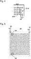
- Fig. 3 shows, by scaling the drawing of the IC pad array region 20 in Fig. 2 , the pad array (a part thereof) of the IC pad array region 20.
- the ground pad 212 is positioned in a place corresponding to a middle place between two adjacent differential signal pad pairs 22a and 22b in the "S" column 22.
- the pitch d1 between two ground pads 212 and 213 is exactly twice the pitch between the two differential pads 223 and 224.
- each ground pad in the "G" column 21 is positioned in a place corresponding to a middle place between two adjacent differential signal pad pairs in the "S" column 22 in each of Figs. 2 and 3 , the position is not limited to that explained above.
- a ground pad 212' in a "G" column 21' may be positioned in a place corresponding to a place of one of signal pads in a differential signal pad pair 22b' (223' in this example); that is, the pads may be arranged in a grid form.
- any form of arrangement may be possible, as long as each pad is arranged in such a manner that each signal wire extending from each signal pad in the "S" column extends through a place between two adjacent ground pads in the "G” column, and that each wire is arranged accordingly.
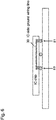
- Fig. 5 is a top view showing the whole IC pad array region 20 shown in each of Figs. 2 and 3 , according to an embodiment of the present invention.
- the above "G" column 21, "S" column 22, ... correspond to those from a side (the right side in this example) of the peripheral part of the IC pad array region 20.
- plural IC control pads may be further arranged at a left-side peripheral part that is located opposite to the right-side peripheral part, especially, at regions 28 and 29 positioned at places located near the inward side of both ends of the left-side peripheral part.
- the wiring structure for connecting the IC control pads in the IC pad array region 20 and corresponding IC control pads (not shown) in the substrate is constructed based on consideration such that it is preferable to have a distance between the wiring structure and the single-layer wiring structure of the part of the "S" column 22 and the "G" column 21 in each of Figs 2 and 3 as much as possible, in view of design such that it is general to adopt a multilayered wiring structure as the wiring structure for connection between the IC control pads in the IC pad array region 20 and corresponding IC control pads (not shown) in the substrate.
- the wiring structure can be simplified.
- the distances between the IC control pads and the IC electric-power-source pads can be reduced by arranging, in the IC pad array region, the arranged columns 26 and 27 of the IC electric-power-source pads in such a manner that the two columns are adjacently positioned in parallel with each other, at the outward side of the IC control pad arrangement region in the left-side peripheral part; and, as a result thereof, the structure can be further simplified.
- a single-layer structure should be used also, by considering avoidance of adoption of a multilayered wiring structure in the part of the IC electric-power-source pads.
- Fig. 2 will be referred to again.
- the "G" column and the "V” column are arranged in this order at the inward side of the "G” column 21 and the "S” column 22.
- the positional relationship between the "G” column 23 and the "V” column 24 is opposite to the other.
- the reason to arrange the "G” column 23 at a place inside and proximity to the "S” column 22 in a manner of the above embodiment is to take necessity to connect the respective ground pads in the "G” column 23 to the respective ground pads in the "G” column 21 into consideration; and, in this regard, by adopting arrangement such as that shown in Fig. 2 , the distance between the "G” column 23 and the "G” column 21 can be reduced.
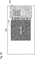
- Fig. 6 shows a schematic cross-section view of a substrate and an IC chip installed on the substrate
- Fig. 7 shows an example of a schematic top view corresponding to Fig. 6 .
- ground wires 30 are provided at an IC-chip side and connection between the ground pads (specifically, connection between the ground pads in the "G” column 21 and the ground pads in the "G” column 23, and connection between adjacent ground pads in the "G” column 21) are made by the IC-chip-side ground wires 30 in the above manner, adoption of a multilayered wiring structure in the substrate can be avoided. Note that the embodiment of arrangement of the respective pads shown above is a mere example.
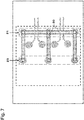
- Fig. 8 is an example of a drawing of an element arrangement region on an opto-electric hybrid board 100 in an optical module, in the case that an IC pad array structure according to the present invention constructed in the above manner is applied to the optical module.
- the IC chip in the optical module is installed on the opto-electric hybrid board, and is one of a driver IC for driving an optical device, a receiver (receiving device) IC for receiving an optical signal, and a transceiver (transmitting device) IC for transmitting an optical signal.
- the drawing of the element arrangement region on an opto-electric hybrid board 100 shown in Fig. 8 can be used as a drawing of an element arrangement region on an opto-electric hybrid board that is constructed as an optical transmitter or a transmitting part of a transceiver.
- the wiring structure can be simplified and the multilayered wiring structure can be minimized.
- the dashed line regions 71 and 72 comprise multilayered wiring structures, and other regions can be realized as those comprising single-layer structures.
- the reason that the dashed line regions 71 and 72 comprise multilayered wiring structures is that the IC control wires extending from the pad array region 20 to the IC control pads 52 cross the electric-power-source (reinforced) wire 505 and the ground (reinforced) wire 503, as shown in the figure.
- the number of vias to be used for connection between layers can be reduced and, thus, the wiring resistance of the IC electric-power-source wires due to the vias can be reduced.
- Fig. 9 shows a different modification of a drawing of an element arrangement region on an opto-electric hybrid board 100 in an optical module, in the case that an IC pad array structure according to the present invention is applied to the optical module.
- the ground (reinforced) wire 503 is removed, and arrangement of the electric-power-source (reinforced) wire 505' is limited in a certain way. It is understandable, in the drawing of the element arrangement region shown in Fig. 9 , that the whole wiring structure including the dashed line regions 71' and 72' can be realized as a single layer structure, by adopting such an arrangement construction described above.
- the part of the ground wire 502' is also modified.
- the IC pad array structure according to the present invention can be applicable, when an opto-electric hybrid board (a silicon substrate) is connected to a printed circuit board, as an electrode pattern used for connection between these elements.
- the arranged column of ground pads 51' is positioned at an outward side of the arranged column of differential signal pads 50', and each ground pad 51' is arranged in a position corresponding the middle position between two adjacent differential signal pads 50'.
- the IC pad array structure explained in the above description is also applicable to various devices, in addition to an optical module.
- Fig. 10 shows a top view representing the case that the IC pad array structure is applied to a silicon interposer.
- Fig. 10 it is constructed such that the IC pad array structure is formed on a silicon interposer 200, and a CPU chip 210 is installed thereon.
- connection to an optical engine can be realized by a GSSG (GND-SIGNAL-SIGNAL-GND) structure formed by using single-layer wiring.
Landscapes
- Engineering & Computer Science (AREA)
- Microelectronics & Electronic Packaging (AREA)
- Physics & Mathematics (AREA)
- General Physics & Mathematics (AREA)
- Optics & Photonics (AREA)
- Electromagnetism (AREA)
- Semiconductor Integrated Circuits (AREA)
- Solid State Image Pick-Up Elements (AREA)
- Production Of Multi-Layered Print Wiring Board (AREA)
- Structure Of Printed Boards (AREA)
Claims (6)
- Kontaktflächenanordnungsstruktur auf einem Substrat zum Installieren eines IC-Chips auf dem Substrat, wobei die Kontaktflächenanordnungsstruktur in einem ersten Umfangsteil eines Kontaktflächenanordnungsbereichs (20) umfasst:mehrere Massekontaktflächen (G), wobei die Massekontaktflächen (G) in einer ersten Spalte (21), mit gleichen Abständen (d1) zwischen benachbarten Massekontaktflächen (G) angeordnet sind; undmehrere Signalkontaktflächen (S), wobei die Signalkontaktflächen (S) in einer zweiten Spalte (22), die an einer Innenseite von und parallel zu der ersten Spalte (21) positioniert ist, mit gleichen Abständen (d2) zwischen benachbarten Signalkontaktflächen (S) angeordnet sind;wobei sich jede der Signalkontaktflächen (S) durch eine Stelle zwischen zwei benachbarten Massekontaktflächen (G) in der ersten Spalte (21) erstreckt und mit einer externen Schaltung auf dem Substrat verbindet, sodass ein elektrisches Signal von der externen Schaltung an die Signalkontaktfläche (S) eingegeben wird oder von der Signalkontaktfläche (S) an die externe Schaltung ausgegeben wird,dadurch gekennzeichnet, dass die mehreren Signalkontaktflächen (S) eingestellt sind, um mehrere Paare (22a-22n) von verschiedenen Signalkontaktflächen (S) zu bilden, undjede der Massekontaktflächen (G) in der ersten Spalte (21) in dem ersten Umfangsteil an einer Stelle zwischen benachbarten zwei Paaren (22a, 22b) von den verschiedenen Signalkontaktflächen (S) in der zweiten Spalte (22) in dem ersten Umfangsteil angeordnet ist.
- Kontaktflächenanordnungsstruktur nach Anspruch 1, wobei zumindest eine der Massekontaktflächen (212) in der ersten Spalte (21) in dem ersten Umfangsteil an einer Stelle angeordnet ist, die einem Mittelpunkt zwischen benachbarten zwei Paaren (22a, 22b) von den verschiedenen Signalkontaktflächen (S) in der zweiten Spalte (22) in dem ersten Umfangsteil entspricht.
- Kontaktflächenanordnungsstruktur nach einem der Ansprüche 1 und 2, weiter dadurch gekennzeichnet, dass die mehreren IC-Kontaktflächen an Stellen angeordnet sind, die sich nahe einer Innenseite beider Enden eines zweiten Umfangsteils befinden, das sich an einer Seite befindet, die derjenigen des ersten Umfangsteils gegenüberliegt.
- Optisches Modul, umfassend die Kontaktflächenanordnungsstruktur nach einem der Ansprüche 1, 2 und 3, dadurch gekennzeichnet, dass der IC-Chip auf einer optoelektrischen Hybridplatine (100) installiert ist und der IC-Chip eines von einer Treiber-IC zum Antreiben einer optischen Vorrichtung, einer Empfänger-IC zum Empfangen eines optischen Signals und einer Transceiver-IC zum Übertragen eines optischen Signals ist.
- Optisches Modul nach Anspruch 4, dadurch gekennzeichnet, dass es weiter umfasst zweite mehrere Massekontaktflächen, die an einer Innenseite der zweiten Spalte in dem ersten Umfangsteil des Kontaktflächenanordnungsbereichs angeordnet sind, und jede von den zweiten mehreren Massekontaktflächen über den IC-Chip mit einer Massekontaktfläche in der ersten Spalte in dem ersten Umfangsteil verbunden ist.
- Silizium-Interposer, umfassend die Kontaktflächenanordnungsstruktur nach einem der Ansprüche 1, 2 und 3.
Applications Claiming Priority (2)
| Application Number | Priority Date | Filing Date | Title |
|---|---|---|---|
| JP2014059690 | 2014-03-24 | ||
| PCT/JP2015/058012 WO2015146738A1 (ja) | 2014-03-24 | 2015-03-18 | Icチップを基板に搭載させるための基板上のパッド・アレイ構造、並びに当該パッド・アレイ構造を有する光モジュール |
Publications (3)
| Publication Number | Publication Date |
|---|---|
| EP3125285A1 EP3125285A1 (de) | 2017-02-01 |
| EP3125285A4 EP3125285A4 (de) | 2017-11-29 |
| EP3125285B1 true EP3125285B1 (de) | 2019-09-18 |
Family
ID=54195260
Family Applications (1)
| Application Number | Title | Priority Date | Filing Date |
|---|---|---|---|
| EP15769376.3A Active EP3125285B1 (de) | 2014-03-24 | 2015-03-18 | Pad-array-struktur auf einem substrat zur montage eines ic-chips auf einem substrat und optisches modul mit dieser pad-array-struktur |
Country Status (5)
| Country | Link |
|---|---|
| US (1) | US9775245B2 (de) |
| EP (1) | EP3125285B1 (de) |
| JP (1) | JP6419785B2 (de) |
| CN (1) | CN106104792B (de) |
| WO (1) | WO2015146738A1 (de) |
Families Citing this family (11)
| Publication number | Priority date | Publication date | Assignee | Title |
|---|---|---|---|---|
| US10231325B1 (en) * | 2016-12-20 | 2019-03-12 | Juniper Networks, Inc. | Placement of vias in printed circuit board circuits |
| US10405425B2 (en) * | 2017-06-19 | 2019-09-03 | Dell Products, L.P. | Surface mount technology (SMT) pad design with differential contact strips having converging narrowing distal ends that facilitate high speed communication |
| TWI622150B (zh) * | 2017-09-08 | 2018-04-21 | 瑞昱半導體股份有限公司 | 電子封裝構件以及電路佈局結構 |
| CN107734828B (zh) * | 2017-09-14 | 2019-12-17 | 苏州浪潮智能科技有限公司 | 一种pcb板差分信号线布线结构及布线方法 |
| US10314162B1 (en) * | 2018-07-13 | 2019-06-04 | Mellanox Technologies, Ltd. | Apparatuses and methods for improved network connections |
| WO2020248125A1 (zh) * | 2019-06-11 | 2020-12-17 | 华为技术有限公司 | 电路板及电子设备 |
| CN112566353A (zh) * | 2019-09-26 | 2021-03-26 | 中兴通讯股份有限公司 | 一种电路板及通信设备 |
| CN112687653B (zh) * | 2020-12-01 | 2024-07-16 | 贵州振华风光半导体股份有限公司 | 一种用于集成电路封装的高速模数转换器有机基板 |
| TWI769063B (zh) * | 2021-03-25 | 2022-06-21 | 嘉雨思科技股份有限公司 | 訊號傳輸電路封裝結構 |
| CN113438800B (zh) * | 2021-06-29 | 2023-04-07 | 展讯通信(上海)有限公司 | 终端设备 |
| WO2026018492A1 (ja) * | 2024-07-19 | 2026-01-22 | 住友電工プリントサーキット株式会社 | プリント配線板 |
Family Cites Families (17)
| Publication number | Priority date | Publication date | Assignee | Title |
|---|---|---|---|---|
| JPH0717155Y2 (ja) | 1986-12-04 | 1995-04-19 | 日本電気株式会社 | Lsi用ケ−ス |
| US6965165B2 (en) * | 1998-12-21 | 2005-11-15 | Mou-Shiung Lin | Top layers of metal for high performance IC's |
| JP2000349192A (ja) * | 1999-06-07 | 2000-12-15 | Canon Inc | 半導体集積回路およびプリント配線板 |
| US6249047B1 (en) * | 1999-09-02 | 2001-06-19 | Micron Technology, Inc. | Ball array layout |
| US6384341B1 (en) | 2001-04-30 | 2002-05-07 | Tyco Electronics Corporation | Differential connector footprint for a multi-layer circuit board |
| TW200408091A (en) | 2001-11-13 | 2004-05-16 | Koninkl Philips Electronics Nv | Device for shielding transmission lines from ground or power supply |
| US6885102B2 (en) * | 2002-08-26 | 2005-04-26 | Intel Corporation | Electronic assembly having a more dense arrangement of contacts that allows for routing of traces to the contacts |
| US6908340B1 (en) * | 2003-09-11 | 2005-06-21 | Xilinx, Inc. | Method and system for reducing crosstalk in a backplane |
| US7057115B2 (en) * | 2004-01-26 | 2006-06-06 | Litton Systems, Inc. | Multilayered circuit board for high-speed, differential signals |
| JP2005340741A (ja) | 2004-05-31 | 2005-12-08 | Renesas Technology Corp | 半導体装置 |
| US7322855B2 (en) * | 2004-06-10 | 2008-01-29 | Samtec, Inc. | Array connector having improved electrical characteristics and increased signal pins with decreased ground pins |
| US8302067B2 (en) | 2009-10-19 | 2012-10-30 | National Chiao Tung University | Pin-out designation method for package-board codesign |
| US8232480B2 (en) * | 2010-02-09 | 2012-07-31 | Altera Corporation | Interconnect pattern for high performance interfaces |
| JP2011171415A (ja) | 2010-02-17 | 2011-09-01 | Seiko Epson Corp | 半導体集積回路 |
| US8860193B2 (en) * | 2010-06-04 | 2014-10-14 | Marvell World Trade Ltd. | Pad configurations for an electronic package assembly |
| JP5654288B2 (ja) | 2010-08-24 | 2015-01-14 | 日本オクラロ株式会社 | 光モジュール及び高周波モジュール |
| JP5352551B2 (ja) | 2010-09-07 | 2013-11-27 | ルネサスエレクトロニクス株式会社 | 半導体装置 |
-
2015
- 2015-03-18 US US15/128,904 patent/US9775245B2/en not_active Expired - Fee Related
- 2015-03-18 CN CN201580016004.1A patent/CN106104792B/zh not_active Expired - Fee Related
- 2015-03-18 EP EP15769376.3A patent/EP3125285B1/de active Active
- 2015-03-18 JP JP2016510274A patent/JP6419785B2/ja not_active Expired - Fee Related
- 2015-03-18 WO PCT/JP2015/058012 patent/WO2015146738A1/ja not_active Ceased
Non-Patent Citations (1)
| Title |
|---|
| None * |
Also Published As
| Publication number | Publication date |
|---|---|
| EP3125285A1 (de) | 2017-02-01 |
| US9775245B2 (en) | 2017-09-26 |
| JPWO2015146738A1 (ja) | 2017-04-13 |
| US20170105284A1 (en) | 2017-04-13 |
| EP3125285A4 (de) | 2017-11-29 |
| JP6419785B2 (ja) | 2018-11-07 |
| WO2015146738A1 (ja) | 2015-10-01 |
| CN106104792B (zh) | 2018-09-18 |
| CN106104792A (zh) | 2016-11-09 |
Similar Documents
| Publication | Publication Date | Title |
|---|---|---|
| EP3125285B1 (de) | Pad-array-struktur auf einem substrat zur montage eines ic-chips auf einem substrat und optisches modul mit dieser pad-array-struktur | |
| US10129983B2 (en) | Optical module and flexible printed circuit board | |
| JP6114570B2 (ja) | スポットサイズ変換器、光源、光送信器、光受信器及び光送受信器 | |
| US20100215313A1 (en) | Optical interconnection assembled circuit | |
| JP5247880B2 (ja) | 光電気配線基板および光モジュール | |
| EP2785155B1 (de) | Leiterplatte und elektronische Vorrichtung | |
| US9739964B2 (en) | Semiconductor device having quadrangular interposer with plural functional blocks having arranged regions | |
| US20130108210A1 (en) | Flexible optoelectronic wiring module | |
| EP3026472B1 (de) | Optischer sender für optoelektrische hybridplatte | |
| CN106980158A (zh) | 一种光模块 | |
| US11490177B1 (en) | Optical link system and method for computation | |
| US10251274B2 (en) | Printed circuit board | |
| US8363989B2 (en) | Semiconductor optical interconnection device and semiconductor optical interconnection method | |
| US20210066195A1 (en) | Electrical chip and optical module | |
| US20170318667A1 (en) | Wiring board and electronic device | |
| CN104126276A (zh) | 高频开关模块 | |
| KR100732123B1 (ko) | 고밀도 플립-칩 상호접속 | |
| JP2005294479A (ja) | 回路基板 | |
| JP6542668B2 (ja) | 光電気混載基板に設けた光送信機または光送受信機の送信部 | |
| JP2026046452A (ja) | 光電気混載装置 | |
| JP2004251949A (ja) | 光導波路およびそれを用いた光/電気集積回路 | |
| JP2014036102A (ja) | 光モジュール | |
| JP2006032595A (ja) | 印刷配線板および電子装置 |
Legal Events
| Date | Code | Title | Description |
|---|---|---|---|
| STAA | Information on the status of an ep patent application or granted ep patent |
Free format text: STATUS: THE INTERNATIONAL PUBLICATION HAS BEEN MADE |
|
| PUAI | Public reference made under article 153(3) epc to a published international application that has entered the european phase |
Free format text: ORIGINAL CODE: 0009012 |
|
| STAA | Information on the status of an ep patent application or granted ep patent |
Free format text: STATUS: REQUEST FOR EXAMINATION WAS MADE |
|
| 17P | Request for examination filed |
Effective date: 20160927 |
|
| AK | Designated contracting states |
Kind code of ref document: A1 Designated state(s): AL AT BE BG CH CY CZ DE DK EE ES FI FR GB GR HR HU IE IS IT LI LT LU LV MC MK MT NL NO PL PT RO RS SE SI SK SM TR |
|
| AX | Request for extension of the european patent |
Extension state: BA ME |
|
| DAV | Request for validation of the european patent (deleted) | ||
| DAX | Request for extension of the european patent (deleted) | ||
| A4 | Supplementary search report drawn up and despatched |
Effective date: 20171027 |
|
| RIC1 | Information provided on ipc code assigned before grant |
Ipc: H01L 23/12 20060101AFI20171023BHEP Ipc: H05K 1/02 20060101ALI20171023BHEP Ipc: H05K 3/34 20060101ALI20171023BHEP |
|
| GRAP | Despatch of communication of intention to grant a patent |
Free format text: ORIGINAL CODE: EPIDOSNIGR1 |
|
| STAA | Information on the status of an ep patent application or granted ep patent |
Free format text: STATUS: GRANT OF PATENT IS INTENDED |
|
| INTG | Intention to grant announced |
Effective date: 20190515 |
|
| GRAS | Grant fee paid |
Free format text: ORIGINAL CODE: EPIDOSNIGR3 |
|
| GRAA | (expected) grant |
Free format text: ORIGINAL CODE: 0009210 |
|
| STAA | Information on the status of an ep patent application or granted ep patent |
Free format text: STATUS: THE PATENT HAS BEEN GRANTED |
|
| AK | Designated contracting states |
Kind code of ref document: B1 Designated state(s): AL AT BE BG CH CY CZ DE DK EE ES FI FR GB GR HR HU IE IS IT LI LT LU LV MC MK MT NL NO PL PT RO RS SE SI SK SM TR |
|
| REG | Reference to a national code |
Ref country code: GB Ref legal event code: FG4D |
|
| REG | Reference to a national code |
Ref country code: CH Ref legal event code: EP |
|
| REG | Reference to a national code |
Ref country code: DE Ref legal event code: R096 Ref document number: 602015038285 Country of ref document: DE |
|
| REG | Reference to a national code |
Ref country code: AT Ref legal event code: REF Ref document number: 1182308 Country of ref document: AT Kind code of ref document: T Effective date: 20191015 |
|
| REG | Reference to a national code |
Ref country code: IE Ref legal event code: FG4D |
|
| REG | Reference to a national code |
Ref country code: NL Ref legal event code: MP Effective date: 20190918 |
|
| PG25 | Lapsed in a contracting state [announced via postgrant information from national office to epo] |
Ref country code: FI Free format text: LAPSE BECAUSE OF FAILURE TO SUBMIT A TRANSLATION OF THE DESCRIPTION OR TO PAY THE FEE WITHIN THE PRESCRIBED TIME-LIMIT Effective date: 20190918 Ref country code: LT Free format text: LAPSE BECAUSE OF FAILURE TO SUBMIT A TRANSLATION OF THE DESCRIPTION OR TO PAY THE FEE WITHIN THE PRESCRIBED TIME-LIMIT Effective date: 20190918 Ref country code: HR Free format text: LAPSE BECAUSE OF FAILURE TO SUBMIT A TRANSLATION OF THE DESCRIPTION OR TO PAY THE FEE WITHIN THE PRESCRIBED TIME-LIMIT Effective date: 20190918 Ref country code: SE Free format text: LAPSE BECAUSE OF FAILURE TO SUBMIT A TRANSLATION OF THE DESCRIPTION OR TO PAY THE FEE WITHIN THE PRESCRIBED TIME-LIMIT Effective date: 20190918 Ref country code: BG Free format text: LAPSE BECAUSE OF FAILURE TO SUBMIT A TRANSLATION OF THE DESCRIPTION OR TO PAY THE FEE WITHIN THE PRESCRIBED TIME-LIMIT Effective date: 20191218 Ref country code: NO Free format text: LAPSE BECAUSE OF FAILURE TO SUBMIT A TRANSLATION OF THE DESCRIPTION OR TO PAY THE FEE WITHIN THE PRESCRIBED TIME-LIMIT Effective date: 20191218 |
|
| REG | Reference to a national code |
Ref country code: LT Ref legal event code: MG4D |
|
| PG25 | Lapsed in a contracting state [announced via postgrant information from national office to epo] |
Ref country code: AL Free format text: LAPSE BECAUSE OF FAILURE TO SUBMIT A TRANSLATION OF THE DESCRIPTION OR TO PAY THE FEE WITHIN THE PRESCRIBED TIME-LIMIT Effective date: 20190918 Ref country code: GR Free format text: LAPSE BECAUSE OF FAILURE TO SUBMIT A TRANSLATION OF THE DESCRIPTION OR TO PAY THE FEE WITHIN THE PRESCRIBED TIME-LIMIT Effective date: 20191219 Ref country code: LV Free format text: LAPSE BECAUSE OF FAILURE TO SUBMIT A TRANSLATION OF THE DESCRIPTION OR TO PAY THE FEE WITHIN THE PRESCRIBED TIME-LIMIT Effective date: 20190918 Ref country code: RS Free format text: LAPSE BECAUSE OF FAILURE TO SUBMIT A TRANSLATION OF THE DESCRIPTION OR TO PAY THE FEE WITHIN THE PRESCRIBED TIME-LIMIT Effective date: 20190918 |
|
| REG | Reference to a national code |
Ref country code: AT Ref legal event code: MK05 Ref document number: 1182308 Country of ref document: AT Kind code of ref document: T Effective date: 20190918 |
|
| PG25 | Lapsed in a contracting state [announced via postgrant information from national office to epo] |
Ref country code: PL Free format text: LAPSE BECAUSE OF FAILURE TO SUBMIT A TRANSLATION OF THE DESCRIPTION OR TO PAY THE FEE WITHIN THE PRESCRIBED TIME-LIMIT Effective date: 20190918 Ref country code: PT Free format text: LAPSE BECAUSE OF FAILURE TO SUBMIT A TRANSLATION OF THE DESCRIPTION OR TO PAY THE FEE WITHIN THE PRESCRIBED TIME-LIMIT Effective date: 20200120 Ref country code: NL Free format text: LAPSE BECAUSE OF FAILURE TO SUBMIT A TRANSLATION OF THE DESCRIPTION OR TO PAY THE FEE WITHIN THE PRESCRIBED TIME-LIMIT Effective date: 20190918 Ref country code: AT Free format text: LAPSE BECAUSE OF FAILURE TO SUBMIT A TRANSLATION OF THE DESCRIPTION OR TO PAY THE FEE WITHIN THE PRESCRIBED TIME-LIMIT Effective date: 20190918 Ref country code: EE Free format text: LAPSE BECAUSE OF FAILURE TO SUBMIT A TRANSLATION OF THE DESCRIPTION OR TO PAY THE FEE WITHIN THE PRESCRIBED TIME-LIMIT Effective date: 20190918 Ref country code: ES Free format text: LAPSE BECAUSE OF FAILURE TO SUBMIT A TRANSLATION OF THE DESCRIPTION OR TO PAY THE FEE WITHIN THE PRESCRIBED TIME-LIMIT Effective date: 20190918 Ref country code: RO Free format text: LAPSE BECAUSE OF FAILURE TO SUBMIT A TRANSLATION OF THE DESCRIPTION OR TO PAY THE FEE WITHIN THE PRESCRIBED TIME-LIMIT Effective date: 20190918 Ref country code: IT Free format text: LAPSE BECAUSE OF FAILURE TO SUBMIT A TRANSLATION OF THE DESCRIPTION OR TO PAY THE FEE WITHIN THE PRESCRIBED TIME-LIMIT Effective date: 20190918 |
|
| PG25 | Lapsed in a contracting state [announced via postgrant information from national office to epo] |
Ref country code: SM Free format text: LAPSE BECAUSE OF FAILURE TO SUBMIT A TRANSLATION OF THE DESCRIPTION OR TO PAY THE FEE WITHIN THE PRESCRIBED TIME-LIMIT Effective date: 20190918 Ref country code: IS Free format text: LAPSE BECAUSE OF FAILURE TO SUBMIT A TRANSLATION OF THE DESCRIPTION OR TO PAY THE FEE WITHIN THE PRESCRIBED TIME-LIMIT Effective date: 20200224 Ref country code: SK Free format text: LAPSE BECAUSE OF FAILURE TO SUBMIT A TRANSLATION OF THE DESCRIPTION OR TO PAY THE FEE WITHIN THE PRESCRIBED TIME-LIMIT Effective date: 20190918 Ref country code: CZ Free format text: LAPSE BECAUSE OF FAILURE TO SUBMIT A TRANSLATION OF THE DESCRIPTION OR TO PAY THE FEE WITHIN THE PRESCRIBED TIME-LIMIT Effective date: 20190918 |
|
| REG | Reference to a national code |
Ref country code: DE Ref legal event code: R097 Ref document number: 602015038285 Country of ref document: DE |
|
| PLBE | No opposition filed within time limit |
Free format text: ORIGINAL CODE: 0009261 |
|
| STAA | Information on the status of an ep patent application or granted ep patent |
Free format text: STATUS: NO OPPOSITION FILED WITHIN TIME LIMIT |
|
| PG2D | Information on lapse in contracting state deleted |
Ref country code: IS |
|
| PG25 | Lapsed in a contracting state [announced via postgrant information from national office to epo] |
Ref country code: DK Free format text: LAPSE BECAUSE OF FAILURE TO SUBMIT A TRANSLATION OF THE DESCRIPTION OR TO PAY THE FEE WITHIN THE PRESCRIBED TIME-LIMIT Effective date: 20190918 Ref country code: IS Free format text: LAPSE BECAUSE OF FAILURE TO SUBMIT A TRANSLATION OF THE DESCRIPTION OR TO PAY THE FEE WITHIN THE PRESCRIBED TIME-LIMIT Effective date: 20200119 |
|
| 26N | No opposition filed |
Effective date: 20200619 |
|
| PG25 | Lapsed in a contracting state [announced via postgrant information from national office to epo] |
Ref country code: SI Free format text: LAPSE BECAUSE OF FAILURE TO SUBMIT A TRANSLATION OF THE DESCRIPTION OR TO PAY THE FEE WITHIN THE PRESCRIBED TIME-LIMIT Effective date: 20190918 |
|
| PG25 | Lapsed in a contracting state [announced via postgrant information from national office to epo] |
Ref country code: MC Free format text: LAPSE BECAUSE OF FAILURE TO SUBMIT A TRANSLATION OF THE DESCRIPTION OR TO PAY THE FEE WITHIN THE PRESCRIBED TIME-LIMIT Effective date: 20190918 |
|
| REG | Reference to a national code |
Ref country code: CH Ref legal event code: PL |
|
| REG | Reference to a national code |
Ref country code: BE Ref legal event code: MM Effective date: 20200331 |
|
| PG25 | Lapsed in a contracting state [announced via postgrant information from national office to epo] |
Ref country code: LU Free format text: LAPSE BECAUSE OF NON-PAYMENT OF DUE FEES Effective date: 20200318 |
|
| PG25 | Lapsed in a contracting state [announced via postgrant information from national office to epo] |
Ref country code: LI Free format text: LAPSE BECAUSE OF NON-PAYMENT OF DUE FEES Effective date: 20200331 Ref country code: IE Free format text: LAPSE BECAUSE OF NON-PAYMENT OF DUE FEES Effective date: 20200318 Ref country code: CH Free format text: LAPSE BECAUSE OF NON-PAYMENT OF DUE FEES Effective date: 20200331 |
|
| PG25 | Lapsed in a contracting state [announced via postgrant information from national office to epo] |
Ref country code: BE Free format text: LAPSE BECAUSE OF NON-PAYMENT OF DUE FEES Effective date: 20200331 |
|
| PGFP | Annual fee paid to national office [announced via postgrant information from national office to epo] |
Ref country code: FR Payment date: 20210118 Year of fee payment: 7 |
|
| PGFP | Annual fee paid to national office [announced via postgrant information from national office to epo] |
Ref country code: DE Payment date: 20210316 Year of fee payment: 7 Ref country code: GB Payment date: 20210325 Year of fee payment: 7 |
|
| PG25 | Lapsed in a contracting state [announced via postgrant information from national office to epo] |
Ref country code: TR Free format text: LAPSE BECAUSE OF FAILURE TO SUBMIT A TRANSLATION OF THE DESCRIPTION OR TO PAY THE FEE WITHIN THE PRESCRIBED TIME-LIMIT Effective date: 20190918 Ref country code: MT Free format text: LAPSE BECAUSE OF FAILURE TO SUBMIT A TRANSLATION OF THE DESCRIPTION OR TO PAY THE FEE WITHIN THE PRESCRIBED TIME-LIMIT Effective date: 20190918 Ref country code: CY Free format text: LAPSE BECAUSE OF FAILURE TO SUBMIT A TRANSLATION OF THE DESCRIPTION OR TO PAY THE FEE WITHIN THE PRESCRIBED TIME-LIMIT Effective date: 20190918 |
|
| PG25 | Lapsed in a contracting state [announced via postgrant information from national office to epo] |
Ref country code: MK Free format text: LAPSE BECAUSE OF FAILURE TO SUBMIT A TRANSLATION OF THE DESCRIPTION OR TO PAY THE FEE WITHIN THE PRESCRIBED TIME-LIMIT Effective date: 20190918 |
|
| REG | Reference to a national code |
Ref country code: DE Ref legal event code: R119 Ref document number: 602015038285 Country of ref document: DE |
|
| GBPC | Gb: european patent ceased through non-payment of renewal fee |
Effective date: 20220318 |
|
| PG25 | Lapsed in a contracting state [announced via postgrant information from national office to epo] |
Ref country code: GB Free format text: LAPSE BECAUSE OF NON-PAYMENT OF DUE FEES Effective date: 20220318 Ref country code: FR Free format text: LAPSE BECAUSE OF NON-PAYMENT OF DUE FEES Effective date: 20220331 Ref country code: DE Free format text: LAPSE BECAUSE OF NON-PAYMENT OF DUE FEES Effective date: 20221001 |