EP3026472B1 - Optischer sender für optoelektrische hybridplatte - Google Patents
Optischer sender für optoelektrische hybridplatte Download PDFInfo
- Publication number
- EP3026472B1 EP3026472B1 EP14829257.6A EP14829257A EP3026472B1 EP 3026472 B1 EP3026472 B1 EP 3026472B1 EP 14829257 A EP14829257 A EP 14829257A EP 3026472 B1 EP3026472 B1 EP 3026472B1
- Authority
- EP
- European Patent Office
- Prior art keywords
- optical
- modulators
- coupled
- semiconductor laser
- waveguides
- Prior art date
- Legal status (The legal status is an assumption and is not a legal conclusion. Google has not performed a legal analysis and makes no representation as to the accuracy of the status listed.)
- Active
Links
Images


Classifications
-
- H—ELECTRICITY
- H01—ELECTRIC ELEMENTS
- H01S—DEVICES USING THE PROCESS OF LIGHT AMPLIFICATION BY STIMULATED EMISSION OF RADIATION [LASER] TO AMPLIFY OR GENERATE LIGHT; DEVICES USING STIMULATED EMISSION OF ELECTROMAGNETIC RADIATION IN WAVE RANGES OTHER THAN OPTICAL
- H01S5/00—Semiconductor lasers
- H01S5/02—Structural details or components not essential to laser action
- H01S5/026—Monolithically integrated components, e.g. waveguides, monitoring photo-detectors, drivers
- H01S5/0268—Integrated waveguide grating router, e.g. emission of a multi-wavelength laser array is combined by a "dragon router"
-
- G—PHYSICS
- G02—OPTICS
- G02B—OPTICAL ELEMENTS, SYSTEMS OR APPARATUS
- G02B6/00—Light guides; Structural details of arrangements comprising light guides and other optical elements, e.g. couplings
- G02B6/24—Coupling light guides
- G02B6/42—Coupling light guides with opto-electronic elements
- G02B6/4201—Packages, e.g. shape, construction, internal or external details
- G02B6/4204—Packages, e.g. shape, construction, internal or external details the coupling comprising intermediate optical elements, e.g. lenses, holograms
-
- G—PHYSICS
- G02—OPTICS
- G02B—OPTICAL ELEMENTS, SYSTEMS OR APPARATUS
- G02B6/00—Light guides; Structural details of arrangements comprising light guides and other optical elements, e.g. couplings
- G02B6/10—Light guides; Structural details of arrangements comprising light guides and other optical elements, e.g. couplings of the optical waveguide type
- G02B6/12—Light guides; Structural details of arrangements comprising light guides and other optical elements, e.g. couplings of the optical waveguide type of the integrated circuit kind
- G02B6/12004—Combinations of two or more optical elements
-
- G—PHYSICS
- G02—OPTICS
- G02B—OPTICAL ELEMENTS, SYSTEMS OR APPARATUS
- G02B6/00—Light guides; Structural details of arrangements comprising light guides and other optical elements, e.g. couplings
- G02B6/10—Light guides; Structural details of arrangements comprising light guides and other optical elements, e.g. couplings of the optical waveguide type
- G02B6/12—Light guides; Structural details of arrangements comprising light guides and other optical elements, e.g. couplings of the optical waveguide type of the integrated circuit kind
- G02B6/122—Basic optical elements, e.g. light-guiding paths
- G02B6/125—Bends, branchings or intersections
-
- G—PHYSICS
- G02—OPTICS
- G02B—OPTICAL ELEMENTS, SYSTEMS OR APPARATUS
- G02B6/00—Light guides; Structural details of arrangements comprising light guides and other optical elements, e.g. couplings
- G02B6/24—Coupling light guides
- G02B6/42—Coupling light guides with opto-electronic elements
- G02B6/4201—Packages, e.g. shape, construction, internal or external details
- G02B6/4249—Packages, e.g. shape, construction, internal or external details comprising arrays of active devices and fibres
-
- G—PHYSICS
- G02—OPTICS
- G02F—OPTICAL DEVICES OR ARRANGEMENTS FOR THE CONTROL OF LIGHT BY MODIFICATION OF THE OPTICAL PROPERTIES OF THE MEDIA OF THE ELEMENTS INVOLVED THEREIN; NON-LINEAR OPTICS; FREQUENCY-CHANGING OF LIGHT; OPTICAL LOGIC ELEMENTS; OPTICAL ANALOGUE/DIGITAL CONVERTERS
- G02F1/00—Devices or arrangements for the control of the intensity, colour, phase, polarisation or direction of light arriving from an independent light source, e.g. switching, gating or modulating; Non-linear optics
- G02F1/01—Devices or arrangements for the control of the intensity, colour, phase, polarisation or direction of light arriving from an independent light source, e.g. switching, gating or modulating; Non-linear optics for the control of the intensity, phase, polarisation or colour
- G02F1/015—Devices or arrangements for the control of the intensity, colour, phase, polarisation or direction of light arriving from an independent light source, e.g. switching, gating or modulating; Non-linear optics for the control of the intensity, phase, polarisation or colour based on semiconductor elements having potential barriers, e.g. having a PN or PIN junction
- G02F1/025—Devices or arrangements for the control of the intensity, colour, phase, polarisation or direction of light arriving from an independent light source, e.g. switching, gating or modulating; Non-linear optics for the control of the intensity, phase, polarisation or colour based on semiconductor elements having potential barriers, e.g. having a PN or PIN junction in an optical waveguide structure
-
- H—ELECTRICITY
- H01—ELECTRIC ELEMENTS
- H01S—DEVICES USING THE PROCESS OF LIGHT AMPLIFICATION BY STIMULATED EMISSION OF RADIATION [LASER] TO AMPLIFY OR GENERATE LIGHT; DEVICES USING STIMULATED EMISSION OF ELECTROMAGNETIC RADIATION IN WAVE RANGES OTHER THAN OPTICAL
- H01S5/00—Semiconductor lasers
- H01S5/005—Optical components external to the laser cavity, specially adapted therefor, e.g. for homogenisation or merging of the beams or for manipulating laser pulses, e.g. pulse shaping
- H01S5/0085—Optical components external to the laser cavity, specially adapted therefor, e.g. for homogenisation or merging of the beams or for manipulating laser pulses, e.g. pulse shaping for modulating the output, i.e. the laser beam is modulated outside the laser cavity
-
- H—ELECTRICITY
- H01—ELECTRIC ELEMENTS
- H01S—DEVICES USING THE PROCESS OF LIGHT AMPLIFICATION BY STIMULATED EMISSION OF RADIATION [LASER] TO AMPLIFY OR GENERATE LIGHT; DEVICES USING STIMULATED EMISSION OF ELECTROMAGNETIC RADIATION IN WAVE RANGES OTHER THAN OPTICAL
- H01S5/00—Semiconductor lasers
- H01S5/02—Structural details or components not essential to laser action
- H01S5/022—Mountings; Housings
- H01S5/023—Mount members, e.g. sub-mount members
- H01S5/02325—Mechanically integrated components on mount members or optical micro-benches
-
- G—PHYSICS
- G02—OPTICS
- G02B—OPTICAL ELEMENTS, SYSTEMS OR APPARATUS
- G02B6/00—Light guides; Structural details of arrangements comprising light guides and other optical elements, e.g. couplings
- G02B6/10—Light guides; Structural details of arrangements comprising light guides and other optical elements, e.g. couplings of the optical waveguide type
- G02B6/12—Light guides; Structural details of arrangements comprising light guides and other optical elements, e.g. couplings of the optical waveguide type of the integrated circuit kind
- G02B2006/12133—Functions
- G02B2006/12142—Modulator
-
- G—PHYSICS
- G02—OPTICS
- G02B—OPTICAL ELEMENTS, SYSTEMS OR APPARATUS
- G02B6/00—Light guides; Structural details of arrangements comprising light guides and other optical elements, e.g. couplings
- G02B6/24—Coupling light guides
- G02B6/26—Optical coupling means
- G02B6/28—Optical coupling means having data bus means, i.e. plural waveguides interconnected and providing an inherently bidirectional system by mixing and splitting signals
- G02B6/2804—Optical coupling means having data bus means, i.e. plural waveguides interconnected and providing an inherently bidirectional system by mixing and splitting signals forming multipart couplers without wavelength selective elements, e.g. "T" couplers, star couplers
- G02B6/2808—Optical coupling means having data bus means, i.e. plural waveguides interconnected and providing an inherently bidirectional system by mixing and splitting signals forming multipart couplers without wavelength selective elements, e.g. "T" couplers, star couplers using a mixing element which evenly distributes an input signal over a number of outputs
- G02B6/2813—Optical coupling means having data bus means, i.e. plural waveguides interconnected and providing an inherently bidirectional system by mixing and splitting signals forming multipart couplers without wavelength selective elements, e.g. "T" couplers, star couplers using a mixing element which evenly distributes an input signal over a number of outputs based on multimode interference effect, i.e. self-imaging
-
- G—PHYSICS
- G02—OPTICS
- G02B—OPTICAL ELEMENTS, SYSTEMS OR APPARATUS
- G02B6/00—Light guides; Structural details of arrangements comprising light guides and other optical elements, e.g. couplings
- G02B6/24—Coupling light guides
- G02B6/26—Optical coupling means
- G02B6/34—Optical coupling means utilising prism or grating
-
- H—ELECTRICITY
- H01—ELECTRIC ELEMENTS
- H01S—DEVICES USING THE PROCESS OF LIGHT AMPLIFICATION BY STIMULATED EMISSION OF RADIATION [LASER] TO AMPLIFY OR GENERATE LIGHT; DEVICES USING STIMULATED EMISSION OF ELECTROMAGNETIC RADIATION IN WAVE RANGES OTHER THAN OPTICAL
- H01S5/00—Semiconductor lasers
- H01S5/005—Optical components external to the laser cavity, specially adapted therefor, e.g. for homogenisation or merging of the beams or for manipulating laser pulses, e.g. pulse shaping
Definitions
- the present invention relates to an optical transmitter provided on an opto-electric hybrid board, and, more specifically, the present invention relates to an optical integrated circuit, that is characterized in placement of a semiconductor laser and arrangement of optical waveguides, in the optical transmitter.
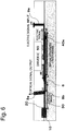
- the placement of the semiconductor laser 1 is determined in such a manner that the semiconductor laser 1 is placed to avoid the electric I/O array 90 and the electrical connecting wires (it is placed on a corner part of the plane in each of Figs. 1 and 2 ).
- the number of channels is increased for the purposes of further downsizing and densification, arrangement of electric wiring will become difficult.
- the semiconductor laser since the semiconductor laser is to be avoided when electric wiring is carried out, it may be necessary to bend an electric wiring line to have a bend angle of 90 degrees or more with respect to the propagation direction of electricity within the driver IC; so that deterioration of an electric signal cannot be avoided, as the speed of a signal for each channel increases. Still further, in the case that the semiconductor laser is placed on the corner part of the plane on the opto-electric hybrid board, and coupled to the optical modulator by use of the optical wave guide with the shortest distance therebetween, there is a problem such that, regarding the optical waveguides 5 arranged between the semiconductor laser 1 and the optical modulator array 60, their line lengths are largely different between respective channels.
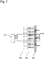
- the semiconductor laser is placed on an output side of the optical modulators, i.e., it is placed near the optical signal outputting parts, in the optical integrated circuit; so that electric wire connection of electrical signal wiring lines, that is highly dependent on frequencies, can be carried out more effectively and freely.
- load on the electric wiring for high-speed/high-frequency use can be reduced.
- an optical pin as an optical interface, deterioration of the above explained electrical wiring can be suppressed, and low-loss coupling to an external waveguide such as a fiber or the like can be carried out without having effect due to placement of the semiconductor laser and/or the driver IC.
- the arrangement of the respective optical elements i.e., the arrangement of the semiconductor laser 10 placed on the side of the optical signal outputting array 80 and the optical couplers 4 (optical branching parts 40a) placed on the side of the electrical I/O array 90 (not shown in the drawing), for the optical transmitter according to an embodiment of the present invention will be further explained in detail.
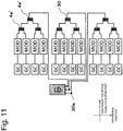
- the optical waveguide PATH[k] arranged between specified adjacent optical modulators is placed in such a manner that it is arranged to couple to the optical coupler MMI[k] through one of the space between the optical modulator MOD[k-1][n] coupled to the optical coupler MMI[k-1] and the optical modulator MOD[k][1] coupled to the optical coupler MMI[k] (the solid line), and the space between the optical modulator MOD[k][n] coupled to the optical coupler MMI[k] and the optical modulator MOD[k+1][1] coupled to the optical coupler MMI[k+1] (the broken line).
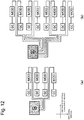
- the optical output comprises 12 channels for the 3-channel semiconductor laser (LD); thus, the 12 optical modulators are divided into groups, each comprising 4 optical modulators; and one optical waveguide 30 or two optical waveguides 30 is/are arranged between adjacent optical modulators between the groups, based on Fig. 7 . Further, by constructing optical branching parts 40a to comprise two-stage arrangement comprising 2-branch-type optical couplers 4a', the laser light outputted from each channel is divided into 4 pieces of input light.
- a reason to construct the optical elements as explained above is to prevent harmful influences on the optical integrated circuit and other elements and devices, due to stray light that is generated when end surfaces of the semiconductor laser and the spot size converter are coupled, confined within the clad, and reflected within the clad and thus guided to propagate therethrough.
Landscapes
- Physics & Mathematics (AREA)
- General Physics & Mathematics (AREA)
- Optics & Photonics (AREA)
- Condensed Matter Physics & Semiconductors (AREA)
- Electromagnetism (AREA)
- Nonlinear Science (AREA)
- Engineering & Computer Science (AREA)
- Microelectronics & Electronic Packaging (AREA)
- Optical Integrated Circuits (AREA)
- Optical Modulation, Optical Deflection, Nonlinear Optics, Optical Demodulation, Optical Logic Elements (AREA)
- Semiconductor Lasers (AREA)
Claims (4)
- Optischer Sender, der auf einer optoelektrischen Hybridplatte bereitgestellt ist, umfassend:einen Halbleiterlaser (10) zum Emittieren von Laserlicht durch Verwendung von mehreren Kanälen; optische Wellenleiter (30), die jeweilig und optisch mit dem Halbleiterlaser (10) gekoppelt sind, um es Teilen des Laserlichts für die jeweiligen Kanäle zu erlauben, sich als Teile von Eingabelicht durch die optischen Wellenleiter (30) auszubreiten; optische Modulatoren (6) zum Erzeugen von optischen Signalen durch Modulieren der Teile des Eingabelichts; optische Signalausgabeabschnitte (80a), jeweilig mit den optischen Modulatoren (6) gekoppelt, zum Ausgeben der durch die optischen Modulatoren (6) ausgebreiteten optischen Signale nach außen; und optische Verzweigungseinheiten (40a), wobei jede der optischen Verzweigungseinheiten (40a) das Laserlicht in zwei oder mehr Teile von Eingabelicht aufteilt, und die Modulatoren (6) jeweilig mit zwei oder mehr optischen Ausgabeanschlüssen, die der optischen Verzweigungseinheit (40a) bereitgestellt sind, gekoppelt sind,wobei auf einer Ebene der optoelektrischen Hybridplatte der Halbleiterlaser (10) auf einer Seite der optischen Signalausgabeabschnitte (80a) gegenüber einer anderen Seite der optischen Signalausgabeabschnitte (80a), wo die optischen Modulatoren (6) platziert sind, platziert ist,dadurch gekennzeichnet, dass dieoptischen Verzweigungseinheiten (40a) auf einer Seite der optischen Modulatoren (6) gegenüber einer anderen Seite der optischen Modulatoren (6), wo der Halbleiterlaser (10) platziert ist, platziert sind.
- Optischer Sender nach Anspruch 1, wobei er dadurch gekennzeichnet ist, dass jeder der optischen Signalausgabeabschnitte (80a) einen Gitterkoppler (8b) zur Beugung des ausgebreiteten optischen Signals und einen optischen Stift (8a) umfasst, der optisch mit dem Gitterkoppler gekoppelt ist und installiert ist, um in einem gewünschten Winkel in Bezug auf eine Ebene der optoelektrischen Hybridplatte zu stehen zum Ausgeben des optischen Signals nach außen.
- Optischer Sender nach Anspruch 1, wobei er dadurch gekennzeichnet ist, dass
der Halbleiterlaser (10) m Kanäle umfasst, wobei m eine Ganzzahl ist, die gleich oder größer als 1 ist, die optischen Wellenleiter (30) erste bis m-te optische Wellenleiter (30) umfassen, und die optischen Verzweigungseinheiten (40a) erste bis m-te optische Verzweigungseinheiten (40a) umfassen,
jede der ersten bis m-ten optischen Verzweigungseinheiten (40a) das Laserlicht in n Teile von Eingabelicht aufteilt, wobei n eine beliebige Ganzzahl ist, die gleich oder größer als 2 ist, und die n Teile von Eingabelicht über die optischen Ausgabeanschlüsse mit ersten bis n-ten optischen Modulatoren (6) gekoppelt sind, und
ein k-ter optischer Wellenleiter (30), wobei k eine beliebige Ganzzahl ist, die gleich 1 oder m ist, oder zwischen 1 und m, gekoppelt ist mit einer k-ten optischen Verzweigungseinheit (40a) durch einen Raum zwischen einem n-ten optischen Modulator (6), der mit einer (k-1)ten optischen Verzweigungseinheit (40a) gekoppelt ist, und einem ersten optischen Modulator (6), der mit der k-ten optischen Verzweigungseinheit (40a) gekoppelt ist, oder einem Raum zwischen einem n-ten optischen Modulator (6), der mit der k-ten optischen Verzweigungseinheit (40a) gekoppelt ist, und einem ersten optischen Modulator (6), der mit einer (k+1)ten optischen Verzweigungseinheit (40a) gekoppelt ist, um die Verbindungslänge von jeder der mehreren optischen Wellenleiter (30) gleich zu machen. - Optischer Sender nach Anspruch 1 oder 3, wobei er dadurch gekennzeichnet ist, dass jede der optischen Verzweigungseinheiten (40a) mehrere zweizweigige optische Koppler (4a') oder mehrere dreizweigige optische Koppler (4a") umfasst, die in mehrfachen Stufen angeordnet sind, um das Laserlicht in eine beliebige Anzahl von Teilen von Eingabelicht aufzuteilen.
Applications Claiming Priority (2)
| Application Number | Priority Date | Filing Date | Title |
|---|---|---|---|
| JP2013151491 | 2013-07-22 | ||
| PCT/JP2014/069164 WO2015012213A1 (ja) | 2013-07-22 | 2014-07-18 | 光電気混載基板に設けた光送信機または光送受信機の送信部 |
Publications (3)
| Publication Number | Publication Date |
|---|---|
| EP3026472A1 EP3026472A1 (de) | 2016-06-01 |
| EP3026472A4 EP3026472A4 (de) | 2017-03-22 |
| EP3026472B1 true EP3026472B1 (de) | 2019-04-10 |
Family
ID=52393254
Family Applications (1)
| Application Number | Title | Priority Date | Filing Date |
|---|---|---|---|
| EP14829257.6A Active EP3026472B1 (de) | 2013-07-22 | 2014-07-18 | Optischer sender für optoelektrische hybridplatte |
Country Status (4)
| Country | Link |
|---|---|
| US (1) | US9577407B2 (de) |
| EP (1) | EP3026472B1 (de) |
| JP (1) | JP6532403B2 (de) |
| WO (1) | WO2015012213A1 (de) |
Families Citing this family (7)
| Publication number | Priority date | Publication date | Assignee | Title |
|---|---|---|---|---|
| US9612401B2 (en) | 2015-02-18 | 2017-04-04 | Ciena Corporation | Method and system for providing optical connections |
| CN105319658A (zh) * | 2015-11-13 | 2016-02-10 | 宁波环球广电科技有限公司 | 一种多通道并行的光收发器件 |
| JP6183527B1 (ja) * | 2016-09-30 | 2017-08-23 | 富士通オプティカルコンポーネンツ株式会社 | 光モジュール及び光変調器 |
| US10527854B1 (en) * | 2018-06-18 | 2020-01-07 | Facebook Technologies, Llc | Illumination source for a waveguide display |
| US12253716B1 (en) * | 2019-10-15 | 2025-03-18 | Acacia Communications, Inc. | Photonic circuits with selectable number of input ports |
| JP2022080627A (ja) | 2020-11-18 | 2022-05-30 | アイオーコア株式会社 | 光モジュール |
| JP2022115723A (ja) | 2021-01-28 | 2022-08-09 | アイオーコア株式会社 | 光電気モジュール |
Family Cites Families (13)
| Publication number | Priority date | Publication date | Assignee | Title |
|---|---|---|---|---|
| JPS62206996A (ja) * | 1986-03-07 | 1987-09-11 | Hitachi Ltd | 光交換方法およびその装置 |
| US5835646A (en) * | 1995-09-19 | 1998-11-10 | Fujitsu Limited | Active optical circuit sheet or active optical circuit board, active optical connector and optical MCM, process for fabricating optical waveguide, and devices obtained thereby |
| DE10112274B4 (de) * | 2001-03-14 | 2006-05-24 | Finisar Corp.(N.D.Ges.D.Staates Delaware), Sunnyvale | Optoelektonisches Sendemodul und Verfahren zu dessen Herstellung |
| US6912333B2 (en) * | 2002-06-21 | 2005-06-28 | Fujitsu Limited | Optical interconnection apparatus and interconnection module |
| JP2005266623A (ja) * | 2004-03-22 | 2005-09-29 | Tokai Univ | 光プリント基板 |
| US20060210215A1 (en) * | 2005-03-15 | 2006-09-21 | Shigenori Aoki | Optical transceiver array |
| WO2007013128A1 (ja) * | 2005-07-25 | 2007-02-01 | Fujitsu Limited | 半導体チップモジュール |
| US7940828B2 (en) * | 2006-02-24 | 2011-05-10 | Nec Corporation | Optical communication system and optical transmitter |
| JP5710499B2 (ja) * | 2009-01-09 | 2015-04-30 | ヒューレット−パッカード デベロップメント カンパニー エル.ピー.Hewlett‐Packard Development Company, L.P. | ポイントツーポイント通信用の光学エンジン |
| US8515217B2 (en) * | 2009-09-02 | 2013-08-20 | Alcatel Lucent | Vertical optically emitting photonic devices with electronic steering capability |
| JP5467826B2 (ja) * | 2009-09-16 | 2014-04-09 | 日東電工株式会社 | 光電気混載モジュールおよびその製造方法 |
| JP2011085647A (ja) * | 2009-10-13 | 2011-04-28 | Hitachi Chem Co Ltd | 光導波路基板及びその製造方法 |
| KR101845514B1 (ko) * | 2010-12-17 | 2018-04-04 | 삼성전자주식회사 | 소형 광 변조기 및 이를 포함하는 광 송신기 |
-
2014
- 2014-07-18 EP EP14829257.6A patent/EP3026472B1/de active Active
- 2014-07-18 JP JP2015528267A patent/JP6532403B2/ja active Active
- 2014-07-18 WO PCT/JP2014/069164 patent/WO2015012213A1/ja not_active Ceased
- 2014-07-18 US US14/906,880 patent/US9577407B2/en active Active
Non-Patent Citations (1)
| Title |
|---|
| None * |
Also Published As
| Publication number | Publication date |
|---|---|
| EP3026472A1 (de) | 2016-06-01 |
| EP3026472A4 (de) | 2017-03-22 |
| US9577407B2 (en) | 2017-02-21 |
| WO2015012213A1 (ja) | 2015-01-29 |
| JPWO2015012213A1 (ja) | 2017-03-02 |
| US20160164251A1 (en) | 2016-06-09 |
| JP6532403B2 (ja) | 2019-06-19 |
Similar Documents
| Publication | Publication Date | Title |
|---|---|---|
| EP3026472B1 (de) | Optischer sender für optoelektrische hybridplatte | |
| KR102009979B1 (ko) | 반도체 패키지 및 이를 포함하는 반도체 장치 | |
| US7536066B2 (en) | Semiconductor chip module | |
| CN116964501A (zh) | 用于将光模块共同封装在开关封装基板上的方法 | |
| CN103814314A (zh) | 光模块 | |
| CN218213537U (zh) | 多通道光收发组件及光模块 | |
| CN110830119B (zh) | 一种光模块 | |
| US20170123173A1 (en) | Optical Integrated Circuit Package | |
| JP2006030868A (ja) | 光電気複合型コネクタ及びそれを用いた基板 | |
| CN207851359U (zh) | 光模块、光模块笼子、光模块组件及光模块系统 | |
| US8363989B2 (en) | Semiconductor optical interconnection device and semiconductor optical interconnection method | |
| US20190361173A1 (en) | Semiconductor device | |
| JP2010225991A (ja) | 多波長レーザ装置 | |
| JP2009104064A (ja) | 光配線を備えた電子装置及びその光配線 | |
| JP2005091460A (ja) | 双方向光モジュール、光送受信装置及び光伝送システム | |
| JP7569441B2 (ja) | 光送受信装置及びそれを用いた光通信装置 | |
| JP6542668B2 (ja) | 光電気混載基板に設けた光送信機または光送受信機の送信部 | |
| CN114594554A (zh) | 一种光模块 | |
| EP4521145A1 (de) | Photonischer integrierter schaltungschip | |
| CN219915983U (zh) | 光学器件 | |
| CN104025376B (zh) | 传输线和传输方法 | |
| CN102957480B (zh) | 光发射装置 | |
| Lee et al. | Increasing bandwidth density in future optical interconnects | |
| KR101265754B1 (ko) | 광 도파로 장치 | |
| WO2005096052A1 (ja) | 光波回路モジュール |
Legal Events
| Date | Code | Title | Description |
|---|---|---|---|
| PUAI | Public reference made under article 153(3) epc to a published international application that has entered the european phase |
Free format text: ORIGINAL CODE: 0009012 |
|
| 17P | Request for examination filed |
Effective date: 20160121 |
|
| AK | Designated contracting states |
Kind code of ref document: A1 Designated state(s): AL AT BE BG CH CY CZ DE DK EE ES FI FR GB GR HR HU IE IS IT LI LT LU LV MC MK MT NL NO PL PT RO RS SE SI SK SM TR |
|
| AX | Request for extension of the european patent |
Extension state: BA ME |
|
| DAX | Request for extension of the european patent (deleted) | ||
| A4 | Supplementary search report drawn up and despatched |
Effective date: 20170221 |
|
| RIC1 | Information provided on ipc code assigned before grant |
Ipc: G02B 6/122 20060101AFI20170215BHEP Ipc: H01S 5/022 20060101ALI20170215BHEP Ipc: G02B 6/28 20060101ALI20170215BHEP Ipc: H01S 5/026 20060101ALI20170215BHEP Ipc: G02B 6/42 20060101ALI20170215BHEP |
|
| RAP1 | Party data changed (applicant data changed or rights of an application transferred) |
Owner name: AIO CORE CO., LTD. |
|
| STAA | Information on the status of an ep patent application or granted ep patent |
Free format text: STATUS: EXAMINATION IS IN PROGRESS |
|
| 17Q | First examination report despatched |
Effective date: 20180905 |
|
| GRAP | Despatch of communication of intention to grant a patent |
Free format text: ORIGINAL CODE: EPIDOSNIGR1 |
|
| STAA | Information on the status of an ep patent application or granted ep patent |
Free format text: STATUS: GRANT OF PATENT IS INTENDED |
|
| INTG | Intention to grant announced |
Effective date: 20181218 |
|
| GRAS | Grant fee paid |
Free format text: ORIGINAL CODE: EPIDOSNIGR3 |
|
| GRAA | (expected) grant |
Free format text: ORIGINAL CODE: 0009210 |
|
| STAA | Information on the status of an ep patent application or granted ep patent |
Free format text: STATUS: THE PATENT HAS BEEN GRANTED |
|
| RAP1 | Party data changed (applicant data changed or rights of an application transferred) |
Owner name: AIO CORE CO., LTD. |
|
| AK | Designated contracting states |
Kind code of ref document: B1 Designated state(s): AL AT BE BG CH CY CZ DE DK EE ES FI FR GB GR HR HU IE IS IT LI LT LU LV MC MK MT NL NO PL PT RO RS SE SI SK SM TR |
|
| REG | Reference to a national code |
Ref country code: GB Ref legal event code: FG4D |
|
| REG | Reference to a national code |
Ref country code: CH Ref legal event code: EP Ref country code: AT Ref legal event code: REF Ref document number: 1119490 Country of ref document: AT Kind code of ref document: T Effective date: 20190415 |
|
| REG | Reference to a national code |
Ref country code: IE Ref legal event code: FG4D |
|
| REG | Reference to a national code |
Ref country code: DE Ref legal event code: R096 Ref document number: 602014044609 Country of ref document: DE |
|
| REG | Reference to a national code |
Ref country code: NL Ref legal event code: MP Effective date: 20190410 |
|
| REG | Reference to a national code |
Ref country code: LT Ref legal event code: MG4D |
|
| REG | Reference to a national code |
Ref country code: AT Ref legal event code: MK05 Ref document number: 1119490 Country of ref document: AT Kind code of ref document: T Effective date: 20190410 |
|
| PG25 | Lapsed in a contracting state [announced via postgrant information from national office to epo] |
Ref country code: NL Free format text: LAPSE BECAUSE OF FAILURE TO SUBMIT A TRANSLATION OF THE DESCRIPTION OR TO PAY THE FEE WITHIN THE PRESCRIBED TIME-LIMIT Effective date: 20190410 |
|
| PG25 | Lapsed in a contracting state [announced via postgrant information from national office to epo] |
Ref country code: HR Free format text: LAPSE BECAUSE OF FAILURE TO SUBMIT A TRANSLATION OF THE DESCRIPTION OR TO PAY THE FEE WITHIN THE PRESCRIBED TIME-LIMIT Effective date: 20190410 Ref country code: LT Free format text: LAPSE BECAUSE OF FAILURE TO SUBMIT A TRANSLATION OF THE DESCRIPTION OR TO PAY THE FEE WITHIN THE PRESCRIBED TIME-LIMIT Effective date: 20190410 Ref country code: PT Free format text: LAPSE BECAUSE OF FAILURE TO SUBMIT A TRANSLATION OF THE DESCRIPTION OR TO PAY THE FEE WITHIN THE PRESCRIBED TIME-LIMIT Effective date: 20190910 Ref country code: SE Free format text: LAPSE BECAUSE OF FAILURE TO SUBMIT A TRANSLATION OF THE DESCRIPTION OR TO PAY THE FEE WITHIN THE PRESCRIBED TIME-LIMIT Effective date: 20190410 Ref country code: FI Free format text: LAPSE BECAUSE OF FAILURE TO SUBMIT A TRANSLATION OF THE DESCRIPTION OR TO PAY THE FEE WITHIN THE PRESCRIBED TIME-LIMIT Effective date: 20190410 Ref country code: AL Free format text: LAPSE BECAUSE OF FAILURE TO SUBMIT A TRANSLATION OF THE DESCRIPTION OR TO PAY THE FEE WITHIN THE PRESCRIBED TIME-LIMIT Effective date: 20190410 Ref country code: ES Free format text: LAPSE BECAUSE OF FAILURE TO SUBMIT A TRANSLATION OF THE DESCRIPTION OR TO PAY THE FEE WITHIN THE PRESCRIBED TIME-LIMIT Effective date: 20190410 Ref country code: NO Free format text: LAPSE BECAUSE OF FAILURE TO SUBMIT A TRANSLATION OF THE DESCRIPTION OR TO PAY THE FEE WITHIN THE PRESCRIBED TIME-LIMIT Effective date: 20190710 |
|
| PG25 | Lapsed in a contracting state [announced via postgrant information from national office to epo] |
Ref country code: BG Free format text: LAPSE BECAUSE OF FAILURE TO SUBMIT A TRANSLATION OF THE DESCRIPTION OR TO PAY THE FEE WITHIN THE PRESCRIBED TIME-LIMIT Effective date: 20190710 Ref country code: GR Free format text: LAPSE BECAUSE OF FAILURE TO SUBMIT A TRANSLATION OF THE DESCRIPTION OR TO PAY THE FEE WITHIN THE PRESCRIBED TIME-LIMIT Effective date: 20190711 Ref country code: PL Free format text: LAPSE BECAUSE OF FAILURE TO SUBMIT A TRANSLATION OF THE DESCRIPTION OR TO PAY THE FEE WITHIN THE PRESCRIBED TIME-LIMIT Effective date: 20190410 Ref country code: RS Free format text: LAPSE BECAUSE OF FAILURE TO SUBMIT A TRANSLATION OF THE DESCRIPTION OR TO PAY THE FEE WITHIN THE PRESCRIBED TIME-LIMIT Effective date: 20190410 Ref country code: LV Free format text: LAPSE BECAUSE OF FAILURE TO SUBMIT A TRANSLATION OF THE DESCRIPTION OR TO PAY THE FEE WITHIN THE PRESCRIBED TIME-LIMIT Effective date: 20190410 |
|
| PG25 | Lapsed in a contracting state [announced via postgrant information from national office to epo] |
Ref country code: AT Free format text: LAPSE BECAUSE OF FAILURE TO SUBMIT A TRANSLATION OF THE DESCRIPTION OR TO PAY THE FEE WITHIN THE PRESCRIBED TIME-LIMIT Effective date: 20190410 Ref country code: IS Free format text: LAPSE BECAUSE OF FAILURE TO SUBMIT A TRANSLATION OF THE DESCRIPTION OR TO PAY THE FEE WITHIN THE PRESCRIBED TIME-LIMIT Effective date: 20190810 |
|
| REG | Reference to a national code |
Ref country code: DE Ref legal event code: R097 Ref document number: 602014044609 Country of ref document: DE |
|
| PG25 | Lapsed in a contracting state [announced via postgrant information from national office to epo] |
Ref country code: EE Free format text: LAPSE BECAUSE OF FAILURE TO SUBMIT A TRANSLATION OF THE DESCRIPTION OR TO PAY THE FEE WITHIN THE PRESCRIBED TIME-LIMIT Effective date: 20190410 Ref country code: DK Free format text: LAPSE BECAUSE OF FAILURE TO SUBMIT A TRANSLATION OF THE DESCRIPTION OR TO PAY THE FEE WITHIN THE PRESCRIBED TIME-LIMIT Effective date: 20190410 Ref country code: RO Free format text: LAPSE BECAUSE OF FAILURE TO SUBMIT A TRANSLATION OF THE DESCRIPTION OR TO PAY THE FEE WITHIN THE PRESCRIBED TIME-LIMIT Effective date: 20190410 Ref country code: CZ Free format text: LAPSE BECAUSE OF FAILURE TO SUBMIT A TRANSLATION OF THE DESCRIPTION OR TO PAY THE FEE WITHIN THE PRESCRIBED TIME-LIMIT Effective date: 20190410 Ref country code: SK Free format text: LAPSE BECAUSE OF FAILURE TO SUBMIT A TRANSLATION OF THE DESCRIPTION OR TO PAY THE FEE WITHIN THE PRESCRIBED TIME-LIMIT Effective date: 20190410 |
|
| PLBE | No opposition filed within time limit |
Free format text: ORIGINAL CODE: 0009261 |
|
| STAA | Information on the status of an ep patent application or granted ep patent |
Free format text: STATUS: NO OPPOSITION FILED WITHIN TIME LIMIT |
|
| PG25 | Lapsed in a contracting state [announced via postgrant information from national office to epo] |
Ref country code: IT Free format text: LAPSE BECAUSE OF FAILURE TO SUBMIT A TRANSLATION OF THE DESCRIPTION OR TO PAY THE FEE WITHIN THE PRESCRIBED TIME-LIMIT Effective date: 20190410 Ref country code: SM Free format text: LAPSE BECAUSE OF FAILURE TO SUBMIT A TRANSLATION OF THE DESCRIPTION OR TO PAY THE FEE WITHIN THE PRESCRIBED TIME-LIMIT Effective date: 20190410 Ref country code: MC Free format text: LAPSE BECAUSE OF FAILURE TO SUBMIT A TRANSLATION OF THE DESCRIPTION OR TO PAY THE FEE WITHIN THE PRESCRIBED TIME-LIMIT Effective date: 20190410 |
|
| REG | Reference to a national code |
Ref country code: CH Ref legal event code: PL |
|
| 26N | No opposition filed |
Effective date: 20200113 |
|
| PG25 | Lapsed in a contracting state [announced via postgrant information from national office to epo] |
Ref country code: TR Free format text: LAPSE BECAUSE OF FAILURE TO SUBMIT A TRANSLATION OF THE DESCRIPTION OR TO PAY THE FEE WITHIN THE PRESCRIBED TIME-LIMIT Effective date: 20190410 |
|
| REG | Reference to a national code |
Ref country code: BE Ref legal event code: MM Effective date: 20190731 |
|
| PG25 | Lapsed in a contracting state [announced via postgrant information from national office to epo] |
Ref country code: BE Free format text: LAPSE BECAUSE OF NON-PAYMENT OF DUE FEES Effective date: 20190731 Ref country code: LU Free format text: LAPSE BECAUSE OF NON-PAYMENT OF DUE FEES Effective date: 20190718 Ref country code: CH Free format text: LAPSE BECAUSE OF NON-PAYMENT OF DUE FEES Effective date: 20190731 Ref country code: SI Free format text: LAPSE BECAUSE OF FAILURE TO SUBMIT A TRANSLATION OF THE DESCRIPTION OR TO PAY THE FEE WITHIN THE PRESCRIBED TIME-LIMIT Effective date: 20190410 Ref country code: LI Free format text: LAPSE BECAUSE OF NON-PAYMENT OF DUE FEES Effective date: 20190731 |
|
| PG25 | Lapsed in a contracting state [announced via postgrant information from national office to epo] |
Ref country code: IE Free format text: LAPSE BECAUSE OF NON-PAYMENT OF DUE FEES Effective date: 20190718 |
|
| PG25 | Lapsed in a contracting state [announced via postgrant information from national office to epo] |
Ref country code: CY Free format text: LAPSE BECAUSE OF FAILURE TO SUBMIT A TRANSLATION OF THE DESCRIPTION OR TO PAY THE FEE WITHIN THE PRESCRIBED TIME-LIMIT Effective date: 20190410 |
|
| PG25 | Lapsed in a contracting state [announced via postgrant information from national office to epo] |
Ref country code: MT Free format text: LAPSE BECAUSE OF FAILURE TO SUBMIT A TRANSLATION OF THE DESCRIPTION OR TO PAY THE FEE WITHIN THE PRESCRIBED TIME-LIMIT Effective date: 20190410 Ref country code: HU Free format text: LAPSE BECAUSE OF FAILURE TO SUBMIT A TRANSLATION OF THE DESCRIPTION OR TO PAY THE FEE WITHIN THE PRESCRIBED TIME-LIMIT; INVALID AB INITIO Effective date: 20140718 |
|
| PG25 | Lapsed in a contracting state [announced via postgrant information from national office to epo] |
Ref country code: MK Free format text: LAPSE BECAUSE OF FAILURE TO SUBMIT A TRANSLATION OF THE DESCRIPTION OR TO PAY THE FEE WITHIN THE PRESCRIBED TIME-LIMIT Effective date: 20190410 |
|
| PGFP | Annual fee paid to national office [announced via postgrant information from national office to epo] |
Ref country code: GB Payment date: 20250527 Year of fee payment: 12 |
|
| PGFP | Annual fee paid to national office [announced via postgrant information from national office to epo] |
Ref country code: FR Payment date: 20250519 Year of fee payment: 12 |
|
| PGFP | Annual fee paid to national office [announced via postgrant information from national office to epo] |
Ref country code: DE Payment date: 20250728 Year of fee payment: 12 |