EP3121858A1 - Halbleiterchip und verfahren zur herstellung eines halbleiterchips - Google Patents
Halbleiterchip und verfahren zur herstellung eines halbleiterchips Download PDFInfo
- Publication number
- EP3121858A1 EP3121858A1 EP16187689.1A EP16187689A EP3121858A1 EP 3121858 A1 EP3121858 A1 EP 3121858A1 EP 16187689 A EP16187689 A EP 16187689A EP 3121858 A1 EP3121858 A1 EP 3121858A1
- Authority
- EP
- European Patent Office
- Prior art keywords
- layer
- contact
- semiconductor
- semiconductor chip
- active region
- Prior art date
- Legal status (The legal status is an assumption and is not a legal conclusion. Google has not performed a legal analysis and makes no representation as to the accuracy of the status listed.)
- Withdrawn
Links
Images


Classifications
-
- H—ELECTRICITY
- H10—SEMICONDUCTOR DEVICES; ELECTRIC SOLID-STATE DEVICES NOT OTHERWISE PROVIDED FOR
- H10H—INORGANIC LIGHT-EMITTING SEMICONDUCTOR DEVICES HAVING POTENTIAL BARRIERS
- H10H20/00—Individual inorganic light-emitting semiconductor devices having potential barriers, e.g. light-emitting diodes [LED]
- H10H20/80—Constructional details
- H10H20/81—Bodies
- H10H20/816—Bodies having carrier transport control structures, e.g. highly-doped semiconductor layers or current-blocking structures
- H10H20/8162—Current-blocking structures
-
- H—ELECTRICITY
- H10—SEMICONDUCTOR DEVICES; ELECTRIC SOLID-STATE DEVICES NOT OTHERWISE PROVIDED FOR
- H10H—INORGANIC LIGHT-EMITTING SEMICONDUCTOR DEVICES HAVING POTENTIAL BARRIERS
- H10H20/00—Individual inorganic light-emitting semiconductor devices having potential barriers, e.g. light-emitting diodes [LED]
- H10H20/80—Constructional details
- H10H20/81—Bodies
- H10H20/811—Bodies having quantum effect structures or superlattices, e.g. tunnel junctions
-
- H—ELECTRICITY
- H01—ELECTRIC ELEMENTS
- H01L—SEMICONDUCTOR DEVICES NOT COVERED BY CLASS H10
- H01L2924/00—Indexing scheme for arrangements or methods for connecting or disconnecting semiconductor or solid-state bodies as covered by H01L24/00
- H01L2924/0001—Technical content checked by a classifier
- H01L2924/0002—Not covered by any one of groups H01L24/00, H01L24/00 and H01L2224/00
-
- H—ELECTRICITY
- H10—SEMICONDUCTOR DEVICES; ELECTRIC SOLID-STATE DEVICES NOT OTHERWISE PROVIDED FOR
- H10H—INORGANIC LIGHT-EMITTING SEMICONDUCTOR DEVICES HAVING POTENTIAL BARRIERS
- H10H20/00—Individual inorganic light-emitting semiconductor devices having potential barriers, e.g. light-emitting diodes [LED]
- H10H20/80—Constructional details
- H10H20/83—Electrodes
- H10H20/831—Electrodes characterised by their shape
- H10H20/8314—Electrodes characterised by their shape extending at least partially onto an outer side surface of the bodies
-
- H—ELECTRICITY
- H10—SEMICONDUCTOR DEVICES; ELECTRIC SOLID-STATE DEVICES NOT OTHERWISE PROVIDED FOR
- H10H—INORGANIC LIGHT-EMITTING SEMICONDUCTOR DEVICES HAVING POTENTIAL BARRIERS
- H10H20/00—Individual inorganic light-emitting semiconductor devices having potential barriers, e.g. light-emitting diodes [LED]
- H10H20/80—Constructional details
- H10H20/83—Electrodes
- H10H20/831—Electrodes characterised by their shape
- H10H20/8316—Multi-layer electrodes comprising at least one discontinuous layer
-
- H—ELECTRICITY
- H10—SEMICONDUCTOR DEVICES; ELECTRIC SOLID-STATE DEVICES NOT OTHERWISE PROVIDED FOR
- H10H—INORGANIC LIGHT-EMITTING SEMICONDUCTOR DEVICES HAVING POTENTIAL BARRIERS
- H10H20/00—Individual inorganic light-emitting semiconductor devices having potential barriers, e.g. light-emitting diodes [LED]
- H10H20/80—Constructional details
- H10H20/83—Electrodes
- H10H20/832—Electrodes characterised by their material
- H10H20/833—Transparent materials
-
- H—ELECTRICITY
- H10—SEMICONDUCTOR DEVICES; ELECTRIC SOLID-STATE DEVICES NOT OTHERWISE PROVIDED FOR
- H10H—INORGANIC LIGHT-EMITTING SEMICONDUCTOR DEVICES HAVING POTENTIAL BARRIERS
- H10H20/00—Individual inorganic light-emitting semiconductor devices having potential barriers, e.g. light-emitting diodes [LED]
- H10H20/80—Constructional details
- H10H20/83—Electrodes
- H10H20/832—Electrodes characterised by their material
- H10H20/835—Reflective materials
Definitions
- the invention relates to a semiconductor chip and to a method for producing a semiconductor chip.
- the coupling-out efficiency that is to say the ratio of radiation power emerging from the semiconductor to the radiation power generated in the semiconductor chip, is influenced by numerous loss processes.
- absorption losses can be the cause of a reduction in the coupling-out efficiency.
- a semiconductor chip according to the invention comprises a semiconductor body with a semiconductor layer sequence, which includes a semiconductor body for generating Radiation provided active area. On the semiconductor body, a contact is arranged.
- the vertical injection of charge carriers from the contact into the active region is reduced by means of the injection barrier.
- the injection of charge carriers into the active area takes place predominantly in addition to the contact.
- the contact expediently has a smaller lateral extent than the active region. Below the contact, however, the injection of charge carriers into the active area is reduced. In this way, the probability of radiation below the contact being generated in the active region and subsequently being absorbed by the contact can be reduced. In other words, radiation in the active region of the semiconductor chip is generated predominantly in lateral regions in which radiation emitted in the vertical direction is not absorbed by an overlying contact but can emerge from the semiconductor chip. The coupling-out efficiency of the semiconductor chip can thus be increased.
- the injection barrier is adapted in its lateral shape to a lateral shape of the contact.
- the injection barrier can overlap with the contact, preferably completely.
- the injection barrier in supervision preferably has the same basic geometric shape as the contact.
- a lateral direction is understood to mean a direction which extends along a main extension direction of the semiconductor layers of the semiconductor layer sequence. Accordingly, a vertical direction is perpendicular to the main extension direction of these semiconductor layers.
- the injection barrier is formed at an interface between the contact and the semiconductor body.
- the injection barrier can be imaged by means of a potential barrier, in particular by means of a Schottky contact, that is to say a metal-semiconductor junction, between the contact and the semiconductor body.
- the injection barrier can be formed in a recess in the semiconductor body.
- the recess for example, material of the semiconductor body which has a comparatively low contact resistance to the contact may be removed. As a result, material of the semiconductor body may be exposed, which has a higher contact resistance to the contact.
- the contact arranged in the recess can have a higher contact resistance to the semiconductor body in the vertical direction than in the lateral direction. In this way a direct vertical injection of charge carriers from the contact into the active region is reduced.
- a production-related not completely avoidable contact resistance in particular an ohmic contact resistance with a linear or at least approximately linear current-voltage characteristic, between a metal contact and a semiconductor layer not as Injection barrier is considered within the meaning of the present invention.
- the injection barrier is preferably designed such that in the operation of the semiconductor chip by means of an external electrical voltage in the contact impressed charge carriers are not injected in supervision of the semiconductor chip in the injection barrier or at least with a much lower probability in the active area, than outside the injection barrier.
- the injection barrier has a smaller lateral extent than the active area.
- the injection barrier is formed in the semiconductor body.
- the injection barrier is formed by means of a region in which an electrical conductivity of a semiconductor layer arranged between the active region and the contact is locally reduced.
- the conductivity of the semiconductor layer is thus lower in this range than outside this range.
- the conductivity in this region is reduced compared to a laterally adjacent region of the semiconductor layer.
- this region of lower conductivity in the lateral direction is preferably island-like and, in its lateral shape, is particularly preferably adapted to the lateral shape of the contact.
- the region in which the conductivity is reduced may be vertically spaced from the contact.
- charge carriers can be injected directly into the semiconductor body from the contact during operation of the semiconductor chip in the vertical direction. Further direct vertical injection into the active region becomes due to this region of low electrical conductivity prevented or at least reduced in favor of an increased injection outside of this range. The coupling-out efficiency of the semiconductor body can thus be increased.
- the injection barrier is formed outside the semiconductor body.
- the injection barrier is formed by means of an insulating layer, which is arranged between the semiconductor body and the contact.
- a plurality of insulation layers may be formed between the semiconductor body and the contact.
- the plurality of insulating layers are formed according to a Bragg mirror.
- a dielectric mirror is formed by means of the insulating layer.
- the injection barrier can thus additionally fulfill the function of a mirror for radiation generated in the active region. Absorption of this radiation in the contact can be so greatly reduced. The radiation reflected at the injection barrier, in particular at the dielectric mirror, can subsequently emerge from the semiconductor chip. The coupling-out efficiency of the semiconductor chip can thus be increased further.
- the contact has a contact layer which terminates the contact on the side facing away from the semiconductor body.
- the contact layer is used in particular for external contacting of the semiconductor chip, for example by means of a bonding wire.
- the contact layer preferably contains a metal, about Au, Ti, Pt or Ni, or a metallic alloy with at least one of these materials.
- the contact has a mirror layer, which is arranged between the contact layer and the semiconductor body.
- the mirror layer preferably has a high reflectivity for radiation generated in the active region.
- the mirror layer preferably contains a metal, such as gold, aluminum, silver, palladium or rhodium or a metallic alloy containing at least one of said metals.
- the contact layer may protrude beyond the mirror layer at least in regions in the lateral direction.
- the contact layer can overmold the mirror layer in the lateral direction, that is to say the contact layer also covers the mirror layer on at least one side surface. In this way, a direct injection of charge carriers from the contact layer into a laterally adjacent layer to the contact layer can be simplified.
- the mirror layer in this case makes no or at least no significant contribution to the injection of charge carriers from the contact into the semiconductor body.
- the mirror layer can be arranged on the side of the insulating layer or the plurality of insulating layers which faces away from the active region. In this way, radiation transmitted by the insulating layers can be reflected at the mirror layer.
- a mirror composite with high overall reflectivity for radiation generated in the active region can be formed simplified in this way.
- the semiconductor chip has a Stromverbreiterungstik which is electrically connected to the contact.
- the current broadening layer is provided to inject charge carriers into the active region in a top view onto the semiconductor chip outside the injection barrier.
- the current spreading layer preferably has a large lateral extent compared to the contact.
- the current broadening layer adjoins a side surface of the semiconductor body which delimits the active region in a lateral direction. A large-scale impression of charge carriers in the active area is thereby simplified.
- the Stromverbreiterungs Mrs has a recess in which the contact is arranged.
- the recess may also extend in the vertical direction through the current broadening layer. Vertical injection of charge carriers from the contact into the current spreading layer can thus be reduced.
- the current broadening layer and the contact can in this case adjoin one another at least in regions in the lateral direction. Charge carriers can thus be injected in the lateral direction directly from the contact into the current broadening layer.
- the current spreading layer and the contact may be laterally spaced apart.
- the current spreading layer and the contact are preferably electrically connected by means of a layer which is arranged between the contact and the active region.
- the current broadening layer is non-metallic.
- the current broadening layer is preferably formed by means of a material which is permeable to the radiation generated in the active region.
- the current distribution layer may therefore be non-metallic and permeable to radiation generated in the active region.
- a non-metallic current broadening layer is understood as meaning a layer or layer sequence, wherein the layer or the individual layers of the layer sequence may indeed contain a metal but have no metallic properties.
- the non-metallic current spreading layer may be based on semiconductor material or consist of semiconductor material.
- the current broadening layer can thus be formed in the semiconductor body.
- the current spreading layer is preferably a semiconductor layer different in conduction type from another semiconductor layer disposed between the semiconductor layer and the active region.
- the current broadening layer may be arranged outside the semiconductor body.
- the semiconductor body Preferably contains one outside the semiconductor body arranged Stromverbreiterungstik a TCO material (transparent conductive oxide).
- TCO materials are transparent, conductive oxides, usually metal oxides, such as zinc oxide, tin oxide, cadmium oxide, titanium oxide, indium oxide or indium tin oxide (ITO).
- metal oxides such as zinc oxide, tin oxide, cadmium oxide, titanium oxide, indium oxide or indium tin oxide (ITO).
- binary metal oxygen compounds such as ZnO, SnO 2 or In 2 O 3 also include ternary metal oxygen compounds such as Zn 2 SnO 4 , CdSnO 3 , ZnSnO 3 , MgIn 2 O 4 , GaInO 3 , Zn 2 In 2 O 5 or In 4 Sn 3 O 12 or mixtures of different transparent conductive oxides to the group of TCOs.
- the TCOs do not necessarily correspond to a stoichiometric composition and may also be p- or n-doped.
- connection layer is arranged between the current broadening layer and the semiconductor body.
- the connection layer expediently contains a material with which an electrically conductive connection to a semiconductor layer with low contact resistance can be produced.
- the terminal layer contains a metal, such as titanium, platinum, nickel, rhodium or a metallic alloy with at least one of said materials.
- the connection layer is made sufficiently thin, so that it is at least partially transparent for radiation generated in the active region.
- the thickness of the connection layer is at most 10 nm.
- a tunnel contact layer is arranged between the current broadening layer and the active region.
- the tunnel contact layer is different in their type of conduction from another semiconductor layer disposed between the tunnel contact layer and the active region.
- the tunnel contact layer is preferably a highly doped semiconductor layer.
- the doping concentration is preferably at least 10 18 cm -3 , more preferably at least 10 19 cm -3 .
- the tunnel contact layer By means of the tunnel contact layer, the injection of charge carriers from the current spreading layer into the active region can be simplified.
- a further tunnel contact layer is arranged on the side of the tunnel contact layer facing the active region.
- the further tunnel contact layer has a different conductivity type than the tunnel contact layer.
- the further tunnel contact layer preferably also has a high doping concentration.
- the injection barrier is formed by means of a region of the further tunnel contact layer, in which the electrical conductivity is reduced locally.
- the injection barrier is thus formed in the semiconductor body.
- the tunnel contact layer may be formed between the contact and the further tunnel contact layer.
- the region of locally reduced conductivity can thus be spaced from the contact in the vertical direction.
- charge carriers can thus pass from the contact into the tunnel contact layer and propagate in the lateral direction.
- the spreading of the charge carriers in the lateral direction can continue by means of, within or arranged outside the semiconductor body, current broadening layer to be promoted. From the tunnel contact layer, the charge carriers can subsequently be injected into the active region beyond the region of locally reduced electrical conductivity via the further tunnel contact layer.
- the tunnel contact layer and / or the further tunnel contact layer can be made comparatively thin.
- the thickness may be 100 nm or less, preferably 20 nm or less, more preferably 10 nm or less.
- the current broadening layer is designed as a tunnel contact layer.
- the current broadening layer is thus a highly doped semiconductor layer and thus part of the semiconductor body. Further layers of current distribution arranged outside the semiconductor body and impressions of charge carriers which are uniform in the lateral direction into the active region can be dispensed with in this case.
- a further tunnel contact layer may in turn be arranged, wherein the further tunnel contact layer has a different conductivity type than the tunnel contact layer.
- the semiconductor chip is preferably provided for generating incoherent or predominantly incoherent radiation.
- the semiconductor chip as an LED chip or as a further RCLED chip (resonant cavity be executed light emitting).
- the active region is arranged within a cavity.
- the semiconductor chip can also be provided for generating coherent radiation.
- the semiconductor chip may be embodied as a semiconductor laser chip, in particular as an internal cavity surface emitting semiconductor laser chip (VCSEL) or as a surface emitting semiconductor chip for operation with an external cavity surface emitting laser (VECSEL).
- VCSEL internal cavity surface emitting semiconductor laser chip
- VECSEL external cavity surface emitting laser
- the semiconductor body in particular the active region, preferably contains a III-V semiconductor material.
- III-V semiconductor materials By means of III-V semiconductor materials, radiation from the infrared to the ultraviolet spectral range can be generated with high efficiency.
- the semiconductor chip in particular the semiconductor body, can also have more than one active region, for example two or more active regions arranged one above the other.
- the arrangement of the above-mentioned elements of the semiconductor chip, in particular the current spreading layer, the tunnel contact layer, the further tunnel contact layer and the connection layer relative to the active region refers to the active region which is arranged closest to the contact.
- a contact is made on the semiconductor body applied. Between the active area and the contact an injection barrier is formed.
- the injection barrier is formed in the semiconductor body. This is done in particular before the application of the contact on the semiconductor body.
- the injection barrier is formed in the semiconductor body by means of a region of a semiconductor layer in which the electrical conductivity of the semiconductor layer is locally reduced.
- This local reduction of the electrical conductivity of the semiconductor layer can take place, for example, by compensation of the doping, for example by targeted disruption of the crystal structure. For example, selectively generated crystal defects in an originally p-doped semiconductor layer can lead to complete or at least partial compensation of the p-doping.
- the conditional by the acceptors of the p-type semiconductor layer electrical conductivity is thereby reduced by the impurities that act as a donor. This can be achieved for example by means of back sputtering. In backsputtering, an ion beam, such as an Ar ion beam, is preferably directed onto the semiconductor layer.
- the local reduction of the electrical conductivity can also be achieved by an at least partial deactivation of the donors or acceptors.
- hydrogen can be introduced into the p-conducting semiconductor layer by means of a hydrogen plasma.
- Acceptors such as Mg acceptors in a p-type doped, on InGaAlN based semiconductor layer, so can be electrically disabled.
- the electrical conductivity can be reduced.
- a current broadening layer for example by means of sputtering or vapor deposition, is applied to the semiconductor body.
- a laterally structured masking layer can be formed or arranged on the current spreading layer. Subsequently, in a region free from the masking layer, material of the current spreading layer and the semiconductor body can be removed.
- the lateral structuring of the current broadening layer and of the semiconductor body can therefore be effected by means of a common masking layer.
- An additional masking layer can therefore be dispensed with. As a result, the manufacturing cost can be reduced. Furthermore, the structuring accuracy can be increased thereby.
- a further laterally structured masking layer is formed on the current broadening layer. This is preferably done after removal of the masking layer.
- a recess can be formed in the current broadening layer.
- a mirror layer and subsequently a contact layer can be applied.
- the deposition conditions in the production of the mirror layer and the contact layer can be adjusted such that the contact layer projects laterally beyond the mirror layer.
- the mirror layer can be deposited on the semiconductor body from a vertical or substantially perpendicular direction, while the contact layer is deposited obliquely with simultaneous rotation of the semiconductor body. It can thereby be achieved that the contact layer has a greater lateral extent than the mirror layer, without the need for different masking layers.
- the contact or at least one layer of the contact may be formed in the recess of the current spreading layer such that the contact is laterally spaced from the current spreading layer. This can be done by means of the same further masking layer.
- the recess in the current spreading layer can be formed by wet chemical etching.
- the recess in the current broadening layer can thus assume a greater lateral extent than the recess in the further masking layer.
- the contact or at least one layer of the contact may be deposited so that the lateral extent of the contact or the at least one layer of the contact is less than or equal to the lateral extent of the recess in the further masking layer. This can be done by deposition from vertical or substantially vertical direction. Thus, a gap between the contact or the at least one layer of the contact can be formed.
- the production of the layers arranged on the semiconductor body, in particular the current spreading layer, the contact layer, the mirror layer and the connection layer, preferably takes place by means of vapor deposition or sputtering.
- the method described is particularly suitable for producing a semiconductor chip described above. Therefore, features implemented in connection with the semiconductor chip can also be used for the method and vice versa.
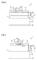
- FIG. 1 A first exemplary embodiment of a semiconductor chip according to the invention is shown in FIG FIG. 1 schematically shown in sectional view.
- the semiconductor chip 1 has a semiconductor body 2 with a semiconductor layer sequence.
- the semiconductor layer sequence forms the semiconductor body.
- the semiconductor body has an active region 23 which is arranged between a p-type semiconductor layer 21 and an n-type semiconductor layer 22.
- the semiconductor body 2 is arranged on a carrier 20.
- the carrier 20 may, for example, be a growth substrate for the semiconductor layer sequence of the semiconductor body 2.
- the carrier may include or may be composed of a semiconductor such as Si, Ge, GaAs, SiC, GaN, or GaP.
- a carrier containing sapphire or made of sapphire application Find may be suitably doped.
- the semiconductor layer sequence of the semiconductor body 2 is preferably epitaxially deposited on the growth substrate, such as by MBE or MOVPE.
- a contact 4 is arranged on the semiconductor body 2 and may, for example, have a circular or rectangular basic shape.
- the contact 4 has a contact layer 41 and a mirror layer 42.
- the mirror layer is arranged between the contact layer and the semiconductor body 2.
- an injection barrier 5 is formed between the contact 4 and the semiconductor body 2.
- the injection barrier is formed at an interface 25 of the semiconductor body 2, which delimits the semiconductor body in the vertical direction on the side facing away from the carrier 20.
- the injection barrier is designed as a Schottky contact between the contact 4 and the semiconductor body 2, in particular as a Schottky contact between the mirror layer 42 and the p-type semiconductor layer 21.
- the lateral extent of the injection barrier 5 corresponds to the lateral extent of the contact 4.
- a current spreading layer 31 is arranged on the semiconductor body 2.
- the current spreading layer 31 is disposed on the same side of the semiconductor body 2 as the contact 4.
- the lateral extent of the current spreading layer is large compared to that of the contact 4.
- the current spreading layer 31 has a recess 310.
- the recess preferably extends in the vertical direction through the current broadening layer 31.
- the contact 4 in particular the contact layer 41, is arranged.
- injected charge carriers can thus pass directly from the contact layer in the Stromverbreiterungs Mrs 31 in the lateral direction.
- the charge carriers can be injected in the vertical direction into the semiconductor body, in particular into the active region 23.
- a direct vertical injection from the contact layer 41 into the semiconductor body 2 is made more difficult by means of the injection barrier 5.
- radiation in the active region is thus generated predominantly outside the injection barrier 5. The coupling-out efficiency of the semiconductor chip 1 can thereby be increased.
- the current broadening layer 31 is preferably non-metallic and is furthermore preferably permeable to radiation generated in the active region.
- the current spreading layer 31 preferably contains a TCO material, for example indium tin oxide (ITO) or zinc oxide (ZnO). Also, a TCO material mentioned above may be suitable for the current spreading layer 31.
- connection layer 32 is formed between the current spreading layer 31 and the semiconductor body 2.
- the connection layer 32 can charge carriers in a simplified manner, the current spreading layer 31 can be injected into the semiconductor body 2.
- the connection layer it is thus also possible to use materials for the current broadening layer with which a low, in particular ohmic, contact resistance to the semiconductor body 2 is difficult or impossible to realize. With a sufficiently good electrical contact between the Stromverumblerungs Mrs 31 and the semiconductor body 2 can be dispensed with the connection layer.
- connection layer 32 is preferably metallic or based on a metallic alloy. Furthermore, the connection layer is preferably made so thin that radiation generated in the active region can at least partially pass through the connection layer.
- the terminal layer may contain, for example, titanium, platinum, nickel, rhodium or another metal with good contact properties to a semiconductor layer.
- the connection layer may contain a metallic alloy, preferably with at least one of said materials. Platinum has been found to be particularly advantageous.
- the thickness of the connection layer is preferably at most 10 nm, for example 3 to 7 nm. For example, a platinum layer with a thickness of 6 nm in the blue spectral range has a transmission of about 40%.
- the injection barrier 5 preferably projects completely beyond the contact 4.
- the injection barrier 5 preferably projects completely beyond the contact 4.
- the mirror layer 42 serves to further reduce absorption in the contact, in particular in the contact layer 41.
- the mirror layer is expediently formed by means of a material which has as high a reflectivity as possible for radiation generated in the active region.
- the mirror layer is metallic or based on a metallic alloy.
- In the infrared and red spectral range for example, gold, in the blue, green and ultraviolet spectral range, aluminum, silver, palladium and rhodium have a relatively high reflectivity.
- the material for the contact layer 41 can therefore be largely independent of the optical properties with respect to a good external Contactability of the semiconductor chip, for example by means of a bonding wire can be selected.
- the material is in particular a metal, such as gold or a metallic alloy containing, for example, gold, such as AuSn.
- a further contact 45 is arranged on the side facing away from the semiconductor body 2 of the carrier 20, a further contact 45 is arranged.
- charge carriers can be injected into the active region and recombined there under emission and radiation.
- the semiconductor body 2, in particular the active region 23, preferably contains a III-V semiconductor material.
- III-V semiconductor materials are used for generating radiation in the ultraviolet (In x Ga y Al 1-xy N) over the visible (In x Ga y Al 1-xy N, in particular for blue to green radiation, or In x Ga y Al 1- xy P, in particular for yellow to red radiation) to the infrared (In x Ga y Al 1-xy As) spectral range is particularly suitable.
- 0 ⁇ x ⁇ 1, 0 ⁇ y ⁇ 1 and x + y ⁇ 1 in particular with x ⁇ 1, y ⁇ 1, x ⁇ 0 and / or y ⁇ 0.
- a protective layer 7 is arranged, which preferably also covers the semiconductor body at its side surfaces.
- This protective layer serves to protect the semiconductor body from harmful external environmental influences, such as moisture.
- a protective layer is not absolutely necessary.
- the protective layer is expediently formed dielectrically and preferably contains an oxide, such as silicon oxide Nitride, such as silicon nitride, or an oxynitride, such as silicon oxynitride.
- the doping of the semiconductor layers is given by way of example only in the exemplary embodiment.
- the conductivity types of the semiconductor layers may be inverted differently, so that the semiconductor layers described as n-doped are p-doped and the semiconductor layers described as p-doped are n-doped.
- the semiconductor chip 1 is designed as an LED semiconductor chip and provided for generating incoherent radiation. Deviating from the semiconductor chip can also be designed as RCLED semiconductor chip. In such a semiconductor chip, the active region is arranged in a cavity. Alternatively, the semiconductor chip may also be designed to generate coherent radiation. In particular, the semiconductor chip may be a surface-emitting semiconductor laser chip (VCSEL) or a surface-emitting semiconductor chip for operation in an external resonator (VECSEL).
- VCSEL surface-emitting semiconductor laser chip
- VECSEL external resonator
- FIG. 2 A second exemplary embodiment of a semiconductor chip according to the invention is shown schematically in FIG FIG. 2 shown.
- the second embodiment substantially corresponds to that in connection with FIG. 1 described first embodiment.
- the semiconductor body 2 additionally has a tunnel contact layer 34 and a further tunnel contact layer 24.
- the tunnel contact layer and the further tunnel contact layer each have a high charge carrier concentration, preferably at least 10 18 cm -3 , more preferably at least 10 19 cm -3 .
- the tunnel contact layer 34 and the further tunnel contact layer 24 are doped with mutually opposite signs.
- the tunnel contact layer 34 has a different conductivity type than the semiconductor layer 21 arranged between the active region 23 and the tunnel contact layer.
- the tunnel contact layer 34 is n-doped.
- the further tunnel contact layer 24 is likewise p-type doped, like the semiconductor layer 21 adjoining thereto, the further tunnel contact layer 24 having a higher doping concentration than the semiconductor layer 21.
- a current broadening layer 31 is formed on the side facing away from the active region 23 of the tunnel contact layer.
- semiconductor layers fulfill the function of a connection layer.
- An additional connection layer arranged between the semiconductor body 2 and the current spreading layer 31 can thus be dispensed with.
- the injection barrier 5 is formed in the semiconductor body 2.
- the injection barrier 5 is a region 240 of the further tunnel contact layer 24.
- the further tunnel contact layer 24 has a lower electrical conductivity than in a laterally adjacent region 245 of the further tunnel contact layer 24.
- the contact 4 extends in the lateral direction congruent or at least substantially congruent with the injection barrier 5, ie the region 240 of the further tunnel contact layer 24.
- the tunnel contact layer 34 is arranged between the injection barrier 5 and the contact 4.
- the contact 4 and the injection barrier 5, that is to say the region of reduced electrical conductivity 240, are therefore spaced apart in the vertical direction.
- charge carriers can be injected in the vertical direction from the contact 4 into the tunnel contact layer 34.
- a charge carrier flow extending further vertically in the direction of the active region is avoided or at least greatly reduced by means of the injection barrier.
- Possible injection paths of charge carriers are in FIG. 2 shown schematically in an enlarged section on the basis of arrows.
- Charge carriers can pass from the contact 4 via the tunnel contact layer 34 into the current broadening layer 31 arranged outside the semiconductor body.
- the current can expand in the lateral direction and can subsequently be injected into the semiconductor body 2 via the tunnel contact layer 34.
- the tunnel contact layer 34 can therefore be made very thin, for example with a thickness of 100 nm or less, preferably 20 nm or less, particularly preferably 10 nm or less.
- the contact 4 in particular the contact layer 41, in contrast to in connection with FIG. 1 described first spaced from the current broadening layer 31 in the lateral direction.
- the contact and the current broadening layer are therefore not directly, but connected electrically conductively via the tunnel contact layer 34.
- the injection of charge carriers into the semiconductor body takes place in the region of the interface 25 of the semiconductor body 2, in which the contact 4, in particular the contact layer 41, adjoins the semiconductor body.
- the contact 4 is preferably formed with respect to a low contact resistance to the semiconductor body 2.
- the semiconductor chip illustrated has no protective layer.
- a protective layer can also be provided and in particular be designed as described in the first embodiment.
- FIG. 3 A third exemplary embodiment of a semiconductor chip according to the invention is shown in FIG FIG. 3 shown in a schematic sectional view.
- the third embodiment corresponds essentially to that in connection with FIG. 1 described first embodiment.
- the semiconductor body 2 as in connection with FIG. 2 described a tunnel contact layer 34 and a further tunnel contact layer 24.
- the semiconductor body 2 has a recess 200.
- the contact 4 is arranged in the recess 200.
- the p-type semiconductor layer 21 is exposed.
- the tunnel contact layer 34 and the further tunnel contact layer 24 are thus removed in the region of the contact 4. Since the p-type semiconductor layer 21 has a lower doping concentration than the tunnel contact layers 24, 34, a high potential barrier, in particular a Schottky barrier, can thus be provided between the contact 4, in particular between the mirror layer 42, and the semiconductor body, in particular the p-type Semiconductor layer 21, are formed in a simplified manner. A direct vertical injection from the contact 4 into the active region 23 can thus be reduced.
- the tunnel contact layer 34 and the further tunnel contact layer 24 in particular fulfill the function of the connection layer 32 of the associated FIG. 1 described first embodiment.
- a terminal layer disposed on the semiconductor body 2 and located between the current spreading layer 31 and the semiconductor body is not provided accordingly.
- charge carriers are injected into the contact layer 41. From there, the charge carriers pass in a lateral direction into the current broadening layer 31, which immediately adjoins the contact layer in the lateral direction. From the current spreading layer, the charge carriers in vertical direction injected into the semiconductor body 2 and so get into the active region 23, wherein an injection in the active region below the contact is in turn reduced.
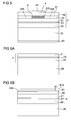
- FIG. 4 A fourth exemplary embodiment of a semiconductor chip according to the invention is shown in FIG FIG. 4 shown in a schematic sectional view.
- This fourth embodiment corresponds essentially to that associated with FIG FIG. 1 described first embodiment.
- the semiconductor body 2 has a tunnel contact layer 34 and a further tunnel contact layer 24.
- the tunnel contact layer 34 and the further tunnel contact layer 24 extend over the entire area over the p-type semiconductor layer 21.
- the injection barrier 5 is formed in the fourth exemplary embodiment by means of a plurality of insulating layers 51, 52 which is arranged on the semiconductor body.
- the injection barrier is thus arranged outside the semiconductor body 2 and is located at least in some areas between the contact 4 and the semiconductor body 2.
- the insulating layers 51 and 52 each form a pair of layers, the layers having different refractive indices from each other.
- a dielectric mirror in the form of a Bragg mirror is formed.
- radiation generated in the direction of the contact 4th is radiated and impinges on the dielectric layers 51, 52, so in the semiconductor body with a relatively high reflectivity, preferably of at least 80%, more preferably at least 90%, are reflected back into the semiconductor body. Subsequently, this radiation can emerge from the semiconductor chip 1.
- the coupling-out efficiency of the semiconductor chip can thus be increased.
- the higher the number of layer pairs the higher the reflectivity of the Bragg mirror can be.
- the injection barrier can simultaneously fulfill the function of a high-efficiency mirror.
- the deposition time also increases. In particular with regard to a short deposition time, therefore, only a single insulation layer may be formed between the semiconductor body 2 and the contact 4 of the exemplary embodiment shown.
- the contact 4 in turn has a contact layer 41 and a mirror layer 42.
- the mirror layer 42 covers the insulation layers 51, 52.
- the radiation generated in the active region 23 of the semiconductor chip 1 and transmitted through the Bragg mirror formed by the insulation layers 51, 52 can thus be reflected back from the mirror layer 42 into the semiconductor body 2.
- a mirror with a particularly high overall reflectivity can be formed.
- radiation components which are transmitted by the Bragg mirror can be reflected back into the semiconductor body by the mirror layer and subsequently emerge from the semiconductor chip 1.
- the contact layer 41 in contrast to in FIG. 1 shown embodiment in the lateral direction to a greater extent than the mirror layer 42.
- the contact layer 41 can thus the mirror layer 42, in particular completely, overmold.
- the contact layer 41 thus extends between the current broadening layer 31 and the injection barrier 5, ie the insulation layers 51, 52.
- the contact layer extends laterally between the mirror layer 42 and the current spreading layer 31.
- charge carriers can be transferred directly from the contact layer into the contact layer Get current spreading layer. Possible rungs are in FIG. 4 again illustrated by arrows.
- the mirror layer 42 can be formed on its side facing away from the semiconductor body independently of the electrical contact properties, in particular with regard to the best possible mirroring of the Bragg mirror formed by means of the insulating layers 51, 52.
- FIG. 5 A fifth exemplary embodiment of a semiconductor chip according to the invention is shown in FIG FIG. 5 shown by a schematic sectional view.
- the current broadening layer 31 is integrated into the semiconductor body 2.
- the current spreading layer 31 is in this case formed by means of a tunnel contact layer 34.
- the contact 4 is arranged on the side facing away from the active region 23 of the tunnel contact layer.
- the injection barrier 5 is as related to FIG. 2 described by means of a portion 240 of the tunnel contact layer 24 formed. In this area the electrical conductivity of the further tunnel contact layer 24 is less than outside this range, ie in a laterally adjacent region 245.
- the tunnel contact layer 34 is sufficiently thick to have a sufficiently high transverse conductivity. Large-area injection of charge carriers outside the injection barrier 5 into the active region 23 is thus simplified. In this case, a current broadening layer arranged outside the semiconductor body can be dispensed with.
- the contact 4 to the semiconductor body 2 preferably has the smallest possible, in particular ohmic, contact resistance.
- the contact layer 41 may also be formed in multiple layers.
- a layer sequence of titanium, platinum and gold is suitable for the contact layer as viewed from the semiconductor body.
- the contact 4 is disposed on the current spreading layer 31.
- the current broadening layer is unstructured in the lateral direction in this embodiment.
- the production of the semiconductor chip is simplified. Deviating from this, however, a recess may be provided in the current broadening layer in which the contact is arranged.
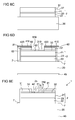
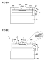
- FIGS. 6A to 6E Shown by means of schematically illustrated intermediate steps in sectional view.
- a semiconductor body 2 is provided with a semiconductor layer sequence.
- the semiconductor layer sequence which forms the semiconductor body 2 is preferably epitaxially deposited, for example by means of MOVPE and MBE, on a carrier 20 which serves as a growth substrate.
- connection layer 32 and a current spreading layer 31 are deposited on the semiconductor body. This is preferably done by means of vapor deposition or sputtering. In this case, first the connection layer and then the current spreading layer 31 are deposited.
- a masking layer 61 is formed, which has a lateral structuring.
- the current spreading layer 31 is exposed.
- the structuring of the masking layer is preferably carried out by means of a lithography process.
- the masking layer is preferably a photosensitive layer, such as a photosensitive resist layer.
- connection layer 32 and the semiconductor body 2 As in FIG. 6C is shown, material of the current spreading layer, the connection layer 32 and the semiconductor body 2, which is located below the recess 610 of the masking layer 61, is removed.
- the current broadening layer and the semiconductor body are thus structured by means of a common masking layer 61 in the lateral direction.
- the connection layer 32 and the semiconductor body 2 After lateral Structuring the current spreading layer 31, the connection layer 32 and the semiconductor body 2, the masking layer can be removed.
- the transfer of the lateral structure of the masking layer 61 to the current spreading layer 31, the connection layer 32 and the semiconductor body 2 preferably takes place in a chemical process, in particular in a wet-chemical etching process or a dry-chemical etching process, such as reactive ion etching or back sputtering.
- a protective layer 7 can now be applied to the semiconductor body, for example by means of sputtering or vapor deposition.
- a further masking layer 62 is applied on the current spreading layer 31, or optionally on the protective layer 7.
- This further masking layer 62 is in turn laterally structured and has a recess 620.
- the lateral structure of the further masking layer 62 is subsequently transferred to the current spreading layer 31 and optionally to the protective layer 7.
- a recess 310 is formed in the current spreading layer. This is preferably again done in a wet-chemical or dry-chemical etching step.
- FIG. 6D shown material for the mirror layer 42 and subsequently deposited material for the contact layer 41 on the semiconductor body 2.
- the deposition of the mirror layer 42 and the contact layer 41 is preferably carried out by means of vapor deposition or sputtering.
- Material 420 for the mirror layer 42 which was applied outside the recess 620 on the further masking layer 62, is lifted off the semiconductor body together with the further masking layer 62. In this case, material 410 for the contact layer 41, which was applied outside the recess 420 on the masking layer 62, is likewise removed.
- the further contact 45 preferably contains a metal, such as gold, silver, nickel, titanium or platinum, or a metallic alloy with at least one of these metals.
- the deposition of the further contact layer is preferably carried out by vapor deposition or sputtering.
- an electrically non-conductive growth substrate it can be removed, for example, in regions, so that a contacting of the semiconductor body by means of the further contact 45 can take place in a region in which the semiconductor body 2 is exposed.
- the growth substrate may also be completely removed or at least thinned.
- the carrier 20 may then be different than the growth substrate.
- a semiconductor chip in which the growth substrate is removed or thinned is also referred to as a thin-film semiconductor chip.
- a basic principle of a thin-film light-emitting diode chip is, for example, in I. Schnitzer et al., Appl. Phys. Lett. 63 (16), 18 October 1993, 2174-2176 described, the disclosure of which is hereby incorporated by reference into the present application.
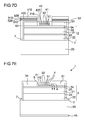
- FIGS. 7A to 7E A second embodiment of a method according to the invention is in the FIGS. 7A to 7E shown schematically.
- a semiconductor body 2 having a semiconductor layer sequence is provided.
- the semiconductor layer sequence of the semiconductor body 2 has as related to FIG. 4 described a tunnel contact layer 34 and a further tunnel contact layer 24.
- a current spreading layer 31 is applied on the semiconductor body 2.
- This Stromverbreiterungs Mrs 31 and the semiconductor body 2 are then as in connection with the Figures 6B and 6C described laterally structured.
- this lateral structuring can in turn be effected by means of a masking layer, which in the FIG. 7B not explicitly shown, done.
- the protective layer 7 can be deposited, for example, by means of vapor deposition or sputtering.
- another masking layer 62 is formed with a recess 620.
- the region of the current widening layer 31 exposed below the recess 620 is removed.
- the current spreading layer 31 may also have only one recess which does not extend completely through the current spreading layer in the vertical direction.
- An alternating sequence of insulating layers 51 and 52 is now deposited on the semiconductor body 2 on the semiconductor body 2.
- the deposition of the insulating layers is preferably carried out by means of sputtering or vapor deposition.
- the insulation layer 51 and the further insulation layer 52 result here as in connection with FIG FIG. 4 indicated a layer pair with layers of different refractive indices.
- a dielectric mirror is formed.
- a mirror layer 42 is deposited on the insulating layers 51, 52.
- the deposition of the insulating layers 51, 52 and the mirror layer 42 is preferably carried out such that these layers in the lateral direction of the Stromverumblerungs Mrs 31 are spaced apart.
- the recess 310 in the Stromverbreiterungs slaughter 31 are formed by wet chemical etching. Due to the resulting undercut, the recess 310 of the Stromverbreiterungs slaughter 31 have a greater lateral extent than the recess 620 of the further masking layer 62nd
- a gap may thus arise between these layers and the current broadening layer.
- a contact layer 41 is deposited, which fills this gap, preferably completely.
- the deposition of the contact layer 41 preferably does not take place from a vertical, but inclined direction to the semiconductor body with simultaneous rotation of the semiconductor body. In this way, the contact layer 41 can completely overmold the mirror layer 42 and the insulation layers 51, 52 in the lateral direction.
- the material for the contact layer 41 may also be deposited in a separate process after the further masking layer 62 has already been removed along with the material thereon.
- the laterally structured forming of the contact layer 41 can take place by means of a third masking layer, which is not explicitly shown in the figures.
- This third masking layer is preferably formed before the deposition of the contact layer on the semiconductor body 2 and laterally structured.
- the third masking layer may have a recess which is larger than the recess 620 of the further masking layer 62.
- FIGS. 8A to 8E Shown by means of schematically illustrated intermediate steps in sectional view.
- the semiconductor body 2 and the current spreading layer 31 formed on the semiconductor body are as described in connection with FIG FIG. 7A described executed.
- FIG. 8B corresponds accordingly to the FIG. 7B ,
- Figure 8A explicitly shows an intermediate step in which one in the FIGS. 7A and 7B Masking layer 61, not shown, is located on the current spreading layer 31.
- a further masking layer 62 having a recess 620 is formed on the current spreading layer 31.
- the lateral structure of the masking layer 62 is transferred into the current spreading layer 31, so that a recess 310 is formed in the current spreading layer 31 below the recess 620 of the further masking layer 62.
- the injection barrier 5 is formed by locally reducing the electrical conductivity of this layer in a region 240 of the further tunnel contact layer 24.
- acceptors in the further tunnel contact layer for example Mg acceptors in an In x Al y Ga 1-xy N semiconductor layer with 0 ⁇ x ⁇ 1 and 0 ⁇ y ⁇ 1, can be electrically deactivated.
- a plasma method is particularly suitable if the region in which the electrical conductivity is to be reduced has a small distance, preferably 100 nm or less, particularly preferably 10 nm or less, to the interface 25 of the semiconductor body 2.
- the conductivity can also be locally reduced by implantation of ions through the recess 620 of the further masking layer 62.
- the crystal structure can be selectively disturbed locally.
- back sputtering such as by an Ar ion beam, suitable.
- backsputtering it is also possible to remove material of the semiconductor body 2.
- FIG. 8E A completed semiconductor chip 1, as related to FIG. 2 is described in is Figure 8E shown.
- This semiconductor chip has a another contact 45 on, as related to FIG. 6E can be described described.
Landscapes
- Led Devices (AREA)
- Semiconductor Lasers (AREA)
- Light Receiving Elements (AREA)
- Electrodes Of Semiconductors (AREA)
Applications Claiming Priority (2)
| Application Number | Priority Date | Filing Date | Title |
|---|---|---|---|
| DE102007032555A DE102007032555A1 (de) | 2007-07-12 | 2007-07-12 | Halbleiterchip und Verfahren zur Herstellung eines Halbleiterchips |
| EP08159845.0A EP2015372B1 (de) | 2007-07-12 | 2008-07-07 | Halbleiterchip und Verfahren zur Herstellung eines Halbleiterchips |
Related Parent Applications (2)
| Application Number | Title | Priority Date | Filing Date |
|---|---|---|---|
| EP08159845.0A Division EP2015372B1 (de) | 2007-07-12 | 2008-07-07 | Halbleiterchip und Verfahren zur Herstellung eines Halbleiterchips |
| EP08159845.0A Division-Into EP2015372B1 (de) | 2007-07-12 | 2008-07-07 | Halbleiterchip und Verfahren zur Herstellung eines Halbleiterchips |
Publications (1)
| Publication Number | Publication Date |
|---|---|
| EP3121858A1 true EP3121858A1 (de) | 2017-01-25 |
Family
ID=39720739
Family Applications (2)
| Application Number | Title | Priority Date | Filing Date |
|---|---|---|---|
| EP16187689.1A Withdrawn EP3121858A1 (de) | 2007-07-12 | 2008-07-07 | Halbleiterchip und verfahren zur herstellung eines halbleiterchips |
| EP08159845.0A Not-in-force EP2015372B1 (de) | 2007-07-12 | 2008-07-07 | Halbleiterchip und Verfahren zur Herstellung eines Halbleiterchips |
Family Applications After (1)
| Application Number | Title | Priority Date | Filing Date |
|---|---|---|---|
| EP08159845.0A Not-in-force EP2015372B1 (de) | 2007-07-12 | 2008-07-07 | Halbleiterchip und Verfahren zur Herstellung eines Halbleiterchips |
Country Status (4)
| Country | Link |
|---|---|
| US (1) | US7994519B2 (enExample) |
| EP (2) | EP3121858A1 (enExample) |
| JP (2) | JP5079611B2 (enExample) |
| DE (1) | DE102007032555A1 (enExample) |
Cited By (1)
| Publication number | Priority date | Publication date | Assignee | Title |
|---|---|---|---|---|
| DE102017104735B4 (de) | 2017-03-07 | 2021-09-02 | OSRAM Opto Semiconductors Gesellschaft mit beschränkter Haftung | Strahlungsemittierender Halbleiterchip |
Families Citing this family (20)
| Publication number | Priority date | Publication date | Assignee | Title |
|---|---|---|---|---|
| DE102007032555A1 (de) | 2007-07-12 | 2009-01-15 | Osram Opto Semiconductors Gmbh | Halbleiterchip und Verfahren zur Herstellung eines Halbleiterchips |
| TWI404189B (zh) * | 2009-02-06 | 2013-08-01 | 億光電子工業股份有限公司 | 複晶式發光二極體元件及其製造方法 |
| JP2010251686A (ja) * | 2009-03-26 | 2010-11-04 | Harison Toshiba Lighting Corp | 発光装置及びその製造方法 |
| US8987772B2 (en) | 2010-11-18 | 2015-03-24 | Seoul Viosys Co., Ltd. | Light emitting diode chip having electrode pad |
| US9520536B2 (en) | 2010-11-18 | 2016-12-13 | Seoul Viosys Co., Ltd. | Light emitting diode chip having electrode pad |
| KR101769075B1 (ko) * | 2010-12-24 | 2017-08-18 | 서울바이오시스 주식회사 | 발광 다이오드 칩 및 그것을 제조하는 방법 |
| JP2014532993A (ja) * | 2011-11-07 | 2014-12-08 | コーニンクレッカ フィリップス エヌ ヴェ | より一様な注入及びより少ない光学的損失を備える改善されたp型接点 |
| DE102012108883A1 (de) * | 2012-09-20 | 2014-03-20 | Osram Opto Semiconductors Gmbh | Optoelektronischer Halbleiterchip und Verfahren zur Herstellung von optoelektronischen Halbleiterchips |
| DE102013007981A1 (de) | 2013-05-10 | 2014-11-13 | Audi Ag | Vorrichtung zum Erzeugen eines Impulses auf ein Fahrzeug in einer Fahrzeugquerrichtung |
| FR3008547B1 (fr) * | 2013-07-15 | 2016-12-09 | Commissariat Energie Atomique | Structure emissive a injection laterale de porteurs |
| CN103594593B (zh) * | 2013-11-08 | 2016-04-06 | 溧阳市江大技术转移中心有限公司 | 具有粗化透明电极的倒装发光二极管的制造方法 |
| KR102131345B1 (ko) * | 2014-02-07 | 2020-07-07 | 엘지이노텍 주식회사 | 발광소자 |
| JP6149878B2 (ja) * | 2015-02-13 | 2017-06-21 | 日亜化学工業株式会社 | 発光素子 |
| DE102015102857A1 (de) * | 2015-02-27 | 2016-09-01 | Osram Opto Semiconductors Gmbh | Optoelektronisches Halbleiterbauelement, Verfahren zur Herstellung eines elektrischen Kontakts und Verfahren zur Herstellung eines Halbleiterbauelements |
| DE102015011635B4 (de) * | 2015-09-11 | 2020-10-08 | Azur Space Solar Power Gmbh | lnfrarot-LED |
| DE102016006295A1 (de) | 2016-05-27 | 2017-11-30 | Azur Space Solar Power Gmbh | Leuchtdiode |
| DE102017002332B4 (de) | 2017-03-13 | 2019-11-07 | Azur Space Solar Power Gmbh | Leuchtdiode |
| DE102017002333A1 (de) * | 2017-03-13 | 2018-09-13 | Azur Space Solar Power Gmbh | Leuchtdiode |
| CN116210093B (zh) * | 2020-11-04 | 2025-09-16 | 苏州晶湛半导体有限公司 | 谐振腔发光二极管及其制备方法 |
| CN115483323A (zh) * | 2021-05-31 | 2022-12-16 | 京东方科技集团股份有限公司 | 发光器件、发光基板和发光器件的制作方法 |
Citations (8)
| Publication number | Priority date | Publication date | Assignee | Title |
|---|---|---|---|---|
| DE19817368A1 (de) * | 1997-04-18 | 1998-12-24 | Epistar Corp | Leuchtdiode |
| US5977566A (en) * | 1996-06-05 | 1999-11-02 | Kabushiki Kaisha Toshiba | Compound semiconductor light emitter |
| DE19937624A1 (de) * | 1999-07-09 | 2001-03-01 | Epistar Corp | Leuchtdiode mit einer großen Helligkeit |
| US6420732B1 (en) * | 2000-06-26 | 2002-07-16 | Luxnet Corporation | Light emitting diode of improved current blocking and light extraction structure |
| US6693352B1 (en) * | 2000-06-05 | 2004-02-17 | Emitronix Inc. | Contact structure for group III-V semiconductor devices and method of producing the same |
| DE102005008056A1 (de) * | 2004-12-30 | 2006-07-13 | Osram Opto Semiconductors Gmbh | Strahlungsemittierender Halbleiterchip und Verfahren zur Herstellung eines solchen Halbleiterchips |
| DE102005061797A1 (de) * | 2005-12-23 | 2007-07-05 | Osram Opto Semiconductors Gmbh | Lumineszenzdiodenchip mit Stromaufweitungsschicht und Verfahren zu dessen Herstellung |
| DE102007032555A1 (de) | 2007-07-12 | 2009-01-15 | Osram Opto Semiconductors Gmbh | Halbleiterchip und Verfahren zur Herstellung eines Halbleiterchips |
Family Cites Families (17)
| Publication number | Priority date | Publication date | Assignee | Title |
|---|---|---|---|---|
| JP2856374B2 (ja) * | 1992-02-24 | 1999-02-10 | シャープ株式会社 | 半導体発光素子及びその製造方法 |
| JPH08148716A (ja) * | 1994-11-15 | 1996-06-07 | Rohm Co Ltd | 半導体発光素子とその製造方法 |
| US6078064A (en) | 1998-05-04 | 2000-06-20 | Epistar Co. | Indium gallium nitride light emitting diode |
| JP3638515B2 (ja) * | 2000-09-29 | 2005-04-13 | 株式会社東芝 | 垂直共振器型半導体発光素子 |
| JP2003017806A (ja) * | 2001-06-29 | 2003-01-17 | Toshiba Corp | 化合物半導体発光素子とその製造方法および化合物半導体発光装置 |
| US6515308B1 (en) * | 2001-12-21 | 2003-02-04 | Xerox Corporation | Nitride-based VCSEL or light emitting diode with p-n tunnel junction current injection |
| JP2004111648A (ja) * | 2002-09-18 | 2004-04-08 | Hamamatsu Photonics Kk | 半導体発光素子 |
| JP2003282946A (ja) * | 2003-02-06 | 2003-10-03 | Matsushita Electric Ind Co Ltd | 発光ダイオード装置及びその製造方法 |
| JP4135550B2 (ja) * | 2003-04-18 | 2008-08-20 | 日立電線株式会社 | 半導体発光デバイス |
| DE10346605B4 (de) * | 2003-08-29 | 2022-02-24 | OSRAM Opto Semiconductors Gesellschaft mit beschränkter Haftung | Strahlungemittierendes Halbleiterbauelement |
| KR100853882B1 (ko) | 2003-08-29 | 2008-08-22 | 오스람 옵토 세미컨덕터스 게엠베하 | 방사선 방출 반도체 소자 |
| US7009215B2 (en) * | 2003-10-24 | 2006-03-07 | General Electric Company | Group III-nitride based resonant cavity light emitting devices fabricated on single crystal gallium nitride substrates |
| US7808011B2 (en) * | 2004-03-19 | 2010-10-05 | Koninklijke Philips Electronics N.V. | Semiconductor light emitting devices including in-plane light emitting layers |
| JP2005268601A (ja) * | 2004-03-19 | 2005-09-29 | Sumitomo Chemical Co Ltd | 化合物半導体発光素子 |
| JP4833537B2 (ja) * | 2004-10-07 | 2011-12-07 | フィリップス ルミレッズ ライティング カンパニー リミテッド ライアビリティ カンパニー | 半導体発光素子 |
| KR100738554B1 (ko) * | 2006-01-26 | 2007-07-11 | 삼성전자주식회사 | 듀얼모드 단말에서의 호 처리 장치 및 방법 |
| US7573074B2 (en) * | 2006-05-19 | 2009-08-11 | Bridgelux, Inc. | LED electrode |
-
2007
- 2007-07-12 DE DE102007032555A patent/DE102007032555A1/de not_active Withdrawn
-
2008
- 2008-07-07 EP EP16187689.1A patent/EP3121858A1/de not_active Withdrawn
- 2008-07-07 EP EP08159845.0A patent/EP2015372B1/de not_active Not-in-force
- 2008-07-10 JP JP2008180584A patent/JP5079611B2/ja active Active
- 2008-07-14 US US12/218,492 patent/US7994519B2/en active Active
-
2012
- 2012-08-29 JP JP2012188817A patent/JP5876792B2/ja not_active Expired - Fee Related
Patent Citations (8)
| Publication number | Priority date | Publication date | Assignee | Title |
|---|---|---|---|---|
| US5977566A (en) * | 1996-06-05 | 1999-11-02 | Kabushiki Kaisha Toshiba | Compound semiconductor light emitter |
| DE19817368A1 (de) * | 1997-04-18 | 1998-12-24 | Epistar Corp | Leuchtdiode |
| DE19937624A1 (de) * | 1999-07-09 | 2001-03-01 | Epistar Corp | Leuchtdiode mit einer großen Helligkeit |
| US6693352B1 (en) * | 2000-06-05 | 2004-02-17 | Emitronix Inc. | Contact structure for group III-V semiconductor devices and method of producing the same |
| US6420732B1 (en) * | 2000-06-26 | 2002-07-16 | Luxnet Corporation | Light emitting diode of improved current blocking and light extraction structure |
| DE102005008056A1 (de) * | 2004-12-30 | 2006-07-13 | Osram Opto Semiconductors Gmbh | Strahlungsemittierender Halbleiterchip und Verfahren zur Herstellung eines solchen Halbleiterchips |
| DE102005061797A1 (de) * | 2005-12-23 | 2007-07-05 | Osram Opto Semiconductors Gmbh | Lumineszenzdiodenchip mit Stromaufweitungsschicht und Verfahren zu dessen Herstellung |
| DE102007032555A1 (de) | 2007-07-12 | 2009-01-15 | Osram Opto Semiconductors Gmbh | Halbleiterchip und Verfahren zur Herstellung eines Halbleiterchips |
Non-Patent Citations (2)
| Title |
|---|
| I. SCHNITZER ET AL., APPL. PHYS. LETT., vol. 63, no. 16, 18 October 1993 (1993-10-18), pages 2174 - 2176 |
| JEON SEONG-RAN ET AL: "Lateral current spreading in GaN-based light-emitting diodes utilizing tunnel contact junctions", APPLIED PHYSICS LETTERS, AIP, AMERICAN INSTITUTE OF PHYSICS, MELVILLE, NY, US, vol. 78, no. 21, 21 May 2001 (2001-05-21), pages 3265 - 3267, XP012028099, ISSN: 0003-6951, DOI: 10.1063/1.1374483 * |
Cited By (1)
| Publication number | Priority date | Publication date | Assignee | Title |
|---|---|---|---|---|
| DE102017104735B4 (de) | 2017-03-07 | 2021-09-02 | OSRAM Opto Semiconductors Gesellschaft mit beschränkter Haftung | Strahlungsemittierender Halbleiterchip |
Also Published As
| Publication number | Publication date |
|---|---|
| JP5876792B2 (ja) | 2016-03-02 |
| JP2012256933A (ja) | 2012-12-27 |
| EP2015372A2 (de) | 2009-01-14 |
| US7994519B2 (en) | 2011-08-09 |
| EP2015372B1 (de) | 2016-10-19 |
| EP2015372A3 (de) | 2013-02-06 |
| DE102007032555A1 (de) | 2009-01-15 |
| JP2009033157A (ja) | 2009-02-12 |
| US20090045426A1 (en) | 2009-02-19 |
| JP5079611B2 (ja) | 2012-11-21 |
Similar Documents
| Publication | Publication Date | Title |
|---|---|---|
| EP2015372B1 (de) | Halbleiterchip und Verfahren zur Herstellung eines Halbleiterchips | |
| EP3200247B1 (de) | Halbleiterchip und verfahren zur herstellung eines halbleiterchips | |
| EP3128555B1 (de) | Leuchtdiodenchip mit integriertem schutz gegen elektrostatische entladungen und entsprechendes herstellungsverfahren | |
| EP2011160B1 (de) | Optoelektronischer halbleiterchip | |
| DE102010024079B4 (de) | Verfahren zur Herstellung eines optoelektronischen Halbleiterchips und optoelektronischer Halbleiterchip | |
| EP2193555B1 (de) | Optoelektronischer halbleiterkörper | |
| EP2149159A1 (de) | Optoelektronischer halbleiterkörper und verfahren zur herstellung eines solchen | |
| EP1906460A2 (de) | Halbleiterkörper und Halbleiterchip mit einem Halbleiterkörper | |
| EP2980864B1 (de) | Optoelektronischer halbleiterchip und verfahren zur herstellung eines optoelektronischen halbleiterchips | |
| EP1658643B1 (de) | Strahlungemittierendes halbleiterbauelement | |
| DE102016124847B4 (de) | Optoelektronischer Halbleiterchip und Verfahren zur Herstellung eines optoelektronischen Halbleiterchips | |
| DE10346605B4 (de) | Strahlungemittierendes Halbleiterbauelement | |
| WO2008089739A1 (de) | Halbleiterchip und verfahren zur herstellung eines halbleiterchips | |
| DE10203809A1 (de) | Strahlungsemittierendes Halbleiterbauelement | |
| DE102015116865B4 (de) | Verfahren zur Herstellung eines Halbleiterchips und Halbleiterchip | |
| WO2018114483A1 (de) | Optoelektronischer halbleiterchip und verfahren zur herstellung eines optoelektronischen halbleiterchips | |
| EP1430519A2 (de) | Verfahren zur herstellung eines halbleiterbauelements auf der basis eines nitrid-verbindungshalbleiters | |
| DE102014107306A1 (de) | Verfahren zur Herstellung eines optoelektronischen Halbleiterchips und optoelektronischer Halbleiterchip | |
| DE102018122492A1 (de) | Optoelektronisches halbleiterbauelement mit einer ersten und zweiten metallschicht sowie verfahren zur herstellung des optoelektronischen halbleiterbauelements |
Legal Events
| Date | Code | Title | Description |
|---|---|---|---|
| PUAI | Public reference made under article 153(3) epc to a published international application that has entered the european phase |
Free format text: ORIGINAL CODE: 0009012 |
|
| AC | Divisional application: reference to earlier application |
Ref document number: 2015372 Country of ref document: EP Kind code of ref document: P |
|
| AK | Designated contracting states |
Kind code of ref document: A1 Designated state(s): AT BE BG CH CY CZ DE DK EE ES FI FR GB GR HR HU IE IS IT LI LT LU LV MC MT NL NO PL PT RO SE SI SK TR |
|
| 17P | Request for examination filed |
Effective date: 20170712 |
|
| RBV | Designated contracting states (corrected) |
Designated state(s): AT BE BG CH CY CZ DE DK EE ES FI FR GB GR HR HU IE IS IT LI LT LU LV MC MT NL NO PL PT RO SE SI SK TR |
|
| GRAP | Despatch of communication of intention to grant a patent |
Free format text: ORIGINAL CODE: EPIDOSNIGR1 |
|
| RIC1 | Information provided on ipc code assigned before grant |
Ipc: H01L 33/14 20100101ALI20180723BHEP Ipc: H01L 33/38 20100101ALN20180723BHEP Ipc: H01L 33/40 20100101ALN20180723BHEP Ipc: H01L 33/04 20100101ALI20180723BHEP Ipc: H01L 33/42 20100101ALN20180723BHEP Ipc: H01L 33/00 20100101AFI20180723BHEP |
|
| INTG | Intention to grant announced |
Effective date: 20180820 |
|
| STAA | Information on the status of an ep patent application or granted ep patent |
Free format text: STATUS: THE APPLICATION IS DEEMED TO BE WITHDRAWN |
|
| 18D | Application deemed to be withdrawn |
Effective date: 20190103 |