EP3121834A1 - Bezugsmarke für tem/stem-tomografie-neigeserie-erfassung und ausrichtung - Google Patents
Bezugsmarke für tem/stem-tomografie-neigeserie-erfassung und ausrichtung Download PDFInfo
- Publication number
- EP3121834A1 EP3121834A1 EP16158607.8A EP16158607A EP3121834A1 EP 3121834 A1 EP3121834 A1 EP 3121834A1 EP 16158607 A EP16158607 A EP 16158607A EP 3121834 A1 EP3121834 A1 EP 3121834A1
- Authority
- EP
- European Patent Office
- Prior art keywords
- sample
- fiducial
- holes
- pillar
- hole
- Prior art date
- Legal status (The legal status is an assumption and is not a legal conclusion. Google has not performed a legal analysis and makes no representation as to the accuracy of the status listed.)
- Withdrawn
Links
Images


Classifications
-
- H—ELECTRICITY
- H01—ELECTRIC ELEMENTS
- H01J—ELECTRIC DISCHARGE TUBES OR DISCHARGE LAMPS
- H01J37/00—Discharge tubes with provision for introducing objects or material to be exposed to the discharge, e.g. for the purpose of examination or processing thereof
- H01J37/02—Details
- H01J37/22—Optical or photographic arrangements associated with the tube
- H01J37/222—Image processing arrangements associated with the tube
-
- G—PHYSICS
- G01—MEASURING; TESTING
- G01N—INVESTIGATING OR ANALYSING MATERIALS BY DETERMINING THEIR CHEMICAL OR PHYSICAL PROPERTIES
- G01N23/00—Investigating or analysing materials by the use of wave or particle radiation, e.g. X-rays or neutrons, not covered by groups G01N3/00 – G01N17/00, G01N21/00 or G01N22/00
- G01N23/22—Investigating or analysing materials by the use of wave or particle radiation, e.g. X-rays or neutrons, not covered by groups G01N3/00 – G01N17/00, G01N21/00 or G01N22/00 by measuring secondary emission from the material
-
- H—ELECTRICITY
- H01—ELECTRIC ELEMENTS
- H01J—ELECTRIC DISCHARGE TUBES OR DISCHARGE LAMPS
- H01J37/00—Discharge tubes with provision for introducing objects or material to be exposed to the discharge, e.g. for the purpose of examination or processing thereof
- H01J37/26—Electron or ion microscopes; Electron or ion diffraction tubes
- H01J37/28—Electron or ion microscopes; Electron or ion diffraction tubes with scanning beams
-
- G—PHYSICS
- G01—MEASURING; TESTING
- G01N—INVESTIGATING OR ANALYSING MATERIALS BY DETERMINING THEIR CHEMICAL OR PHYSICAL PROPERTIES
- G01N23/00—Investigating or analysing materials by the use of wave or particle radiation, e.g. X-rays or neutrons, not covered by groups G01N3/00 – G01N17/00, G01N21/00 or G01N22/00
- G01N23/02—Investigating or analysing materials by the use of wave or particle radiation, e.g. X-rays or neutrons, not covered by groups G01N3/00 – G01N17/00, G01N21/00 or G01N22/00 by transmitting the radiation through the material
- G01N23/04—Investigating or analysing materials by the use of wave or particle radiation, e.g. X-rays or neutrons, not covered by groups G01N3/00 – G01N17/00, G01N21/00 or G01N22/00 by transmitting the radiation through the material and forming images of the material
- G01N23/046—Investigating or analysing materials by the use of wave or particle radiation, e.g. X-rays or neutrons, not covered by groups G01N3/00 – G01N17/00, G01N21/00 or G01N22/00 by transmitting the radiation through the material and forming images of the material using tomography, e.g. computed tomography [CT]
-
- G—PHYSICS
- G01—MEASURING; TESTING
- G01N—INVESTIGATING OR ANALYSING MATERIALS BY DETERMINING THEIR CHEMICAL OR PHYSICAL PROPERTIES
- G01N1/00—Sampling; Preparing specimens for investigation
- G01N1/28—Preparing specimens for investigation including physical details of (bio-)chemical methods covered elsewhere, e.g. G01N33/50, C12Q
- G01N1/32—Polishing; Etching
-
- H—ELECTRICITY
- H01—ELECTRIC ELEMENTS
- H01J—ELECTRIC DISCHARGE TUBES OR DISCHARGE LAMPS
- H01J2237/00—Discharge tubes exposing object to beam, e.g. for analysis treatment, etching, imaging
- H01J2237/22—Treatment of data
- H01J2237/226—Image reconstruction
-
- H—ELECTRICITY
- H01—ELECTRIC ELEMENTS
- H01J—ELECTRIC DISCHARGE TUBES OR DISCHARGE LAMPS
- H01J2237/00—Discharge tubes exposing object to beam, e.g. for analysis treatment, etching, imaging
- H01J2237/26—Electron or ion microscopes
- H01J2237/2611—Stereoscopic measurements and/or imaging
-
- H—ELECTRICITY
- H01—ELECTRIC ELEMENTS
- H01J—ELECTRIC DISCHARGE TUBES OR DISCHARGE LAMPS
- H01J2237/00—Discharge tubes exposing object to beam, e.g. for analysis treatment, etching, imaging
- H01J2237/26—Electron or ion microscopes
- H01J2237/28—Scanning microscopes
- H01J2237/2802—Transmission microscopes
-
- H—ELECTRICITY
- H01—ELECTRIC ELEMENTS
- H01J—ELECTRIC DISCHARGE TUBES OR DISCHARGE LAMPS
- H01J2237/00—Discharge tubes exposing object to beam, e.g. for analysis treatment, etching, imaging
- H01J2237/26—Electron or ion microscopes
- H01J2237/282—Determination of microscope properties
- H01J2237/2826—Calibration
-
- H—ELECTRICITY
- H01—ELECTRIC ELEMENTS
- H01J—ELECTRIC DISCHARGE TUBES OR DISCHARGE LAMPS
- H01J2237/00—Discharge tubes exposing object to beam, e.g. for analysis treatment, etching, imaging
- H01J2237/30—Electron or ion beam tubes for processing objects
- H01J2237/304—Controlling tubes
- H01J2237/30433—System calibration
- H01J2237/30438—Registration
-
- H—ELECTRICITY
- H01—ELECTRIC ELEMENTS
- H01J—ELECTRIC DISCHARGE TUBES OR DISCHARGE LAMPS
- H01J37/00—Discharge tubes with provision for introducing objects or material to be exposed to the discharge, e.g. for the purpose of examination or processing thereof
- H01J37/30—Electron-beam or ion-beam tubes for localised treatment of objects
- H01J37/304—Controlling tubes by information coming from the objects or from the beam, e.g. correction signals
- H01J37/3045—Object or beam position registration
Landscapes
- Analytical Chemistry (AREA)
- Chemical & Material Sciences (AREA)
- Health & Medical Sciences (AREA)
- Engineering & Computer Science (AREA)
- General Health & Medical Sciences (AREA)
- Pathology (AREA)
- Life Sciences & Earth Sciences (AREA)
- Biochemistry (AREA)
- Physics & Mathematics (AREA)
- General Physics & Mathematics (AREA)
- Immunology (AREA)
- Radiology & Medical Imaging (AREA)
- Nuclear Medicine, Radiotherapy & Molecular Imaging (AREA)
- Pulmonology (AREA)
- Theoretical Computer Science (AREA)
- Computer Vision & Pattern Recognition (AREA)
- Analysing Materials By The Use Of Radiation (AREA)
- Sampling And Sample Adjustment (AREA)
Applications Claiming Priority (1)
| Application Number | Priority Date | Filing Date | Title |
|---|---|---|---|
| US201562196246P | 2015-07-23 | 2015-07-23 |
Publications (1)
| Publication Number | Publication Date |
|---|---|
| EP3121834A1 true EP3121834A1 (de) | 2017-01-25 |
Family
ID=57836148
Family Applications (1)
| Application Number | Title | Priority Date | Filing Date |
|---|---|---|---|
| EP16158607.8A Withdrawn EP3121834A1 (de) | 2015-07-23 | 2016-03-04 | Bezugsmarke für tem/stem-tomografie-neigeserie-erfassung und ausrichtung |
Country Status (4)
| Country | Link |
|---|---|
| US (1) | US9627176B2 (de) |
| EP (1) | EP3121834A1 (de) |
| JP (1) | JP6393448B2 (de) |
| CN (1) | CN106370680B (de) |
Cited By (1)
| Publication number | Priority date | Publication date | Assignee | Title |
|---|---|---|---|---|
| CN112903733A (zh) * | 2021-01-25 | 2021-06-04 | 中国科学院广州地球化学研究所 | 一种透射电镜能谱超分辨分析方法 |
Families Citing this family (6)
| Publication number | Priority date | Publication date | Assignee | Title |
|---|---|---|---|---|
| DE102017212020B3 (de) * | 2017-07-13 | 2018-05-30 | Carl Zeiss Microscopy Gmbh | Verfahren zur In-situ-Präparation und zum Transfer mikroskopischer Proben, Computerprogrammprodukt sowie mikroskopische Probe |
| JP7154531B2 (ja) * | 2018-03-22 | 2022-10-18 | 国立大学法人東北大学 | 電子デバイスの評価方法および評価装置 |
| US10695844B2 (en) | 2018-06-17 | 2020-06-30 | Arevo, Inc. | Registration of articles of manufacture with dimensional variations |
| US20220254060A1 (en) * | 2021-02-09 | 2022-08-11 | Fei Company | 3d fiducial for precision 3d nand channel tilt/shift analysis |
| US11476079B1 (en) * | 2021-03-31 | 2022-10-18 | Fei Company | Method and system for imaging a multi-pillar sample |
| CN117553723B (zh) * | 2024-01-12 | 2024-04-23 | 中铁大桥局集团有限公司 | 一种基于三维扫描技术的预埋件装配板孔群的定位方法 |
Citations (3)
| Publication number | Priority date | Publication date | Assignee | Title |
|---|---|---|---|---|
| EP2056332A1 (de) * | 2007-10-29 | 2009-05-06 | Hitachi High-Technologies Corporation | Versatzkorrektur eines Probenhalters für eine euzentrische Drehungen in einem Teilchenstrahlmikroskop |
| US20100288925A1 (en) * | 2005-04-06 | 2010-11-18 | Edward Principe | High-density FIB-SEM tomography via real-time imaging |
| US7884326B2 (en) | 2007-01-22 | 2011-02-08 | Fei Company | Manipulator for rotating and translating a sample holder |
Family Cites Families (9)
| Publication number | Priority date | Publication date | Assignee | Title |
|---|---|---|---|---|
| US7442924B2 (en) | 2005-02-23 | 2008-10-28 | Fei, Company | Repetitive circumferential milling for sample preparation |
| TWI372859B (en) * | 2008-10-03 | 2012-09-21 | Inotera Memories Inc | Method for manufacturing an electron tomography specimen with fiducial markers and method for constructing 3d image |
| JP5321918B2 (ja) * | 2010-06-15 | 2013-10-23 | 独立行政法人産業技術総合研究所 | 電子顕微鏡用試料作製方法 |
| EP2402976A1 (de) | 2010-06-30 | 2012-01-04 | Fei Company | Verfahren zur Elektrondiffraktionstomografie |
| EP2708874A1 (de) | 2012-09-12 | 2014-03-19 | Fei Company | Verfahren zur Durchführung von Tomographiebildgebung einer Probe in einem Mikroskop mit geladenen Teilchen |
| EP2738786A1 (de) | 2012-11-29 | 2014-06-04 | Fei Company | Verfahren zur Durchführung von Tomographiebildgebung einer Probe in einem Ladungsträger-Mikroskop |
| US10026590B2 (en) * | 2012-12-31 | 2018-07-17 | Fei Company | Fiducial design for tilted or glancing mill operations with a charged particle beam |
| EP2811288B1 (de) | 2013-06-06 | 2016-08-10 | Fei Company | Verfahren zur Elektronentomographie |
| EP2916342A1 (de) | 2014-03-05 | 2015-09-09 | Fei Company | Herstellung einer Lamelle zur korrelativen tomografischen Analyse mit atomarer Auflösung |
-
2016
- 2016-01-06 US US14/989,419 patent/US9627176B2/en active Active
- 2016-03-04 EP EP16158607.8A patent/EP3121834A1/de not_active Withdrawn
- 2016-07-18 JP JP2016140965A patent/JP6393448B2/ja active Active
- 2016-07-22 CN CN201610806416.1A patent/CN106370680B/zh active Active
Patent Citations (3)
| Publication number | Priority date | Publication date | Assignee | Title |
|---|---|---|---|---|
| US20100288925A1 (en) * | 2005-04-06 | 2010-11-18 | Edward Principe | High-density FIB-SEM tomography via real-time imaging |
| US7884326B2 (en) | 2007-01-22 | 2011-02-08 | Fei Company | Manipulator for rotating and translating a sample holder |
| EP2056332A1 (de) * | 2007-10-29 | 2009-05-06 | Hitachi High-Technologies Corporation | Versatzkorrektur eines Probenhalters für eine euzentrische Drehungen in einem Teilchenstrahlmikroskop |
Non-Patent Citations (2)
| Title |
|---|
| HAYASHIDA M ET AL: "High-precision alignment of electron tomography tilt series using markers formed in helium-ion microscope", MICRON, vol. 50, 11 April 2013 (2013-04-11), pages 29 - 34, XP028674028, ISSN: 0968-4328, DOI: 10.1016/J.MICRON.2013.04.002 * |
| MILLER M K ET AL: "Strategies for fabricating atom probe specimens with a dual beam FIB", ULTRAMICROSCOPY, ELSEVIER, AMSTERDAM, NL, vol. 102, no. 4, 20 November 2004 (2004-11-20), pages 287 - 298, XP027655371, ISSN: 0304-3991, [retrieved on 20050301] * |
Cited By (2)
| Publication number | Priority date | Publication date | Assignee | Title |
|---|---|---|---|---|
| CN112903733A (zh) * | 2021-01-25 | 2021-06-04 | 中国科学院广州地球化学研究所 | 一种透射电镜能谱超分辨分析方法 |
| CN112903733B (zh) * | 2021-01-25 | 2022-07-29 | 中国科学院广州地球化学研究所 | 一种透射电镜能谱超分辨分析方法 |
Also Published As
| Publication number | Publication date |
|---|---|
| JP2017026612A (ja) | 2017-02-02 |
| CN106370680A (zh) | 2017-02-01 |
| US20170025246A1 (en) | 2017-01-26 |
| CN106370680B (zh) | 2019-04-23 |
| JP6393448B2 (ja) | 2018-09-19 |
| US9627176B2 (en) | 2017-04-18 |
Similar Documents
| Publication | Publication Date | Title |
|---|---|---|
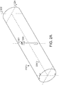
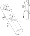
| US9627176B2 (en) | Fiducial formation for TEM/STEM tomography tilt-series acquisition and alignment | |
| CN106165055B (zh) | 对样品进行电子衍射图案分析的方法 | |
| US8476588B2 (en) | Method of electron diffraction tomography | |
| KR102056507B1 (ko) | 하전 입자 빔 장치 및 시료 관찰 방법 | |
| WO2010125754A1 (ja) | 複合荷電粒子線装置 | |
| US9797923B2 (en) | Fabrication of a malleable lamella for correlative atomic-resolution tomographic analyses | |
| EP2811288B1 (de) | Verfahren zur Elektronentomographie | |
| KR102590634B1 (ko) | 하전 입자 빔 장치, 시료 가공 방법 | |
| JP5309552B2 (ja) | 電子線トモグラフィ法及び電子線トモグラフィ装置 | |
| JP2017174503A (ja) | 集束イオンビーム装置 | |
| US9514913B2 (en) | TEM sample mounting geometry | |
| US10937625B2 (en) | Method of imaging a sample using an electron microscope | |
| KR20150092087A (ko) | 하전 입자 빔 샘플 준비과정에서 커트닝을 감소하기 위한 방법 및 시스템 | |
| JP4433092B2 (ja) | 三次元構造観察方法 | |
| JP7138066B2 (ja) | 歳差電子回折データマッピングのために走査型透過電子顕微鏡を自動的にアライメントする方法 | |
| JP4988175B2 (ja) | 荷電粒子装置用試料台 | |
| TWI813760B (zh) | 試料加工觀察方法 | |
| JP4393352B2 (ja) | 電子顕微鏡 | |
| CN114689630A (zh) | 用于对三维特征进行成像的方法和系统 | |
| KR20210056407A (ko) | 화상 형성 방법 및 화상 형성 시스템 | |
| JP4232848B2 (ja) | 3次元構造観察用試料作製装置、電子顕微鏡及びその方法 | |
| EP3392900B1 (de) | Verfahren zur automatischen ausrichtung eines rastertransmission-elektronenmikroskops für präzessionselektronenbeugungsdatenmapping | |
| JP2008262921A (ja) | 3次元構造観察用試料作製装置、電子顕微鏡及びその方法 | |
| CN117849084A (zh) | 从大块样品中制备感兴趣体积的方法及计算机程序产品 | |
| EP3125270A1 (de) | Tem-probenbefestigungsgeometrie |
Legal Events
| Date | Code | Title | Description |
|---|---|---|---|
| PUAI | Public reference made under article 153(3) epc to a published international application that has entered the european phase |
Free format text: ORIGINAL CODE: 0009012 |
|
| AK | Designated contracting states |
Kind code of ref document: A1 Designated state(s): AL AT BE BG CH CY CZ DE DK EE ES FI FR GB GR HR HU IE IS IT LI LT LU LV MC MK MT NL NO PL PT RO RS SE SI SK SM TR |
|
| AX | Request for extension of the european patent |
Extension state: BA ME |
|
| 17P | Request for examination filed |
Effective date: 20170725 |
|
| RBV | Designated contracting states (corrected) |
Designated state(s): AL AT BE BG CH CY CZ DE DK EE ES FI FR GB GR HR HU IE IS IT LI LT LU LV MC MK MT NL NO PL PT RO RS SE SI SK SM TR |
|
| STAA | Information on the status of an ep patent application or granted ep patent |
Free format text: STATUS: THE APPLICATION IS DEEMED TO BE WITHDRAWN |
|
| 18D | Application deemed to be withdrawn |
Effective date: 20170726 |