EP2916342A1 - Herstellung einer Lamelle zur korrelativen tomografischen Analyse mit atomarer Auflösung - Google Patents
Herstellung einer Lamelle zur korrelativen tomografischen Analyse mit atomarer Auflösung Download PDFInfo
- Publication number
- EP2916342A1 EP2916342A1 EP14169243.4A EP14169243A EP2916342A1 EP 2916342 A1 EP2916342 A1 EP 2916342A1 EP 14169243 A EP14169243 A EP 14169243A EP 2916342 A1 EP2916342 A1 EP 2916342A1
- Authority
- EP
- European Patent Office
- Prior art keywords
- lamella
- interest
- region
- sample
- forming
- Prior art date
- Legal status (The legal status is an assumption and is not a legal conclusion. Google has not performed a legal analysis and makes no representation as to the accuracy of the status listed.)
- Withdrawn
Links
Images


Classifications
-
- G—PHYSICS
- G01—MEASURING; TESTING
- G01Q—SCANNING-PROBE TECHNIQUES OR APPARATUS; APPLICATIONS OF SCANNING-PROBE TECHNIQUES, e.g. SCANNING PROBE MICROSCOPY [SPM]
- G01Q30/00—Auxiliary means serving to assist or improve the scanning probe techniques or apparatus, e.g. display or data processing devices
- G01Q30/02—Non-SPM analysing devices, e.g. SEM [Scanning Electron Microscope], spectrometer or optical microscope
-
- G—PHYSICS
- G01—MEASURING; TESTING
- G01N—INVESTIGATING OR ANALYSING MATERIALS BY DETERMINING THEIR CHEMICAL OR PHYSICAL PROPERTIES
- G01N1/00—Sampling; Preparing specimens for investigation
-
- G—PHYSICS
- G01—MEASURING; TESTING
- G01N—INVESTIGATING OR ANALYSING MATERIALS BY DETERMINING THEIR CHEMICAL OR PHYSICAL PROPERTIES
- G01N1/00—Sampling; Preparing specimens for investigation
- G01N1/28—Preparing specimens for investigation including physical details of (bio-)chemical methods covered elsewhere, e.g. G01N33/50, C12Q
- G01N1/32—Polishing; Etching
-
- G—PHYSICS
- G01—MEASURING; TESTING
- G01Q—SCANNING-PROBE TECHNIQUES OR APPARATUS; APPLICATIONS OF SCANNING-PROBE TECHNIQUES, e.g. SCANNING PROBE MICROSCOPY [SPM]
- G01Q30/00—Auxiliary means serving to assist or improve the scanning probe techniques or apparatus, e.g. display or data processing devices
- G01Q30/20—Sample handling devices or methods
-
- H—ELECTRICITY
- H01—ELECTRIC ELEMENTS
- H01J—ELECTRIC DISCHARGE TUBES OR DISCHARGE LAMPS
- H01J37/00—Discharge tubes with provision for introducing objects or material to be exposed to the discharge, e.g. for the purpose of examination or processing thereof
- H01J37/26—Electron or ion microscopes; Electron or ion diffraction tubes
- H01J37/285—Emission microscopes, e.g. field-emission microscopes
-
- G—PHYSICS
- G01—MEASURING; TESTING
- G01N—INVESTIGATING OR ANALYSING MATERIALS BY DETERMINING THEIR CHEMICAL OR PHYSICAL PROPERTIES
- G01N1/00—Sampling; Preparing specimens for investigation
- G01N1/28—Preparing specimens for investigation including physical details of (bio-)chemical methods covered elsewhere, e.g. G01N33/50, C12Q
- G01N1/2813—Producing thin layers of samples on a substrate, e.g. smearing, spinning-on
- G01N2001/282—Producing thin layers of samples on a substrate, e.g. smearing, spinning-on with mapping; Identification of areas; Spatial correlated pattern
-
- H—ELECTRICITY
- H01—ELECTRIC ELEMENTS
- H01J—ELECTRIC DISCHARGE TUBES OR DISCHARGE LAMPS
- H01J2237/00—Discharge tubes exposing object to beam, e.g. for analysis treatment, etching, imaging
- H01J2237/26—Electron or ion microscopes
- H01J2237/28—Scanning microscopes
- H01J2237/2802—Transmission microscopes
-
- H—ELECTRICITY
- H01—ELECTRIC ELEMENTS
- H01J—ELECTRIC DISCHARGE TUBES OR DISCHARGE LAMPS
- H01J2237/00—Discharge tubes exposing object to beam, e.g. for analysis treatment, etching, imaging
- H01J2237/26—Electron or ion microscopes
- H01J2237/285—Emission microscopes
- H01J2237/2852—Auto-emission (i.e. field-emission)
-
- H—ELECTRICITY
- H01—ELECTRIC ELEMENTS
- H01J—ELECTRIC DISCHARGE TUBES OR DISCHARGE LAMPS
- H01J2237/00—Discharge tubes exposing object to beam, e.g. for analysis treatment, etching, imaging
- H01J2237/30—Electron or ion beam tubes for processing objects
- H01J2237/317—Processing objects on a microscale
- H01J2237/3174—Etching microareas
- H01J2237/31745—Etching microareas for preparing specimen to be viewed in microscopes or analyzed in microanalysers
-
- H—ELECTRICITY
- H01—ELECTRIC ELEMENTS
- H01J—ELECTRIC DISCHARGE TUBES OR DISCHARGE LAMPS
- H01J2237/00—Discharge tubes exposing object to beam, e.g. for analysis treatment, etching, imaging
- H01J2237/30—Electron or ion beam tubes for processing objects
- H01J2237/317—Processing objects on a microscale
- H01J2237/31749—Focused ion beam
-
- Y—GENERAL TAGGING OF NEW TECHNOLOGICAL DEVELOPMENTS; GENERAL TAGGING OF CROSS-SECTIONAL TECHNOLOGIES SPANNING OVER SEVERAL SECTIONS OF THE IPC; TECHNICAL SUBJECTS COVERED BY FORMER USPC CROSS-REFERENCE ART COLLECTIONS [XRACs] AND DIGESTS
- Y10—TECHNICAL SUBJECTS COVERED BY FORMER USPC
- Y10T—TECHNICAL SUBJECTS COVERED BY FORMER US CLASSIFICATION
- Y10T428/00—Stock material or miscellaneous articles
- Y10T428/29—Coated or structually defined flake, particle, cell, strand, strand portion, rod, filament, macroscopic fiber or mass thereof
- Y10T428/2913—Rod, strand, filament or fiber
- Y10T428/2933—Coated or with bond, impregnation or core
- Y10T428/294—Coated or with bond, impregnation or core including metal or compound thereof [excluding glass, ceramic and asbestos]
- Y10T428/2958—Metal or metal compound in coating
Definitions
- the present invention relates to a process of forming a sample that can be used for transmission electron microscopy and atom probe microscopy.
- Tomography is a rapidly advancing imaging technology with broad applications in such varied fields such as, for example, medicine, dentistry, biology, environmental, toxicology, mineralogy, and electronics.
- Tomography is the process of forming a 3-D image of a sample using various tools, such as, an x-ray system, a transmission electron microscope (TEM), scanning transmission electron microscope (STEM), and/or atom probe microscopy (APM) to obtain various types of information such as, for example, atomic structure and chemical analysis of the sample.
- TEM transmission electron microscope
- STEM scanning transmission electron microscope
- API atom probe microscopy
- a 3-D tomography dataset is typically obtained from a photon (e.g., optical or x-ray) or electron microscope by reconstructing a series of 2-D projection images taken through the sample at different angles, or in the case of an APM by reconstructing a volume from a sequence of field-evaporated atoms striking a position-sensitive detector.
- a photon e.g., optical or x-ray
- electron microscope by reconstructing a series of 2-D projection images taken through the sample at different angles, or in the case of an APM by reconstructing a volume from a sequence of field-evaporated atoms striking a position-sensitive detector.
- TEMs and STEMS allow observers to see extremely small features, on the order of nanometers, and allow analysis of the internal structure of a sample.
- S/TEM the reference to TEMs and STEMs will be indicated by the term "S/TEM” and references to preparing a sample for an S/TEM are to be understood to include preparing a sample for viewing on a TEM or a STEM.
- the sample must be sufficiently thin to allow many of the electrons in the beam to travel though the sample and exit on the opposite side.
- Thin S/TEM samples are typically cut from a bulk sample material and are known as "lamellae". Lamellae are typically less than 100 nm thick, but for some applications a lamella must be considerably thinner.
- an electron beam is passed through the lamella at incremental degrees of rotation to form a series of tilted two-dimensional projections through a thin sample from which a three-dimensional rendering of the original structure can be constructed.
- Atomic probe microscopes typically include a sample mount, an electrode, and a detector. During analysis, a sample is carried by the specimen mount and a positive electrical charge is applied to the sample.
- the sample is typically in the form of a pillar having a narrowed needle-shaped tip.
- the detector is spaced from the sample and is either grounded or negatively charged.
- the electrode is located between the sample and the detector, and is either grounded or negatively charged.
- An electrical pulse and/or laser pulse is intermittently applied to the sample to cause atoms at the tip of the needle to ionize and separate or "evaporate" from the sample.
- the ionized atoms, molecules, or clusters-of-atoms pass through an aperture in the electrode and impact the surface of the detector resulting in a detected ion or a "count.”
- the elemental identity of an ionized atom can be determined by measuring its time of flight between the needle surface and the detector, which varies based on the mass/charge ratio of the ionized atom.
- the location of the ionized atom on the surface of the needle can be determined by measuring the location of the atom's impact on the detector. Accordingly, as the sample is evaporated, a three-dimensional map of the sample's constituents can be constructed.
- Correlative S/TEM and APM tomography utilizes data from both S/TEM and APM to obtain valuable structural and chemical information from the sample.
- the quality of data can vary depending on various aspects of the sample, such as, for example, size, shape, and density, and the composition and spatial distribution of features in the volume being analyzed.
- Current correlative S/TEM and APM tomography typically uses pillar-shaped needle samples that are nominally cylindrical and containing a region of interest (ROI).
- the quality of each individual S/TEM image in a tomographic series from a pillar sample is somewhat lower than can be achieved with a lamella sample as a result of, for example sample thickness and feature-obscuring projection effects.
- the quality of data from APM tomography data acquisition experiment depends largely on the three-dimensional arrangement of elements across the different areas of the sample.
- any one or more of the field-evaporating elements on the surface of the APM sample is unable to satisfy the requirements of the field-evaporation equation, the sample may spontaneously evaporate in an uncontrollable fashion (uncorrelated with voltage or laser pulse), leading to artifacts in the data or a catastrophic fracture of the sample. Additionally, it can be difficult to form a pillar sample with invisible or buried features of the ROI properly positioned within the pillar. Yet another drawback to correlating S/TEM and APM using a pillar sample is that with the field-of-view of an APM dataset is limited to approximately the inner 50% of the formed pillar shaped sample, a compromise exists between S/TEM data quality and analysis volume in the APM.
- An object of the invention is to provide an analytical system that improves correlative S/TEM and APM analysis.
- a sample for correlative S/TEM and APM tomography provides quality data with the microstructural precision and resolution of S/TEM and the chemical sensitivity of the APM.
- a specimen is prepared that enables site-specific S/TEM and APM analysis that can consistently produce both high resolution S/TEM tilt-series data and minimally distorted APM data in a wide range of industrially relevant materials.
- the sample is preferably positioned onto an S/TEM- and APM-compatible sample holder so that an ultra-thin lamella containing a region of interest (ROI) can be milled and used for S/TEM analysis and then re-shaped into a needle-shaped sample for APM analysis.
- ROI region of interest
- Some embodiments also provide methods of forming a needle-shaped sample for the APM side of correlative S/TEM and APM tomography.
- a thin lamella containing an ROI is formed from a bulk material and coated with a material selected to compliment the field evaporation property of the elemental components of the ROI. After the coating step is complete the lamella is formed into a needle-shaped sample for analysis with the APM.
- Some embodiments further provide a method of performing correlative S/TEM and APM analysis.
- a sample containing an ROI is cut from a bulk of sample material and formed into a thin lamella.
- the lamella is then analyzed with an S/TEM to form an image.
- the lamella sample and mount may optionally be cleaned to remove any contamination that accumulates between the time of S/TEM imaging and subsequent reprocessing of the sample for APM analysis.
- the lamella containing the ROI is then embedded within a selected material and is formed into a needle-shaped sample.
- the needle-shaped sample is then analyzed with the APM and the resulting data is merged and correlated with the S/TEM data.
- a sample prepared in accordance with an embodiment of the invention provides improved APM data, and could be analyzed on the APM without also being observed on the S/TEM.
- a lamella suitable for S/TEM analysis is prepared using a focused ion beam or other method. After optional observation on S/TEM, material is deposited onto the thin lamella to form a thicker structure with the lamella embedded. The thicker structure is then milled to form a needle-like structure for atom probe microscopy.
- a region of interest extracted from a bulk sample can be optimized for S/TEM and then separately optimized for the APM analysis.
- the embedded lamella sample structure also shows improved field evaporation characteristics compared to the traditional cone- or needle shaped structure having the region of interest and surrounding original matrix material largely intact relative to their positions in the bulk substrate.
- the improved data from the two sources can be more easily correlated thus improving the accuracy of the three-dimensional reconstructed microstructure and composition of the sample.
- a sample containing a region of interest is cut from a bulk of material using standard FIB techniques.
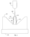
- FIG. 1 One example of cutting a sample from a bulk material is shown in FIG. 1 .
- the bulk sample material 108 is loaded into sample stage 106 of the tool.
- the stage 106 may provide a plurality of motion axes, including translation, rotation, and tilting such that an optimal orientation of the sample may be achieved at each step of the lamella formation process.
- An FIB column 102 is shown in an orientation for performing initial milling on a bulk sample material to create a sample lamella for S/TEM analysis.
- substrate 108 is oriented so that its top surface is perpendicular to focused ion beam 104 emitted from FIB column 102.
- a protective or capping layer 107 is deposited over the region of interest, for example, by beam-induced deposition of platinum, tungsten, or silicon dioxide, to protect the region of interest and to reduce ion milling artifacts.
- a protective capping layer could be deposited on the surface of the sample prior to loading the sample into the focused ion beam system. Most of the coarse ion beam machining done to create lamella 110 is performed with substrate 108 and FIB column 102 in this orientation.
- lamella 110 Due to the focusing (i.e., a convergent conical shape) and the path of ion beam 104, this perpendicular milling causes lamella 110 to be tapered from top to bottom. That is, lamella 110 is thinner at the top than it is at the bottom. In this embodiment lamella 110 remains securely attached to substrate 108 at boundary 114. For the case where lamella 110 is formed in a substrate larger than a few tens of micrometers in width or length, the lamella 110 must be removed from substrate 108 and thinned to electron transparency before it can be used in the S/TEM.
- material removed from substrate 108 while milling with ion beam 104 in the vertical orientation may be re-deposited onto the face of lamella 110, forming an undesirable layer 112 of foreign material.
- the use of a high-energy focused ion beam to form a lamella in the substrate results in a thin intermixed layer of elements 111 at the FIB milled-surface materials and the species used for ion milling, typically gallium, argon, or xenon.
- the presence of layers 111 and 112 reduces the quality of the S/TEM analysis and must be removed or polished away before lamella 110 can be used with the S/TEM.
- the FIB system may be repositioned in a tilted orientation for post-processing a sample lamella using over-tilting, polishing, and/or undercutting.
- Over-tilting is the process of removing the taper from the sides of lamella 110 to make the faces of lamella 110 substantially parallel.
- Polishing is the process of removing amorphous layer(s) 111 and 112 from lamella 110 that accumulated on lamella 110 from the previous initial milling.
- Undercutting is the process of partially or fully detaching lamella 110 from substrate 108 at or near boundary 114. Either sample stage 106 or FIB column 102 is rotated an angle 116 about the long axis of lamella 110.
- sample stage 106 or FIB column 102 is rotated an angle 116 relative to a plane defined by the long axis of lamella 110 and the normal to the top surface of substrate 108.
- sample stage 106 or FIB column 102 is rotated about an axis that is perpendicular to the sheet of FIG. 1 and located within the cross-section of lamella 110 shown in FIG. 1 , preferably near the center of the cross-section of lamella 110.
- the lamella 120 containing the ROI 122 is then relocated to a mechanical mount 124 that is compatible with both S/TEM and APM systems.
- the lamella 120 is transferred using a motorized micromanipulator and attached to the mount using an ion or electron beam-induced deposition process, or using a mechanical mechanism, or adhesive material, in a known manner.
- the lamella 120 may be arbitrarily orientated on the mount 124. The orientation is chosen to provide the desired viewing in the S/TEM and in the APT. For example, as seen in Fig.
- the lamella 120 is shown with the ROI 122 positioned on the mount 124 in a "normal" orientation, that is, with the top surface 126 of the lamella in a substantially horizontal orientation.
- the lamella 120 may be placed on the mount 124 with the ROI 122 in a "90-degree flipped" orientation in which the original top surface 126 of the lamella 120 is rotated into a substantially vertical position as seen in Fig. 2B .
- Fig. 2C Another option is seen in Fig. 2C , in which the lamella 120 is shown with the ROI 122 mounted in an "inverted" orientation relative to the orientation of the lamella as it was extracted from in the original bulk material.
- the lamella 120 is then shaped on the mount through a series of FIB milling patterns to be as thin as possible. Ideally, the lamella 120 is shaped so that the sidewalls 130 are uniformly perpendicular and the lamella 120 is formed as thin as possible to ensure an unobstructed view of the ROI 122 during analysis using the S/TEM.
- the finished lamella 120 is very thin and may have a thickness of less than 100 nm. In some embodiments, the lamella 120 may have a thickness of less than 15 nm.
- the thickness of the viewing area of the lamella containing the ROI 122 varies by less than 25%, more preferably by less than 10%, and even more preferably by less than about 3% over the viewing area.
- the lamella 120 may be formed by any known conventional technique, including but not limited to mechanical shaping, and broad beam ion milling, in addition to the aforementioned focused ion beam milling methods. Examples include U.S. Pub. No. 2013/0319849 to Fuller et al for "Preparation of Lamellae for TEM Viewing," assigned to the assignee of the present invention, U.S. Pub. No.
- the lamella 120 and mount 124 may be put through a cleaning process.
- the S/TEM study can include, for example, forming a single S/TEM image, EELS, EDS, electron holography, differential phase contrast, phase-plate contrast enhancement, and electron diffraction analyses. Heating, cooling, and even environmental exposure may be part of the S/TEM data acquisition methodology.
- S/TEM tomography using any appropriate S/TEM technique, or combinations thereof may be used as part of the correlation with APM data.
- the cleaning process may be any known series of photon, plasma, gas, or liquid cleans to remove organic surface contamination, such as, for example, carbon, or etchants to selectively remove or reshape specific materials contained within the ROI.
- the lamella 120 and mount 124 is placed within a suitable deposition system, such as, for example, a SEM with an electron or ion beam induced deposition system, a FIB with an ultra-low kV column and a suitable ion source, PVD, or CVD.
- a suitable deposition system such as, for example, a SEM with an electron or ion beam induced deposition system, a FIB with an ultra-low kV column and a suitable ion source, PVD, or CVD.
- the lamella 120 is uniformly coated with a selected material 132 as seen in FIG. 3 .
- the coating material 132 is preferably selected to compliment the field evaporation property of the elemental components within the ROI 122.
- the coating material 132 may have a mass that is different from the mass of the ROI 122 making it easier to separate data of the coating material 132 from data of the sample 120 in the APM.
- the coating material 132 is preferably relatively pure, fine grained and conformal such that gaps and voids may be filled and adherent such that an intimately bonded coating on the surface of the lamella is formed, as well as possible to deposit at relatively low temperatures.
- suitable coating materials include CVD and PVD silicon, and PVD nickel, cobalt, and chrome.
- FIGS. 4 and 5 show the lamella 120 with a hypothetical needle tip shape shown in dashed lines for the understanding of the position of the ROI 122 within the tip of the needle-shaped sample. In most cases, it will be advantageous for the embedded part of the lamella to be nominally positioned along the diameter of the cone.
- Figure 5 shows a stylized needle-shaped sample 134 with an exaggerated tip 136 for ease of understanding of location and position of the ROI 122 in the tip 136. However, it should be understood that the tip 136 is formed as more of a cone shape.
- Any preferred FIB mill process may be utilized to form the needle-shaped sample.
- One example is shown and disclosed in U.S. Pat. No. 7,442,924 to Giannuzzi et al for "Repetitive Circumferential Milling for Sample Preparation,” assigned to the assignee of the present invention, which is fully incorporated herein by reference.
- Figures 6 and 7 show a needle-shaped reconstructed APM data set 137 with the reconstructed ROI 133 in different orientations.
- Figure 6 shows a needle-shaped APM data set 137 formed with the reconstructed ROI 133 in the "normal" orientation as discussed above and shown in Fig. 2A . In this normal orientation the reconstructed ROI 133 starts well below the reconstructed capping layer 138 at the top of the data set and extends from the left of the data set to the right of the data set, nominally perpendicular to the long-axis of the conic shaped reconstructed data set 137.
- Figure 7 shows a needle-shaped reconstructed data set 137 formed with the reconstructed ROI 133 in the "90-degree" orientation as discussed above and shown in Fig.
- the reconstructed ROI 133 starts at the top of the data set and extends down into the bottom of the reconstructed data set 137, running parallel to the long-axis of the cone.
- the ROI structure 122 is buried in the bulk of the tip 136 preferably at a distance from the apex of the physical tip 136 between about 30 nm and 2 micrometers. Coating the ROI 122 with a selected material 132 provides a more uniform electric field over a larger extent of the needle tip 136 than would be achieved if the ROI were formed in a needle tip formed from the bulk sample material. The time- and position-variable electric field is then largely confined to the thin ribbon of inhomogeneous material in the embedded lamella.
- an "embedded-lamella" APM specimen is more "malleable” than needle samples formed in a bulk specimen because the reduced area of complex tip shaping allows more controlled field evaporation and fewer field evaporation artifacts such as micro-fractures, and cluster and uncorrelated evaporation events.
- the needle-shaped sample 136 is analyzed and reconstructed in the APM and the digitized microstructure is visualized and merged or correlated with the S/TEM data using separate software tools.
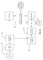
- FIG 8 shows a flow chart of the process of forming the needle-shaped sample of this invention.
- the ROI is identified and isolated, or marked, as necessary in step 140.
- a lamella for the S/TEM is formed in step 142.
- the lamella sample is then studied with the S/TEM in step 144, which can include 3D and ultrahigh resolution (UHR) S/TEM.
- the lamella sample is cleaned and coated or embedded within the coating apparatus in step 146.
- the sample is then subjected to the FIB milling process to form the needle-shaped sample in step 148.
- the needle-shaped sample is studied with the APM in step 152 or iteratively studied in both APM and S/TEM 154 by moving the sample back and forth between the two instruments.
- the data obtained from the S/TEM and APM is then correlated using separate software tools in step 155 and the correlated structural and elemental data and images are displayed in step 157.
- Figure 9 shows variations anticipated within each of the steps of the generic workflow shown in Figure 8
- a sample for analysis on an atomic probe microscope comprises a first layer having a thickness of less than 100 nm and containing a region of interest; a second layer attached to the first layer; characterized in that the second layer has a field evaporation property that compliments the elemental components within the region of interest; and the sample is needle-shaped having a substantially sharp conical tip.
- the region of interest is contained in the sharp conical tip of the needle-shaped sample.
- a method of analyzing a sample comprises forming a lamella using a focused ion beam, the lamella having a thickness of less than 200 nm and including a region of interest; positioning the lamella onto a mount compatible with both S/TEM and APM systems; depositing material onto the lamella to embed with the region of interest; and forming a sample from the lamella; characterized in that the sample is needle-shaped, the needle shaped sample having a conical tip that includes the region of interest.
- the lamella has a top surface and is positioned on the mount in an orientation with the top surface substantially horizontal. In some embodiments, the lamella has a top surface and is positioned on the mount in an orientation with the top surface substantially vertical. In some embodiments, the lamella has a top surface and is positioned on the mount in an inverted orientation with the top surface connected to the mount.
- the deposited material has a mass that is different from the mass of the region of interest.
- the deposited material is any one of silicon, nickel, cobalt, and chrome.
- the region of interest is located between 30 nm and 2 micrometers from the apex of the tip.
- the method further comprises forming an image of the region of interest using a transmission electron microscope before depositing material onto the lamella.
- imaging the region of interest in the lamella using transmission electron microscope includes forming images of the sample at different angles relative to the electron beam to form a three dimensional image of the region of interest by tomography.
- the method further comprises forming an image of the region of interest using atomic probe microscopy after forming a needle-shaped sample from the lamella.
- forming images of the region of interest using atomic probe microscopy includes forming multiple images of the needle shaped sample at different depths.
- the method further comprises forming an image of the region of interest using a transmission electron microscope before depositing material onto the lamella; forming an image of the region of interest using atomic probe microscopy after forming a needle-shaped sample from the lamella; and combining on a display information derived from the transmission electron microscope and information derived from the atomic probe microscope.
- depositing material onto the lamella includes depositing a material having a field evaporation property that compliments the elemental components within the region of interest.
Landscapes
- Physics & Mathematics (AREA)
- Health & Medical Sciences (AREA)
- General Health & Medical Sciences (AREA)
- General Physics & Mathematics (AREA)
- Analytical Chemistry (AREA)
- Chemical & Material Sciences (AREA)
- Life Sciences & Earth Sciences (AREA)
- Biochemistry (AREA)
- Immunology (AREA)
- Pathology (AREA)
- Radiology & Medical Imaging (AREA)
- Nuclear Medicine, Radiotherapy & Molecular Imaging (AREA)
- Sampling And Sample Adjustment (AREA)
- Analysing Materials By The Use Of Radiation (AREA)
- Other Investigation Or Analysis Of Materials By Electrical Means (AREA)
Priority Applications (1)
| Application Number | Priority Date | Filing Date | Title |
|---|---|---|---|
| EP15157492.8A EP2916343B1 (de) | 2014-03-05 | 2015-03-04 | Herstellung einer Lamelle zur korrelativen tomografischen Analyse mit atomarer Auflösung |
Applications Claiming Priority (1)
| Application Number | Priority Date | Filing Date | Title |
|---|---|---|---|
| US201461948516P | 2014-03-05 | 2014-03-05 |
Publications (1)
| Publication Number | Publication Date |
|---|---|
| EP2916342A1 true EP2916342A1 (de) | 2015-09-09 |
Family
ID=50771107
Family Applications (2)
| Application Number | Title | Priority Date | Filing Date |
|---|---|---|---|
| EP14169243.4A Withdrawn EP2916342A1 (de) | 2014-03-05 | 2014-05-21 | Herstellung einer Lamelle zur korrelativen tomografischen Analyse mit atomarer Auflösung |
| EP15157492.8A Active EP2916343B1 (de) | 2014-03-05 | 2015-03-04 | Herstellung einer Lamelle zur korrelativen tomografischen Analyse mit atomarer Auflösung |
Family Applications After (1)
| Application Number | Title | Priority Date | Filing Date |
|---|---|---|---|
| EP15157492.8A Active EP2916343B1 (de) | 2014-03-05 | 2015-03-04 | Herstellung einer Lamelle zur korrelativen tomografischen Analyse mit atomarer Auflösung |
Country Status (4)
| Country | Link |
|---|---|
| US (1) | US9797923B2 (de) |
| EP (2) | EP2916342A1 (de) |
| JP (1) | JP6700664B2 (de) |
| CN (1) | CN104897696B (de) |
Families Citing this family (13)
| Publication number | Priority date | Publication date | Assignee | Title |
|---|---|---|---|---|
| US9761408B2 (en) * | 2015-02-24 | 2017-09-12 | Fei Company | Pattern matching using a lamella of known shape for automated S/TEM acquisition and metrology |
| US9627176B2 (en) | 2015-07-23 | 2017-04-18 | Fei Company | Fiducial formation for TEM/STEM tomography tilt-series acquisition and alignment |
| US9978586B2 (en) * | 2015-11-06 | 2018-05-22 | Fei Company | Method of material deposition |
| US20180122652A1 (en) * | 2016-11-03 | 2018-05-03 | Qualcomm Incorporated | Method of ROI Encapsulation During Axis Conversion of Cross-Sectional TEM Lamellae |
| US9905394B1 (en) * | 2017-02-16 | 2018-02-27 | Carl Zeiss Microscopy Gmbh | Method for analyzing an object and a charged particle beam device for carrying out this method |
| JP6646002B2 (ja) * | 2017-03-22 | 2020-02-14 | 富士フイルム株式会社 | 放射線検出器及び放射線画像撮影装置 |
| CN109521080A (zh) * | 2017-09-19 | 2019-03-26 | 台湾积体电路制造股份有限公司 | 分析试片及其制备方法与材料分析的方法 |
| EP3518270A1 (de) * | 2018-01-25 | 2019-07-31 | FEI Company | Innovative abbildungstechnik in der transmissionsladungsteilchenmikroskopie |
| CN111829841A (zh) * | 2019-04-15 | 2020-10-27 | 台湾积体电路制造股份有限公司 | 针状样品、针状样品的分析以及制备方法 |
| CN111220819B (zh) * | 2020-01-19 | 2022-03-25 | 中国科学院上海微系统与信息技术研究所 | 一种聚焦离子束切割制样方法 |
| US11837435B2 (en) * | 2020-08-19 | 2023-12-05 | Taiwan Semiconductor Manufacturing Co., Ltd. | Atom probe tomography specimen preparation |
| CN112146953B (zh) * | 2020-09-21 | 2024-03-01 | 长江存储科技有限责任公司 | 测试样品及其制备方法 |
| US11476079B1 (en) | 2021-03-31 | 2022-10-18 | Fei Company | Method and system for imaging a multi-pillar sample |
Citations (7)
| Publication number | Priority date | Publication date | Assignee | Title |
|---|---|---|---|---|
| JP2005233786A (ja) * | 2004-02-19 | 2005-09-02 | Toshiba Corp | 局所分析用針状試料,試料ホルダ組立体,局所分析装置,及び局所分析用針状試料の作製方法 |
| WO2007075908A2 (en) * | 2005-12-23 | 2007-07-05 | Imago Scientific Instruments Corporation | Atom probe test standards and associated methods |
| US7442924B2 (en) | 2005-02-23 | 2008-10-28 | Fei, Company | Repetitive circumferential milling for sample preparation |
| JP2010243458A (ja) * | 2009-04-10 | 2010-10-28 | Fujitsu Ltd | 3次元アトムプローブ構造データ解析方法 |
| WO2012103534A1 (en) | 2011-01-28 | 2012-08-02 | Fei Company | Tem sample preparation |
| US20130248354A1 (en) | 2011-12-01 | 2013-09-26 | Fei Company | High Throughput TEM Preparation Processes and Hardware for Backside Thinning of Cross-Sectional View Lamella |
| US20130319849A1 (en) | 2012-05-21 | 2013-12-05 | Fei Company | Preparation of lamellae for tem viewing |
Family Cites Families (18)
| Publication number | Priority date | Publication date | Assignee | Title |
|---|---|---|---|---|
| JP3976599B2 (ja) * | 2002-03-27 | 2007-09-19 | 独立行政法人科学技術振興機構 | 耐高温腐食性、耐酸化性に優れた耐熱性Ti合金材料およびその製造方法 |
| WO2004013603A2 (en) * | 2002-08-05 | 2004-02-12 | California Institute Of Technology | A method of sample preparation for atom probes and source of specimens |
| JP2005019218A (ja) * | 2003-06-26 | 2005-01-20 | Jeol Ltd | 電子顕微鏡装置 |
| JP4464223B2 (ja) * | 2004-08-10 | 2010-05-19 | 富士通株式会社 | ナノレベル構造組成評価用試料、その製造方法、及び、ナノレベル構造組成評価方法 |
| WO2008057066A2 (en) * | 2005-07-28 | 2008-05-15 | Imago Scientific Instruments Corporation | Specimens for microanalysis processes |
| US7884323B2 (en) * | 2005-08-16 | 2011-02-08 | Cameca Instruments, Inc. | Atom probes, atom probe specimens, and associated methods |
| JP4947965B2 (ja) * | 2005-12-06 | 2012-06-06 | ラピスセミコンダクタ株式会社 | 透過型電子顕微鏡用の試料の作製方法、観察方法及び構造 |
| JP2008157673A (ja) * | 2006-12-21 | 2008-07-10 | Sii Nanotechnology Inc | 試料把持体の把持面作製方法 |
| US8670608B2 (en) * | 2008-06-20 | 2014-03-11 | Cameca Instruments, Inc. | 3D atomic scale imaging methods |
| JP5281525B2 (ja) * | 2009-09-11 | 2013-09-04 | 一般財団法人電力中央研究所 | 試料作製方法 |
| JP2012073242A (ja) * | 2010-09-23 | 2012-04-12 | Imec | レーザーアトムプローブおよびレーザーアトムプローブ分析方法 |
| US8604446B2 (en) * | 2011-08-08 | 2013-12-10 | The State Of Oregon Acting By And Through The State Board Of Higher Education On Behalf Of The University Of Oregon | Devices and methods for cryo lift-out with in situ probe |
| US8740209B2 (en) * | 2012-02-22 | 2014-06-03 | Expresslo Llc | Method and apparatus for ex-situ lift-out specimen preparation |
| US9733164B2 (en) | 2012-06-11 | 2017-08-15 | Fei Company | Lamella creation method and device using fixed-angle beam and rotating sample stage |
| EP2708874A1 (de) | 2012-09-12 | 2014-03-19 | Fei Company | Verfahren zur Durchführung von Tomographiebildgebung einer Probe in einem Mikroskop mit geladenen Teilchen |
| EP2738786A1 (de) | 2012-11-29 | 2014-06-04 | Fei Company | Verfahren zur Durchführung von Tomographiebildgebung einer Probe in einem Ladungsträger-Mikroskop |
| US9287104B2 (en) * | 2013-08-14 | 2016-03-15 | Kabushiki Kaisha Toshiba | Material inspection apparatus and material inspection method |
| JP6382495B2 (ja) * | 2013-09-02 | 2018-08-29 | 株式会社日立ハイテクサイエンス | 荷電粒子ビーム装置 |
-
2014
- 2014-05-21 EP EP14169243.4A patent/EP2916342A1/de not_active Withdrawn
-
2015
- 2015-02-20 US US14/627,770 patent/US9797923B2/en active Active
- 2015-03-04 EP EP15157492.8A patent/EP2916343B1/de active Active
- 2015-03-04 JP JP2015042328A patent/JP6700664B2/ja active Active
- 2015-03-04 CN CN201510161299.3A patent/CN104897696B/zh active Active
Patent Citations (7)
| Publication number | Priority date | Publication date | Assignee | Title |
|---|---|---|---|---|
| JP2005233786A (ja) * | 2004-02-19 | 2005-09-02 | Toshiba Corp | 局所分析用針状試料,試料ホルダ組立体,局所分析装置,及び局所分析用針状試料の作製方法 |
| US7442924B2 (en) | 2005-02-23 | 2008-10-28 | Fei, Company | Repetitive circumferential milling for sample preparation |
| WO2007075908A2 (en) * | 2005-12-23 | 2007-07-05 | Imago Scientific Instruments Corporation | Atom probe test standards and associated methods |
| JP2010243458A (ja) * | 2009-04-10 | 2010-10-28 | Fujitsu Ltd | 3次元アトムプローブ構造データ解析方法 |
| WO2012103534A1 (en) | 2011-01-28 | 2012-08-02 | Fei Company | Tem sample preparation |
| US20130248354A1 (en) | 2011-12-01 | 2013-09-26 | Fei Company | High Throughput TEM Preparation Processes and Hardware for Backside Thinning of Cross-Sectional View Lamella |
| US20130319849A1 (en) | 2012-05-21 | 2013-12-05 | Fei Company | Preparation of lamellae for tem viewing |
Non-Patent Citations (1)
| Title |
|---|
| LARSON ET AL.: "Atom probe tomography spatial reconstruction: Status and directions", CURRENT OPINION IN SOLID STATE AND MATERIALS SCIENCE, vol. 17, 2013, pages 236 - 247, XP055146572, DOI: doi:10.1016/j.cossms.2013.09.002 |
Also Published As
| Publication number | Publication date |
|---|---|
| JP2015170600A (ja) | 2015-09-28 |
| JP6700664B2 (ja) | 2020-05-27 |
| US9797923B2 (en) | 2017-10-24 |
| CN104897696B (zh) | 2020-08-21 |
| US20150253353A1 (en) | 2015-09-10 |
| EP2916343A1 (de) | 2015-09-09 |
| EP2916343B1 (de) | 2017-07-05 |
| CN104897696A (zh) | 2015-09-09 |
Similar Documents
| Publication | Publication Date | Title |
|---|---|---|
| US9797923B2 (en) | Fabrication of a malleable lamella for correlative atomic-resolution tomographic analyses | |
| Munroe | The application of focused ion beam microscopy in the material sciences | |
| Larson et al. | Local electrode atom probe tomography | |
| US8878147B2 (en) | Method and apparatus for in situ preparation of serial planar surfaces for microscopy | |
| Weyland et al. | Extending energy-filtered transmission electron microscopy (EFTEM) into three dimensions using electron tomography | |
| CN109256312B (zh) | 用于原位制备显微镜样本的方法 | |
| JP6974820B2 (ja) | 荷電粒子ビーム装置、試料加工方法 | |
| Kelly | Atomic-scale analytical tomography | |
| US7180061B2 (en) | Method for electron beam-initiated coating for application of transmission electron microscopy | |
| Pérez-Willard et al. | Focused ion beam preparation of atom probe specimens containing a single crystallographically well-defined grain boundary | |
| Blavette et al. | Early developments and basic concepts | |
| Larson et al. | Microstructural investigations in metals using atom probe tomography with a novel specimen-electrode geometry | |
| Berger et al. | A novel method for specimen preparation and analysis of CVD diamond coated tools using focussed ion beams (FIB) and scanning electron microscopy (SEM) | |
| Patzig et al. | Microstructure analysis of glasses and glass ceramics | |
| Brodu et al. | A new and unexpected spatial relationship between interaction volume and diffraction pattern in electron microscopy in transmission | |
| JP7214262B2 (ja) | 荷電粒子ビーム装置、試料加工方法 | |
| Goldstein et al. | Focused Ion Beam Applications in the SEM Laboratory | |
| JP4316400B2 (ja) | 表面層評価方法 | |
| US11227742B1 (en) | Electron microscopic specimen, and methods for preparing and performing microscopic examination of the same | |
| Adams et al. | Electron-based imaging techniques | |
| Larson et al. | Specimen preparation | |
| Pearmain | Electron microscopy characterisation of size-selected Pd clusters and industrial Pd catalysts | |
| Bobynko | Characterisation and absolute quantification of nanosized V and Nb precipitates in high manganese steel using DualEELS | |
| Adams et al. | Spatially confined analysis | |
| Audinot et al. | Combined SIMS and AFM study of complex structures of streamers on metallic multilayers |
Legal Events
| Date | Code | Title | Description |
|---|---|---|---|
| PUAI | Public reference made under article 153(3) epc to a published international application that has entered the european phase |
Free format text: ORIGINAL CODE: 0009012 |
|
| AK | Designated contracting states |
Kind code of ref document: A1 Designated state(s): AL AT BE BG CH CY CZ DE DK EE ES FI FR GB GR HR HU IE IS IT LI LT LU LV MC MK MT NL NO PL PT RO RS SE SI SK SM TR |
|
| AX | Request for extension of the european patent |
Extension state: BA ME |
|
| STAA | Information on the status of an ep patent application or granted ep patent |
Free format text: STATUS: THE APPLICATION IS DEEMED TO BE WITHDRAWN |
|
| 18D | Application deemed to be withdrawn |
Effective date: 20160310 |