EP3111476B1 - Verbesserte scheibenzelle für mehrere druckkontaktierte halbleiterbauelemente - Google Patents
Verbesserte scheibenzelle für mehrere druckkontaktierte halbleiterbauelemente Download PDFInfo
- Publication number
- EP3111476B1 EP3111476B1 EP15706201.9A EP15706201A EP3111476B1 EP 3111476 B1 EP3111476 B1 EP 3111476B1 EP 15706201 A EP15706201 A EP 15706201A EP 3111476 B1 EP3111476 B1 EP 3111476B1
- Authority
- EP
- European Patent Office
- Prior art keywords
- semiconductor
- shaped casing
- disc shaped
- semiconductor component
- semiconductor components
- Prior art date
- Legal status (The legal status is an assumption and is not a legal conclusion. Google has not performed a legal analysis and makes no representation as to the accuracy of the status listed.)
- Active
Links
Images


Classifications
-
- H—ELECTRICITY
- H10—SEMICONDUCTOR DEVICES; ELECTRIC SOLID-STATE DEVICES NOT OTHERWISE PROVIDED FOR
- H10W—GENERIC PACKAGES, INTERCONNECTIONS, CONNECTORS OR OTHER CONSTRUCTIONAL DETAILS OF DEVICES COVERED BY CLASS H10
- H10W40/00—Arrangements for thermal protection or thermal control
- H10W40/20—Arrangements for cooling
- H10W40/22—Arrangements for cooling characterised by their shape, e.g. having conical or cylindrical projections
-
- H—ELECTRICITY
- H10—SEMICONDUCTOR DEVICES; ELECTRIC SOLID-STATE DEVICES NOT OTHERWISE PROVIDED FOR
- H10W—GENERIC PACKAGES, INTERCONNECTIONS, CONNECTORS OR OTHER CONSTRUCTIONAL DETAILS OF DEVICES COVERED BY CLASS H10
- H10W40/00—Arrangements for thermal protection or thermal control
- H10W40/40—Arrangements for thermal protection or thermal control involving heat exchange by flowing fluids
- H10W40/47—Arrangements for thermal protection or thermal control involving heat exchange by flowing fluids by flowing liquids, e.g. forced water cooling
-
- H—ELECTRICITY
- H10—SEMICONDUCTOR DEVICES; ELECTRIC SOLID-STATE DEVICES NOT OTHERWISE PROVIDED FOR
- H10W—GENERIC PACKAGES, INTERCONNECTIONS, CONNECTORS OR OTHER CONSTRUCTIONAL DETAILS OF DEVICES COVERED BY CLASS H10
- H10W40/00—Arrangements for thermal protection or thermal control
- H10W40/60—Securing means for detachable heating or cooling arrangements, e.g. clamps
- H10W40/611—Bolts or screws
-
- H—ELECTRICITY
- H10—SEMICONDUCTOR DEVICES; ELECTRIC SOLID-STATE DEVICES NOT OTHERWISE PROVIDED FOR
- H10W—GENERIC PACKAGES, INTERCONNECTIONS, CONNECTORS OR OTHER CONSTRUCTIONAL DETAILS OF DEVICES COVERED BY CLASS H10
- H10W72/00—Interconnections or connectors in packages
-
- H—ELECTRICITY
- H10—SEMICONDUCTOR DEVICES; ELECTRIC SOLID-STATE DEVICES NOT OTHERWISE PROVIDED FOR
- H10W—GENERIC PACKAGES, INTERCONNECTIONS, CONNECTORS OR OTHER CONSTRUCTIONAL DETAILS OF DEVICES COVERED BY CLASS H10
- H10W76/00—Containers; Fillings or auxiliary members therefor; Seals
- H10W76/10—Containers or parts thereof
- H10W76/12—Containers or parts thereof characterised by their shape
- H10W76/13—Containers comprising a conductive base serving as an interconnection
- H10W76/138—Containers comprising a conductive base serving as an interconnection having another interconnection being formed by a cover plate parallel to the conductive base, e.g. sandwich type
-
- H—ELECTRICITY
- H10—SEMICONDUCTOR DEVICES; ELECTRIC SOLID-STATE DEVICES NOT OTHERWISE PROVIDED FOR
- H10W—GENERIC PACKAGES, INTERCONNECTIONS, CONNECTORS OR OTHER CONSTRUCTIONAL DETAILS OF DEVICES COVERED BY CLASS H10
- H10W78/00—Detachable holders for supporting packaged chips in operation
-
- H—ELECTRICITY
- H10—SEMICONDUCTOR DEVICES; ELECTRIC SOLID-STATE DEVICES NOT OTHERWISE PROVIDED FOR
- H10W—GENERIC PACKAGES, INTERCONNECTIONS, CONNECTORS OR OTHER CONSTRUCTIONAL DETAILS OF DEVICES COVERED BY CLASS H10
- H10W90/00—Package configurations
Definitions
- the present invention relates to a disk cell for a plurality of semiconductor components, in particular a plurality of power semiconductor components.
- such disc cells are used for receiving and electrically contacting at least one semiconductor component and are generally in heat-conducting contact with a heat sink.
- the essential meaning of this disk cell is the hermetic closure of the semiconductor component with simultaneous electrical and thermal connection by pressure contacting of the semiconductor component from the outside.
- the known disk cell essentially comprises a housing and at least one semiconductor component.
- the disk cell represents a tradeable unit.
- disk cells are known in which a plurality of semiconductor components, which have the same design with respect to their geometric dimensions, are included. This is unproblematic insofar as the components are identical with respect to their mechanical load limits in the case of matching design.
- the problem is the clamping of several components then, if they are, for example, due to different geometry mechanically different loads. While the pure placement of the housing interior with the semiconductor components is usually unproblematic, the mechanically weakest component can easily be damaged during clamping, when the disk cell is usually clamped at the end user for electrical and thermal contact. Due to the different load limits so far had the semiconductor devices of different types are clamped in separate disc cells in order to adjust the clamping separately for each component, so as ultimately to be able to take into account the different mechanical load limits of the components. This has the disadvantage that the number of components is increased, the construction volume of the disk cell disadvantageous large fails and the construction and / or the possibly necessary specific adjustment of the clamping is relatively complex.
- the disc cell comprehensive arrangements have to clamping means, such as compression or compression fittings, which serve the definition of the semiconductor devices and the electrical and thermal pressure contact of the invention according to several semiconductor devices.
- clamping means such as compression or compression fittings
- high-voltage-resistant semiconductor components are high-voltage thyristors, which are the central components in high-performance converters.
- High requirements apply to the reliability of the components. Since the components have comparatively brittle layers of semiconductor material, the components are always exposed to the risk of being destroyed in the event of mechanical overstressing due to the pressure contact.
- the present invention has the object to provide a disk cell for a plurality of semiconductor devices and an arrangement thereof with clamping means, in which a high integration density is achieved despite different semiconductor devices, the number of components but also the number of disk cells required is reduced, the volume of construction is reduced, simplifies the setting of the clamping and / or the different mechanical load limits of the components can be better accommodated.
- This object is achieved by a disc cell with the features of claim 1.
- particularly advantageous embodiments of the invention disclose the dependent claims. It should be noted that the features listed individually in the claims can be combined with each other in any technically meaningful manner and show further embodiments of the invention. The description additionally characterizes and specifies the invention, in particular in connection with the figures.
- the invention relates to a disk cell for a plurality of semiconductor devices as described in claim 1.
- the disc cell according to the invention comprises a housing.
- the housing preferably has a wall made of an electrically non-conductive material, such as ceramic.
- the wall is, for example, annular.
- the semiconductor components are preferably hermetically enclosed in the housing interior.
- the disk cell comprises at least a first semiconductor device of the first type accommodated in the housing and at least one second semiconductor device of the second design accommodated in the housing.
- the term "disc cell” thus defines a unit of one housing and several Semiconductor devices, which are also referred to below as "components".
- the components are captively received in the housing, even if the disc cell is not clamped and / or attached to a heat sink.
- different design is to be interpreted broadly, and means, for example, different outer dimensions and / or geometries, but also a difference in the layer structure, with otherwise identical outer dimensions, but may also include a different contact force in the pressure contact. It is preferably at least a difference in the mechanical load limit of the various types parallel to the direction of the clamping.
- the housing comprises at least one metallic pressure plate which engages over the first and second semiconductor components and is aligned essentially at right angles to the clamping force, for clamping the first and second semiconductor components.
- the pressure plate is designed so that the clamping force acts locally limited to these to clamp on the pressure plate, the first and second semiconductor device, wherein the first semiconductor device is disposed below the local Einwirk Scheme the clamping force and the second component at least partially, i. partially to completely, preferably completely, outside the local area of action is arranged.
- the invention further relates to an arrangement of the previously described disc cell and clamping means, which are provided to clamp the first and second semiconductor device under the action of a clamping force generated by the clamping means and to electrically contact the first and second semiconductor device.
- the clamping force is generated for example by springs or screw, preferably by a pull or compression fitting.
- the components of the first and second types are clamped between a previously described pressure plate and a pressure-receiving counter-plate, wherein the counter-plate, for example, bears against the entire surface of a heat sink.
- the components of the first and second type are clamped between two printing plates designed according to the invention.
- the pressure plate and the counter-plate are designed or height compensation discs are provided that takes place at the same time before clamping of the counter-plate and pressure plate touching contact with the first semiconductor device and the second semiconductor device at the same time.
- the projection of the pressure plate over the Einwirk Symposium also ensures a splitting of the force curve. While the first semiconductor device in the force curve the clamping force is arranged, the second arranged under the protruding part of the pressure plate semiconductor device sits in the diverted via the pressure plate force curve.
- the metallic, preferably round pressure plate thus acts as an elastic bending beam and cushions the action on the second semiconductor component (s).
- the contact pressure and thus also the mechanical stress of the second semiconductor component (s) is thus reduced compared to the first semiconductor component (s). This can be used, for example, to arrange that semiconductor component which has a less critical dependence of the contact resistance on the clamping force as the second semiconductor component in the branched force profile.
- the second semiconductor component preferably has a design whose mechanical load limit in the direction of the clamping is lower than the corresponding one of the first semiconductor component. This is inventively in the region of the branched force curve.
- the different load limit between the first and second components results from a different thickness of the semiconductor layer, which is generally oriented at right angles to the clamping force. Due to the inventive design of the disc cell a "sprung" stress of the second component is ensured even at maximum clamping of the first component and it can be ensured in spite of maximum stress by the clamping force of the first component lower stress on the second component. Thus, it is possible to pair mechanically less resilient components with higher-load components in a disc cell.
- the pressure plate is applied to the corresponding contacting surfaces of the semiconductor components and thus simultaneously serves the direct electrical and thermal contacting of the semiconductor components.
- the first semiconductor component does not rest completely over at least one of its contact surfaces, at least in the unconstrained state.
- it forms the semiconductor device with its adjacent counterpart, for example, the pressure plate according to the invention or the pressure-receiving counter-plate from a cavity.
- the first semiconductor component it is possible for the first semiconductor component to undergo a change in shape under the effect of the clamping subject and the plant of the semiconductor device increases by elastic or plastic deformation of the device with increasing clamping force.
- the semiconductor device "cushions" the clamping.
- the clamping of the second semiconductor device can be better adjusted due to the opposing force of the first semiconductor device.
- This is preferably achieved by a curved contact surface on the side of the semiconductor component.
- an outer layer of the first semiconductor device made of semiconductor material, for example silicon has a surface that is curved away from the contact surface.
- the first semiconductor component that is to say for example the entire layer structure, is curved in the unconstrained state.
- the maximum clear distance between the contact surface and the associated mating surface in the unclamped state is in a range of 5 .mu.m to 150 .mu.m, preferably 10 .mu.m to 100 .mu.m.
- the term clear distance means the maximum possible height difference between full-surface concern and unloaded concern.
- the outer circumference of the first semiconductor component is outside the Einwirk Kunststoffs the clamping force or is congruent with the outer circumference of the Einwirk Kunststoffs.
- a high compliance of the first semiconductor component is achieved in the case of plate-shaped semiconductor components.
- the disk cell according to the invention exactly one first semiconductor device is provided, while a plurality of second semiconductor devices are provided and the second semiconductor devices at a consistent distance or at different distances, each with a different distance to be encompassed, are arranged distributed around the first semiconductor device.
- the integration density can be increased without having to forego the benefits mentioned above, such as the mechanical stress gradation in the radial direction.
- the local area of influence of the pressure plate preferably detects its geometric center.
- the first semiconductor device is formed as a circular sheet and there are provided a plurality of second semiconductor devices, which are arranged distributed uniformly along one or more concentric circles around the radial circumference of the first semiconductor device.
- fluid-conducting channels are integrated into the pressure plate in order to be able to flow through the pressure plate for active cooling with a cooling medium.
- the first semiconductor component is designed, for example, as a round sheet. For example, it has a diameter in the range of 10 to 100 mm, preferably in the range of 20 to 80 mm, more preferably in the range of 50 to 70 mm, such as 60 mm.
- the second semiconductor devices arranged around the first semiconductor component are, for example, arranged in a ring around the first semiconductor component whose inner / outer diameter is in the range from 10/20 to 100/200 mm, preferably in the range from 20/40 to 80 / 160 mm, more preferably in the range of 50/100 to 70/140 mm, such as 60/120 mm.
- the maximum areas provided for the electrical contacting are in a specific ratio.
- the ratio of the active area of the first device to that of the second device is in a range of 1: 1 to 1: 4, more preferably in the range of 1: 1.5 to 1: 2.5, and is for example 1: 2.
- the at least one, second semiconductor component is formed as a rectangular, preferably square, or trapezoidal sheet.
- the first semiconductor device is a monolithic semiconductor device, such as a diode or thyristor.
- the at least one second semiconductor device is an insulated gate bipolar transistor (IGBT).
- IGBT insulated gate bipolar transistor
- the semiconductor components of the first and second types are preferably arranged spaced from one another in the direction perpendicular to the clamping force, for example, the distance is 2 mm to 10 mm.
- the invention further relates to an arrangement of a heat sink and a disk cell in one of the embodiments described above and with the corresponding technical advantages mentioned above.
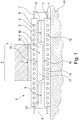
- FIG. 1 is shown in section and schematically a first arrangement of a disc cell 1 and clamping means 4, 13 according to the invention.
- the disk cell 1 has a hermetically sealed housing 2, 3, 7, 8.
- the housing 2, 3, 7, 8 comprises an electrically insulating ring 8 made of ceramic, which is provided at its end faces with a metallic coating. By means of the coating, the ring is soldered on both end faces in each case with an annular disc 7 made of copper.
- the annular discs 7 each close hermetically sealed with a pressure plate 2 and a pressure-receiving counter-plate 3 from.
- the semiconductor components 5, 6 each have semiconductor layers 10, 10 'running at right angles to the clamping direction. Furthermore, metallic layers for electrically contacting the semiconductor components 5, 6 are respectively provided on the sides of the semiconductor components 5, 6 which are in touching contact with the pressure plate 2 and the counterplate 3. The electrical contact and a required heat dissipation via the pressure plate 2 and the counter-plate 3.
- the pressure plate 2 and the counter-plate 3 with one or more fluid-conducting channels 11, 12 are traversed.
- the channels 11 of the pressure plate 2 and the channels 12 of the counter-plate 3 are arranged in an imaginary plane oriented at right angles to the clamping direction.
- the counter plate 3 is located in the FIG. 1 shown arrangement over a full area on a heat sink 13.
- the clamping means comprise a plunger 4, 18 via which a clamping force F generated, for example, by a pressure screw, not shown, acts on the round pressure plate 2.
- the contact surface 9 is defined by a plateau-shaped elevation 18 of the pressure plate 2.
- the elevation 18 may be formed integrally with the pressure plate 2 or as a separate part of the pressure plate 2.
- the second semiconductor components 5 are arranged below the outer part of the pressure plate 2 projecting beyond the action region. Due to the elastic flexibility of the Pressure plate 2 in the branched force curve through the second semiconductor devices 5 whose mechanical stress is reduced compared to that of the first semiconductor device 6. If, for example, the first 6 and second 5 semiconductor components do not have the same mechanical maximum load limits, mechanical destruction of the second semiconductor components 5 can be prevented by the design of the pressure plate 2 according to the invention until the maximum load of the first semiconductor component 6 is reached, which is sought for electrical and thermal contacting reasons ,
- FIG. 2 a second embodiment of the arrangement according to the invention is shown, which differs from the in FIG. 1 shown arrangement by the configuration of the clamping means 4, 13 and differs in that not only only one printing plate 2 according to the invention is provided, but two of these printing plates 2.
- FIG. 3 is one both the FIG. 1 as well as the FIG. 2 relevant detail shown.
- FIG. 3 shows the layer structure of the first semiconductor component 6 located between the pressure plates 2 or between the pressure plate 2 and the counterplate 3 in the non-clamped state which is merely in contact with the pressure plates 2 or the counterplate 3.
- the entire layer structure of the first component 6 is curved, the curvature shown is not shown to scale.
- the layer structure curved away from the semiconductor layer 10 and toward the metallic molybdenum layer 17 ensures a "bulging" of the semiconductor component 6 by the amount X on both sides of the first component 6 in the region of the contact surfaces 15 and 15 '. With increasing clamping thus it comes to bending the layer structure of the first component 6 against this Vorkrümmung.
- the preferably bending moment based on the pre-curvature counteracts the clamping and simplifies the adjustment and scaling of the clamping force F to the maximum load limit of the first semiconductor component 6. Thus, the risk of mechanical destruction of the second semiconductor component 5 during clamping is minimized.
Landscapes
- Cooling Or The Like Of Semiconductors Or Solid State Devices (AREA)
- Thyristors (AREA)
- Die Bonding (AREA)
Description
- Die vorliegende Erfindung betrifft eine Scheibenzelle für mehrere Halbleiterbauelemente, insbesondere mehrere Leistungshalbleiterbauelemente. Im Allgemeinen dienen solche Scheibenzellen der Aufnahme und elektrischen Kontaktierung wenigstens eines Halbleiterbauelements und stehen in der Regel in wärmeleitendem Kontakt mit einem Kühlkörper. Wesentlicher Sinn dieser Scheibenzelle ist der hermetische Verschluss des Halbleiterbauelements bei gleichzeitiger elektrischer und thermischer Verbindung durch Druckkontaktierung des Halbleiterbauelements von außen. Die bekannte Scheibenzelle umfasst im Wesentlichen ein Gehäuse und wenigstens ein Halbleiterbauelement. Die Scheibenzelle stellt dabei eine handelbare Einheit dar. Darüber hinaus sind Scheibenzellen bekannt, in der mehrere Halbleiterbauelemente, die bezüglicher ihrer geometrischen Abmessungen die gleiche Bauart aufweisen, aufgenommen sind. Dies ist insoweit unproblematisch, da bei übereinstimmender Bauart die Bauelemente bezüglich ihrer mechanischen Belastungsgrenzen identisch sind. Problematisch wird das Einspannen mehrerer Bauelemente dann, wenn diese beispielsweise schon aufgrund unterschiedlicher Geometrie mechanisch unterschiedlich belastbar sind. Während die reine Bestückung des Gehäuseinneren mit den Halbleiterbauelementen in der Regel unproblematisch ist, kann das mechanisch schwächste Bauelement beim Einspannen leicht Schaden nehmen, wenn die Scheibenzelle in der Regel beim Endabnehmer zur elektrischen und thermischen Kontaktierung eingespannt wird. Aufgrund der unterschiedlichen Belastungsgrenzen mussten daher bisher die Halbleiterbauelemente unterschiedlicher Bauart in separaten Scheibenzellen eingespannt werden, um die Einspannung für jedes Bauelement separat einstellen zu können, um damit letztlich den unterschiedlichen mechanischen Belastungsgrenzen der Bauelemente Rechnung tragen zu können. Dies hat den Nachteil, dass die Anzahl der Bauteile erhöht ist, das Bauvolumen der Scheibenzelle nachteilig groß ausfällt und die Konstruktion und/ oder die gegebenenfalls notwendige spezifische Einstellung der Einspannung vergleichsweise aufwändig ist.
- Gattungsgemäße, die Scheibenzelle umfassende Anordnungen weisen dazu Einspannmittel, wie Zug- oder Druckverschraubungen, auf, die der Festlegung der Halbleiterbauelemente und der elektrischen sowie thermischen Druckkontaktierung der erfindungsgemäß mehreren Halbleiterbauelemente dienen. Im Hinblick auf die gerade in der Leistungshalbleiterelektronik auftretenden Probleme bei thermischen Wechsellasten wurden zur Kontaktierung hochspannungsfester und hochstromfester Bauelemente derartige Druckkontakte entwickelt. Beispiele für solche hochspannungsfesten Halbleiterbauelemente sind Hochvolt-Thyristoren, die die zentralen Bauelemente in Hochleistungsumrichtern. Insbesondere für solche Anlagen gelten hohe Anforderungen an die Bauelemente-Zuverlässigkeit. Da die Bauelemente vergleichsweise spröde Schichten aus Halbleitermaterial aufweisen, sind die Bauelemente immer der Gefahr ausgesetzt, bei mechanischer Überbeanspruchung durch die Druckkontaktierung zerstört zu werden.
- Dabei erfolgt auch die Herstellung und Aufrechterhaltung eines mechanischen und somit elektrischen und thermischen Kontakts zwischen einem Kontaktbereich eines elektronischen Bauelements und einem den Strom führenden Kontakt im Wesentlichen durch die mechanisch aufgebrachten Kräfte. Dies hat den Vorteil, dass durch eine entsprechende Einstellung der mechanischen Kräfte - zum Beispiel über Spannvorrichtungen oder über Federeinrichtungen - den thermischen Wechsellasten wegen der mit dieser mechanischen Fixierung verbundenen mechanischen Toleranzen ausreichend Rechnung getragen werden kann. Die
EP 0 962 973 A1 und dieEP 2 211 384 A2 offenbaren jeweils Scheibenzellen zur Druckkontaktierung mehrerer Halbleiterbauelemente mit Druckplatten und einem Einspannmittel. Vor dem Hintergrund dieser Nachteile hat sich die vorliegende Erfindung die Aufgabe gestellt, eine Scheibenzelle für mehrere Halbleiterbauelemente sowie eine Anordnung aus dieser mit Einspannmitteln bereitzustellen, bei der eine hohe Integrationsdichte trotz unterschiedlicher Halbleiterbauelemente erreicht ist, die Anzahl der Bauteile aber auch die Anzahl der benötigten Scheibenzellen verringert ist, das Bauvolumen verringert ist, die Einstellung der Einspannung vereinfacht und/oder den unterschiedlichen mechanischen Belastungsgrenzen der Bauelemente besser Rechnung getragen werden kann. Diese Aufgabe wird erfindungsgemäß durch eine Scheibenzelle mit den Merkmalen nach Anspruch 1 gelöst. Weitere, besonders vorteilhafte Ausgestaltungen der Erfindung offenbaren die Unteransprüche. Es ist darauf hinzuweisen, dass die in den Patentansprüchen einzeln aufgeführten Merkmale in beliebiger, technisch sinnvoller Weise miteinander kombiniert werden können und weitere Ausgestaltungen der Erfindung aufzeigen. Die Beschreibung charakterisiert und spezifiziert die Erfindung insbesondere im Zusammenhang mit den Figuren zusätzlich. - Die Erfindung betrifft eine Scheibenzelle für mehrere Halbleiterbauelemente wie im Anspruch 1 beschrieben. Die erfindungsgemäße Scheibenzelle umfasst ein Gehäuse. Das Gehäuse weist bevorzugt eine Wandung aus einem elektrisch nichtleitenden Material, wie Keramik, auf. Die Wandung ist beispielsweise ringförmig. Bevorzugt sind die Halbleiterbauelemente hermetisch umschlossen in dem Gehäuseinneren aufgenommen. Ferner umfasst die Scheibenzelle wenigstens ein erstes im Gehäuse aufgenommenes Halbleiterbauelement erster Bauart und wenigstens ein zweites im Gehäuse aufgenommenes Halbleiterbauelement zweiter Bauart. Der Begriff "Scheibenzelle" definiert somit eine Einheit aus einem Gehäuse und mehreren Halbleiterbauelementen, die im Folgenden auch kurz als "Bauelemente" bezeichnet werden. Bevorzugt sind die Bauelemente unverlierbar in dem Gehäuse aufgenommen, auch wenn die Scheibenzelle nicht eingespannt und/oder an einem Kühlkörper befestigt ist. Die Terminologie "unterschiedliche Bauart" ist weit auszulegen, und meint beispielsweise unterschiedliche Außenabmessungen und/oder Geometrien, aber auch einen Unterschied im Schichtaufbau, bei ansonsten identischer Außenabmessungen, kann aber auch einen unterschiedliche Kontaktkraft bei der Druckkontaktierung beinhalten. Bevorzugt handelt es sich wenigstens um einen Unterschied in der mechanischen Belastungsgrenze der verschiedenen Bauarten parallel zur Richtung der Einspannung.
- Erfindungsgemäß umfasst das Gehäuse wenigstens eine das erste und zweite Halbleiterbauelement übergreifende, im Wesentlichen rechtwinklig zur Einspannkraft ausgerichtete, metallische Druckplatte zur Einspannung des ersten und zweiten Halbleiterbauelements. Dabei ist die Druckplatte so ausgestaltet, dass die Einspannkraft lokal begrenzt auf diese einwirkt, um über die Druckplatte das erste und zweite Halbleiterbauelement einzuspannen, wobei das erste Halbleiterbauelement unterhalb des lokalen Einwirkbereichs der Einspannkraft angeordnet ist und das zweite Bauelement wenigstens teilweise, d.h. teilweise bis vollständig, bevorzugt vollständig, außerhalb des lokalen Einwirkbereichs angeordnet ist.
- Die Erfindung betrifft ferner eine Anordnung aus der zuvor beschriebenen Scheibenzelle und Einspannmitteln, die vorgesehen sind, um das erste und zweite Halbleiterbauelement unter Einwirkung einer von den Einspannmitteln erzeugten Einspannkraft einzuspannen und um das erste und zweite Halbleiterbauelement elektrisch zu kontaktieren. Die Einspannkraft wird beispielsweise durch Federn oder Schraubmittel, bevorzugt durch eine Zug- oder Druckverschraubung erzeugt.
- In einer Ausgestaltung werden die Bauelemente erster und zweiter Bauart zwischen einer zuvor beschriebenen Druckplatte und einer druckaufnehmenden Gegenplatte eingespannt, wobei die Gegenplatte beispielsweise vollflächig an einem Kühlkörper anliegt. Gemäß einer bevorzugten Ausgestaltung werden die Bauelemente erster und zweiter Bauart zwischen zwei erfindungsgemäß ausgestalteten Druckplatten eingespannt. Bevorzugt sind die Druckplatte und die Gegenplatte so ausgestaltet beziehungsweise sind Höhenausgleichscheiben vorgesehen, dass bei dem dem Einspannen zeitlich vorgeschalteten Annähern von Gegenplatte und Druckplatte der Berührkontakt zu dem ersten Halbleiterbauelement und dem zweiten Halbleiterbauelement zeitgleich erfolgt.
- Anders ausgedrückt sorgt der Überstand der Druckplatte über den Einwirkbereich hinaus für eine Aufspaltung des Kraftverlaufs. Während das erste Halbleiterbauelement im Kraftverlauf der Einspannkraft angeordnet ist, sitzt das zweite unter dem überstehenden Teil der Druckplatte angeordnete Halbleiterbauelement im über die Druckplatte abgezweigten Kraftverlauf. Die metallische, bevorzugt runde Druckplatte wirkt somit als elastischer Biegebalken und federt die Einwirkung auf das oder die zweiten Halbleiterbauelemente ab. Die Anpresskraft und somit auch die mechanische Beanspruchung des oder der zweiten Halbleiterbauelemente ist somit gegenüber dem oder den ersten Halbleiterbauelementen reduziert. Dies kann beispielsweise dazu genutzt werden, dasjenige Halbleiterbauelement, das eine weniger kritische Abhängigkeit des Kontaktwiderstandes von der Einspannkraft aufweist, als zweites Halbleiterbauelement in dem abgezweigten Kraftverlauf anzuordnen. Bevorzugt weist das zweite Halbleiterbauelement eine Bauart auf, deren mechanische Belastungsgrenze in der Richtung der Einspannung geringer ist, als die entsprechende des ersten Halbleiterbauelements. Dieses befindet sich erfindungsgemäß im Bereich des abgezweigten Kraftverlaufs. Beispielsweise ergibt sich die unterschiedliche Belastungsgrenze zwischen erstem und zweitem Bauelement durch eine unterschiedliche Dicke der in der Regel rechtwinklig zur Einspannkraft orientierten Halbleiterschicht. Durch die erfindungsgemäße Auslegung der Scheibenzelle wird selbst bei maximaler Einspannung des ersten Bauelements eine "abgefederte" Beanspruchung des zweiten Bauelements sichergestellt und es kann so trotz Maximalbeanspruchung durch die Einspannkraft des ersten Bauelements eine geringere Beanspruchung des zweiten Bauelements sichergestellt werden. Somit ist es möglich, mechanisch weniger belastbare Bauelemente mit höher belastbaren Bauelementen in einer Scheibenzelle zu paaren. Insbesondere ist es bei entsprechender Anordnung, nämlich wenn das zweite Bauelement das mechanisch gleich oder geringer belastbare Bauelement ist, sicher möglich, das erste Bauelement ohne die Gefahr der mechanischen Zerstörung des zweiten Bauelements einzuspannen. Somit kann auch bei maximal Belastung des ersten Bauelements, welche aus Gründen der thermischen und elektrischen Kontaktierung angestrebt wird, eine Zerstörung der zweiten Halbleiterbauelemente sicher verhindert werden.
- Bevorzugt liegt die Druckplatte an den entsprechenden Kontaktierungsflächen der Halbleiterbauelemente an und dient damit gleichzeitig der unmittelbaren elektrischen und thermischen Kontaktierung der Halbleiterbauelemente.
- Gemäß einer weiteren Ausgestaltung ist vorgesehen, dass das erste Halbleiterbauelement wenigstens mit einer seiner Anlageflächen wenigstens im nicht eingespannten Zustand nicht vollflächig aufliegt. Anders ausgedrückt, es bildet das Halbleiterbauelement mit seinem anliegenden Gegenpart, beispielsweise der erfindungsgemäßen Druckplatte oder der druckaufnehmenden Gegenplatte einen Hohlraum aus. Dadurch besteht die Möglichkeit, dass das erste Halbleiterbauelement unter Wirkung der Einspannung einer Formänderung unterliegt und die Anlage des Halbleiterbauelements sich durch elastische oder plastische Verformung des Bauelements mit zunehmender Einspannkraft vergrößert. Somit "federt" das Halbleiterbauelement die Einspannung ab. Damit kann die Einspannung des zweiten Halbleiterbauelements aufgrund der Gegenkraft des ersten Halbleiterbauelements besser eingestellt werden. Bevorzugt wird dies durch eine gekrümmte Anlagefläche auf Seiten des Halbleiterbauelements gelöst. Beispielsweise weist eine äußere, aus Halbleitermaterial, beispielsweise Silizium, bestehende Schicht des ersten Halbleiterbauelements eine Oberfläche auf, die weg von der Anlagefläche gekrümmt ist.
- Gemäß einer weiteren Ausgestaltung ist das erste Halbleiterbauelement, also beispielsweise der gesamte Schichtaufbau im nicht eingespannten Zustand gekrümmt ausgebildet.
- Gemäß einer weiteren Ausgestaltung besteht der maximale lichte Abstand zwischen der Anlagefläche und der zugehörigen Gegenfläche im nicht eingespannten Zustand in einem Bereich von 5 µm bis 150µm, bevorzugt 10µm bis 100µm liegt. Der Begriff lichte Abstand meint den maximal möglichen Höhenunterschied zwischen vollflächigem Anliegen und unbelastetem Anliegen.
- Gemäß einer bevorzugten Ausgestaltung liegt der Außenumfang des ersten Halbleiterbauelements außerhalb des Einwirkbereichs der Einspannkraft oder ist deckungsgleich mit dem Außenumfang des Einwirkbereichs. In Kombination mit einem lediglich am Außenumfang aufliegenden und im inneren Bereich der Anlagefläche im nicht eingespannten Zustand überhöhten, ersten Halbleiterbauelement, wird so bei tellerförmigen Halbleiterbauelemente eine hohe Nachgiebigkeit des ersten Halbleiterbauelements erreicht.
- Gemäß einer bevorzugten Ausgestaltung der erfindungsgemäßen Scheibenzelle ist genau ein erstes Halbleiterbauelement vorgesehen, während mehrere zweite Halbleiterbauelemente vorgesehen sind und die zweiten Halbleiterbauelemente in übereinstimmendem Abstand oder in verschiedenen Abständen, wobei ein jeweils unterschiedlicher Abstand mit umfasst sein soll, um das erste Halbleiterbauelement verteilt angeordnet sind. Mit dieser Ausgestaltung lässt sich die Integrationsdichte erhöhen, ohne auf die eingangs genannten Vorzüge, wie die mechanische Belastungsabstufung in radialer Richtung, verzichten zu müssen. Bevorzugt erfasst der lokale Einwirkbereich der Druckplatte dessen geometrischen Mittelpunkt.
- Bevorzugt ist das erste Halbleiterbauelement als kreisrundes Flächengebilde ausgebildet und es sind mehrere zweite Halbleiterbauelemente vorgesehen, die gleichmäßig entlang eines oder mehrerer konzentrischer Kreise um den Radialumfang des ersten Halbleiterbauelements verteilt angeordnet sind.
- Gemäß einer bevorzugten Ausgestaltung sind fluidleitende Kanäle in die Druckplatte integriert, um die Druckplatte zur aktiven Kühlung mit einem Kühlmedium durchströmen zu können.
- Das erste Halbleiterbauelement ist beispielsweise als ein rundes Flächengebilde ausgestaltet. Beispielsweise weist es einen Durchmesser im Bereich von 10 bis 100 mm, bevorzugt im Bereich von 20 bis 80 mm, noch bevorzugter im Bereich von 50 bis 70 mm, wie 60 mm auf. Die in einer Ausgestaltung vorgesehenen zweiten, um das erste Halbleiterbauelement angeordneten Halbleiterbauelemente sind beispielsweise in einem Ring um das erste Halbleiterbauelement angeordnet, dessen Innen-/Außendurchmesser im Bereich von 10/20 bis 100/200 mm, bevorzugt im Bereich von 20/40 bis 80/160 mm, noch bevorzugter im Bereich von 50/100 bis 70/140 mm, wie 60/120 mm liegt.
- Gemäß einer weiteren Ausgestaltung stehen die für die elektrische Kontaktierung vorgesehenen Maximalflächen, auch aktive Fläche genannt, in einem bestimmten Verhältnis. Unter anderem zur Erreichung einer hohen Flächenbelegungsdichte liegt das Verhältnis der aktiven Fläche des ersten Bauelements zu der des zweiten Bauelements in einem Bereich von 1:1 bis 1:4, noch bevorzugter im Bereich von 1:1,5 bis 1:2,5, und beträgt beispielsweise 1:2. Für eine besonders hohe Flächenbelegungsdichte und damit Integrationsdichte der erfindungsgemäßen Scheibenzelle ist das wenigstens eine, zweite Halbleiterbauelement als rechteckiges, bevorzugt quadratisches, oder trapezförmiges Flächengebilde ausgebildet.
- Bevorzugt ist das erste Halbleiterbauelement ein monolithisches Halbleiterbauelement, wie eine Diode oder Thyristor.
- Bevorzugt ist das wenigstens eine zweite Halbleiterbauelement ein Bipolartransistor mit isolierter Gate-Elektrode (IGBT).
- Bevorzugt sind die Halbleiterbauelemente erster und zweiter Bauart untereinander in der zur Einspannkraft rechtwinkligen Richtung zueinander beabstandet angeordnet, beispielsweise beträgt der Abstand 2 mm bis 10 mm.
- Die Erfindung betrifft ferner eine Anordnung aus einem Kühlkörper und einer Scheibenzelle in einer der zuvor beschriebenen Ausführungsformen und mit den entsprechenden zuvor erwähnten technischen Vorzügen.
- Die Erfindung wird anhand der nachfolgenden Figuren näher erläutert. Die Figuren sind dabei nur beispielhaft zu verstehen und stellen lediglich eine bevorzugte Ausführungsvariante dar. Es zeigen:
- Fig.1
- eine Schnittansicht einer ersten Ausführungsform einer erfindungsgemäßen Anordnung aus der Scheibenzelle und Einspannmitteln;
- Fig.2
- eine Schnittansicht einer zweiten Ausführungsform einer erfindungsgemäßen Anordnung aus der Scheibenzelle und Einspannmitteln;
- Fig. 3
- eine zu den
Figuren 1 und2 gehörige Detailansicht. - In
Figur 1 ist im Schnitt und schematisch eine erfindungsgemäße erste Anordnung aus einer Scheibenzelle 1 und Einspannmitteln 4, 13 gezeigt. Die Scheibenzelle 1 weist ein hermetisch verschlossenes Gehäuse 2, 3, 7, 8 auf. Das Gehäuse 2, 3, 7, 8 umfasst einen elektrisch isolierenden Ring 8 aus Keramik, der an seinen Stirnflächen mit einer metallischen Beschichtung versehen ist. Mittels der Beschichtung ist der Ring an beiden Stirnseiten jeweils mit einer Ringscheibe 7 aus Kupfer verlötet. Die Ringscheiben 7 schließen jeweils hermetisch dicht mit einer Druckplatte 2 beziehungsweise einer druckaufnehmenden Gegenplatte 3 ab. Zwischen der Druckplatte 2 und der druckaufnehmenden Gegenplatte 3 ist genau ein rundes scheibenförmiges, erstes Halbleiterbauelement 6 erster Bauart und mehrere zweite Halbleiterbauelemente 5 der zweiten Bauart, hier IGBT's, eingespannt, wobei die zweiten Halbleiterbauelemente 5 gleichmäßig um den Außenumfang des ersten Halbleiterbauelements 6 verteilt angeordnet sind. Die Halbleiterbauelemente 5, 6 weisen jeweils rechtwinklig zur Einspannrichtung verlaufende Halbleiterschichten 10, 10' auf. Ferner sind jeweils an den mit der Druckplatte 2 und der Gegenplatte 3 in Berührkontakt stehenden Seiten der Halbeiterbauelemente 5, 6 metallische Schichten zur elektrischen Kontaktierung der Halbleiterbauelemente 5, 6 vorgesehen. Die elektrische Kontaktierung sowie eine erforderliche Wärmeabfuhr erfolgt über die Druckplatte 2 sowie die Gegenplatte 3. Zur Wärmeabfuhr sind die Druckplatte 2 und die Gegenplatte 3 mit einem oder mehreren fluidleitenden Kanälen 11, 12 durchzogen. Die Kanäle 11 der Druckplatte 2 und die Kanäle 12 der Gegenplatte 3 sind in einer rechtwinklig zur Einspannrichtung orientierten gedachten Ebene angeordnet. Die Gegenplatte 3 liegt bei der inFigur 1 gezeigten Anordnung vollflächig auf einem Kühlkörper 13 auf. Die Einspannmittel umfassen einen Druckstempel 4, 18 über den eine beispielsweise durch eine nicht dargestellte Druckschraube erzeugte Einspannkraft F auf die runde Druckplatte 2 einwirkt. Die Einwirkfläche 9 wird durch eine plateauförmige Erhebung 18 der Druckplatte 2 definiert. Die Erhebung 18 kann einstückig mit der Druckplatte 2 oder als separates Teil der Druckplatte 2 ausgebildet sein. Während das erste Halbleiterbauelement 6 unmittelbar unter dem Einwirkbereich 9 angeordnet ist, sind die zweiten Halbleiterbauelemente 5 unter dem über den Einwirkbereich hinausstehenden äußeren Teil der Druckplatte 2 angeordnet. Aufgrund der elastischen Nachgiebigkeit der Druckplatte 2 im abgezweigten Kraftverlauf durch die zweiten Halbleiterbauelemente 5 ist deren mechanische Beanspruchung gegenüber der des ersten Halbleiterbauelements 6 verringert. Weisen beispielsweise erste 6 und zweite 5 Halbleiterbauelemente keine gleichen mechanische Maximalbelastungsgrenzen auf, kann durch die erfindungsgemäße Ausgestaltung der Druckplatte 2 bis zum Erreichen der Maximalbelastung des ersten Halbleiterbauelements 6, die aus elektrischen und thermischen Kontaktierungsgründen angestrebt wird, eine mechanische Zerstörung der zweiten Halbleiterbauelemente 5 verhindert werden. - In der
Figur 2 ist eine zweite Ausführungsform der erfindungsgemäßen Anordnung gezeigt, die sich von der inFigur 1 gezeigten Anordnung durch die Ausgestaltung der Einspannmittel 4, 13 und dadurch unterscheidet, dass nicht nur lediglich genau eine erfindungsgemäße Druckplatte 2 vorgesehen ist, sondern zwei von diesen Druckplatten 2. Damit stellt sich auf beiden Seiten der Halbleiterbauelemente 5, 6 der zuvor beschriebene vorteilhafte Effekt ein. - In der
Figur 3 ist eine sowohl dieFigur 1 als auch dieFigur 2 betreffende Detailaufnahme gezeigt.Figur 3 zeigt den zwischen den Druckplatten 2 beziehungsweise zwischen der Druckplatte 2 und der Gegenplatte 3 befindlichen Schichtaufbau des ersten Halbleiterbauelements 6 im nicht eingespannten lediglich im Berührkontakt mit den Druckplatten 2 bzw. der Gegenplatte 3 befindlichen Zustand. Der gesamte Schichtaufbau des ersten Bauelements 6 ist gekrümmt, die dargestellte Krümmung ist nicht maßstäblich dargestellt. Der weg von der Halbleiterschicht 10 und hin zur metallischen Molybdänschicht 17 gekrümmte Schichtaufbau sorgt für eine "Wölbung/Überhöhung" des Halbleiterbauelements 6 um das Maß X auf beiden Seiten des ersten Bauelements 6 im Bereich der Anlageflächen 15 und 15'. Mit zunehmender Einspannung kommt es somit zum Verbiegen des Schichtaufbaus des ersten Bauelements 6 entgegen dieser Vorkrümmung. Das auf der Vorkrümmung beruhende, bevorzugt elastische Biegemoment wirkt der Einspannung entgegen und vereinfacht die Einstellung und Skalierung der Einspannkraft F auf die Maximalbelastungsgrenze des ersten Halbleiterbauelements 6. Damit ist die Gefahr der mechanischen Zerstörung des zweiten Halbleiterbauelements 5 beim Einspannen minimiert.
Claims (17)
- Scheibenzelle (1) zur Druckkontaktierung mehrerer Halbleiterbauelemente mittels eine Einspannkraft (F) erzeugender Einspannmittel (4, 13), aufweisend:ein Gehäuse (2, 3, 7, 8);wenigstens ein erstes im Gehäuse aufgenommenes Halbleiterbauelement (6) erster Bauart;wenigstens ein zweites im Gehäuse aufgenommenes Halbleiterbauelement (5) zweiter, zur ersten unterschiedlichen Bauart;wobei das Gehäuse (2, 3, 7, 8) wenigstens eine das erste (6) und zweite (5) Halbleiterbauelement übergreifende, im Wesentlichen rechtwinklig zur Einspannkraft (F) ausgerichtete, metallische Druckplatte (2) zur Einspannung des ersten und zweiten Halbleiterbauelements umfasst, wobei die Druckplatte (2) ausgestaltet ist, dass die Einspannkraft (F) lokal begrenzt (9) auf diese einwirkt, um über die Druckplatte (2) das erste (6) und zweite (5) Halbleiterbauelement einzuspannen, wobei das erste Halbleiterbauelement (6) unterhalb des lokalen Einwirkbereichs (9) der Einspannkraft (F) angeordnet ist und das zweite Bauelement (5) wenigstens teilweise außerhalb des lokalen Einwirkbereichs (9) angeordnet ist.
- Scheibenzelle (1) für mehrere Halbleiterbauelemente gemäß Anspruch 1, wobei das erste Halbleiterbauelement (6) wenigstens mit einer seiner Anlageflächen (15, 15') wenigstens im nicht eingespannten Zustand an einer zugehörigen Gegenfläche, beispielsweise der Druckplatte (2), nicht vollflächig aufliegt.
- Scheibenzelle (1) für mehrere Halbleiterbauelemente gemäß dem vorhergehenden Anspruch, wobei das erste Halbleiterbauelement (6) im nicht eingespannten Zustand gekrümmt ausgebildet ist.
- Scheibenzelle (1) für mehrere Halbleiterbauelemente gemäß einem der beiden vorhergehenden Ansprüche, wobei der maximale lichte Abstand zwischen der Anlagefläche und der zugehörigen Gegenfläche im nicht eingespannten Zustand in einem Bereich von 5 µm bis 150µm, bevorzugt 10µm bis 100µm liegt.
- Scheibenzelle (1) für mehrere Halbleiterbauelemente gemäß einem der vorhergehenden Ansprüche, wobei die Anlagefläche (15, 15') durch eine Schicht (10) aus Halbleitermaterial des ersten Halbleiterbauelements (6) definiert ist.
- Scheibenzelle (1) für mehrere Halbleiterbauelemente gemäß einem der vorhergehenden Ansprüche, wobei der lokal begrenzte Einwirkbereich (9) der Einspannkraft auf die Druckplatte (2) durch eine Erhebung (18) auf der dem Halbleiterbauelementen (5, 6) abgewandten Seite der Druckplatte (2) definiert ist.
- Scheibenzelle (1) für mehrere Halbleiterbauelemente gemäß einem der vorhergehenden Ansprüche, wobei der Umfang des ersten Halbleiterbauelements (6) außerhalb des Einwirkbereichs (9) der Einspannkraft liegt oder deckungsgleich damit ist.
- Scheibenzelle (1) für mehrere Halbleiterbauelemente gemäß einem der vorhergehenden Ansprüche, wobei die Druckplatte (2) rund ausgebildet ist.
- Scheibenzelle (1) für mehrere Halbleiterbauelemente gemäß einem der vorhergehenden Ansprüche, wobei wenigstens das erste Halbleiterbauelement (6) unmittelbar angrenzend an die Druckplatte (2) angeordnet ist.
- Scheibenzelle (1) für mehrere Halbleiterbauelemente gemäß einem der vorhergehenden Ansprüche, wobei wenigstens ein Kanal (11) für eine Fluidkühlung in die Druckplatte (2) integriert ist.
- Scheibenzelle (1) für mehrere Halbleiterbauelemente gemäß einem der vorhergehenden Ansprüche, wobei genau ein erstes Halbleiterbauelement (6) vorgesehen ist und mehrere zweite Halbleiterbauelemente (5) vorgesehen sind, wobei die zweiten Halbleiterbauelemente (5) in einem oder verschiedenen Abständen um das erste Halbleiterbauelement (6) verteilt angeordnet sind.
- Scheibenzelle (1) für mehrere Halbleiterbauelemente gemäß einem der vorhergehenden Ansprüche, wobei das erste Halbleiterbauelement (6) als kreisrundes Flächengebilde ausgebildet ist und mehrere zweite Halbleiterbauelemente (5) vorgesehen sind, die gleichmäßig entlang eines oder mehrerer konzentrischer Kreise um den Radialumfang des ersten Halbleiterbauelements (6) verteilt angeordnet sind.
- Scheibenzelle (1) für mehrere Halbleiterbauelemente gemäß einem der vorhergehenden Ansprüche, wobei das wenigstens eine, zweite Halbleiterbauelement (5) als rechteckiges, bevorzugt quadratisches, rundes oder trapezförmiges Flächengebilde ausgebildet ist.
- Scheibenzelle (1) für mehrere Halbleiterbauelemente gemäß einem der vorhergehenden Ansprüche, wobei das erste Halbleiterbauelement (6) ein monolithisches Halbleiterbauelement, wie eine Diode oder Thyristor ist.
- Scheibenzelle (5) für mehrere Halbleiterbauelemente gemäß einem der vorhergehenden Ansprüche, wobei das wenigstens eine zweite Halbleiterbauelement (5) ein Bipolartransistor mit isolierter Gate-Elektrode ist.
- Scheibenzelle (1) für mehrere Halbleiterbauelemente gemäß einem der vorhergehenden Ansprüche, mit zwei Druckplatten (2), wobei die Halbleiterbauelemente (5, 6) zwischen den Druckplatten (2) eingespannt sind.
- Anordnung aus Einspannmitteln (4, 13) und einer Scheibenzelle (1) gemäß einem der vorhergehenden Ansprüche.
Priority Applications (1)
| Application Number | Priority Date | Filing Date | Title |
|---|---|---|---|
| PL15706201T PL3111476T3 (pl) | 2014-02-26 | 2015-02-17 | Ulepszona obudowa pastylkowa dla wielu elementów półprzewodnikowych stykanych dociskowo |
Applications Claiming Priority (2)
| Application Number | Priority Date | Filing Date | Title |
|---|---|---|---|
| DE102014102493.1A DE102014102493A1 (de) | 2014-02-26 | 2014-02-26 | Verbesserte Scheibenzelle für mehrere druckkontaktierte Halbleiterbauelemente |
| PCT/EP2015/053289 WO2015128220A1 (de) | 2014-02-26 | 2015-02-17 | Verbesserte scheibenzelle für mehrere druckkontaktierte halbleiterbauelemente |
Publications (2)
| Publication Number | Publication Date |
|---|---|
| EP3111476A1 EP3111476A1 (de) | 2017-01-04 |
| EP3111476B1 true EP3111476B1 (de) | 2018-04-04 |
Family
ID=52577844
Family Applications (1)
| Application Number | Title | Priority Date | Filing Date |
|---|---|---|---|
| EP15706201.9A Active EP3111476B1 (de) | 2014-02-26 | 2015-02-17 | Verbesserte scheibenzelle für mehrere druckkontaktierte halbleiterbauelemente |
Country Status (11)
| Country | Link |
|---|---|
| US (1) | US10008486B2 (de) |
| EP (1) | EP3111476B1 (de) |
| JP (1) | JP6211215B2 (de) |
| KR (1) | KR101855028B1 (de) |
| CN (1) | CN106170859B (de) |
| CA (1) | CA2940087C (de) |
| DE (1) | DE102014102493A1 (de) |
| ES (1) | ES2669495T3 (de) |
| PL (1) | PL3111476T3 (de) |
| RU (1) | RU2642117C1 (de) |
| WO (1) | WO2015128220A1 (de) |
Families Citing this family (3)
| Publication number | Priority date | Publication date | Assignee | Title |
|---|---|---|---|---|
| DE102018107094B4 (de) * | 2018-03-26 | 2021-04-15 | Infineon Technologies Austria Ag | Multi-Package-Oberseitenkühlung und Verfahren zu deren Herstellung |
| JP7395452B2 (ja) * | 2020-09-23 | 2023-12-11 | 株式会社東芝 | 半導体装置 |
| RU2758577C1 (ru) * | 2021-03-17 | 2021-10-29 | Федеральное государственное бюджетное учреждение науки Институт физики твердого тела Российской академии наук (ИФТТ РАН) | Способ изготовления контактов к тонким трёхмерным чешуйкам слоистых кристаллов |
Family Cites Families (18)
| Publication number | Priority date | Publication date | Assignee | Title |
|---|---|---|---|---|
| US3719862A (en) * | 1972-03-15 | 1973-03-06 | Motorola Inc | Flexible contact members for use in high power electrical devices including a plurality of semiconductor units |
| JPS5737256U (de) * | 1980-08-11 | 1982-02-27 | ||
| EP0064383A3 (de) * | 1981-05-06 | 1984-06-27 | LUCAS INDUSTRIES public limited company | Ein Halbleitergehäuse |
| DE3223532A1 (de) * | 1982-06-24 | 1983-12-29 | Brown, Boveri & Cie Ag, 6800 Mannheim | Anordnung zum verspannen mehrerer scheibenfoermiger halbleiterbauelemente |
| JPS61134068A (ja) * | 1984-12-05 | 1986-06-21 | Fuji Electric Co Ltd | 半導体装置 |
| JP3256636B2 (ja) * | 1994-09-15 | 2002-02-12 | 株式会社東芝 | 圧接型半導体装置 |
| JP3588503B2 (ja) * | 1995-06-20 | 2004-11-10 | 株式会社東芝 | 圧接型半導体装置 |
| JP3018971B2 (ja) * | 1995-12-18 | 2000-03-13 | 富士電機株式会社 | 半導体装置 |
| CN1236982A (zh) * | 1998-01-22 | 1999-12-01 | 株式会社日立制作所 | 压力接触型半导体器件及其转换器 |
| JP3507834B2 (ja) * | 1998-01-29 | 2004-03-15 | 富士電機システムズ株式会社 | パワー半導体デバイスの冷却装置 |
| JPH11330283A (ja) * | 1998-05-15 | 1999-11-30 | Toshiba Corp | 半導体モジュール及び大型半導体モジュール |
| JP2930074B1 (ja) * | 1998-06-02 | 1999-08-03 | 富士電機株式会社 | 半導体装置 |
| JP2004335777A (ja) * | 2003-05-08 | 2004-11-25 | Toshiba Mitsubishi-Electric Industrial System Corp | 平型半導体素子用スタック |
| US7757392B2 (en) * | 2006-05-17 | 2010-07-20 | Infineon Technologies Ag | Method of producing an electronic component |
| RU2384915C1 (ru) * | 2008-10-01 | 2010-03-20 | Федеральное государственное унитарное предприятие "Всероссийский Электротехнический институт им. В.И. Ленина" (ФГУП ВЭИ) | Силовой полупроводниковый прибор с полностью прижимными контактами |
| DE102009005915B4 (de) * | 2009-01-23 | 2013-07-11 | Semikron Elektronik Gmbh & Co. Kg | Leistungshalbleitermodul in Druckkontaktausführung |
| CN202142521U (zh) * | 2011-06-03 | 2012-02-08 | 安徽省祁门县黄山电器有限责任公司 | 组合式大功率半导体芯片 |
| CN102664177B (zh) * | 2012-05-16 | 2014-10-29 | 中国科学院电工研究所 | 一种双面冷却的功率半导体模块 |
-
2014
- 2014-02-26 DE DE102014102493.1A patent/DE102014102493A1/de not_active Withdrawn
-
2015
- 2015-02-17 RU RU2016137965A patent/RU2642117C1/ru active
- 2015-02-17 ES ES15706201.9T patent/ES2669495T3/es active Active
- 2015-02-17 KR KR1020167026106A patent/KR101855028B1/ko not_active Expired - Fee Related
- 2015-02-17 US US15/121,773 patent/US10008486B2/en not_active Expired - Fee Related
- 2015-02-17 EP EP15706201.9A patent/EP3111476B1/de active Active
- 2015-02-17 CA CA2940087A patent/CA2940087C/en not_active Expired - Fee Related
- 2015-02-17 JP JP2016571468A patent/JP6211215B2/ja active Active
- 2015-02-17 WO PCT/EP2015/053289 patent/WO2015128220A1/de not_active Ceased
- 2015-02-17 PL PL15706201T patent/PL3111476T3/pl unknown
- 2015-02-17 CN CN201580020447.8A patent/CN106170859B/zh active Active
Also Published As
| Publication number | Publication date |
|---|---|
| ES2669495T3 (es) | 2018-05-28 |
| JP6211215B2 (ja) | 2017-10-11 |
| EP3111476A1 (de) | 2017-01-04 |
| US10008486B2 (en) | 2018-06-26 |
| KR101855028B1 (ko) | 2018-05-04 |
| CN106170859B (zh) | 2018-12-11 |
| DE102014102493A1 (de) | 2015-08-27 |
| PL3111476T3 (pl) | 2018-09-28 |
| US20170033091A1 (en) | 2017-02-02 |
| CN106170859A (zh) | 2016-11-30 |
| JP2017510998A (ja) | 2017-04-13 |
| WO2015128220A1 (de) | 2015-09-03 |
| CA2940087C (en) | 2019-07-23 |
| KR20160127051A (ko) | 2016-11-02 |
| CA2940087A1 (en) | 2015-09-03 |
| RU2642117C1 (ru) | 2018-01-24 |
Similar Documents
| Publication | Publication Date | Title |
|---|---|---|
| DE102017115883A1 (de) | Leistungselektronisches Submodul mit Gleich- und Wechselspannungsanschlusselementen und Anordnung hiermit | |
| DE102015107358B4 (de) | Brennstoffzellenstapel | |
| EP0588026A2 (de) | Abschaltbares Hochleistungs-Halbleiterbauelement | |
| DE1963478A1 (de) | Halbleitergleichrichteranordnung fuer hohe Spitzenstroeme | |
| DE69509285T2 (de) | Halbleiteranordnung vom Druckkontakttyp | |
| DE3009511A1 (de) | Kompressions-halbleitervorrichtung | |
| DE102014102493A1 (de) | Verbesserte Scheibenzelle für mehrere druckkontaktierte Halbleiterbauelemente | |
| DE112014002388T5 (de) | Abstandhaltersystem für ein schaltbares Halbleiterbauelement | |
| EP3208837B1 (de) | Elektrisches modul mit elektrischer komponente | |
| DE102016115572A1 (de) | Leistungshalbleitereinrichtung mit einem Substrat und Laststromanschlusselementen | |
| DE60315224T2 (de) | Halbleiterbauelement mit Druckkontakt | |
| EP1220314B1 (de) | Leistungshalbleitermodul | |
| DE102018132088B3 (de) | Halteelement zum Halten einer Elektrode einer Funkenstrecke, Anordnung sowie Funkenstrecke mit wenigstens einem Halteelement | |
| CH664642A5 (de) | Ueberspannungsableiter. | |
| EP4133916B1 (de) | Gehäusedeckel und verfahren zum herstellen eines gehäusedeckels | |
| EP3366093B1 (de) | Elektrisches modul mit elektrischer komponente | |
| DE102011075515B4 (de) | Verbessertes Leistungshalbleiterbauelementmodul | |
| DE112019007343B4 (de) | Halbleitereinheit | |
| DE4401178B4 (de) | Vorrichtung zum Schalten bspw. hoher Spannungen bzw. Ströme | |
| DE102020133794A1 (de) | Scheibenzelle mit internen Kompensationsmitteln zur Reduzierung einer inneren Einspannkraft und zugehörige Anordnung | |
| DE102012206407B4 (de) | Druckkontaktanordnung und verfahren zur herstellung und zum betrieb einer druckkontaktanordnung | |
| EP4647535A1 (de) | Separator zur elektrischen isolierung von elektrolysezellen | |
| DE102010013165A1 (de) | Vorrichtung zur Positionierung eines Leistungshalbleiters | |
| BE1026863B1 (de) | Halteelement zum Halten einer Elektrode einer Funkenstrecke sowie Funkenstrecke mit wenigstens einem Halteelement | |
| EP4526940A2 (de) | Medieneinsatz für eine vor korrosion und/oder erosion zu schützende platte einer brennstoffzellenanordnung sowie brennstoffzellenanordnung mit einem solchen medieneinsatz |
Legal Events
| Date | Code | Title | Description |
|---|---|---|---|
| PUAI | Public reference made under article 153(3) epc to a published international application that has entered the european phase |
Free format text: ORIGINAL CODE: 0009012 |
|
| STAA | Information on the status of an ep patent application or granted ep patent |
Free format text: STATUS: REQUEST FOR EXAMINATION WAS MADE |
|
| 17P | Request for examination filed |
Effective date: 20160921 |
|
| AK | Designated contracting states |
Kind code of ref document: A1 Designated state(s): AL AT BE BG CH CY CZ DE DK EE ES FI FR GB GR HR HU IE IS IT LI LT LU LV MC MK MT NL NO PL PT RO RS SE SI SK SM TR |
|
| AX | Request for extension of the european patent |
Extension state: BA ME |
|
| DAX | Request for extension of the european patent (deleted) | ||
| RAP1 | Party data changed (applicant data changed or rights of an application transferred) |
Owner name: SIEMENS AKTIENGESELLSCHAFT Owner name: INFINEON TECHNOLOGIES BIPOLAR GMBH & CO. KG |
|
| REG | Reference to a national code |
Ref country code: DE Ref legal event code: R079 Ref document number: 502015003740 Country of ref document: DE Free format text: PREVIOUS MAIN CLASS: H01L0025110000 Ipc: H01L0025070000 |
|
| GRAP | Despatch of communication of intention to grant a patent |
Free format text: ORIGINAL CODE: EPIDOSNIGR1 |
|
| STAA | Information on the status of an ep patent application or granted ep patent |
Free format text: STATUS: GRANT OF PATENT IS INTENDED |
|
| RIC1 | Information provided on ipc code assigned before grant |
Ipc: H01L 25/11 20060101ALI20171026BHEP Ipc: H01L 23/473 20060101ALI20171026BHEP Ipc: H01L 23/00 20060101ALI20171026BHEP Ipc: H01L 23/051 20060101AFI20171026BHEP |
|
| RIC1 | Information provided on ipc code assigned before grant |
Ipc: H01L 25/07 20060101AFI20171027BHEP Ipc: H01L 23/48 20060101ALI20171027BHEP Ipc: H01L 23/473 20060101ALI20171027BHEP Ipc: H01L 23/051 20060101ALI20171027BHEP |
|
| INTG | Intention to grant announced |
Effective date: 20171120 |
|
| GRAS | Grant fee paid |
Free format text: ORIGINAL CODE: EPIDOSNIGR3 |
|
| GRAA | (expected) grant |
Free format text: ORIGINAL CODE: 0009210 |
|
| STAA | Information on the status of an ep patent application or granted ep patent |
Free format text: STATUS: THE PATENT HAS BEEN GRANTED |
|
| AK | Designated contracting states |
Kind code of ref document: B1 Designated state(s): AL AT BE BG CH CY CZ DE DK EE ES FI FR GB GR HR HU IE IS IT LI LT LU LV MC MK MT NL NO PL PT RO RS SE SI SK SM TR |
|
| REG | Reference to a national code |
Ref country code: GB Ref legal event code: FG4D Free format text: NOT ENGLISH |
|
| REG | Reference to a national code |
Ref country code: CH Ref legal event code: EP |
|
| REG | Reference to a national code |
Ref country code: AT Ref legal event code: REF Ref document number: 986466 Country of ref document: AT Kind code of ref document: T Effective date: 20180415 |
|
| REG | Reference to a national code |
Ref country code: IE Ref legal event code: FG4D Free format text: LANGUAGE OF EP DOCUMENT: GERMAN |
|
| REG | Reference to a national code |
Ref country code: DE Ref legal event code: R096 Ref document number: 502015003740 Country of ref document: DE |
|
| REG | Reference to a national code |
Ref country code: ES Ref legal event code: FG2A Ref document number: 2669495 Country of ref document: ES Kind code of ref document: T3 Effective date: 20180528 |
|
| REG | Reference to a national code |
Ref country code: SE Ref legal event code: TRGR |
|
| REG | Reference to a national code |
Ref country code: NL Ref legal event code: MP Effective date: 20180404 |
|
| REG | Reference to a national code |
Ref country code: LT Ref legal event code: MG4D |
|
| PG25 | Lapsed in a contracting state [announced via postgrant information from national office to epo] |
Ref country code: NL Free format text: LAPSE BECAUSE OF FAILURE TO SUBMIT A TRANSLATION OF THE DESCRIPTION OR TO PAY THE FEE WITHIN THE PRESCRIBED TIME-LIMIT Effective date: 20180404 |
|
| PG25 | Lapsed in a contracting state [announced via postgrant information from national office to epo] |
Ref country code: LT Free format text: LAPSE BECAUSE OF FAILURE TO SUBMIT A TRANSLATION OF THE DESCRIPTION OR TO PAY THE FEE WITHIN THE PRESCRIBED TIME-LIMIT Effective date: 20180404 Ref country code: NO Free format text: LAPSE BECAUSE OF FAILURE TO SUBMIT A TRANSLATION OF THE DESCRIPTION OR TO PAY THE FEE WITHIN THE PRESCRIBED TIME-LIMIT Effective date: 20180704 Ref country code: FI Free format text: LAPSE BECAUSE OF FAILURE TO SUBMIT A TRANSLATION OF THE DESCRIPTION OR TO PAY THE FEE WITHIN THE PRESCRIBED TIME-LIMIT Effective date: 20180404 Ref country code: AL Free format text: LAPSE BECAUSE OF FAILURE TO SUBMIT A TRANSLATION OF THE DESCRIPTION OR TO PAY THE FEE WITHIN THE PRESCRIBED TIME-LIMIT Effective date: 20180404 Ref country code: BG Free format text: LAPSE BECAUSE OF FAILURE TO SUBMIT A TRANSLATION OF THE DESCRIPTION OR TO PAY THE FEE WITHIN THE PRESCRIBED TIME-LIMIT Effective date: 20180704 |
|
| PG25 | Lapsed in a contracting state [announced via postgrant information from national office to epo] |
Ref country code: HR Free format text: LAPSE BECAUSE OF FAILURE TO SUBMIT A TRANSLATION OF THE DESCRIPTION OR TO PAY THE FEE WITHIN THE PRESCRIBED TIME-LIMIT Effective date: 20180404 Ref country code: RS Free format text: LAPSE BECAUSE OF FAILURE TO SUBMIT A TRANSLATION OF THE DESCRIPTION OR TO PAY THE FEE WITHIN THE PRESCRIBED TIME-LIMIT Effective date: 20180404 Ref country code: GR Free format text: LAPSE BECAUSE OF FAILURE TO SUBMIT A TRANSLATION OF THE DESCRIPTION OR TO PAY THE FEE WITHIN THE PRESCRIBED TIME-LIMIT Effective date: 20180705 Ref country code: LV Free format text: LAPSE BECAUSE OF FAILURE TO SUBMIT A TRANSLATION OF THE DESCRIPTION OR TO PAY THE FEE WITHIN THE PRESCRIBED TIME-LIMIT Effective date: 20180404 |
|
| PG25 | Lapsed in a contracting state [announced via postgrant information from national office to epo] |
Ref country code: PT Free format text: LAPSE BECAUSE OF FAILURE TO SUBMIT A TRANSLATION OF THE DESCRIPTION OR TO PAY THE FEE WITHIN THE PRESCRIBED TIME-LIMIT Effective date: 20180806 |
|
| REG | Reference to a national code |
Ref country code: DE Ref legal event code: R097 Ref document number: 502015003740 Country of ref document: DE |
|
| PG25 | Lapsed in a contracting state [announced via postgrant information from national office to epo] |
Ref country code: EE Free format text: LAPSE BECAUSE OF FAILURE TO SUBMIT A TRANSLATION OF THE DESCRIPTION OR TO PAY THE FEE WITHIN THE PRESCRIBED TIME-LIMIT Effective date: 20180404 Ref country code: DK Free format text: LAPSE BECAUSE OF FAILURE TO SUBMIT A TRANSLATION OF THE DESCRIPTION OR TO PAY THE FEE WITHIN THE PRESCRIBED TIME-LIMIT Effective date: 20180404 Ref country code: RO Free format text: LAPSE BECAUSE OF FAILURE TO SUBMIT A TRANSLATION OF THE DESCRIPTION OR TO PAY THE FEE WITHIN THE PRESCRIBED TIME-LIMIT Effective date: 20180404 Ref country code: SK Free format text: LAPSE BECAUSE OF FAILURE TO SUBMIT A TRANSLATION OF THE DESCRIPTION OR TO PAY THE FEE WITHIN THE PRESCRIBED TIME-LIMIT Effective date: 20180404 Ref country code: CZ Free format text: LAPSE BECAUSE OF FAILURE TO SUBMIT A TRANSLATION OF THE DESCRIPTION OR TO PAY THE FEE WITHIN THE PRESCRIBED TIME-LIMIT Effective date: 20180404 |
|
| PLBE | No opposition filed within time limit |
Free format text: ORIGINAL CODE: 0009261 |
|
| STAA | Information on the status of an ep patent application or granted ep patent |
Free format text: STATUS: NO OPPOSITION FILED WITHIN TIME LIMIT |
|
| PG25 | Lapsed in a contracting state [announced via postgrant information from national office to epo] |
Ref country code: SM Free format text: LAPSE BECAUSE OF FAILURE TO SUBMIT A TRANSLATION OF THE DESCRIPTION OR TO PAY THE FEE WITHIN THE PRESCRIBED TIME-LIMIT Effective date: 20180404 |
|
| 26N | No opposition filed |
Effective date: 20190107 |
|
| PG25 | Lapsed in a contracting state [announced via postgrant information from national office to epo] |
Ref country code: SI Free format text: LAPSE BECAUSE OF FAILURE TO SUBMIT A TRANSLATION OF THE DESCRIPTION OR TO PAY THE FEE WITHIN THE PRESCRIBED TIME-LIMIT Effective date: 20180404 |
|
| PG25 | Lapsed in a contracting state [announced via postgrant information from national office to epo] |
Ref country code: MC Free format text: LAPSE BECAUSE OF FAILURE TO SUBMIT A TRANSLATION OF THE DESCRIPTION OR TO PAY THE FEE WITHIN THE PRESCRIBED TIME-LIMIT Effective date: 20180404 Ref country code: LU Free format text: LAPSE BECAUSE OF NON-PAYMENT OF DUE FEES Effective date: 20190217 |
|
| REG | Reference to a national code |
Ref country code: BE Ref legal event code: MM Effective date: 20190228 |
|
| REG | Reference to a national code |
Ref country code: IE Ref legal event code: MM4A |
|
| PG25 | Lapsed in a contracting state [announced via postgrant information from national office to epo] |
Ref country code: IE Free format text: LAPSE BECAUSE OF NON-PAYMENT OF DUE FEES Effective date: 20190217 |
|
| PG25 | Lapsed in a contracting state [announced via postgrant information from national office to epo] |
Ref country code: BE Free format text: LAPSE BECAUSE OF NON-PAYMENT OF DUE FEES Effective date: 20190228 |
|
| PG25 | Lapsed in a contracting state [announced via postgrant information from national office to epo] |
Ref country code: TR Free format text: LAPSE BECAUSE OF FAILURE TO SUBMIT A TRANSLATION OF THE DESCRIPTION OR TO PAY THE FEE WITHIN THE PRESCRIBED TIME-LIMIT Effective date: 20180404 |
|
| PG25 | Lapsed in a contracting state [announced via postgrant information from national office to epo] |
Ref country code: MT Free format text: LAPSE BECAUSE OF FAILURE TO SUBMIT A TRANSLATION OF THE DESCRIPTION OR TO PAY THE FEE WITHIN THE PRESCRIBED TIME-LIMIT Effective date: 20180404 |
|
| REG | Reference to a national code |
Ref country code: AT Ref legal event code: MM01 Ref document number: 986466 Country of ref document: AT Kind code of ref document: T Effective date: 20200217 |
|
| PGFP | Annual fee paid to national office [announced via postgrant information from national office to epo] |
Ref country code: IT Payment date: 20210226 Year of fee payment: 7 Ref country code: FR Payment date: 20210217 Year of fee payment: 7 Ref country code: CH Payment date: 20210222 Year of fee payment: 7 |
|
| PG25 | Lapsed in a contracting state [announced via postgrant information from national office to epo] |
Ref country code: CY Free format text: LAPSE BECAUSE OF FAILURE TO SUBMIT A TRANSLATION OF THE DESCRIPTION OR TO PAY THE FEE WITHIN THE PRESCRIBED TIME-LIMIT Effective date: 20180404 Ref country code: AT Free format text: LAPSE BECAUSE OF NON-PAYMENT OF DUE FEES Effective date: 20200217 |
|
| PGFP | Annual fee paid to national office [announced via postgrant information from national office to epo] |
Ref country code: PL Payment date: 20210205 Year of fee payment: 7 Ref country code: GB Payment date: 20210222 Year of fee payment: 7 Ref country code: ES Payment date: 20210323 Year of fee payment: 7 |
|
| PG25 | Lapsed in a contracting state [announced via postgrant information from national office to epo] |
Ref country code: IS Free format text: LAPSE BECAUSE OF FAILURE TO SUBMIT A TRANSLATION OF THE DESCRIPTION OR TO PAY THE FEE WITHIN THE PRESCRIBED TIME-LIMIT Effective date: 20180804 |
|
| REG | Reference to a national code |
Ref country code: DE Ref legal event code: R082 Ref document number: 502015003740 Country of ref document: DE |
|
| PG25 | Lapsed in a contracting state [announced via postgrant information from national office to epo] |
Ref country code: HU Free format text: LAPSE BECAUSE OF FAILURE TO SUBMIT A TRANSLATION OF THE DESCRIPTION OR TO PAY THE FEE WITHIN THE PRESCRIBED TIME-LIMIT; INVALID AB INITIO Effective date: 20150217 |
|
| REG | Reference to a national code |
Ref country code: DE Ref legal event code: R081 Ref document number: 502015003740 Country of ref document: DE Owner name: INFINEON TECHNOLOGIES BIPOLAR GMBH & CO. KG, DE Free format text: FORMER OWNERS: INFINEON TECHNOLOGIES BIPOLAR GMBH & CO. KG, 59581 WARSTEIN, DE; SIEMENS AKTIENGESELLSCHAFT, 80333 MUENCHEN, DE |
|
| PG25 | Lapsed in a contracting state [announced via postgrant information from national office to epo] |
Ref country code: MK Free format text: LAPSE BECAUSE OF FAILURE TO SUBMIT A TRANSLATION OF THE DESCRIPTION OR TO PAY THE FEE WITHIN THE PRESCRIBED TIME-LIMIT Effective date: 20180404 |
|
| REG | Reference to a national code |
Ref country code: CH Ref legal event code: PL |
|
| GBPC | Gb: european patent ceased through non-payment of renewal fee |
Effective date: 20220217 |
|
| PG25 | Lapsed in a contracting state [announced via postgrant information from national office to epo] |
Ref country code: FR Free format text: LAPSE BECAUSE OF NON-PAYMENT OF DUE FEES Effective date: 20220228 |
|
| PG25 | Lapsed in a contracting state [announced via postgrant information from national office to epo] |
Ref country code: LI Free format text: LAPSE BECAUSE OF NON-PAYMENT OF DUE FEES Effective date: 20220228 Ref country code: GB Free format text: LAPSE BECAUSE OF NON-PAYMENT OF DUE FEES Effective date: 20220217 Ref country code: CH Free format text: LAPSE BECAUSE OF NON-PAYMENT OF DUE FEES Effective date: 20220228 |
|
| REG | Reference to a national code |
Ref country code: ES Ref legal event code: FD2A Effective date: 20230405 |
|
| PG25 | Lapsed in a contracting state [announced via postgrant information from national office to epo] |
Ref country code: ES Free format text: LAPSE BECAUSE OF NON-PAYMENT OF DUE FEES Effective date: 20220218 |
|
| PG25 | Lapsed in a contracting state [announced via postgrant information from national office to epo] |
Ref country code: PL Free format text: LAPSE BECAUSE OF NON-PAYMENT OF DUE FEES Effective date: 20220217 Ref country code: IT Free format text: LAPSE BECAUSE OF NON-PAYMENT OF DUE FEES Effective date: 20220217 |
|
| P01 | Opt-out of the competence of the unified patent court (upc) registered |
Effective date: 20230528 |
|
| REG | Reference to a national code |
Ref country code: DE Ref legal event code: R079 Ref document number: 502015003740 Country of ref document: DE Free format text: PREVIOUS MAIN CLASS: H01L0025070000 Ipc: H10D0080200000 |
|
| PGFP | Annual fee paid to national office [announced via postgrant information from national office to epo] |
Ref country code: DE Payment date: 20250422 Year of fee payment: 11 |
|
| PGFP | Annual fee paid to national office [announced via postgrant information from national office to epo] |
Ref country code: SE Payment date: 20260223 Year of fee payment: 12 |