EP3101440B1 - Temperature compensation circuit and sensor device - Google Patents
Temperature compensation circuit and sensor device Download PDFInfo
- Publication number
- EP3101440B1 EP3101440B1 EP16172517.1A EP16172517A EP3101440B1 EP 3101440 B1 EP3101440 B1 EP 3101440B1 EP 16172517 A EP16172517 A EP 16172517A EP 3101440 B1 EP3101440 B1 EP 3101440B1
- Authority
- EP
- European Patent Office
- Prior art keywords
- resistor
- temperature
- temperature compensation
- terminal
- compensation circuit
- Prior art date
- Legal status (The legal status is an assumption and is not a legal conclusion. Google has not performed a legal analysis and makes no representation as to the accuracy of the status listed.)
- Not-in-force
Links
Images


Classifications
-
- G—PHYSICS
- G05—CONTROLLING; REGULATING
- G05F—SYSTEMS FOR REGULATING ELECTRIC OR MAGNETIC VARIABLES
- G05F1/00—Automatic systems in which deviations of an electric quantity from one or more predetermined values are detected at the output of the system and fed back to a device within the system to restore the detected quantity to its predetermined value or values, i.e. retroactive systems
- G05F1/10—Regulating voltage or current
- G05F1/46—Regulating voltage or current wherein the variable actually regulated by the final control device is dc
- G05F1/56—Regulating voltage or current wherein the variable actually regulated by the final control device is dc using semiconductor devices in series with the load as final control devices
- G05F1/565—Regulating voltage or current wherein the variable actually regulated by the final control device is dc using semiconductor devices in series with the load as final control devices sensing a condition of the system or its load in addition to means responsive to deviations in the output of the system, e.g. current, voltage, power factor
- G05F1/567—Regulating voltage or current wherein the variable actually regulated by the final control device is dc using semiconductor devices in series with the load as final control devices sensing a condition of the system or its load in addition to means responsive to deviations in the output of the system, e.g. current, voltage, power factor for temperature compensation
-
- G—PHYSICS
- G01—MEASURING; TESTING
- G01R—MEASURING ELECTRIC VARIABLES; MEASURING MAGNETIC VARIABLES
- G01R33/00—Arrangements or instruments for measuring magnetic variables
- G01R33/007—Environmental aspects, e.g. temperature variations, radiation, stray fields
- G01R33/0082—Compensation, e.g. compensating for temperature changes
-
- G—PHYSICS
- G01—MEASURING; TESTING
- G01D—MEASURING NOT SPECIALLY ADAPTED FOR A SPECIFIC VARIABLE; ARRANGEMENTS FOR MEASURING TWO OR MORE VARIABLES NOT COVERED IN A SINGLE OTHER SUBCLASS; TARIFF METERING APPARATUS; MEASURING OR TESTING NOT OTHERWISE PROVIDED FOR
- G01D3/00—Indicating or recording apparatus with provision for the special purposes referred to in the subgroups
- G01D3/028—Indicating or recording apparatus with provision for the special purposes referred to in the subgroups mitigating undesired influences, e.g. temperature, pressure
-
- G—PHYSICS
- G01—MEASURING; TESTING
- G01R—MEASURING ELECTRIC VARIABLES; MEASURING MAGNETIC VARIABLES
- G01R33/00—Arrangements or instruments for measuring magnetic variables
- G01R33/02—Measuring direction or magnitude of magnetic fields or magnetic flux
- G01R33/06—Measuring direction or magnitude of magnetic fields or magnetic flux using galvano-magnetic devices
- G01R33/07—Hall effect devices
-
- H—ELECTRICITY
- H03—ELECTRONIC CIRCUITRY
- H03K—PULSE TECHNIQUE
- H03K17/00—Electronic switching or gating, i.e. not by contact-making and –breaking
- H03K17/14—Modifications for compensating variations of physical values, e.g. of temperature
Definitions
- the present invention relates to a temperature compensation circuit and a sensor device, and more particularly, to a circuit configured to perform temperature compensation of the sensitivity of a sensor element.
- a magnetic sensor device is mounted on an electronic apparatus and a magnet is provided on a lid or a cover thereof.
- the electronic apparatus provides normal operation, and, when the lid or the cover is close to the electronic apparatus, the electronic apparatus operates to shift to a power saving mode.
- the magnetic sensor device is configured to determine whether the lid or the cover is away from or close to the electronic apparatus using change in density of a magnetic flux from the magnet and output signals indicating whether the density of the applied magnetic flux is below or above a predetermined value so that the signals can be transferred to the electronic apparatus. In this case, it is ideal that an output signal from the sensor device is constant when the temperature changes.
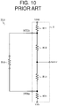
- FIG. 10 is an exemplary circuit diagram of a related-art temperature compensation circuit disclosed in US 2010/117637 .
- a related-art temperature compensation circuit BL1 includes resistors R11 to R14 that are connected in series in this order between a power supply terminal VDD and a ground terminal VSS, and a resistor R41.
- a first reference voltage VTH1 is output from a first output terminal NTH1 that is a node between the resistor R11 and the resistor R12
- a reference voltage VREF is output from a reference voltage terminal NREF that is a node between the resistor R12 and the resistor R13
- a second reference voltage VTH2 is output from a second output terminal NTH2 that is a node between the resistor R13 and the resistor R14.
- the resistor R41 is connected between the first output terminal NTH1 and the second output terminal NTH2.
- the resistors R11 to R14 have the same resistance value, the resistors R12 and R13 have the same resistance value, and the resistance values of the resistors R11 to R14 have the same temperature coefficient.
- the resistance value of the resistor R41 has a temperature coefficient that is different from the temperature coefficient of the resistance values of the resistors R11 to R14.
- the temperature coefficient of the resistance values of the resistors R11 to R14 is assumed to be larger than the temperature coefficient of the resistance value of the resistor R41. Then, the following expressions are established.
- RX is a resistance value between the first output terminal NTH1 and the second output terminal NTH2 and is expressed by the following expression.
- RX 2 ⁇ R 11 ⁇ R 41 2 ⁇ R 11 ⁇ R 41
- the temperature compensation amount can be adjusted.
- a temperature compensation circuit applicable to a wide range of sensor devices or semiconductor devices can be achieved with a small circuit scale.
- a temperature compensation circuit has the following configuration.
- the temperature compensation circuit includes: at least six resistors including a first resistor to a sixth resistor; a first output terminal connected to a node between the first resistor and the second resistor; a second output terminal connected to a node between the third resistor and the fourth resistor; a first voltage terminal formed at a node between the first resistor and the fourth resistor; and a second voltage terminal formed at a node between the second resistor and the third resistor, the fifth resistor being connected between a power supply terminal and the first voltage terminal, the sixth resistor being connected between a ground terminal and the second voltage terminal, in which a resistance value of at least one of the first resistor to the fourth resistor has a temperature coefficient that is different from a temperature coefficient of a resistance value of another of the first resistor to the fourth resistor, and in which the resistance value of the at least one of the first resistor to the fourth resistor is set so that a temperature compensation voltage that is output from the first output terminal and a temperature compensation voltage that is output from the second output terminal are equal
- a temperature compensation circuit that can adjust only the temperature coefficient and that can adjust the temperature compensation amount can be achieved with a relatively small circuit scale.
- a temperature compensation circuit according to the present invention can be widely used as a temperature compensation circuit in a semiconductor circuit.
- the temperature compensation circuit according to the present invention is described in the following with reference to the attached drawings.
- FIG. 1 is a circuit diagram of a temperature compensation circuit according to a first embodiment of the present invention.
- a temperature compensation circuit 1 according to the first embodiment includes resistors R1 to R6.
- a first output terminal Nr1 is connected to a node between the resistor R1 and the resistor R2.
- a second output terminal Nr2 is connected to a node between the resistor R3 and the resistor R4.
- a first voltage terminal Na is formed at a node between the resistor R1 and the resistor R4, and a second voltage terminal Nb is formed at a node between the resistor R2 and the resistor R3.
- the resistor R5 is connected between a power supply terminal VDD and the first voltage terminal Na, and the resistor R6 is connected between a ground terminal VSS and the second voltage terminal Nb.
- Vr1, Vr2, Va, and Vb Voltages at the first output terminal Nr1, at the second output terminal Nr2, at the first voltage terminal Na, and at the second voltage terminal Nb are represented by Vr1, Vr2, Va, and Vb, respectively.
- Vr1 and Vr2 are calculated by the following expressions.
- Vr 1 R 2 ⁇ Va + R 1 ⁇ Vb R 1 + R 2
- Vr 2 R 3 ⁇ Va + R 4 ⁇ Vb R 3 + R 4
- At least one resistor of the resistors R1 to R4 has a temperature coefficient that is different from a temperature coefficient of the resistance value of another of the resistors.
- FIG. 2 is a graph for showing temperature dependence of the resistance values of the resistors R1 to R4 used in the first embodiment.
- the resistance values of the resistors R1, R3, and R4 are equal to one another, the temperature coefficients of the respective resistance values are equal to one another, and the temperature coefficient of the resistance value of the resistor R2 is different from, in particular, smaller than, the temperature coefficient of the resistance values of the resistors R1, R3, and R4.
- the temperature coefficient of the resistance values of the resistors R1, R3, and R4 is referred to as a first temperature coefficient, while the temperature coefficient of the resistance value of the resistor R2 is referred to as a second temperature coefficient.
- the resistance value of the resistor R2 is smaller than the resistance value of the resistor R1, that is, ⁇ 1, and thus, the temperature compensation voltage ⁇ Vr is a negative value.
- the resistance value of the resistor R2 is larger than the resistance value of the resistor R1, that is, ⁇ >1, and thus, the temperature compensation voltage ⁇ Vr is a positive value. This is shown in FIG. 3 .
- FIG. 3 is a graph for showing temperature dependence of an output voltage according to the first embodiment.
- ⁇ Vr Vr1-Vr2 ⁇ 0, and thus, Vr1 ⁇ Vr2.
- ⁇ Vr Vr1-Vr2>0, and thus, Vr1>Vr2.
- the resistance values of the resistors R1 and R2 are adjusted so as to be equal to each other at the temperature T0, and thus, it is difficult to adjust the resistance values at a temperature other than the temperature T0.
- the resistor R5 and the resistor R6 are formed for the purpose of adjusting the temperature compensation voltage ⁇ Vr.
- Va VDD ⁇ I 5 ⁇ R 5
- Vb VSS ⁇ I 6 ⁇ R 6
- Va ⁇ Vb VDD ⁇ VSS ⁇ I 5 ⁇ R 5 + I 6 ⁇ R 6
- the temperature compensation circuit can solely and independently adjust the magnitude of the temperature compensation amount without skewing the distribution of temperature compensation amounts across a range of operating temperatures.
- the temperature coefficient of the resistance value of the resistor R1 may be different from that of the resistors R2 to R4, or the temperature coefficient of the resistance value of the resistor R3 may be different from that of the resistors R1, R2, and R4.
- the temperature coefficient of the resistance values of the resistors R1 and R3 may be equal to each other and the resistors R2 and R4 having a temperature coefficient of the resistance values that is different from that of the resistors R1 and R3 may be used.
- FIG. 4 is a circuit diagram of a temperature compensation circuit according to a second embodiment of the present invention.
- the second embodiment is different from the first embodiment illustrated in FIG. 1 in that a resistor R7 is added.
- the added resistor R7 is connected between the first voltage terminal Na and the second voltage terminal Nb.
- a resistor Ra' equivalent to the resistors R1 to R4 and the resistor R7 is expressed by the following expression.
- Ra ' R 7 R 7 + Ra ⁇ Ra
- (Va-Vb) is determined as in the following expressions.
- a term (1+Ra/R7) is added to the denominator. Specifically, adding the resistor R7 reduces the value of (Va-Vb). As the resistance value of the resistor R7 becomes smaller, (Va-Vb) becomes smaller, and the temperature compensation voltage ⁇ Vr expressed by Expression (3) or Expression (4) becomes smaller. In other words, through setting the resistance value of the resistor R7 to be an arbitrary value, (Va-Vb) can be arbitrarily adjusted, and thus, the temperature compensation voltage ⁇ Vr expressed by Expression (3) or Expression (4) can be arbitrarily adjusted.
- the temperature compensation circuit can solely and independently adjust the temperature compensation amount. Further, through setting the temperature coefficient of the resistance value of the resistor R7 so as to be different from the temperature coefficient of the resistance value of the equivalent resistor Ra, (Va-Vb) can also be temperature dependent, and thus, the temperature compensation voltage ⁇ Vr can be adjusted with more flexibility.
- FIG. 5 is a circuit diagram of a temperature compensation circuit according to a third embodiment of the present invention.
- the third embodiment is different from the first embodiment illustrated in FIG. 1 in that a resistor R8 is added.
- the added resistor R8 is connected between the first output terminal Nr1 and the second output terminal Nr2.
- a voltage Vr1' at the first output terminal Nr1, a voltage Vr2' at the second output terminal Nr2, and a temperature compensation voltage ⁇ Vr' in this embodiment are calculated as follows.
- currents flowing through the resistors R1 to R4 and R8 are represented by I1 to 14 and 18, respectively, the relationships of the respective currents are expressed by the following expressions.
- the temperature compensation circuit according to this embodiment can solely and independently adjust the temperature compensation amount.
- the temperature coefficient of the temperature compensation voltage ⁇ Vr' can be changed.
- the temperature compensation voltage ⁇ Vr can be adjusted with more flexibility.
- FIG. 6 is a graph for showing temperature dependence of sensitivity of a sensor element.
- temperature dependence of sensitivity of a Hall element which is an example of a magnetic sensor
- the sensitivity of a Hall element is generally in proportion to the mobility, and thus, as the temperature becomes higher, the sensitivity becomes lower.
- the sensitivity at the predetermined temperature T0 is represented by k0
- the sensitivity is lower than k0 at a temperature higher than the predetermined temperature T0
- the sensitivity is higher than k0 at a temperature lower than the predetermined temperature T0.
- FIG. 7 and FIG. 8 are illustrations of cases in which the temperature compensation circuit according to the present invention is applied to a sensor device.
- FIG. 7 is a circuit diagram of a case in which the temperature compensation circuit according to the present invention is applied to a magnetic sensor device.
- a signal from a Hall element 2 serving as a magneto-electric conversion element is input to a differential amplifier 4 via a switch circuit 3.
- the differential amplifier 4 amplifies the input signal, and the amplified signal is input to a comparator 5 via capacitors C1 and C2.
- the comparator 5 compares a difference between voltages respectively supplied to a terminal N1 and a terminal N2 and a difference between voltages respectively supplied to a terminal N3 and a terminal N4, based on signals responsive to a density of an applied magnetic flux, that is, output of the Hall element 2, and outputs whether the density of the applied magnetic flux is larger or smaller than a predetermined magnetic flux density.
- the switch circuit 3, switches S1 and S2, capacitors C1 to C4, and a reference voltage ref0 are used for the purpose of removing an error component of the Hall element 2, the differential amplifier 4, and the comparator 5 to obtain a highly accurate comparison result.
- the sensitivity of the Hall element 2 is temperature dependent, and thus, when the difference between the voltages supplied to the terminal N3 and the terminal N4, respectively, is constant when the temperature changes, the output of the comparator 5, that is, the output of the magnetic sensor device is an output that is not constant when the temperature changes, and is temperature dependent.
- the first output terminal Nr1 and the second output terminal Nr2 of the temperature compensation circuit 1 are connected to the terminal N3 and the terminal N4 via switches S3, S3x, S4, and S4x to supply the temperature compensation voltage ⁇ Vr or ⁇ Vr', thereby enabling obtainment of output of the magnetic sensor device without temperature dependence.
- FIG. 8 is a circuit diagram of another case in which the temperature compensation circuit according to the present invention is applied to a magnetic sensor device.
- the magnetic sensor device of FIG. 8 is different from the magnetic sensor device illustrated in FIG. 7 in that a reference voltage circuit 6 and switches S5, S5x, S6, and S6x are added.
- An output terminal Nr3 and an output terminal Nr4 of the reference voltage circuit 6 are connected to the terminal N3 and the terminal N4 via the switches S5, S5x, S6, and S6x to supply a reference voltage ⁇ Vref without temperature dependence. Therefore, the compensation amount at the predetermined temperature T0 can be supplied by the reference voltage circuit 6 and the temperature compensation amount can be supplied by the temperature compensation circuit 1.
- output of the magnetic sensor device without temperature dependence can be obtained, and at the same time, a threshold level for determining whether the density of the applied magnetic flux is larger or smaller than a predetermined magnetic flux density can be adjusted.
- FIG. 9 is a circuit diagram for illustrating an example of the reference voltage circuit 6 illustrated in FIG. 8 .
- the reference voltage circuit 6 includes resistors Rx1 to Rx3 that are connected in series between the power supply terminal VDD and the ground terminal VSS.
- the output terminal Nr3 is connected to a node between the resistors Rx1 and Rx2.
- the output terminal Nr4 is connected to a node between the resistors Rx2 and Rx3.
- the reference voltage ⁇ Vref is a voltage without temperature dependence. Further, through adjusting the ratio of the resistance values among the resistors Rx1 to Rx3, ⁇ Vref can be arbitrarily adjusted.
- FIG. 7 to FIG. 9 are illustrations of the cases in which the temperature compensation circuit according to the present invention is applied to a magnetic sensor device.
- specific cases are described herein, but the present invention is not necessarily limited to the configurations and the sensor element described herein, and is applicable to a wide range of semiconductor circuits.
Landscapes
- Physics & Mathematics (AREA)
- General Physics & Mathematics (AREA)
- Condensed Matter Physics & Semiconductors (AREA)
- Engineering & Computer Science (AREA)
- Health & Medical Sciences (AREA)
- Environmental & Geological Engineering (AREA)
- Toxicology (AREA)
- Electromagnetism (AREA)
- Radar, Positioning & Navigation (AREA)
- Automation & Control Theory (AREA)
- Measuring Magnetic Variables (AREA)
- Indication And Recording Devices For Special Purposes And Tariff Metering Devices (AREA)
- Measuring Temperature Or Quantity Of Heat (AREA)
- Semiconductor Integrated Circuits (AREA)
Applications Claiming Priority (1)
| Application Number | Priority Date | Filing Date | Title |
|---|---|---|---|
| JP2015112309A JP6511336B2 (ja) | 2015-06-02 | 2015-06-02 | 温度補償回路およびセンサ装置 |
Publications (2)
| Publication Number | Publication Date |
|---|---|
| EP3101440A1 EP3101440A1 (en) | 2016-12-07 |
| EP3101440B1 true EP3101440B1 (en) | 2018-08-01 |
Family
ID=56684426
Family Applications (1)
| Application Number | Title | Priority Date | Filing Date |
|---|---|---|---|
| EP16172517.1A Not-in-force EP3101440B1 (en) | 2015-06-02 | 2016-06-01 | Temperature compensation circuit and sensor device |
Country Status (6)
| Country | Link |
|---|---|
| US (1) | US10088532B2 (ko) |
| EP (1) | EP3101440B1 (ko) |
| JP (1) | JP6511336B2 (ko) |
| KR (1) | KR20160142240A (ko) |
| CN (1) | CN106227285B (ko) |
| TW (1) | TWI681197B (ko) |
Families Citing this family (6)
| Publication number | Priority date | Publication date | Assignee | Title |
|---|---|---|---|---|
| JP6994843B2 (ja) * | 2017-04-28 | 2022-01-14 | エイブリック株式会社 | 磁気センサ回路 |
| IT201700071189A1 (it) | 2017-06-26 | 2018-12-26 | St Microelectronics Srl | Circuito di compensazione in temperatura, dispositivo e procedimento corrispondenti |
| EP3467522B1 (en) * | 2017-10-06 | 2023-02-22 | STMicroelectronics S.r.l. | A temperature compensation circuit, corresponding device and method |
| EP3644080B1 (en) * | 2018-10-23 | 2022-08-03 | Melexis Bulgaria Ltd. | Sensor circuit with offset compensation |
| DE102020212114A1 (de) * | 2020-09-11 | 2022-03-17 | Fraunhofer-Gesellschaft zur Förderung der angewandten Forschung eingetragener Verein | Verfahren zum Bestimmen einer Empfindlichkeit eines Hallsensorelements und Hallsensor mit zumindest einem Hallsensorelement |
| CN113411074B (zh) * | 2021-07-13 | 2022-11-15 | 上海艾为电子技术股份有限公司 | 霍尔传感器开关及电子设备 |
Family Cites Families (26)
| Publication number | Priority date | Publication date | Assignee | Title |
|---|---|---|---|---|
| JPS5453877A (en) * | 1977-10-07 | 1979-04-27 | Hitachi Ltd | Temperature compensation circuit of semiconductor strain gauge |
| US4143549A (en) * | 1978-01-27 | 1979-03-13 | The United States Of America As Represented By The Secretary Of The Navy | Temperature measuring system |
| DE2940315C2 (de) * | 1978-10-10 | 1982-11-04 | Nippondenso Co., Ltd., Kariya, Aichi | Einrichtung zum Ermitteln des Drehwinkels eines Drehkörpers |
| JPS56140203A (en) * | 1980-04-02 | 1981-11-02 | Toyota Central Res & Dev Lab Inc | Bridge circuit |
| US4363243A (en) * | 1981-05-01 | 1982-12-14 | Eaton Corporation | Strain gage measurement circuit for high temperature applications using dual constant current supplies |
| JPS5896202U (ja) * | 1981-12-23 | 1983-06-30 | 株式会社石田衡器製作所 | 歪みゲ−ジの温度補償回路 |
| US4587499A (en) * | 1982-06-07 | 1986-05-06 | Toyo Communication Equipment Co., Ltd. | Temperature compensating circuit for oscillator |
| JPH0717029Y2 (ja) * | 1988-07-29 | 1995-04-19 | 横河電機株式会社 | 磁場検出回路 |
| US5121064A (en) * | 1990-08-31 | 1992-06-09 | Allied-Signal, Inc. | Method and apparatus for calibrating resistance bridge-type transducers |
| US5187985A (en) * | 1991-09-19 | 1993-02-23 | Honeywell Inc. | Amplified pressure transducer |
| US5253532A (en) * | 1992-03-09 | 1993-10-19 | Timex Corporation | Temperature compensated pressure transducer with digital output for low voltage power supply |
| US5402064A (en) * | 1992-09-02 | 1995-03-28 | Santa Barbara Research Center | Magnetoresistive sensor circuit with high output voltage swing and temperature compensation |
| US5953173A (en) * | 1996-09-17 | 1999-09-14 | International Business Machines Corporation | High CMRR and sensor-disk short-circuit protection device for dual element magnetoresistive heads |
| KR100314438B1 (ko) * | 1998-10-31 | 2002-04-24 | 구자홍 | 써모파일센서를이용한온도측정회로 |
| JP2002148131A (ja) * | 2000-11-10 | 2002-05-22 | Denso Corp | 物理量検出装置 |
| JP4236402B2 (ja) * | 2001-10-09 | 2009-03-11 | 富士通マイクロエレクトロニクス株式会社 | 半導体装置 |
| US20080088268A1 (en) * | 2004-09-24 | 2008-04-17 | Rohm Co., Ltd. | Fan Motor Drive Device and Cooler |
| JP2006121891A (ja) * | 2004-09-24 | 2006-05-11 | Rohm Co Ltd | ファンモータ駆動装置および冷却装置 |
| SG139588A1 (en) | 2006-07-28 | 2008-02-29 | St Microelectronics Asia | Addressable led architecure |
| JP5363074B2 (ja) | 2008-11-13 | 2013-12-11 | セイコーインスツル株式会社 | センサ回路 |
| JP5363075B2 (ja) * | 2008-11-13 | 2013-12-11 | セイコーインスツル株式会社 | センサ回路 |
| CN101594140A (zh) * | 2009-06-18 | 2009-12-02 | 浙江大学 | 一种薄膜体声波振荡器的温度漂移补偿方法和电路 |
| CN101706345A (zh) * | 2009-10-30 | 2010-05-12 | 江苏大学 | 一种用于微型压力传感器灵敏度热漂移的补偿方法 |
| JP6049488B2 (ja) * | 2013-02-14 | 2016-12-21 | エスアイアイ・セミコンダクタ株式会社 | センサ回路 |
| US9664752B2 (en) * | 2013-05-24 | 2017-05-30 | Allegro Microsystems, Llc | Magnetic field sensor for detecting a magnetic field in any direction above thresholds |
| CN104579172B (zh) * | 2014-11-28 | 2017-06-06 | 上海华虹宏力半导体制造有限公司 | 具有温度系数补偿的电阻电路 |
-
2015
- 2015-06-02 JP JP2015112309A patent/JP6511336B2/ja active Active
-
2016
- 2016-05-18 TW TW105115241A patent/TWI681197B/zh not_active IP Right Cessation
- 2016-05-26 US US15/165,445 patent/US10088532B2/en not_active Expired - Fee Related
- 2016-06-01 EP EP16172517.1A patent/EP3101440B1/en not_active Not-in-force
- 2016-06-01 KR KR1020160067941A patent/KR20160142240A/ko unknown
- 2016-06-02 CN CN201610384549.4A patent/CN106227285B/zh not_active Expired - Fee Related
Also Published As
| Publication number | Publication date |
|---|---|
| TWI681197B (zh) | 2020-01-01 |
| KR20160142240A (ko) | 2016-12-12 |
| US20160356862A1 (en) | 2016-12-08 |
| US10088532B2 (en) | 2018-10-02 |
| EP3101440A1 (en) | 2016-12-07 |
| JP2016223974A (ja) | 2016-12-28 |
| TW201643442A (zh) | 2016-12-16 |
| CN106227285B (zh) | 2019-08-16 |
| CN106227285A (zh) | 2016-12-14 |
| JP6511336B2 (ja) | 2019-05-15 |
Similar Documents
| Publication | Publication Date | Title |
|---|---|---|
| EP3101440B1 (en) | Temperature compensation circuit and sensor device | |
| KR101612359B1 (ko) | 교정식 온도 측정 시스템 | |
| KR101612360B1 (ko) | 온도 측정 시스템을 위한 입력 스테이지 | |
| EP2829889B1 (en) | Sensor device | |
| US9488529B2 (en) | Temperature measurement system | |
| TWI570388B (zh) | Sensing device | |
| EP3012971B1 (en) | Amplifier circuit and amplifier circuit ic chip | |
| JP2013149197A (ja) | 基準電圧発生回路 | |
| US9000824B2 (en) | Offset cancel circuit | |
| TWI668964B (zh) | 比較電路以及感測裝置 | |
| CN108732414B (zh) | 电流传感器及断路器 | |
| EP2338226B1 (en) | Low-voltage self-calibrated cmos peak detector | |
| JP6291224B2 (ja) | 磁気センサ | |
| JP4069158B1 (ja) | チャージアンプ、チャージアンプ装置、及び、バイアス電流補償方法 | |
| JP2005003596A (ja) | 抵抗測定装置、抵抗測定用集積回路及び抵抗測定方法 | |
| JP2019101043A (ja) | 物理的パラメーターを測定する電子デバイス | |
| US9768794B1 (en) | Analog-to-digital converter having a switched capacitor circuit | |
| US11946958B2 (en) | Current sensing circuit | |
| CN115248340A (zh) | 电流感测电路 | |
| JPH08159884A (ja) | 単電源を使用したロードセル式重量計の温度特性の補正方法 | |
| JP2014044111A (ja) | 二次電池装置及び充電状態計測方法 |
Legal Events
| Date | Code | Title | Description |
|---|---|---|---|
| PUAI | Public reference made under article 153(3) epc to a published international application that has entered the european phase |
Free format text: ORIGINAL CODE: 0009012 |
|
| STAA | Information on the status of an ep patent application or granted ep patent |
Free format text: STATUS: THE APPLICATION HAS BEEN PUBLISHED |
|
| AK | Designated contracting states |
Kind code of ref document: A1 Designated state(s): AL AT BE BG CH CY CZ DE DK EE ES FI FR GB GR HR HU IE IS IT LI LT LU LV MC MK MT NL NO PL PT RO RS SE SI SK SM TR |
|
| AX | Request for extension of the european patent |
Extension state: BA ME |
|
| STAA | Information on the status of an ep patent application or granted ep patent |
Free format text: STATUS: REQUEST FOR EXAMINATION WAS MADE |
|
| 17P | Request for examination filed |
Effective date: 20170607 |
|
| RBV | Designated contracting states (corrected) |
Designated state(s): AL AT BE BG CH CY CZ DE DK EE ES FI FR GB GR HR HU IE IS IT LI LT LU LV MC MK MT NL NO PL PT RO RS SE SI SK SM TR |
|
| RIC1 | Information provided on ipc code assigned before grant |
Ipc: G01R 33/00 20060101ALI20180322BHEP Ipc: G01R 33/07 20060101AFI20180322BHEP Ipc: H03K 17/14 20060101ALI20180322BHEP |
|
| GRAP | Despatch of communication of intention to grant a patent |
Free format text: ORIGINAL CODE: EPIDOSNIGR1 |
|
| RAP1 | Party data changed (applicant data changed or rights of an application transferred) |
Owner name: ABLIC INC. |
|
| STAA | Information on the status of an ep patent application or granted ep patent |
Free format text: STATUS: GRANT OF PATENT IS INTENDED |
|
| INTG | Intention to grant announced |
Effective date: 20180503 |
|
| GRAS | Grant fee paid |
Free format text: ORIGINAL CODE: EPIDOSNIGR3 |
|
| GRAA | (expected) grant |
Free format text: ORIGINAL CODE: 0009210 |
|
| STAA | Information on the status of an ep patent application or granted ep patent |
Free format text: STATUS: THE PATENT HAS BEEN GRANTED |
|
| AK | Designated contracting states |
Kind code of ref document: B1 Designated state(s): AL AT BE BG CH CY CZ DE DK EE ES FI FR GB GR HR HU IE IS IT LI LT LU LV MC MK MT NL NO PL PT RO RS SE SI SK SM TR |
|
| REG | Reference to a national code |
Ref country code: GB Ref legal event code: FG4D |
|
| REG | Reference to a national code |
Ref country code: CH Ref legal event code: EP Ref country code: AT Ref legal event code: REF Ref document number: 1024936 Country of ref document: AT Kind code of ref document: T Effective date: 20180815 |
|
| REG | Reference to a national code |
Ref country code: IE Ref legal event code: FG4D |
|
| REG | Reference to a national code |
Ref country code: DE Ref legal event code: R096 Ref document number: 602016004425 Country of ref document: DE |
|
| REG | Reference to a national code |
Ref country code: NL Ref legal event code: MP Effective date: 20180801 |
|
| REG | Reference to a national code |
Ref country code: LT Ref legal event code: MG4D |
|
| REG | Reference to a national code |
Ref country code: AT Ref legal event code: MK05 Ref document number: 1024936 Country of ref document: AT Kind code of ref document: T Effective date: 20180801 |
|
| PG25 | Lapsed in a contracting state [announced via postgrant information from national office to epo] |
Ref country code: SE Free format text: LAPSE BECAUSE OF FAILURE TO SUBMIT A TRANSLATION OF THE DESCRIPTION OR TO PAY THE FEE WITHIN THE PRESCRIBED TIME-LIMIT Effective date: 20180801 Ref country code: AT Free format text: LAPSE BECAUSE OF FAILURE TO SUBMIT A TRANSLATION OF THE DESCRIPTION OR TO PAY THE FEE WITHIN THE PRESCRIBED TIME-LIMIT Effective date: 20180801 Ref country code: RS Free format text: LAPSE BECAUSE OF FAILURE TO SUBMIT A TRANSLATION OF THE DESCRIPTION OR TO PAY THE FEE WITHIN THE PRESCRIBED TIME-LIMIT Effective date: 20180801 Ref country code: GR Free format text: LAPSE BECAUSE OF FAILURE TO SUBMIT A TRANSLATION OF THE DESCRIPTION OR TO PAY THE FEE WITHIN THE PRESCRIBED TIME-LIMIT Effective date: 20181102 Ref country code: NO Free format text: LAPSE BECAUSE OF FAILURE TO SUBMIT A TRANSLATION OF THE DESCRIPTION OR TO PAY THE FEE WITHIN THE PRESCRIBED TIME-LIMIT Effective date: 20181101 Ref country code: IS Free format text: LAPSE BECAUSE OF FAILURE TO SUBMIT A TRANSLATION OF THE DESCRIPTION OR TO PAY THE FEE WITHIN THE PRESCRIBED TIME-LIMIT Effective date: 20181201 Ref country code: PL Free format text: LAPSE BECAUSE OF FAILURE TO SUBMIT A TRANSLATION OF THE DESCRIPTION OR TO PAY THE FEE WITHIN THE PRESCRIBED TIME-LIMIT Effective date: 20180801 Ref country code: LT Free format text: LAPSE BECAUSE OF FAILURE TO SUBMIT A TRANSLATION OF THE DESCRIPTION OR TO PAY THE FEE WITHIN THE PRESCRIBED TIME-LIMIT Effective date: 20180801 Ref country code: BG Free format text: LAPSE BECAUSE OF FAILURE TO SUBMIT A TRANSLATION OF THE DESCRIPTION OR TO PAY THE FEE WITHIN THE PRESCRIBED TIME-LIMIT Effective date: 20181101 Ref country code: NL Free format text: LAPSE BECAUSE OF FAILURE TO SUBMIT A TRANSLATION OF THE DESCRIPTION OR TO PAY THE FEE WITHIN THE PRESCRIBED TIME-LIMIT Effective date: 20180801 Ref country code: FI Free format text: LAPSE BECAUSE OF FAILURE TO SUBMIT A TRANSLATION OF THE DESCRIPTION OR TO PAY THE FEE WITHIN THE PRESCRIBED TIME-LIMIT Effective date: 20180801 |
|
| PG25 | Lapsed in a contracting state [announced via postgrant information from national office to epo] |
Ref country code: LV Free format text: LAPSE BECAUSE OF FAILURE TO SUBMIT A TRANSLATION OF THE DESCRIPTION OR TO PAY THE FEE WITHIN THE PRESCRIBED TIME-LIMIT Effective date: 20180801 Ref country code: AL Free format text: LAPSE BECAUSE OF FAILURE TO SUBMIT A TRANSLATION OF THE DESCRIPTION OR TO PAY THE FEE WITHIN THE PRESCRIBED TIME-LIMIT Effective date: 20180801 Ref country code: HR Free format text: LAPSE BECAUSE OF FAILURE TO SUBMIT A TRANSLATION OF THE DESCRIPTION OR TO PAY THE FEE WITHIN THE PRESCRIBED TIME-LIMIT Effective date: 20180801 |
|
| PG25 | Lapsed in a contracting state [announced via postgrant information from national office to epo] |
Ref country code: IT Free format text: LAPSE BECAUSE OF FAILURE TO SUBMIT A TRANSLATION OF THE DESCRIPTION OR TO PAY THE FEE WITHIN THE PRESCRIBED TIME-LIMIT Effective date: 20180801 Ref country code: EE Free format text: LAPSE BECAUSE OF FAILURE TO SUBMIT A TRANSLATION OF THE DESCRIPTION OR TO PAY THE FEE WITHIN THE PRESCRIBED TIME-LIMIT Effective date: 20180801 Ref country code: ES Free format text: LAPSE BECAUSE OF FAILURE TO SUBMIT A TRANSLATION OF THE DESCRIPTION OR TO PAY THE FEE WITHIN THE PRESCRIBED TIME-LIMIT Effective date: 20180801 Ref country code: RO Free format text: LAPSE BECAUSE OF FAILURE TO SUBMIT A TRANSLATION OF THE DESCRIPTION OR TO PAY THE FEE WITHIN THE PRESCRIBED TIME-LIMIT Effective date: 20180801 Ref country code: CZ Free format text: LAPSE BECAUSE OF FAILURE TO SUBMIT A TRANSLATION OF THE DESCRIPTION OR TO PAY THE FEE WITHIN THE PRESCRIBED TIME-LIMIT Effective date: 20180801 |
|
| REG | Reference to a national code |
Ref country code: DE Ref legal event code: R097 Ref document number: 602016004425 Country of ref document: DE |
|
| PG25 | Lapsed in a contracting state [announced via postgrant information from national office to epo] |
Ref country code: DK Free format text: LAPSE BECAUSE OF FAILURE TO SUBMIT A TRANSLATION OF THE DESCRIPTION OR TO PAY THE FEE WITHIN THE PRESCRIBED TIME-LIMIT Effective date: 20180801 Ref country code: SM Free format text: LAPSE BECAUSE OF FAILURE TO SUBMIT A TRANSLATION OF THE DESCRIPTION OR TO PAY THE FEE WITHIN THE PRESCRIBED TIME-LIMIT Effective date: 20180801 Ref country code: SK Free format text: LAPSE BECAUSE OF FAILURE TO SUBMIT A TRANSLATION OF THE DESCRIPTION OR TO PAY THE FEE WITHIN THE PRESCRIBED TIME-LIMIT Effective date: 20180801 |
|
| PLBE | No opposition filed within time limit |
Free format text: ORIGINAL CODE: 0009261 |
|
| STAA | Information on the status of an ep patent application or granted ep patent |
Free format text: STATUS: NO OPPOSITION FILED WITHIN TIME LIMIT |
|
| 26N | No opposition filed |
Effective date: 20190503 |
|
| PG25 | Lapsed in a contracting state [announced via postgrant information from national office to epo] |
Ref country code: SI Free format text: LAPSE BECAUSE OF FAILURE TO SUBMIT A TRANSLATION OF THE DESCRIPTION OR TO PAY THE FEE WITHIN THE PRESCRIBED TIME-LIMIT Effective date: 20180801 |
|
| PG25 | Lapsed in a contracting state [announced via postgrant information from national office to epo] |
Ref country code: MC Free format text: LAPSE BECAUSE OF FAILURE TO SUBMIT A TRANSLATION OF THE DESCRIPTION OR TO PAY THE FEE WITHIN THE PRESCRIBED TIME-LIMIT Effective date: 20180801 |
|
| REG | Reference to a national code |
Ref country code: CH Ref legal event code: PL |
|
| REG | Reference to a national code |
Ref country code: BE Ref legal event code: MM Effective date: 20190630 |
|
| PG25 | Lapsed in a contracting state [announced via postgrant information from national office to epo] |
Ref country code: TR Free format text: LAPSE BECAUSE OF FAILURE TO SUBMIT A TRANSLATION OF THE DESCRIPTION OR TO PAY THE FEE WITHIN THE PRESCRIBED TIME-LIMIT Effective date: 20180801 |
|
| PG25 | Lapsed in a contracting state [announced via postgrant information from national office to epo] |
Ref country code: IE Free format text: LAPSE BECAUSE OF NON-PAYMENT OF DUE FEES Effective date: 20190601 |
|
| PG25 | Lapsed in a contracting state [announced via postgrant information from national office to epo] |
Ref country code: LI Free format text: LAPSE BECAUSE OF NON-PAYMENT OF DUE FEES Effective date: 20190630 Ref country code: BE Free format text: LAPSE BECAUSE OF NON-PAYMENT OF DUE FEES Effective date: 20190630 Ref country code: LU Free format text: LAPSE BECAUSE OF NON-PAYMENT OF DUE FEES Effective date: 20190601 Ref country code: CH Free format text: LAPSE BECAUSE OF NON-PAYMENT OF DUE FEES Effective date: 20190630 |
|
| PG25 | Lapsed in a contracting state [announced via postgrant information from national office to epo] |
Ref country code: PT Free format text: LAPSE BECAUSE OF FAILURE TO SUBMIT A TRANSLATION OF THE DESCRIPTION OR TO PAY THE FEE WITHIN THE PRESCRIBED TIME-LIMIT Effective date: 20181201 |
|
| PGFP | Annual fee paid to national office [announced via postgrant information from national office to epo] |
Ref country code: DE Payment date: 20200519 Year of fee payment: 5 Ref country code: FR Payment date: 20200512 Year of fee payment: 5 |
|
| GBPC | Gb: european patent ceased through non-payment of renewal fee |
Effective date: 20200601 |
|
| PG25 | Lapsed in a contracting state [announced via postgrant information from national office to epo] |
Ref country code: GB Free format text: LAPSE BECAUSE OF NON-PAYMENT OF DUE FEES Effective date: 20200601 |
|
| PG25 | Lapsed in a contracting state [announced via postgrant information from national office to epo] |
Ref country code: CY Free format text: LAPSE BECAUSE OF FAILURE TO SUBMIT A TRANSLATION OF THE DESCRIPTION OR TO PAY THE FEE WITHIN THE PRESCRIBED TIME-LIMIT Effective date: 20180801 |
|
| PG25 | Lapsed in a contracting state [announced via postgrant information from national office to epo] |
Ref country code: HU Free format text: LAPSE BECAUSE OF FAILURE TO SUBMIT A TRANSLATION OF THE DESCRIPTION OR TO PAY THE FEE WITHIN THE PRESCRIBED TIME-LIMIT; INVALID AB INITIO Effective date: 20160601 Ref country code: MT Free format text: LAPSE BECAUSE OF FAILURE TO SUBMIT A TRANSLATION OF THE DESCRIPTION OR TO PAY THE FEE WITHIN THE PRESCRIBED TIME-LIMIT Effective date: 20180801 |
|
| REG | Reference to a national code |
Ref country code: DE Ref legal event code: R119 Ref document number: 602016004425 Country of ref document: DE |
|
| PG25 | Lapsed in a contracting state [announced via postgrant information from national office to epo] |
Ref country code: DE Free format text: LAPSE BECAUSE OF NON-PAYMENT OF DUE FEES Effective date: 20220101 |
|
| PG25 | Lapsed in a contracting state [announced via postgrant information from national office to epo] |
Ref country code: FR Free format text: LAPSE BECAUSE OF NON-PAYMENT OF DUE FEES Effective date: 20210630 |
|
| PG25 | Lapsed in a contracting state [announced via postgrant information from national office to epo] |
Ref country code: MK Free format text: LAPSE BECAUSE OF FAILURE TO SUBMIT A TRANSLATION OF THE DESCRIPTION OR TO PAY THE FEE WITHIN THE PRESCRIBED TIME-LIMIT Effective date: 20180801 |