EP3100083B1 - Verfahren zum herstellen eines spiegelelements - Google Patents
Verfahren zum herstellen eines spiegelelements Download PDFInfo
- Publication number
- EP3100083B1 EP3100083B1 EP15705920.5A EP15705920A EP3100083B1 EP 3100083 B1 EP3100083 B1 EP 3100083B1 EP 15705920 A EP15705920 A EP 15705920A EP 3100083 B1 EP3100083 B1 EP 3100083B1
- Authority
- EP
- European Patent Office
- Prior art keywords
- layer stack
- mirror
- substrate
- curvature
- mirror element
- Prior art date
- Legal status (The legal status is an assumption and is not a legal conclusion. Google has not performed a legal analysis and makes no representation as to the accuracy of the status listed.)
- Active
Links
Images


Classifications
-
- G—PHYSICS
- G03—PHOTOGRAPHY; CINEMATOGRAPHY; ANALOGOUS TECHNIQUES USING WAVES OTHER THAN OPTICAL WAVES; ELECTROGRAPHY; HOLOGRAPHY
- G03F—PHOTOMECHANICAL PRODUCTION OF TEXTURED OR PATTERNED SURFACES, e.g. FOR PRINTING, FOR PROCESSING OF SEMICONDUCTOR DEVICES; MATERIALS THEREFOR; ORIGINALS THEREFOR; APPARATUS SPECIALLY ADAPTED THEREFOR
- G03F7/00—Photomechanical, e.g. photolithographic, production of textured or patterned surfaces, e.g. printing surfaces; Materials therefor, e.g. comprising photoresists; Apparatus specially adapted therefor
- G03F7/70—Microphotolithographic exposure; Apparatus therefor
- G03F7/70058—Mask illumination systems
- G03F7/702—Reflective illumination, i.e. reflective optical elements other than folding mirrors, e.g. extreme ultraviolet [EUV] illumination systems
-
- G—PHYSICS
- G02—OPTICS
- G02B—OPTICAL ELEMENTS, SYSTEMS OR APPARATUS
- G02B26/00—Optical devices or arrangements for the control of light using movable or deformable optical elements
- G02B26/08—Optical devices or arrangements for the control of light using movable or deformable optical elements for controlling the direction of light
- G02B26/0816—Optical devices or arrangements for the control of light using movable or deformable optical elements for controlling the direction of light by means of one or more reflecting elements
- G02B26/0833—Optical devices or arrangements for the control of light using movable or deformable optical elements for controlling the direction of light by means of one or more reflecting elements the reflecting element being a micromechanical device, e.g. a MEMS mirror, DMD
-
- G—PHYSICS
- G02—OPTICS
- G02B—OPTICAL ELEMENTS, SYSTEMS OR APPARATUS
- G02B5/00—Optical elements other than lenses
- G02B5/08—Mirrors
- G02B5/0816—Multilayer mirrors, i.e. having two or more reflecting layers
-
- G—PHYSICS
- G02—OPTICS
- G02B—OPTICAL ELEMENTS, SYSTEMS OR APPARATUS
- G02B5/00—Optical elements other than lenses
- G02B5/08—Mirrors
- G02B5/0891—Ultraviolet [UV] mirrors
-
- G—PHYSICS
- G02—OPTICS
- G02B—OPTICAL ELEMENTS, SYSTEMS OR APPARATUS
- G02B5/00—Optical elements other than lenses
- G02B5/08—Mirrors
- G02B5/09—Multifaceted or polygonal mirrors, e.g. polygonal scanning mirrors; Fresnel mirrors
-
- G—PHYSICS
- G02—OPTICS
- G02B—OPTICAL ELEMENTS, SYSTEMS OR APPARATUS
- G02B5/00—Optical elements other than lenses
- G02B5/08—Mirrors
- G02B5/10—Mirrors with curved faces
-
- G—PHYSICS
- G21—NUCLEAR PHYSICS; NUCLEAR ENGINEERING
- G21K—TECHNIQUES FOR HANDLING PARTICLES OR IONISING RADIATION NOT OTHERWISE PROVIDED FOR; IRRADIATION DEVICES; GAMMA RAY OR X-RAY MICROSCOPES
- G21K1/00—Arrangements for handling particles or ionising radiation, e.g. focusing or moderating
- G21K1/06—Arrangements for handling particles or ionising radiation, e.g. focusing or moderating using diffraction, refraction or reflection, e.g. monochromators
- G21K1/062—Devices having a multilayer structure
-
- G—PHYSICS
- G21—NUCLEAR PHYSICS; NUCLEAR ENGINEERING
- G21K—TECHNIQUES FOR HANDLING PARTICLES OR IONISING RADIATION NOT OTHERWISE PROVIDED FOR; IRRADIATION DEVICES; GAMMA RAY OR X-RAY MICROSCOPES
- G21K2201/00—Arrangements for handling radiation or particles
- G21K2201/06—Arrangements for handling radiation or particles using diffractive, refractive or reflecting elements
- G21K2201/064—Arrangements for handling radiation or particles using diffractive, refractive or reflecting elements having a curved surface
Definitions
- the invention relates to a method for producing a mirror element, in particular for a microlithographic projection exposure apparatus.
- Microlithography is used to fabricate microstructured devices such as integrated circuits or LCDs.
- the microlithography process is carried out in a so-called projection exposure apparatus which has an illumination device and a projection objective.
- mirrors are used as optical components for the imaging process, due to the lack of availability of suitable translucent refractive materials.
- facet mirrors in the form of field facet mirrors and pupil facet mirrors is in the illumination device of a microlithographic projection exposure apparatus designed for operation in the EUV as bundle-leading components eg from DE 10 2008 009 600 A1 known.
- Such facet mirrors are constructed from a multiplicity of individual mirrors or mirror facets, which in each case can be designed to be tiltable via rigid joints for the purpose of adjustment or else for the realization of specific illumination angle distributions.
- These mirror facets may in turn comprise a plurality of micromirrors.
- mirror arrangements eg WO 2005/026843 A2 known, which comprise a plurality of independently adjustable mirror elements.
- a problem encountered in practice is that in the manufacture of such a mirror assembly, e.g. a field facet mirror of a lighting device designed for operation in the EUV, mechanical stresses generated during the coating process (i.e., during the application of a layer stack including a reflective layer system to the mirror substrate), which can lead to a deformation of the substrate and a concomitant impairment of the optical imaging properties.
- mechanical stresses generated during the coating process i.e., during the application of a layer stack including a reflective layer system to the mirror substrate
- the respective refractive power of the mirror element as accurately as possible in the production of mirror elements (which, depending on the application, may be a refractive power of zero, corresponding to a planar mirror element, or a refractive power different from zero ).
- An approach known in this respect is, in the production of the mirror element, the substrate to be coated, inter alia, with the reflection layer system in its geometry before application of the layer stack, for example to form aspheres, fine corrections, etc., according to the desired To design the "final specification" of the mirror element and then perform the coating process (ie, the application of the layer stack including the reflective layer system), for example, using the aforementioned voltage compensation so that the shape of the substrate is not changed in the coating.
- the invention is based on the concept of eliminating the mechanical stress generated during production of a mirror element during the application of a layer stack including a reflective layer system to a substrate, not by an additional compensation layer (or a compensation layer system counteracting this mechanical tension), but rather to use the generated during the application of the layer stack including the reflective layer system on the substrate stress and thereby exerted by the layer stack on the substrate bending force targeted to produce a desired desired curvature of the mirror element - and thus a desired finite refractive power of the mirror element ,
- the substrate before the formation of the layer stack, the substrate has a curvature deviating from the desired desired curvature of the mirror element.
- the invention includes a deliberate departure from conventional approaches, in which the substrate is initially configured by suitable processing steps (eg by means of the formation of aspheres, fine corrections, etc.) according to the desired "final specification" of the mirror element and subsequently during application of Layer stack including the reflective layer system is ensured that the relevant, already deliberately given mirror substrate form is maintained by using stress-compensating layer (s).
- suitable processing steps eg by means of the formation of aspheres, fine corrections, etc.
- the present invention includes the principle, in the manufacture of a mirror element of a shape or geometry of the substrate prior to application of the reflective layer system-containing layer stack to go out, which does not yet correspond to the final desired for the finished mirror element curvature, then taking advantage of when applied the layer stack including the reflective layer system generated stress to deliberately deform the substrate.
- the ultimately resulting radius of curvature of the substrate and thus the refractive power of the finished mirror element is thus as a result of the original shape or geometry (including the thickness) of the substrate as well as the parameters set in the application of the layer stack including the reflective layer system (if necessary, as hereinafter explained with additional use of a post-treatment) achieved.
- an irreversible change in the curvature is caused by the bending force exerted by the layer stack, in particular by the aftertreatment for changing the layer tension of the layer stack.
- the aftertreatment for changing the layer tension of the layer stack may in particular comprise a thermal aftertreatment, eg by heating radiation, laser irradiation or tempering (wherein the aftertreatment takes place before the operation of the optical system or the projection exposure apparatus, ie even in the production of the relevant mirror element).
- the post-treatment may alternatively or additionally comprise ion irradiation or electron irradiation.
- the aftertreatment may also be locally limited to one or more subregions of the layer stack (which in their entirety are smaller than the entire extent or area of the layer stack), for example, by corner or edge regions of a mirror element in a different manner to treat as the remaining area of the relevant mirror element.
- the substrate has a locally varying rigidity, which is selected such that, after the formation of the layer stack, the desired curvature of the mirror element desired for the predetermined operating temperature is achieved.
- the rigidity is at least partially caused by a varying thickness profile of the substrate.
- suitable material-removing or material-adding methods can be used.
- the material addition may e.g. sputtering, electron beam deposition or any other material application method.
- the substrate is made of a first material, wherein the rigidity is at least partially effected by doping with impurities of a second material different from the first material.
- impurities of a second material different from the first material e.g. also an ion implantation possible.
- doped or implanted foreign atoms or ions may be, for example, oxygen, nitrogen, fluorine or hydrogen atoms or ions.
- a specific chemical change brought about in certain areas for example by oxidizing or nitriding the substrate material, for example a chemical conversion of silicon as substrate material to silicon dioxide (SiO 2 ) or silicon nitride (Si 3 N 4 ), which is specifically enhanced in the surface region laser treatment.
- a change in the morphology eg phase or crystal orientation
- the rigidity is at least partially caused by a structure or layer influencing the rigidity, which may be arranged in particular on the side of the substrate opposite to the layer stack.
- a structure may e.g. comprise additional lamellae on the side facing away from the reflection layer stack side of the substrate ("substrate back"), or also an additional, the stiffness influencing layer.
- such a structure or layer may also be arranged on the substrate front side or the side of the substrate facing the reflection layer stack.
- remaining gaps for example between lamellae with another material, or else with the same material with a different orientation, density, etc., can be replenished in order, for example, to achieve a homogeneous or smooth surface.
- the substrate is flat or convexly curved before forming the layer stack.
- the layer stack has an additional stress-inducing layer between the reflective layer system and the substrate.
- an additional stress-inducing layer may be used as a layer of a metallic material such as nickel, titanium, etc. or also e.g. as a (further) molybdenum-silicon stack with a high ⁇ value of e.g. more than 0.5 (wherein the ⁇ value as defined below, the ratio of absorber layer thickness to the total thickness of a period of the layer stack concerned indicates) and be designed specifically so that in the result the desired mechanical stress is generated in the layer system.
- the invention is not limited thereto, so that optionally the desired mechanical stress in the layer system can also be generated solely by the suitable design of the reflection layer system.
- the curvature exhibited by the substrate or mirror element is temperature-dependent, with one at a given Temperature concave curvature, for example, can go with increasing temperature in a convex curvature.
- the curvature or refractive power of the finished mirror element produced by means of the method according to the invention is generated taking into account this temperature dependence so that the desired (eg concave) curvature results just at the predetermined operating temperature.
- the desired desired curvature of the mirror element is a concave curvature.
- the o.g. Steps produced a plurality of mirror elements, wherein at least two of these mirror elements in the desired curvature differ from each other.
- the production of the mirror elements with mutually different desired curvature takes place in that a layer stack is applied to substrates of different thickness by setting the same bending force exerted by the respective layer stack.
- the production of the mirror elements with different nominal curvatures from each other takes place in that in each case a layer stack is applied to substrates of the same thickness while setting different bending forces exerted by the respective layer stack.
- the mirror element is a mirror element of a mirror arrangement composed of a plurality of mirror elements. These mirror elements can in particular be tilted independently of each other.
- the mirror arrangement is a facet mirror, in particular a field facet mirror or a pupil facet mirror.
- the mirror element is designed for an operating wavelength of less than 30 nm, in particular less than 15 nm.
- the invention is not limited thereto, so that in other applications the mirror element can also be designed for a wavelength in the VUV range, in particular a wavelength of less than 200 nm.
- the mirror element is a mirror element of a microlithographic projection exposure apparatus.
- the invention is not limited thereto, but also e.g. in measurement structures, which may be designed in particular for operation in the EUV, feasible.
- a readjustment of the curvature of the respective mirror element or the mirror elements can be carried out by adjusting the temperature of the respective mirror element.
- an adjustment of the curvature or refractive power of the individual mirror elements by a (in particular inhomogeneous) heating of the respective mirror element (or the mirror elements of the mirror assembly) take place the curvature of the mirror element in question varies depending on the operating temperature present in the corresponding position.
- a readjustment of the curvature or refractive power of the individual mirror elements can take place in that the temperature of the respective mirror elements or micromirrors is predetermined and set or regulated.
- a fine adjustment By means of the above-described inventive design of the reflection layer stack, taking advantage of the bending force, first a coarse adjustment of the curvature or refractive power and, via the last-mentioned temperature setting, a fine adjustment (“fine tuning”) are carried out.
- mirror elements produced may be (without the invention being restricted thereto), for example, mirror elements or micromirrors of a mirror arrangement in the form of a field facet mirror, wherein the individual mirror elements may have identical or even different curvatures or powers.
- each layer stack which has a reflection layer system (for example as a multilayer system of molybdenum and silicon layers) is applied to a substrate.
- the mirror substrate material may be, for example, silicon (Si) or titanium dioxide (TiO 2 ) -doped Quartz glass act, for example, the materials sold under the brand names ULE® (Corning Inc.) or Zerodur® (the company Schott AG) are used.
- the mirror substrate material may also include germanium (Ge), diamond, gallium arsenide (GaAs), gallium nitride (GaN), gallium antimonide (GaSb), gallium phosphide (GaP), Al 2 O 3 , indium phosphide (InP), indium arsenide (InAs), indium antimonide (InSb), calcium fluoride (CaF 2 ), zinc oxide (ZnO) or silicon carbide (SiC).
- germanium germanium
- diamond gallium arsenide
- GaN gallium nitride
- GaSb gallium antimonide
- GaP gallium phosphide
- Al 2 O 3 Al 2 O 3
- InP indium arsenide
- InAs indium antimonide
- SiC silicon carbide
- further functional layers such as, for example, a cover layer ("cap layer"), a substrate protective layer, etc., may be provided in a
- a bending force of the layer stack which differs from zero is exerted on the substrate by suitably setting the coating parameters and / or the parameters of a post-treatment and the mechanical stress generated thereby in each case during the formation of the layer stack comprising the reflection layer system.
- the setting of the mechanical stress during formation of the respective layer stack takes place according to the invention in a manner known per se by setting materials and thickness ratios (eg the ratio of absorber layer thickness to total thickness of a period, this thickness ratio also being designated as)) in the desired manner, in particular in the reflective layer system become.
- the procedure when setting a mechanical tension is the expert from eg DE 10 2008 042 212 A1 known.
- the adjustment of the mechanical stress when applying the respective layer stack can also be effected by oxygen doping or addition of oxygen during coating, as is known to the person skilled in the art DE 10 2011 003 357 A1 is known.
- the said initial curvature of the substrate in the pre-coating state may be either zero (ie, the substrate is flat prior to coating), or the original curvature may correspond to a finite curvature (eg, a convex curvature) that does not yet correspond to the desired desired curvature of the finished mirror element ,
- Fig. 1-5 differ in the way in which the different mirror elements (eg a mirror arrangement such as a field facet mirror) depending on the initial shape or original curvature of the substrate in the state before the coating, setting the coating parameters with respect to the generated mechanical stress and optionally ( eg thermal) aftertreatment can be made with identical or different curvature.
- the different mirror elements eg a mirror arrangement such as a field facet mirror
- setting the coating parameters with respect to the generated mechanical stress and optionally (eg thermal) aftertreatment can be made with identical or different curvature.
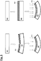
- a plurality of mirror elements of the same curvature or refractive power can be produced by planar (mirror) substrates 101, 102,... each with a layer stack 111, 112,... including a reflective layer system while setting identical coating parameters be coated, wherein during this coating, the generated mechanical stress and the resulting bending force to the respective substrate 101, 102, ... are selected such that adjusts the desired (for each mirror elements in each case identical) curvature in each finished mirror element.
- the respective substrates 103, 104,... may also have a finite curvature in the initial state (before the coating) which does not yet correspond to the curvature ultimately desired, this substrate curvature then being determined by the mechanical stress or bending force generated when the layer stack is applied is changed.
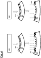
- Fig. 2 and 3 serve to explain possible further embodiments for the production of a micromirror arrangement, for example in the form of a field facet mirror, in which individual mirror elements are intended to have mutually different curvatures or different refractive powers.
- Fig. 1 analogous or substantially functionally identical components in Fig. 2 with reference numbers increased by "100” and in Fig. 3 with reference numbers increased by "200".
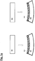
- planar substrates 201, 202,... which, however, have different thicknesses from one another, are each coated with a layer stack while setting the same mechanical stress or bending force. As in the lower part of Fig. 2 is indicated, this leads due to the different substrate thicknesses to produce different curvatures of the finished mirror elements (wherein Fig. 2 the generated curvature is greater with a smaller substrate thickness).
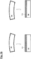
- Fig. 3 the generation of different curvatures in the finally produced mirror elements is to some extent reversed Fig. 2 in that (in the example again planar) substrates 301, 302, ... of the same thickness are coated with layer stacks 311, 312,... with generation of different mechanical stresses or bending forces.
- substrates 301, 302, ... of the same thickness are coated with layer stacks 311, 312,... with generation of different mechanical stresses or bending forces.
- a higher layer stress (right part of Fig. 3 ) result in a greater curvature in the finally manufactured mirror element.
- a higher layer tension can lead to a comparatively smaller curvature even in the final state.
- mirror elements with mutually different curvature can also be produced in that individual substrates with the same thickness and geometry of a coating in the initial state (ie before the coating) (ie application of the layer stack including of the reflection layer system) with identical parameters (to produce the same mechanical stress), but then a (in particular thermal) aftertreatment is carried out, by means of which the mechanical stress generated in each case in the layer stacks of the individual mirror elements is subsequently changed.
- a post-treatment may include, for example, annealing in an oven (setting a defined atmosphere), thermal post-treatment using a radiant heater, or post-treatment under laser irradiation, ion irradiation, or electron beam irradiation (as well as combinations of these methods).
- suitable cooling can be carried out from the back of the mirror.
- the laser irradiation if appropriate using a mask which exposes only the areas to be aftertreated, such as, for example, corners of the mirror element
- corner or edge regions of a mirror element can be aftertreated or deformed in a manner different from the remaining region of the relevant mirror element.
- the aftertreatment described above can be carried out either individually for all mirror elements produced in an identical manner, for individual mirror elements (or even larger units of a plurality of mirror elements in the form of mirror arrays) individually or else as locally described above individual mirror elements.
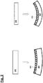
- Fig. 4 shows to illustrate this principle, as an initially uniform or identical coating of substrates 401, 402, ..., each with a layer stack 411, 412, ... initially to an identical curvature (middle part of Fig. 4 ), but then leads by way of different post-treatments to different curvature or refractive power of each manufactured mirror elements.
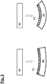
- the aftertreatment described above can also be used to a first generated after formation of the layer stack including the reflective layer system on the substrate or even before the coating present undesirable (eg, inhomogeneous or for a plurality of substrates 501, 502, ... varying) curvature, such as may result from process fluctuations in the individual coating processes, to "homogenize” with the result that the finally manufactured mirror elements have the same curvature or refractive power.
- undesirable curvature such as may result from process fluctuations in the individual coating processes
- the mirror element in question may be a mirror element of a micromirror arrangement, for example a field facet mirror.
- This approach is based on the consideration that a specific influencing of the stiffness of the substrate determines its "reaction" to the bending force exerted by the layer stack including the reflection layer system and thus is also suitable for ultimately bringing about a desired surface geometry or desired curvature of the mirror element contribute to this.
- a substrate 801 has been thinned in a plurality of regions 801a (only by way of example as spokes), for example by means of etching, so that it has a comparatively greater thickness in the remaining regions 801b.
- Fig. 9a and 9b show in rear view ( Fig. 9a ) or cross section ( Fig. 9b ) merely by way of example a further embodiment a substrate 901 with continuous radial thickness reduction.
- a continuous thickness variation according to Fig. 9b also with the design of Fig. 8a (ie, the corresponding geometry of the respective areas in rear view), or it may be the thickness variation according to Fig. 8b with the embodiment according to Fig. 9a (ie the corresponding geometry of the respective areas in rear view), etc.
- FIG. 10a and 10b also show by way of example only further embodiments, wherein in Fig. 10a a substrate 951 has been thinned in circular regions 951a of different sizes (again to produce regions 951a and 951b of different thickness, respectively), and according to FIG Fig. 10b a substrate 961 with radially arranged thin webs (as areas 961b of greater thickness, between which thus are also relatively thinner areas 961a) was provided.
- the invention is not limited to a material-removing or material-adding processing of the substrate with regard to the rigidity influencing of the substrate.
- the stiffness influence of the substrate at least partially by doping with impurities or ion implantation eg of oxygen, nitrogen, fluorine or hydrogen atoms or ions
- impurities or ion implantation eg of oxygen, nitrogen, fluorine or hydrogen atoms or ions
- laser treatment or by a structure affecting the rigidity
- a structure affecting the rigidity can be effected, which in particular on the side opposite to the layer stack side of the substrate ("substrate back") can be arranged.
- An arrangement on the side of the substrate facing the layer stack (“substrate front side) is likewise possible, care being taken that the desired optical properties are not impaired.
- the respective intermediate spaces in a structure for example between lamellae, can be refilled with another material or else with the same material with different orientation, density, etc., in order, for example, to achieve a homogeneous or smooth surface.
- an additional layer influencing the stiffness may also be provided on the side of the substrate facing away from the reflection layer stack.
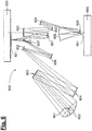
- Fig. 6 shows a schematic representation of an exemplary designed for operation in the EUV projection exposure equipment in which the present invention is feasible.
- a lighting device in an EUV-designed projection exposure apparatus 600 has a field facet mirror 603 and a pupil facet mirror 604.
- the light of a light source unit comprising a plasma light source 601 and a collector mirror 602 is directed.
- a first telescope mirror 605 and a second telescope mirror 606 are arranged in the light path after the pupil facet mirror 604.
- a deflecting mirror 607 is arranged downstream of the light path, which deflects the radiation impinging on it onto an object field in the object plane of a projection objective comprising six mirrors 651-656.
- a reflective structure-carrying mask 621 is arranged on a mask table 620, which is imaged by means of the projection lens into an image plane in which a photosensitive layer (photoresist) -coated substrate 661 is located on a wafer table 660.
- the method according to the invention is particularly advantageous for the production of the field facet mirror 603 Fig. 6 applicable, in particular, when the individual field facets of the field facet mirror 603 are in turn composed of individual mirror elements or micromirrors.
- Such a "sub-faceting" of the field facet mirror is known to those skilled in the art US 2011/0001947 A1 known and can as in Fig. 7 Shown schematically on the basis of a single field facet 700, for example, such that a plurality of respective planar mirror elements 701, 702, 703,... pass through in such a way corresponding adjustment of the normal vectors can be strung together so that as a result the typically spherical surface of the (macroscopic) mirror facet is reproduced.
- the optical effect of the pupil facets of the pupil facet mirror 604 can be made Fig. 6 by a "false" refractive power of the individual mirror elements 701, 702, 703,... or of the field facets 700 of the field facet mirror 603 Fig. 6 be affected.
- the invention is not limited to the application to the facet mirror, so that in principle also other mirrors (even those which are not composed of a plurality of mirror elements) can be configured in the manner according to the invention.
Landscapes
- Physics & Mathematics (AREA)
- General Physics & Mathematics (AREA)
- Optics & Photonics (AREA)
- Spectroscopy & Molecular Physics (AREA)
- Engineering & Computer Science (AREA)
- General Engineering & Computer Science (AREA)
- High Energy & Nuclear Physics (AREA)
- Optical Elements Other Than Lenses (AREA)
- Exposure And Positioning Against Photoresist Photosensitive Materials (AREA)
Applications Claiming Priority (2)
| Application Number | Priority Date | Filing Date | Title |
|---|---|---|---|
| DE102014201622.3A DE102014201622A1 (de) | 2014-01-30 | 2014-01-30 | Verfahren zum Herstellen eines Spiegelelements |
| PCT/EP2015/051791 WO2015114043A1 (de) | 2014-01-30 | 2015-01-29 | Verfahren zum herstellen eines spiegelelements |
Publications (2)
| Publication Number | Publication Date |
|---|---|
| EP3100083A1 EP3100083A1 (de) | 2016-12-07 |
| EP3100083B1 true EP3100083B1 (de) | 2019-08-14 |
Family
ID=52574101
Family Applications (1)
| Application Number | Title | Priority Date | Filing Date |
|---|---|---|---|
| EP15705920.5A Active EP3100083B1 (de) | 2014-01-30 | 2015-01-29 | Verfahren zum herstellen eines spiegelelements |
Country Status (6)
| Country | Link |
|---|---|
| US (1) | US10423073B2 (enExample) |
| EP (1) | EP3100083B1 (enExample) |
| JP (1) | JP6550066B2 (enExample) |
| CN (1) | CN105917255B (enExample) |
| DE (1) | DE102014201622A1 (enExample) |
| WO (1) | WO2015114043A1 (enExample) |
Families Citing this family (11)
| Publication number | Priority date | Publication date | Assignee | Title |
|---|---|---|---|---|
| DE102015225510A1 (de) * | 2015-12-16 | 2017-01-12 | Carl Zeiss Smt Gmbh | Spiegelelement, insbesondere für eine mikrolithographische Projektionsbelichtungsanlage |
| FR3065536B1 (fr) * | 2017-04-20 | 2019-07-12 | Alpao | Miroir deformable a courbure variable et procede de fabrication d'un miroir associe |
| CN107143756B (zh) * | 2017-06-14 | 2020-05-08 | 上海安茗科技中心(有限合伙) | 灯具 |
| DE102019202222B4 (de) * | 2019-02-19 | 2023-08-10 | Fraunhofer-Gesellschaft zur Förderung der angewandten Forschung e.V. | Ablenkspiegel aus Diamant sowie Verfahren zur Herstellung |
| EP3703114A1 (en) * | 2019-02-26 | 2020-09-02 | ASML Netherlands B.V. | Reflector manufacturing method and associated reflector |
| DE102023200603A1 (de) | 2023-01-26 | 2024-08-01 | Carl Zeiss Smt Gmbh | Verfahren zum Herstellen einer Spiegelanordnung, sowie Beschichtungsanlage |
| DE102023205340A1 (de) | 2023-06-07 | 2024-12-12 | Carl Zeiss Smt Gmbh | Verfahren zum Herstellen eines optischen Elements, sowie optisches Element und Beschichtungsanlage |
| DE102023206689A1 (de) | 2023-07-13 | 2025-01-16 | Carl Zeiss Smt Gmbh | Aktuierbare Spiegel-Baugruppe |
| DE102023210486A1 (de) * | 2023-10-24 | 2025-04-24 | Carl Zeiss Smt Gmbh | Optisches Element und EUV-Lithographiesystem |
| JP7519150B1 (ja) * | 2024-04-11 | 2024-07-19 | 合同会社北海道環境・エネルギー研究所 | 柱面体作製方法及びその作製方法を用いて作製された柱面体 |
| DE102024205025A1 (de) * | 2024-05-29 | 2025-12-04 | Carl Zeiss Smt Gmbh | Mikro-elektro-mechanisch bewegbares Element und System |
Family Cites Families (39)
| Publication number | Priority date | Publication date | Assignee | Title |
|---|---|---|---|---|
| JPS58217901A (ja) * | 1982-06-14 | 1983-12-19 | Nippon Kogaku Kk <Nikon> | 透過型光学部材 |
| JPH06186418A (ja) * | 1992-06-30 | 1994-07-08 | Victor Co Of Japan Ltd | ダイクロイックミラーの製造方法 |
| JPH09197124A (ja) * | 1996-01-23 | 1997-07-31 | Nippon Electric Glass Co Ltd | ダイクロイックミラー |
| US6011646A (en) * | 1998-02-20 | 2000-01-04 | The Regents Of The Unviersity Of California | Method to adjust multilayer film stress induced deformation of optics |
| US6110607A (en) * | 1998-02-20 | 2000-08-29 | The Regents Of The University Of California | High reflectance-low stress Mo-Si multilayer reflective coatings |
| KR100647968B1 (ko) | 1999-07-22 | 2006-11-17 | 코닝 인코포레이티드 | 극 자외선 소프트 x-선 투사 리소그라피 방법 및 마스크디바이스 |
| US6737201B2 (en) | 2000-11-22 | 2004-05-18 | Hoya Corporation | Substrate with multilayer film, reflection type mask blank for exposure, reflection type mask for exposure and production method thereof as well as production method of semiconductor device |
| JP3939132B2 (ja) * | 2000-11-22 | 2007-07-04 | Hoya株式会社 | 多層膜付き基板、露光用反射型マスクブランク、露光用反射型マスクおよびその製造方法、並びに半導体の製造方法 |
| JP4320970B2 (ja) * | 2001-04-11 | 2009-08-26 | 株式会社ニコン | 多層膜反射鏡の製造方法 |
| DE10314212B4 (de) | 2002-03-29 | 2010-06-02 | Hoya Corp. | Verfahren zur Herstellung eines Maskenrohlings, Verfahren zur Herstellung einer Transfermaske |
| US7056627B2 (en) | 2002-08-23 | 2006-06-06 | Hoya Corporation | Method of manufacturing a reflection type mask blank and method of manufacturing a reflection type mask |
| US7314688B2 (en) * | 2002-09-11 | 2008-01-01 | Hoya Corporation | Method of producing a reflection mask blank, method of producing a reflection mask, and method of producing a semiconductor device |
| JP3806711B2 (ja) * | 2002-09-11 | 2006-08-09 | Hoya株式会社 | 反射型マスクブランク及び反射型マスクの製造方法、並びに半導体装置の製造方法 |
| US6778315B2 (en) | 2002-09-25 | 2004-08-17 | Rosemount Aerospace Inc. | Micro mirror structure with flat reflective coating |
| US20050026332A1 (en) * | 2003-07-29 | 2005-02-03 | Fratti Roger A. | Techniques for curvature control in power transistor devices |
| JP4717813B2 (ja) | 2003-09-12 | 2011-07-06 | カール・ツァイス・エスエムティー・ゲーエムベーハー | マイクロリソグラフィ投影露光設備のための照明系 |
| WO2006092919A1 (ja) * | 2005-02-28 | 2006-09-08 | Nikon Corporation | 光学素子及び光学素子の製造方法 |
| US20080166534A1 (en) | 2005-02-28 | 2008-07-10 | Nikon Corporation | Optical Element and Method for Manufacturing Optical Element |
| DE102005044716A1 (de) | 2005-09-19 | 2007-04-05 | Carl Zeiss Smt Ag | Aktives optisches Element |
| JP2007108194A (ja) * | 2005-10-11 | 2007-04-26 | Canon Inc | 多層膜ミラーの製造方法、光学系の製造方法、露光装置、及びデバイス製造方法 |
| EP1945829A1 (en) * | 2005-11-10 | 2008-07-23 | Asahi Glass Company, Limited | Method for depositing reflective multilayer film of reflective mask blank for euv lithography and method for producing reflective mask blank for euv lithography |
| JP2008109060A (ja) * | 2005-11-10 | 2008-05-08 | Asahi Glass Co Ltd | Euvリソグラフィ用反射型マスクブランクの多層反射膜を成膜する方法、ならびにeuvリソグラフィ用反射型マスクブランクの製造方法 |
| JP2007193131A (ja) * | 2006-01-19 | 2007-08-02 | Seiko Epson Corp | 光学部品の製造方法 |
| JP2007329368A (ja) | 2006-06-09 | 2007-12-20 | Canon Inc | 多層膜ミラー、評価方法、露光装置及びデバイス製造方法 |
| JP2008101916A (ja) * | 2006-10-17 | 2008-05-01 | Canon Inc | 多層膜光学素子 |
| US20080153010A1 (en) * | 2006-11-09 | 2008-06-26 | Asahi Glass Company., Ltd. | Method for depositing reflective multilayer film of reflective mask blank for euv lithography and method for producing reflective mask blank for euv lithography |
| JP4269189B2 (ja) * | 2007-03-16 | 2009-05-27 | フジノン株式会社 | 光学素子、光学膜平面化方法及び光学素子の製造方法 |
| US8194322B2 (en) * | 2007-04-23 | 2012-06-05 | Nikon Corporation | Multilayer-film reflective mirror, exposure apparatus, device manufacturing method, and manufacturing method of multilayer-film reflective mirror |
| US20100246036A1 (en) * | 2007-07-27 | 2010-09-30 | Lagana Paolo | Preliminary Controlled Pre-Deformation Treatment for the Production of Mirrors |
| DE102008009600A1 (de) | 2008-02-15 | 2009-08-20 | Carl Zeiss Smt Ag | Facettenspiegel zum Einsatz in einer Projektionsbelichtungsanlage für die Mikro-Lithographie |
| CN101946190B (zh) | 2008-02-15 | 2013-06-19 | 卡尔蔡司Smt有限责任公司 | 微光刻的投射曝光设备使用的分面镜 |
| DE102008042212A1 (de) | 2008-09-19 | 2010-04-01 | Carl Zeiss Smt Ag | Reflektives optisches Element und Verfahren zu seiner Herstellung |
| JP5525550B2 (ja) * | 2009-03-06 | 2014-06-18 | カール・ツァイス・エスエムティー・ゲーエムベーハー | マイクロリソグラフィ用の照明光学系及び光学系 |
| DE102009033511A1 (de) | 2009-07-15 | 2011-01-20 | Carl Zeiss Smt Ag | Mikrospiegelanordnung mit Anti-Reflexbeschichtung sowie Verfahren zu deren Herstellung |
| CN102565901B (zh) | 2010-12-17 | 2014-06-04 | 北京兆阳光热技术有限公司 | 一种曲面反射镜及其制造方法 |
| DE102011003357A1 (de) | 2011-01-31 | 2012-08-02 | Carl Zeiss Smt Gmbh | Spiegel für den EUV-Wellenlängenbereich, Herstellungsverfahren für einen solchen Spiegel, Projektionsobjektiv für die Mikrolithographie mit einem solchen Spiegel und Projektionsbelichtungsanlage für die Mikrolithographie mit einem solchen Projektionsobjektiv |
| CN102759765B (zh) * | 2011-04-28 | 2014-11-05 | 北京兆阳光热技术有限公司 | 一种曲面反射镜及其制造方法 |
| DE102011084117A1 (de) * | 2011-10-07 | 2013-04-11 | Carl Zeiss Smt Gmbh | Reflektives optisches Element für den EUV-Wellenlängenbereich, Verfahren zur Erzeugung und zur Korrektur eines solchen Elements, Projektionsobjektiv für die Mikrolithographie mit einem solchen Element und Projektionsbelichtungsanlage für die Mikrolithographie mit einem solchen Projektionsobjektiv |
| WO2013077430A1 (ja) * | 2011-11-25 | 2013-05-30 | 旭硝子株式会社 | Euvリソグラフィ用反射型マスクブランクおよびその製造方法 |
-
2014
- 2014-01-30 DE DE102014201622.3A patent/DE102014201622A1/de not_active Ceased
-
2015
- 2015-01-29 WO PCT/EP2015/051791 patent/WO2015114043A1/de not_active Ceased
- 2015-01-29 CN CN201580004334.9A patent/CN105917255B/zh active Active
- 2015-01-29 EP EP15705920.5A patent/EP3100083B1/de active Active
- 2015-01-29 JP JP2016549378A patent/JP6550066B2/ja active Active
-
2016
- 2016-08-01 US US15/225,328 patent/US10423073B2/en active Active
Non-Patent Citations (1)
| Title |
|---|
| None * |
Also Published As
| Publication number | Publication date |
|---|---|
| CN105917255A (zh) | 2016-08-31 |
| CN105917255B (zh) | 2019-10-25 |
| DE102014201622A1 (de) | 2015-08-20 |
| JP2017506363A (ja) | 2017-03-02 |
| US10423073B2 (en) | 2019-09-24 |
| JP6550066B2 (ja) | 2019-07-24 |
| EP3100083A1 (de) | 2016-12-07 |
| WO2015114043A1 (de) | 2015-08-06 |
| US20160342093A1 (en) | 2016-11-24 |
Similar Documents
| Publication | Publication Date | Title |
|---|---|---|
| EP3100083B1 (de) | Verfahren zum herstellen eines spiegelelements | |
| EP3286595B1 (de) | Wellenfrontkorrekturelement zur verwendung in einem optischen system | |
| WO2015043832A1 (de) | Spiegel, insbesondere für eine mikrolithographische projektionsbelichtungsanlage | |
| EP3791219B9 (de) | Spiegel, insbesondere für eine mikrolithographische projektionsbelichtungsanlage | |
| DE102014219755A1 (de) | Reflektives optisches Element | |
| DE102015200328A1 (de) | Verfahren zum Herstellen eines optischen Elements für ein optisches System, insbesondere für einemikrolithographische Projektionsbelichtungsanlage | |
| DE102016210794A1 (de) | Optische Anordnung, EUV-Lithographieanlage und Verfahren zum Betrieb der optischen Anordnung | |
| EP3030936B1 (de) | Spiegel für eine mikrolithographische projektionsbelichtungsanlage | |
| EP4212962A1 (de) | Verfahren und vorrichtung zum bestimmen des erwärmungszustandes eines optischen elements in einem optischen system für die mikrolithographie | |
| WO2023242060A1 (de) | Verfahren zum heizen eines optischen elements sowie optisches system | |
| DE102015225510A1 (de) | Spiegelelement, insbesondere für eine mikrolithographische Projektionsbelichtungsanlage | |
| DE102015204478A1 (de) | Verfahren zum Glätten einer Oberfläche und optisches Element | |
| DE102014219648A1 (de) | Verfahren zum Herstellen eines Spiegelelements | |
| DE102011006003A1 (de) | Beleuchtungsoptik zum Einsatz in einer Projektionsbelichtungsanlage für die Mikrolithografie | |
| WO2024033083A1 (de) | Verfahren zur stabilisierung einer klebstoffverbindung einer optischen baugruppe, optische baugruppe und projektionsbelichtungsanlage für die halbleiterlithographie | |
| WO2024251468A1 (de) | Verfahren zum herstellen eines optischen elements, sowie optisches element und beschichtungsanlage | |
| WO2024061579A1 (de) | Anordnung zum tempern mindestens eines teilbereichs eines optischen elementes | |
| WO2023237282A1 (de) | Verfahren zum betreiben einer projektionsbelichtungsanlage und projektionsbelichtungsanlage | |
| DE102021208664A1 (de) | Spiegel für eine Projektionsbelichtungsanlage der Mikrolithographie | |
| DE102011084650A1 (de) | Diffraktive optische Elemente für EUV-Strahlung | |
| DE102021203475A1 (de) | Verfahren zur Herstellung eines Spiegels einer Projektionsbelichtungsanlage für die Mikrolithographie | |
| DE102023206061B4 (de) | Verfahren zum Korrigieren eines Oberflächenfehlers an einem Spiegel | |
| DE102017213398A1 (de) | Verfahren zum Bearbeiten eines Werkstücks bei der Herstellung eines optischen Elements | |
| DE102022116700A1 (de) | Optische Baugruppe, Projektionsbelichtungsanlage für die Halbleiterlithographie und Verfahren | |
| WO2022180004A1 (de) | Optische baugruppe, verfahren zur deformation eines optischen elements und projektionsbelichtungsanlage |
Legal Events
| Date | Code | Title | Description |
|---|---|---|---|
| PUAI | Public reference made under article 153(3) epc to a published international application that has entered the european phase |
Free format text: ORIGINAL CODE: 0009012 |
|
| STAA | Information on the status of an ep patent application or granted ep patent |
Free format text: STATUS: REQUEST FOR EXAMINATION WAS MADE |
|
| 17P | Request for examination filed |
Effective date: 20160608 |
|
| AK | Designated contracting states |
Kind code of ref document: A1 Designated state(s): AL AT BE BG CH CY CZ DE DK EE ES FI FR GB GR HR HU IE IS IT LI LT LU LV MC MK MT NL NO PL PT RO RS SE SI SK SM TR |
|
| AX | Request for extension of the european patent |
Extension state: BA ME |
|
| DAX | Request for extension of the european patent (deleted) | ||
| STAA | Information on the status of an ep patent application or granted ep patent |
Free format text: STATUS: EXAMINATION IS IN PROGRESS |
|
| 17Q | First examination report despatched |
Effective date: 20180426 |
|
| GRAP | Despatch of communication of intention to grant a patent |
Free format text: ORIGINAL CODE: EPIDOSNIGR1 |
|
| STAA | Information on the status of an ep patent application or granted ep patent |
Free format text: STATUS: GRANT OF PATENT IS INTENDED |
|
| INTG | Intention to grant announced |
Effective date: 20190527 |
|
| GRAS | Grant fee paid |
Free format text: ORIGINAL CODE: EPIDOSNIGR3 |
|
| GRAA | (expected) grant |
Free format text: ORIGINAL CODE: 0009210 |
|
| STAA | Information on the status of an ep patent application or granted ep patent |
Free format text: STATUS: THE PATENT HAS BEEN GRANTED |
|
| AK | Designated contracting states |
Kind code of ref document: B1 Designated state(s): AL AT BE BG CH CY CZ DE DK EE ES FI FR GB GR HR HU IE IS IT LI LT LU LV MC MK MT NL NO PL PT RO RS SE SI SK SM TR |
|
| REG | Reference to a national code |
Ref country code: GB Ref legal event code: FG4D Free format text: NOT ENGLISH |
|
| REG | Reference to a national code |
Ref country code: CH Ref legal event code: EP Ref country code: AT Ref legal event code: REF Ref document number: 1167699 Country of ref document: AT Kind code of ref document: T Effective date: 20190815 |
|
| REG | Reference to a national code |
Ref country code: IE Ref legal event code: FG4D Free format text: LANGUAGE OF EP DOCUMENT: GERMAN |
|
| REG | Reference to a national code |
Ref country code: DE Ref legal event code: R096 Ref document number: 502015009972 Country of ref document: DE |
|
| REG | Reference to a national code |
Ref country code: NL Ref legal event code: FP |
|
| REG | Reference to a national code |
Ref country code: LT Ref legal event code: MG4D |
|
| PG25 | Lapsed in a contracting state [announced via postgrant information from national office to epo] |
Ref country code: NO Free format text: LAPSE BECAUSE OF FAILURE TO SUBMIT A TRANSLATION OF THE DESCRIPTION OR TO PAY THE FEE WITHIN THE PRESCRIBED TIME-LIMIT Effective date: 20191114 Ref country code: LT Free format text: LAPSE BECAUSE OF FAILURE TO SUBMIT A TRANSLATION OF THE DESCRIPTION OR TO PAY THE FEE WITHIN THE PRESCRIBED TIME-LIMIT Effective date: 20190814 Ref country code: HR Free format text: LAPSE BECAUSE OF FAILURE TO SUBMIT A TRANSLATION OF THE DESCRIPTION OR TO PAY THE FEE WITHIN THE PRESCRIBED TIME-LIMIT Effective date: 20190814 Ref country code: BG Free format text: LAPSE BECAUSE OF FAILURE TO SUBMIT A TRANSLATION OF THE DESCRIPTION OR TO PAY THE FEE WITHIN THE PRESCRIBED TIME-LIMIT Effective date: 20191114 Ref country code: PT Free format text: LAPSE BECAUSE OF FAILURE TO SUBMIT A TRANSLATION OF THE DESCRIPTION OR TO PAY THE FEE WITHIN THE PRESCRIBED TIME-LIMIT Effective date: 20191216 Ref country code: FI Free format text: LAPSE BECAUSE OF FAILURE TO SUBMIT A TRANSLATION OF THE DESCRIPTION OR TO PAY THE FEE WITHIN THE PRESCRIBED TIME-LIMIT Effective date: 20190814 Ref country code: SE Free format text: LAPSE BECAUSE OF FAILURE TO SUBMIT A TRANSLATION OF THE DESCRIPTION OR TO PAY THE FEE WITHIN THE PRESCRIBED TIME-LIMIT Effective date: 20190814 |
|
| PG25 | Lapsed in a contracting state [announced via postgrant information from national office to epo] |
Ref country code: LV Free format text: LAPSE BECAUSE OF FAILURE TO SUBMIT A TRANSLATION OF THE DESCRIPTION OR TO PAY THE FEE WITHIN THE PRESCRIBED TIME-LIMIT Effective date: 20190814 Ref country code: GR Free format text: LAPSE BECAUSE OF FAILURE TO SUBMIT A TRANSLATION OF THE DESCRIPTION OR TO PAY THE FEE WITHIN THE PRESCRIBED TIME-LIMIT Effective date: 20191115 Ref country code: RS Free format text: LAPSE BECAUSE OF FAILURE TO SUBMIT A TRANSLATION OF THE DESCRIPTION OR TO PAY THE FEE WITHIN THE PRESCRIBED TIME-LIMIT Effective date: 20190814 Ref country code: ES Free format text: LAPSE BECAUSE OF FAILURE TO SUBMIT A TRANSLATION OF THE DESCRIPTION OR TO PAY THE FEE WITHIN THE PRESCRIBED TIME-LIMIT Effective date: 20190814 Ref country code: AL Free format text: LAPSE BECAUSE OF FAILURE TO SUBMIT A TRANSLATION OF THE DESCRIPTION OR TO PAY THE FEE WITHIN THE PRESCRIBED TIME-LIMIT Effective date: 20190814 Ref country code: IS Free format text: LAPSE BECAUSE OF FAILURE TO SUBMIT A TRANSLATION OF THE DESCRIPTION OR TO PAY THE FEE WITHIN THE PRESCRIBED TIME-LIMIT Effective date: 20191214 |
|
| PG25 | Lapsed in a contracting state [announced via postgrant information from national office to epo] |
Ref country code: TR Free format text: LAPSE BECAUSE OF FAILURE TO SUBMIT A TRANSLATION OF THE DESCRIPTION OR TO PAY THE FEE WITHIN THE PRESCRIBED TIME-LIMIT Effective date: 20190814 |
|
| PG25 | Lapsed in a contracting state [announced via postgrant information from national office to epo] |
Ref country code: EE Free format text: LAPSE BECAUSE OF FAILURE TO SUBMIT A TRANSLATION OF THE DESCRIPTION OR TO PAY THE FEE WITHIN THE PRESCRIBED TIME-LIMIT Effective date: 20190814 Ref country code: IT Free format text: LAPSE BECAUSE OF FAILURE TO SUBMIT A TRANSLATION OF THE DESCRIPTION OR TO PAY THE FEE WITHIN THE PRESCRIBED TIME-LIMIT Effective date: 20190814 Ref country code: DK Free format text: LAPSE BECAUSE OF FAILURE TO SUBMIT A TRANSLATION OF THE DESCRIPTION OR TO PAY THE FEE WITHIN THE PRESCRIBED TIME-LIMIT Effective date: 20190814 Ref country code: RO Free format text: LAPSE BECAUSE OF FAILURE TO SUBMIT A TRANSLATION OF THE DESCRIPTION OR TO PAY THE FEE WITHIN THE PRESCRIBED TIME-LIMIT Effective date: 20190814 Ref country code: PL Free format text: LAPSE BECAUSE OF FAILURE TO SUBMIT A TRANSLATION OF THE DESCRIPTION OR TO PAY THE FEE WITHIN THE PRESCRIBED TIME-LIMIT Effective date: 20190814 |
|
| PG25 | Lapsed in a contracting state [announced via postgrant information from national office to epo] |
Ref country code: IS Free format text: LAPSE BECAUSE OF FAILURE TO SUBMIT A TRANSLATION OF THE DESCRIPTION OR TO PAY THE FEE WITHIN THE PRESCRIBED TIME-LIMIT Effective date: 20200224 Ref country code: SK Free format text: LAPSE BECAUSE OF FAILURE TO SUBMIT A TRANSLATION OF THE DESCRIPTION OR TO PAY THE FEE WITHIN THE PRESCRIBED TIME-LIMIT Effective date: 20190814 Ref country code: CZ Free format text: LAPSE BECAUSE OF FAILURE TO SUBMIT A TRANSLATION OF THE DESCRIPTION OR TO PAY THE FEE WITHIN THE PRESCRIBED TIME-LIMIT Effective date: 20190814 Ref country code: SM Free format text: LAPSE BECAUSE OF FAILURE TO SUBMIT A TRANSLATION OF THE DESCRIPTION OR TO PAY THE FEE WITHIN THE PRESCRIBED TIME-LIMIT Effective date: 20190814 |
|
| REG | Reference to a national code |
Ref country code: DE Ref legal event code: R097 Ref document number: 502015009972 Country of ref document: DE |
|
| PLBE | No opposition filed within time limit |
Free format text: ORIGINAL CODE: 0009261 |
|
| STAA | Information on the status of an ep patent application or granted ep patent |
Free format text: STATUS: NO OPPOSITION FILED WITHIN TIME LIMIT |
|
| PG2D | Information on lapse in contracting state deleted |
Ref country code: IS |
|
| 26N | No opposition filed |
Effective date: 20200603 |
|
| PG25 | Lapsed in a contracting state [announced via postgrant information from national office to epo] |
Ref country code: SI Free format text: LAPSE BECAUSE OF FAILURE TO SUBMIT A TRANSLATION OF THE DESCRIPTION OR TO PAY THE FEE WITHIN THE PRESCRIBED TIME-LIMIT Effective date: 20190814 Ref country code: MC Free format text: LAPSE BECAUSE OF FAILURE TO SUBMIT A TRANSLATION OF THE DESCRIPTION OR TO PAY THE FEE WITHIN THE PRESCRIBED TIME-LIMIT Effective date: 20190814 |
|
| REG | Reference to a national code |
Ref country code: CH Ref legal event code: PL |
|
| GBPC | Gb: european patent ceased through non-payment of renewal fee |
Effective date: 20200129 |
|
| REG | Reference to a national code |
Ref country code: BE Ref legal event code: MM Effective date: 20200131 |
|
| PG25 | Lapsed in a contracting state [announced via postgrant information from national office to epo] |
Ref country code: GB Free format text: LAPSE BECAUSE OF NON-PAYMENT OF DUE FEES Effective date: 20200129 Ref country code: FR Free format text: LAPSE BECAUSE OF NON-PAYMENT OF DUE FEES Effective date: 20200131 Ref country code: LU Free format text: LAPSE BECAUSE OF NON-PAYMENT OF DUE FEES Effective date: 20200129 |
|
| PG25 | Lapsed in a contracting state [announced via postgrant information from national office to epo] |
Ref country code: BE Free format text: LAPSE BECAUSE OF NON-PAYMENT OF DUE FEES Effective date: 20200131 Ref country code: CH Free format text: LAPSE BECAUSE OF NON-PAYMENT OF DUE FEES Effective date: 20200131 Ref country code: LI Free format text: LAPSE BECAUSE OF NON-PAYMENT OF DUE FEES Effective date: 20200131 |
|
| PG25 | Lapsed in a contracting state [announced via postgrant information from national office to epo] |
Ref country code: IE Free format text: LAPSE BECAUSE OF NON-PAYMENT OF DUE FEES Effective date: 20200129 |
|
| REG | Reference to a national code |
Ref country code: AT Ref legal event code: MM01 Ref document number: 1167699 Country of ref document: AT Kind code of ref document: T Effective date: 20200129 |
|
| PG25 | Lapsed in a contracting state [announced via postgrant information from national office to epo] |
Ref country code: AT Free format text: LAPSE BECAUSE OF NON-PAYMENT OF DUE FEES Effective date: 20200129 |
|
| PG25 | Lapsed in a contracting state [announced via postgrant information from national office to epo] |
Ref country code: MT Free format text: LAPSE BECAUSE OF FAILURE TO SUBMIT A TRANSLATION OF THE DESCRIPTION OR TO PAY THE FEE WITHIN THE PRESCRIBED TIME-LIMIT Effective date: 20190814 Ref country code: CY Free format text: LAPSE BECAUSE OF FAILURE TO SUBMIT A TRANSLATION OF THE DESCRIPTION OR TO PAY THE FEE WITHIN THE PRESCRIBED TIME-LIMIT Effective date: 20190814 |
|
| PG25 | Lapsed in a contracting state [announced via postgrant information from national office to epo] |
Ref country code: MK Free format text: LAPSE BECAUSE OF FAILURE TO SUBMIT A TRANSLATION OF THE DESCRIPTION OR TO PAY THE FEE WITHIN THE PRESCRIBED TIME-LIMIT Effective date: 20190814 |
|
| P01 | Opt-out of the competence of the unified patent court (upc) registered |
Effective date: 20230525 |
|
| PGFP | Annual fee paid to national office [announced via postgrant information from national office to epo] |
Ref country code: NL Payment date: 20250121 Year of fee payment: 11 |
|
| PGFP | Annual fee paid to national office [announced via postgrant information from national office to epo] |
Ref country code: DE Payment date: 20250121 Year of fee payment: 11 |