EP3091821A1 - Leiterplatte - Google Patents
Leiterplatte Download PDFInfo
- Publication number
- EP3091821A1 EP3091821A1 EP15166936.3A EP15166936A EP3091821A1 EP 3091821 A1 EP3091821 A1 EP 3091821A1 EP 15166936 A EP15166936 A EP 15166936A EP 3091821 A1 EP3091821 A1 EP 3091821A1
- Authority
- EP
- European Patent Office
- Prior art keywords
- connection system
- electronic components
- electrode
- cavity
- components according
- Prior art date
- Legal status (The legal status is an assumption and is not a legal conclusion. Google has not performed a legal analysis and makes no representation as to the accuracy of the status listed.)
- Withdrawn
Links
- 239000003990 capacitor Substances 0.000 claims abstract description 36
- 238000000034 method Methods 0.000 claims abstract description 13
- 239000000463 material Substances 0.000 claims description 35
- 229920005989 resin Polymers 0.000 claims description 7
- 239000011347 resin Substances 0.000 claims description 7
- 239000004642 Polyimide Substances 0.000 claims description 4
- 229910002113 barium titanate Inorganic materials 0.000 claims description 4
- 239000003822 epoxy resin Substances 0.000 claims description 4
- 239000011521 glass Substances 0.000 claims description 4
- 229920000647 polyepoxide Polymers 0.000 claims description 4
- -1 polyethylene terephthalate Polymers 0.000 claims description 4
- 229920001721 polyimide Polymers 0.000 claims description 4
- 229920000106 Liquid crystal polymer Polymers 0.000 claims description 2
- 239000004977 Liquid-crystal polymers (LCPs) Substances 0.000 claims description 2
- 229920000139 polyethylene terephthalate Polymers 0.000 claims description 2
- 239000005020 polyethylene terephthalate Substances 0.000 claims description 2
- 239000000758 substrate Substances 0.000 description 8
- 239000011162 core material Substances 0.000 description 7
- 238000004519 manufacturing process Methods 0.000 description 7
- RYGMFSIKBFXOCR-UHFFFAOYSA-N Copper Chemical compound [Cu] RYGMFSIKBFXOCR-UHFFFAOYSA-N 0.000 description 3
- 238000004026 adhesive bonding Methods 0.000 description 2
- 229910052802 copper Inorganic materials 0.000 description 2
- 239000010949 copper Substances 0.000 description 2
- 238000007599 discharging Methods 0.000 description 2
- 230000005684 electric field Effects 0.000 description 2
- 238000005516 engineering process Methods 0.000 description 2
- 230000010354 integration Effects 0.000 description 2
- 238000010030 laminating Methods 0.000 description 2
- 239000004593 Epoxy Substances 0.000 description 1
- JRPBQTZRNDNNOP-UHFFFAOYSA-N barium titanate Chemical compound [Ba+2].[Ba+2].[O-][Ti]([O-])([O-])[O-] JRPBQTZRNDNNOP-UHFFFAOYSA-N 0.000 description 1
- 239000000919 ceramic Substances 0.000 description 1
- 229910010293 ceramic material Inorganic materials 0.000 description 1
- 239000011889 copper foil Substances 0.000 description 1
- 230000000994 depressogenic effect Effects 0.000 description 1
- 239000000428 dust Substances 0.000 description 1
- 230000000694 effects Effects 0.000 description 1
- 230000002349 favourable effect Effects 0.000 description 1
- 239000011888 foil Substances 0.000 description 1
- 239000003365 glass fiber Substances 0.000 description 1
- 239000003292 glue Substances 0.000 description 1
- 238000009434 installation Methods 0.000 description 1
- 239000011810 insulating material Substances 0.000 description 1
- 238000009413 insulation Methods 0.000 description 1
- 238000003475 lamination Methods 0.000 description 1
- 238000003698 laser cutting Methods 0.000 description 1
- 238000003754 machining Methods 0.000 description 1
- 230000007257 malfunction Effects 0.000 description 1
- 239000012528 membrane Substances 0.000 description 1
- XLYOFNOQVPJJNP-UHFFFAOYSA-N water Substances O XLYOFNOQVPJJNP-UHFFFAOYSA-N 0.000 description 1
Images


Classifications
-
- H—ELECTRICITY
- H05—ELECTRIC TECHNIQUES NOT OTHERWISE PROVIDED FOR
- H05K—PRINTED CIRCUITS; CASINGS OR CONSTRUCTIONAL DETAILS OF ELECTRIC APPARATUS; MANUFACTURE OF ASSEMBLAGES OF ELECTRICAL COMPONENTS
- H05K1/00—Printed circuits
- H05K1/16—Printed circuits incorporating printed electric components, e.g. printed resistor, capacitor, inductor
- H05K1/162—Printed circuits incorporating printed electric components, e.g. printed resistor, capacitor, inductor incorporating printed capacitors
-
- G—PHYSICS
- G01—MEASURING; TESTING
- G01L—MEASURING FORCE, STRESS, TORQUE, WORK, MECHANICAL POWER, MECHANICAL EFFICIENCY, OR FLUID PRESSURE
- G01L9/00—Measuring steady of quasi-steady pressure of fluid or fluent solid material by electric or magnetic pressure-sensitive elements; Transmitting or indicating the displacement of mechanical pressure-sensitive elements, used to measure the steady or quasi-steady pressure of a fluid or fluent solid material, by electric or magnetic means
- G01L9/0041—Transmitting or indicating the displacement of flexible diaphragms
- G01L9/0072—Transmitting or indicating the displacement of flexible diaphragms using variations in capacitance
- G01L9/0073—Transmitting or indicating the displacement of flexible diaphragms using variations in capacitance using a semiconductive diaphragm
-
- G—PHYSICS
- G01—MEASURING; TESTING
- G01R—MEASURING ELECTRIC VARIABLES; MEASURING MAGNETIC VARIABLES
- G01R27/00—Arrangements for measuring resistance, reactance, impedance, or electric characteristics derived therefrom
- G01R27/02—Measuring real or complex resistance, reactance, impedance, or other two-pole characteristics derived therefrom, e.g. time constant
- G01R27/26—Measuring inductance or capacitance; Measuring quality factor, e.g. by using the resonance method; Measuring loss factor; Measuring dielectric constants ; Measuring impedance or related variables
- G01R27/2605—Measuring capacitance
-
- H—ELECTRICITY
- H01—ELECTRIC ELEMENTS
- H01G—CAPACITORS; CAPACITORS, RECTIFIERS, DETECTORS, SWITCHING DEVICES, LIGHT-SENSITIVE OR TEMPERATURE-SENSITIVE DEVICES OF THE ELECTROLYTIC TYPE
- H01G5/00—Capacitors in which the capacitance is varied by mechanical means, e.g. by turning a shaft; Processes of their manufacture
- H01G5/01—Details
- H01G5/011—Electrodes
-
- H—ELECTRICITY
- H01—ELECTRIC ELEMENTS
- H01G—CAPACITORS; CAPACITORS, RECTIFIERS, DETECTORS, SWITCHING DEVICES, LIGHT-SENSITIVE OR TEMPERATURE-SENSITIVE DEVICES OF THE ELECTROLYTIC TYPE
- H01G5/00—Capacitors in which the capacitance is varied by mechanical means, e.g. by turning a shaft; Processes of their manufacture
- H01G5/38—Multiple capacitors, e.g. ganged
-
- H—ELECTRICITY
- H04—ELECTRIC COMMUNICATION TECHNIQUE
- H04R—LOUDSPEAKERS, MICROPHONES, GRAMOPHONE PICK-UPS OR LIKE ACOUSTIC ELECTROMECHANICAL TRANSDUCERS; DEAF-AID SETS; PUBLIC ADDRESS SYSTEMS
- H04R19/00—Electrostatic transducers
- H04R19/005—Electrostatic transducers using semiconductor materials
-
- H—ELECTRICITY
- H05—ELECTRIC TECHNIQUES NOT OTHERWISE PROVIDED FOR
- H05K—PRINTED CIRCUITS; CASINGS OR CONSTRUCTIONAL DETAILS OF ELECTRIC APPARATUS; MANUFACTURE OF ASSEMBLAGES OF ELECTRICAL COMPONENTS
- H05K1/00—Printed circuits
- H05K1/18—Printed circuits structurally associated with non-printed electric components
- H05K1/181—Printed circuits structurally associated with non-printed electric components associated with surface mounted components
-
- H—ELECTRICITY
- H05—ELECTRIC TECHNIQUES NOT OTHERWISE PROVIDED FOR
- H05K—PRINTED CIRCUITS; CASINGS OR CONSTRUCTIONAL DETAILS OF ELECTRIC APPARATUS; MANUFACTURE OF ASSEMBLAGES OF ELECTRICAL COMPONENTS
- H05K3/00—Apparatus or processes for manufacturing printed circuits
- H05K3/46—Manufacturing multilayer circuits
- H05K3/4697—Manufacturing multilayer circuits having cavities, e.g. for mounting components
-
- H—ELECTRICITY
- H10—SEMICONDUCTOR DEVICES; ELECTRIC SOLID-STATE DEVICES NOT OTHERWISE PROVIDED FOR
- H10N—ELECTRIC SOLID-STATE DEVICES NOT OTHERWISE PROVIDED FOR
- H10N30/00—Piezoelectric or electrostrictive devices
- H10N30/20—Piezoelectric or electrostrictive devices with electrical input and mechanical output, e.g. functioning as actuators or vibrators
-
- H—ELECTRICITY
- H03—ELECTRONIC CIRCUITRY
- H03K—PULSE TECHNIQUE
- H03K17/00—Electronic switching or gating, i.e. not by contact-making and –breaking
- H03K17/94—Electronic switching or gating, i.e. not by contact-making and –breaking characterised by the way in which the control signals are generated
- H03K17/96—Touch switches
- H03K17/962—Capacitive touch switches
- H03K17/9622—Capacitive touch switches using a plurality of detectors, e.g. keyboard
-
- H—ELECTRICITY
- H05—ELECTRIC TECHNIQUES NOT OTHERWISE PROVIDED FOR
- H05K—PRINTED CIRCUITS; CASINGS OR CONSTRUCTIONAL DETAILS OF ELECTRIC APPARATUS; MANUFACTURE OF ASSEMBLAGES OF ELECTRICAL COMPONENTS
- H05K1/00—Printed circuits
- H05K1/02—Details
- H05K1/0213—Electrical arrangements not otherwise provided for
- H05K1/0237—High frequency adaptations
- H05K1/024—Dielectric details, e.g. changing the dielectric material around a transmission line
-
- H—ELECTRICITY
- H05—ELECTRIC TECHNIQUES NOT OTHERWISE PROVIDED FOR
- H05K—PRINTED CIRCUITS; CASINGS OR CONSTRUCTIONAL DETAILS OF ELECTRIC APPARATUS; MANUFACTURE OF ASSEMBLAGES OF ELECTRICAL COMPONENTS
- H05K1/00—Printed circuits
- H05K1/02—Details
- H05K1/0286—Programmable, customizable or modifiable circuits
- H05K1/0293—Individual printed conductors which are adapted for modification, e.g. fusable or breakable conductors, printed switches
-
- H—ELECTRICITY
- H05—ELECTRIC TECHNIQUES NOT OTHERWISE PROVIDED FOR
- H05K—PRINTED CIRCUITS; CASINGS OR CONSTRUCTIONAL DETAILS OF ELECTRIC APPARATUS; MANUFACTURE OF ASSEMBLAGES OF ELECTRICAL COMPONENTS
- H05K2201/00—Indexing scheme relating to printed circuits covered by H05K1/00
- H05K2201/10—Details of components or other objects attached to or integrated in a printed circuit board
- H05K2201/10007—Types of components
- H05K2201/10083—Electromechanical or electro-acoustic component, e.g. microphone
-
- H—ELECTRICITY
- H05—ELECTRIC TECHNIQUES NOT OTHERWISE PROVIDED FOR
- H05K—PRINTED CIRCUITS; CASINGS OR CONSTRUCTIONAL DETAILS OF ELECTRIC APPARATUS; MANUFACTURE OF ASSEMBLAGES OF ELECTRICAL COMPONENTS
- H05K2201/00—Indexing scheme relating to printed circuits covered by H05K1/00
- H05K2201/10—Details of components or other objects attached to or integrated in a printed circuit board
- H05K2201/10007—Types of components
- H05K2201/10151—Sensor
-
- H—ELECTRICITY
- H05—ELECTRIC TECHNIQUES NOT OTHERWISE PROVIDED FOR
- H05K—PRINTED CIRCUITS; CASINGS OR CONSTRUCTIONAL DETAILS OF ELECTRIC APPARATUS; MANUFACTURE OF ASSEMBLAGES OF ELECTRICAL COMPONENTS
- H05K2201/00—Indexing scheme relating to printed circuits covered by H05K1/00
- H05K2201/10—Details of components or other objects attached to or integrated in a printed circuit board
- H05K2201/10007—Types of components
- H05K2201/10196—Variable component, e.g. variable resistor
Definitions
- the invention relates to a connection system for electronic components comprising a plurality of insulating layers and conductive layers, and comprising at least one cavity, the use of the inventive connection system for electronic components as well as a method for detecting failure of the inventive connection system for electronic components.
- connection systems for electronic components in general, wherein electronic components such as transistors, integrated circuits (ICs, microchips) and the like are arranged on or embedded within a panel carrying and electrically connecting those electronic components.
- Such connection systems can be printed circuit boards (PCBs) or IC-substrates used for connecting a single integrated circuit or a plurality of integrated circuits to a printed circuit board.
- PCBs printed circuit boards
- IC-substrates and printed circuit boards are highly similar in their basic functionalities and differ merely in size as will be explained and defined at a later stage of this description.
- the terms "printed circuit board”, “IC-sub-strate” and “connection system for electronic components” can be used interchangeably.
- the following description is mostly directed to printed circuit boards only.
- Printed circuit boards and IC-substrates also referred to as printed wiring boards or connection system for electronic components, are panels carrying and electrically connecting electronic components such as transistors and the like and, hence, form vital parts of electronic devices.
- Printed Circuit boards have a more or less complex structure depending on the specific application.
- a printed circuit board comprises a plurality of alternately applied conductive and insulating layers and the conductive layers are bonded together by hardening panels or plies of glass fibres impregnated with organic resin, said panels forming the insulating layers.
- prepregs preimpregnated fibres
- the actual insulating layer results when the organic resin has cured.
- the insulating layers carry conductive layers, for example formed of copper foil, the conductive layers being appropriately processed to form wirings to electrically connect the electronic components. While insulating layers are mostly continuous to provide electric insulation between the conductive layers of the printed circuit board , the conductive layers are usually strongly patterned and open work. Modern printed circuit boards allow for a high degree of integration of electronic components and their appropriate wiring. In the technical field of printed wiring boards, IC-substrates are known to offer similar functionality in terms of alternately applied conductive and insulating layers, however, IC-substrates are much smaller and often serve to connect a microchip to a printed circuit board. To this end, the insulating layers of IC-substrates are often produced of glass or ceramic materials which allows for smaller, high-precision structures.
- connection system for electronic components forming components such as microphones and loudspeakers, trackpads and the like within the thickness of the connection system for electronic components.
- the invention provides improved protection to the components thus formed.
- connection system for electronic components of the initially mentioned kind which is characterized in that the at least one cavity is covered on both sides thereof at least by an electrode-group of an insulating layer followed by a conductive layer, the electrode-groups forming electrodes of a capacitor.
- a cavity and neighboring layers in the connection system for electronic components form a capacitor that can serve as a microphone and/or a loudspeaker or trackpad or the like.
- the cavity in the connection system for electronic components hereby serves as the dielectric and the insulating layers and the conductive layers of the electrode-groups serve as the electrodes providing certain flexibility to enable vibration of the electrode group.
- the cavity provides a sort of resonant cavity which, in the case of the capacitor serving as a microphone, causes at least one of the electrode groups to vibrate according to surrounding acoustic waves.
- the vibrating movement of the at least one electrode group brings about a change in distance between the electrode-groups, also referred to as membrane groups, thus changing the capacitance of the capacitor.
- the changes in capacitance can be interpreted by a processing unit like a microcomputer on or embedded within the printed circuit board as the result of the initial sound waves so that overall, information on the acoustic environment is gathered that can be reinterpreted to reproduce this sound.
- the electrodes of the capacitor are supplied with current, which leads to changes in the distance between the electrode-groups. Provided the current is appropriately controlled, at least one of the electrode-groups will vibrate thus emitting sound.
- the invention provides for a microphone or a loudspeaker that is sealed against dust and water and is thus not prone to early malfunction.
- ⁇ m micrometer
- the cavity has a thickness of between 5 ⁇ m and 50 ⁇ m, in particular between 15 ⁇ m and 35 ⁇ m, in particular 25 ⁇ m.
- At least one insulating layer of the connection system for electronic components is made from resin material, preferably chosen from the group comprised of epoxy resin, polyimide and build-up films.
- resin material preferably chosen from the group comprised of epoxy resin, polyimide and build-up films.
- a typical example of a build-up film is the insulating film "ABF" by Ajinomoto Fine-Techno Co., Inc. of Japan.
- materials that have properties similar to epoxy in their insulating and mechanical properties and in the way they are processed in the art of producing printed wiring boards are also preferred.
- At least one insulating layer of the connection system for electronic components can be made from reinforced resin material, preferably reinforced by glass structures and more preferably FR4-material as it is in conformity with a preferred embodiment of the present invention.
- FR4-prepreg is known as such a material and is widely used in the production of printed wiring boards.
- At least one insulating layer of the electrode-groups is made from a material chosen from the group comprised of epoxy resin, polyimide, liquid crystal polymer, polyethylene terephthalate, polyethylene naphthalene, build-up films and FaradFlex®.
- FaradFlex® is a registered trade mark of Oak-Mitsui Technologies and is often used for the production of capacitors. It is electrically insulating and provides favorable properties for laminating it to the FR4-material of a printed circuit board.
- Other materials in this group are known to the person skilled in the art as flexible insulating materials of copper-clad laminates which, in the context of the present invention can be appropriately structured to form the electrode groups.
- the at least one cavity is at least partly filled with a material adapted to increase the capacitance of the cavity, as it is in accordance with a preferred embodiment of the present invention.
- the material adapted to increase the capacitance of the cavity is a paste-like material containing BaTiO3.
- a material can easily be applied in a cavity in a printed circuit board according to the present invention before applying an electrode-group. BaTiO3 will provide considerably increased capacitance of the capacitor formed in the printed circuit board of the present invention and will thus enable clear signals from the microphone/loudspeaker thus formed.
- the present invention allows for cheap, yet effective production of track pads and other pointing devices and buttons of personal computers, smartphones and the like when the printed circuit board comprises a plurality of cavities to form a plurality of capacitors on the connection system for electronic components as it is in accordance with the preferred embodiment of the present invention.
- Forming cavities in a printed circuit board is easy to be achieved by techniques well known in the art of the production of printed circuit boards and the present invention thus provides a simple way to arrange a large number of capacitors next to each other in a printed circuit board.
- the capacitor or the capacitors in the proximity of the user's skin change their capacitance and thus yield signals that allow tracking of the user's finger on the track pad or pointing device.
- This information can be translated into movement of a cursor on a screen as it is well known in computer technology.
- At least one electrode group is glued to the connection system for electronic components. Gluing the electrode-group to the printed circuit board comprising the at least one cavity can be particularly effective when the insulating layers of the electrode groups are made from FaradFlex®.
- the at least one electrode-group is fixed to the connection system for electronic components by means of a layer of no-flow-prepreg.
- Securing insulating layers to a semi-finished printed circuit board by means of a no-flow-prepreg is a technique well known in the art of producing printed circuit boards and can thus easily be carried out to realize the present invention.
- connection system comprises a processing unit for processing information gathered from the the electrode-groups forming electrodes of a capacitor.
- a functional module can be provided that comprises all the components necessary to profit from the inventive connection system for electronic components.
- connection system for electronic components can be used as button, trackpad, pointing device, microphone, loudspeaker and/or pressure sensor as it is in conformity with a preferred embodiment of the present invention
- the failure message is interpreted as the occurrence of a predefined pressure surrounding the connection system for electronic components.
- the inventive connection system for electronic components can be designed to break its electrode groups more or less precisely at a predefined pressure so that breaking can be attributed to this predefined pressure.
- the printed circuit board 1 is comprised of a core material of an insulating layer 2 for example formed of prepreg material in which a cavity 3 is formed.
- the core material in this case, is a copper-clad laminate having copper layers 2' and 2" on either side thereof.
- the cavity 3 is being covered on both sides thereof by electrode-groups 4 and 4'.
- the electrode-groups 4,4' each are comprised of an insulating layer 5,5' followed by a conductive layer 6, 6'.
- the two electrode-groups 4 and 4' being arranged opposite to each other and being separated by the cavity 3 form electrodes of a capacitor when they are appropriately connected by line 7 to an processing unit 8.
- the processing unit 8 is embedded within the printed circuit board 1. and itallows for processing of information gathered from the changes in capacitance of the capacitor.
- at least one of the electrode groups 4 and 4' provides at least a certain flexibility to be able to become depressed or to be able to vibrate under the influence of mechanical pressure or of pressure waves, such as sound waves.
- the electrode-group 4 is attached to the insulating layer 2 by means of an intermediate layer 9.
- the intermediate layer 9 can be glue or a layer of no-flow-prepreg in order to fix the electrode-group 4 to the printed circuit board.
- Reference numeral 10 denotes a material that is filled into the cavity which is adapted to increase the capacitance of the cavity. According to a preferred embodiment of the present invention this material is a paste-like material containing bariumtitanate.
- the processing unit 8 is embedded in the printed circuit board 1.
- Fig 2a) and 2b The flexibility of the electrode groups 4, 4' or membrane-groups are illustrated by Fig 2a) and 2b ) where it can be seen that the electrode group 4 is flexible enough to move up and down according to the influence of pressure or sound waves or according to the influence of mechanical pressure as symbolized by arrow 11. By this movement, the clearance of the cavity 3 becomes larger and smaller according to the frequency of the influence of the pressure waves or according to the number of times the electrode-group 4 is pressed by mechanical forces such as a finger of a user which changes the overall capacitance of the capacitor arrangement herein described.
- This data can be processed in the processing unit 8 to record sound or to detect the touch of the finger of a user or the touch of a stylus which can of course be used to compute whatever commands in an electronic device.
- Fig 3a and 3b the electrodes of the capacitor of the inventive connection system for electronic components are depicted in an exemplary shape.
- Fig 3a which is a view on the inventive printed circuit board according to Fig 1 from the direction of arrow AA, shows a rounded electrode 6 having a line 6a and a contact pad 6b which serves for connection to line 7 depicted in Fig 1, 2a and 2b .
- the round shape and the angular shape of the electrodes in Fig 3a and 3b are only exemplary shapes and can be any other shape useful for electrodes of a capacitor.
- Fig 4 shows a preferred embodiment of the present invention, in which a tile 12 of a piezoelectric material is applied on the electrode-group 4 or membrane-group 4. While it is possible to excite the membrane-group 4 depicted in Fig 2a) and 2b ) to vibrate in order to emit sound by charging and discharging the capacitor in the invented printed circuit board, the preferred embodiment according to Fig 4 offers an enhanced functionality to this end, since the tile 12 can be excited by an electric field to vibrate by the piezo-effect. This effect can promote vibration already caused by charging and discharging of the capacitor.
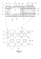
- Fig 5 shows an embodiment of the present invention in which a plurality of cavities is formed in a printed circuit board.
- Fig 5 is a top view on the inventive connection system for electronic components without the upper electrode-group 4 applied so that a bottom electrode 6' can be seen in each cavity 3.
- the plurality of cavities 3 in this preferred embodiment are covered by an insulating layer with appropriately positioned top electrodes 6 as can be seen in the enlarged sectional side view of Fig 5 .
- the walls of insulating layer 2 in the left hand area of the top view of Fig 5 can be reduced to only pillars as in the right hand area of the top view of Fig 5 .
- the plurality of electrodes 6 and 6' form a plurality of capacitors which for example can be used as a track pad or other pointing device for example in a portable computer or smart phone.
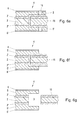
- a cavity in a printed circuit board can be produced starting form a core material comprising an insulating layer 2 and layers of copper 2' and 2".
- the insulating layer 2 preferably has a thickness of between 50 ⁇ m and 1000 ⁇ m and is preferably made of a prepreg material, in particular FR-4.
- the material is cut for example by a laser and subsequently the portion to be removed and separated by the cut 13 is covered with release layer 14 which is well known in the art.
- the release layer 14 also flows into the area of the cut 13 and will prevent firm adhesion of additional layers laminated onto the core material as depicted in Fig 6d .
- the additionally laminated layers are cut for example by a laser and the end of a board with the plug 15 is removed by machining ( Fig 6f ) upon which the plug 15 can be pulled out of the printed circuit board leaving a cavity 3 therein.
- a hole or cavity 3 is provided therein ( Fig 7a and 7b ) and a no-flow-prepreg-material is appropriately cut ( Fig. 7c )) to fix the electrode-groups 4 and 4' to the core material by lamination of the core 2, the no-flow-prepreg-material 17 and the electrode-groups 4 and 4' ( Fig 7d ).
- the process for the production of a plurality of cavities in the inventive printed circuit board involves structuring a cooper-clad-laminate by known methods to obtain an electrode-group 4' ( Fig 8a )) and covering the area of the future cavity with a release layer 14 ( Fig 8b )).
- an insulating layer 2 is laminated onto the electrode-group 4' which is then cut in sections by laser-cutting. The cuts are denoted by reference numerals 18 in Fig 8d ). Accordingly the insulating layer 2 can easily be removed from the electrode-group 4' to yield the cavity 3.
- the cavity 3 can be covered with an electrode-group 4 either by gluing or by laminating with a no-flow-prepreg-material.
Landscapes
- Engineering & Computer Science (AREA)
- Microelectronics & Electronic Packaging (AREA)
- Power Engineering (AREA)
- Physics & Mathematics (AREA)
- General Physics & Mathematics (AREA)
- Manufacturing & Machinery (AREA)
- Acoustics & Sound (AREA)
- Signal Processing (AREA)
- Production Of Multi-Layered Print Wiring Board (AREA)
Priority Applications (2)
| Application Number | Priority Date | Filing Date | Title |
|---|---|---|---|
| EP15166936.3A EP3091821A1 (de) | 2015-05-08 | 2015-05-08 | Leiterplatte |
| US15/147,724 US20160330840A1 (en) | 2015-05-08 | 2016-05-05 | Printed Circuit Board |
Applications Claiming Priority (1)
| Application Number | Priority Date | Filing Date | Title |
|---|---|---|---|
| EP15166936.3A EP3091821A1 (de) | 2015-05-08 | 2015-05-08 | Leiterplatte |
Publications (1)
| Publication Number | Publication Date |
|---|---|
| EP3091821A1 true EP3091821A1 (de) | 2016-11-09 |
Family
ID=53054962
Family Applications (1)
| Application Number | Title | Priority Date | Filing Date |
|---|---|---|---|
| EP15166936.3A Withdrawn EP3091821A1 (de) | 2015-05-08 | 2015-05-08 | Leiterplatte |
Country Status (2)
| Country | Link |
|---|---|
| US (1) | US20160330840A1 (de) |
| EP (1) | EP3091821A1 (de) |
Families Citing this family (5)
| Publication number | Priority date | Publication date | Assignee | Title |
|---|---|---|---|---|
| US10251272B2 (en) * | 2017-06-30 | 2019-04-02 | Intel Corporation | Microelectronic devices designed with ultra-high-k dielectric capacitors integrated with package substrates |
| CN112201652A (zh) * | 2019-07-07 | 2021-01-08 | 深南电路股份有限公司 | 线路板及其制作方法 |
| KR20210078239A (ko) * | 2019-12-18 | 2021-06-28 | 삼성전자주식회사 | 인쇄회로기판 및 이를 구비한 전자 장치 |
| EP4017226A4 (de) * | 2020-07-07 | 2023-07-19 | Shennan Circuits Co., Ltd. | Eingebettete leiterplatte und verfahren zur herstellung einer eingebetteten leiterplatte |
| CN116567926B (zh) * | 2023-07-12 | 2023-11-24 | 信丰迅捷兴电路科技有限公司 | 一种刚挠结合电路板及其制作方法 |
Citations (5)
| Publication number | Priority date | Publication date | Assignee | Title |
|---|---|---|---|---|
| US4555745A (en) * | 1981-11-05 | 1985-11-26 | Preh Elektrofeinmechanische Werke Jakob Preh Nachf. Gmbh & Co. | Thick-film capacitor manufactured by printed-circuit techniques |
| US20120007829A1 (en) * | 2010-07-08 | 2012-01-12 | Freescale Semiconductor, Inc. | Method and system for touch sensor interface fault detection |
| US20120228109A1 (en) * | 2011-03-08 | 2012-09-13 | Ibiden Co., Ltd. | Sensor, keyboard and method for manufacturing sensor |
| US20120274599A1 (en) * | 2011-04-26 | 2012-11-01 | Synaptics Incorporated | Input device with force sensing and haptic response |
| US20130119652A1 (en) * | 2010-07-16 | 2013-05-16 | Novalia Ltd. | Electronic device |
Family Cites Families (6)
| Publication number | Priority date | Publication date | Assignee | Title |
|---|---|---|---|---|
| US5838805A (en) * | 1995-11-06 | 1998-11-17 | Noise Cancellation Technologies, Inc. | Piezoelectric transducers |
| US9028748B2 (en) * | 2006-02-24 | 2015-05-12 | Nanovibronix Inc | System and method for surface acoustic wave treatment of medical devices |
| US7642698B2 (en) * | 2007-03-30 | 2010-01-05 | Intel Corporation | Dual direction rake piezo actuator |
| US8339798B2 (en) * | 2010-07-08 | 2012-12-25 | Apple Inc. | Printed circuit boards with embedded components |
| US9823209B2 (en) * | 2010-10-05 | 2017-11-21 | Anpac Bio-Medical Science Co., Ltd. | Micro-devices for disease detection |
| NL2008459C2 (en) * | 2012-03-09 | 2013-09-10 | Oldelft B V | A method of manufacturing an ultrasound transducer for use in an ultrasound imaging device, and an ultrasound transducer and ultrasound probe manufactured according to the method. |
-
2015
- 2015-05-08 EP EP15166936.3A patent/EP3091821A1/de not_active Withdrawn
-
2016
- 2016-05-05 US US15/147,724 patent/US20160330840A1/en not_active Abandoned
Patent Citations (5)
| Publication number | Priority date | Publication date | Assignee | Title |
|---|---|---|---|---|
| US4555745A (en) * | 1981-11-05 | 1985-11-26 | Preh Elektrofeinmechanische Werke Jakob Preh Nachf. Gmbh & Co. | Thick-film capacitor manufactured by printed-circuit techniques |
| US20120007829A1 (en) * | 2010-07-08 | 2012-01-12 | Freescale Semiconductor, Inc. | Method and system for touch sensor interface fault detection |
| US20130119652A1 (en) * | 2010-07-16 | 2013-05-16 | Novalia Ltd. | Electronic device |
| US20120228109A1 (en) * | 2011-03-08 | 2012-09-13 | Ibiden Co., Ltd. | Sensor, keyboard and method for manufacturing sensor |
| US20120274599A1 (en) * | 2011-04-26 | 2012-11-01 | Synaptics Incorporated | Input device with force sensing and haptic response |
Also Published As
| Publication number | Publication date |
|---|---|
| US20160330840A1 (en) | 2016-11-10 |
Similar Documents
| Publication | Publication Date | Title |
|---|---|---|
| US20160330840A1 (en) | Printed Circuit Board | |
| US9131039B2 (en) | Piezoelectric actuator interface and method | |
| US20120228109A1 (en) | Sensor, keyboard and method for manufacturing sensor | |
| US9899591B2 (en) | Piezoelectric actuator, piezoelectric vibration apparatus, and portable terminal | |
| US20110227866A1 (en) | Sensor apparatus and display apparatus | |
| EP3353112B1 (de) | Verbindungspaneel für elektronische bauelemente | |
| US20130213695A1 (en) | Method of manufacturing flying tail type rigid-flexible printed circuit board and flying tail type rigid-flexible printed circuit board manufactured by the same | |
| WO2015129061A1 (ja) | 圧電アクチュエータおよびこれを備えた圧電振動装置、携帯端末、音響発生器、音響発生装置、電子機器 | |
| JP2005109101A (ja) | 電磁シールド型可撓性回路基板 | |
| KR20150008771A (ko) | 전자소자 내장형 인쇄회로기판 및 그 제조방법 | |
| KR20150125424A (ko) | 강연성 인쇄회로기판 및 강연성 인쇄회로기판의 제조 방법 | |
| JP5730452B1 (ja) | 圧電アクチュエータおよびこれを備えた圧電振動装置、携帯端末、音響発生器、音響発生装置、電子機器 | |
| JP2014229296A (ja) | 電磁誘導タブレット構造及びその製造方法、並びに電磁式手書き入力装置 | |
| CN210629449U (zh) | 压电模组以及电子设备 | |
| JP6363545B2 (ja) | 圧電アクチュエータ、音響発生器、音響発生装置および電子機器 | |
| JP2015126605A (ja) | 圧電アクチュエータおよびこれを備えた圧電振動装置、携帯端末、音響発生器、電子機器 | |
| US10165685B2 (en) | Printed circuit board | |
| JP2018125605A (ja) | 圧電アクチュエータ、圧電振動装置および電子機器 | |
| JP2016111359A (ja) | 電子部品内蔵印刷回路基板及びその製造方法 | |
| JP4785473B2 (ja) | 多層プリント配線板、多層プリント配線板の製造方法、及び電子装置 | |
| WO2013157355A1 (ja) | 圧電振動素子ならびにそれを用いた圧電振動装置および携帯端末 | |
| CN108925028A (zh) | 一种柔性电路板、阵列基板、显示面板及显示装置 | |
| JPWO2008020478A1 (ja) | 機構部品内蔵基板及びその製造方法 | |
| US20160179202A1 (en) | Touch device and electronic equipment using the same | |
| KR20120006916A (ko) | 인쇄회로 스티커 및 단층 금속 터치패드 제조 방법 |
Legal Events
| Date | Code | Title | Description |
|---|---|---|---|
| PUAI | Public reference made under article 153(3) epc to a published international application that has entered the european phase |
Free format text: ORIGINAL CODE: 0009012 |
|
| AK | Designated contracting states |
Kind code of ref document: A1 Designated state(s): AL AT BE BG CH CY CZ DE DK EE ES FI FR GB GR HR HU IE IS IT LI LT LU LV MC MK MT NL NO PL PT RO RS SE SI SK SM TR |
|
| AX | Request for extension of the european patent |
Extension state: BA ME |
|
| 17P | Request for examination filed |
Effective date: 20170508 |
|
| RBV | Designated contracting states (corrected) |
Designated state(s): AL AT BE BG CH CY CZ DE DK EE ES FI FR GB GR HR HU IE IS IT LI LT LU LV MC MK MT NL NO PL PT RO RS SE SI SK SM TR |
|
| 17Q | First examination report despatched |
Effective date: 20190517 |
|
| STAA | Information on the status of an ep patent application or granted ep patent |
Free format text: STATUS: THE APPLICATION IS DEEMED TO BE WITHDRAWN |
|
| 18D | Application deemed to be withdrawn |
Effective date: 20190928 |